Wireless DAQ using LabVIEW
|
|
|
- Amber Goodwin
- 6 years ago
- Views:
Transcription

1 Indiana University Purdue University Fort Wayne Opus: Research & Creativity at IPFW Engineering Senior Design Projects School of Engineering, Technology and Computer Science Design Projects Wireless DAQ using LabVIEW Anish Mathew Todd Hauter Berel McClellan Geoffry Mungai Follow this and additional works at: Part of the Engineering Commons Opus Citation Anish Mathew, Todd Hauter, Berel McClellan, and Geoffry Mungai (2010). Wireless DAQ using LabVIEW. This Senior Design Project is brought to you for free and open access by the School of Engineering, Technology and Computer Science Design Projects at Opus: Research & Creativity at IPFW. It has been accepted for inclusion in Engineering Senior Design Projects by an authorized administrator of Opus: Research & Creativity at IPFW. For more information, please contact
2 Indiana University Purdue University Fort Wayne Department of Engineering ECE 406 Capstone Senior Design Project Project Title: Team Members: Faculty Advisor: Wireless DAQ using LabVIEW Anish Mathew, Todd Hauter, Berel McClellan, Geoffry Mungai Dr. Abdullah Eroglu Date: December 11,
3 Table of Contents Acknowledgement 3 Abstract/ Summary 4 Section I: Conceptual Design 5 Section II: Building Process 27 Section III: Testing 38 Evaluation and Recommendation 43 Conclusion 44 Appendix A: 45 2
4 Acknowledgement We would like to extend our gratitude to our faculty advisor Dr. Eroglu for his continuing support and dedicated guidance in the development and formulation of this project. We would also like to thank Bob from the IPFW technology department for helping us get the parts soldered on and Prof. Dewitt for his feedback and recommendations throughout the semester. Without their contribution, this project would have never been fully realized. And finally, a thank the entire Department of Engineering faculty at IPFW for giving us the opportunity to earn and apply the prerequisite knowledge and education that was put to work during this project. 3
5 Abstract This paper is written as a continuation of the spring 2010 semester of work on the wireless data acquisition system using LabVIEW software. The project is the result of work done by senior design students in the Indiana University Purdue University School of Engineering, Technology and Computer Science. This document is a written record of the process of building a final prototype based on the problems statement and chosen conceptual design on the previous semester. The proposal of the previous semester was to build a wireless data acquisition system and then process the conditioned signal through labview software. This report reviews the selected conceptual design of the previous semester, a brief description of the building process and any changes made to the conceptual design, testing results, the groups evaluations and recommendations, and a final conclusion to this project. Information will be provided for all of our processes, our reasoning, and final conclusions. All schematics, research, and calculations are provided for reference and understanding. 4
6 Section I: Conceptual Design 5
7 Concepts: After researching these options, it was decided to narrow down our design possibilities by looking at which designs might and might not be possible to implement. We ended up with three remaining design concepts which included a switch circuit using the YS C30H transceiver pair, Encoded signal circuit using a microcontroller and YS C30H transceiver pair and a multichannel transceiver/receiver pair made by RF Solutions Concept 1: Switch Circuit using the YS C30H transceiver pair Description: The fist concept is based around the idea of using a switch to select which measurement signal will be sent through the conditioning circuit to the transmitter. This circuit creates minimal interaction between the different measurement circuits and allows for a segmented circuit design. In this design we have a separate circuit for each of our measurement devices. The output of the measurement circuits will be fed into a switch which will be used to select the user's preferred signal. The preferred signal will then be sent to an A/D converter where it will be converted into a digital signal and then be sent to a universal asynchronous receiver/transmitter (UART) to prepare the data to be converted into a RS 232 signal by being sent into an RS 232 line driver. At this point the signal will be sent into the YS C30H transceiver and be transmitted wirelessly to the YS C30H being used as a receiver. During the wireless transmission the signal will be sent at one of the three frequencies supported by the YS C30H which are 433 MHz, 868 MHz and 945 MHz. From the receiver the transmitted signal will be sent to RS 232 R/D line driver and then be sent through another UART to convert the signal back into the digital signal that was outputted from the A/D converter. The signal will then be sent through a D/A converter and then be fed into the SC 2345 DAQ and be sent to a computer terminal using LabView. Each stage of this system can be described by a different section of hardware. The discrete hardware stages are displayed in Figure 1. In this concept a YS C30H transceiver pair is used to wirelessly transmit the signal in the design. This transceiver pair was chosen because it meets the distance requirements set for the project, leaves money in the budget for the conditioning circuits and the transceivers are made to work in combination with each other. The first concept also uses discrete parts to construct our conditioning circuits. Due to the use of the YS C30H we are also using the RS 232 signal protocol. The main feature of this circuit is it removes the need to encode the different measurement circuits into on signal by using a switch that a user can use to select the measurement device which they wish to use. 6
8 Measurement Devices and Corresponding Circuits Pre-Transmission Signal Conditioning Circuit Measurement Device Selection Switch Signal Conditioning / Control Signals A/D Converter UART RS-485 D/R Line Driver YS-C30H Wireless Transceiver ACK Signal Wirelessly Transmitted Signal YS-C30H Wireless Transceiver Post-Receiver Signal Conditioning Circuit RS-485 R/D Line Driver UART D/A Converter Signal Conditioning /Control Signals LabVIEW User Interface on Computer SC-2345 DAQ Figure 1: Concept 1 Block Diagram 7
9 Concept 2: Circuit using the RF Solutions Description: This concept is created around the idea of sending multiple data signal simultaneously. A block diagram of this design is shown in Figure 2. Each of the measuring instruments will use a unique circuit to develop a signal in the range that is usable by the analog to digital converter where it will be converted into a digital signal and then sent to RF solution wireless transmitter. The RF solution transceiver is used to transmit the data up to 10km. This is a high end transmitter and receiver pair which is very expensive. The cost of this instrument exceeds our budget. The signal received is then fed into a post receiver signal conditioning circuit. SC 2345 DAQ receives the signal and then sent to LabVIEW user interface on computer. Measurement Devices and Corresponding Circuits Pre-Transmission Signal Conditioning Circuit Signal Conditioning A/D Converter RF Solutions Wireless Transmitter RF Solutions Wireless Receiver Post-Receiver Signal Conditioning Circuit D/A Converter Signal Conditioning LabVIEW User Interface on Computer SC-2345 DAQ Figure 2: Concept 2 Block Diagram 8
10 Concept 3: Multiplexing Circuit using the YS C30H transmitter and YS 20UA receiver Description: This concept is created around the idea of sending multiple data signals across one RF channel. A block diagram of this design is shown in Figure 3. Each of the measuring instruments will use a unique circuit to develop a signal in the range that is usable by the Analog to Digital Converter (ADC). The measuring circuits are connected either directly to a multi channel ADC, or to a single channel ADC via a multiplexer. A microcontroller will be used to select which signal to convert and to command the DAC to begin the conversion process. The microcontroller will either cycle through each input channel, or for a small additional cost, will cycle through only the input channels selected by means of DIP switches. Once the conversion is complete the digitized value is transferred to the microcontrollers memory. The address of the multiplexer used to select the signal is appended to the signals value. This combined data packet is then loaded into a UART, converting the data packet into a bit stream. The next stage is an RS232 line driver which converts the TTL bit stream into higher voltage RS232 bit stream in order to communicate with the YS 30H transmitter. The YS 30H transceiver is used to transmit the signal up to 10 Km, if both the transmitter and receiver are in the open with direct line of sight. The range of the signal is reduced by the amount of obstructions between the transmitter and receiver. Since it is not necessary to have two way communication between the transmitter and receiver pair, a lower power YS 20UA transceiver is used to capture the bit stream. The bit stream is loaded into the memory of the second microcontroller via a UART connected to an RS232 line receiver. This microcontroller then removes the appended address from the digitized signal. The address is used by the microcontroller to select which output channel of the multiplexer to use. An Analog to Digital Converter (ADC) is used to change the digital signal back into analog. Each output channel of the multiplexer is connected to a different input channel of the SC 2345 DAQ and from there into the LabView software. A program written for LabView will identify each channel as a different measured parameter, and using mathematical models of the measuring devices, convert the signals into the actual value of the measured parameter. 9
11 Measurement Devices and Corresponding Circuits Pre-Transmission Signal Conditioning Circuit Measurement Device Selection Switch Signal Conditioning A/D Converter MCU Memory MCU Control RS-485 D/R Line Driver UART YS-C20UA Wireless Transceiver Wirelessly Transmitted Signal YS-C30H Wireless Transceiver Post-Receiver Signal Conditioning Circuit MCU Memory D/A Converter MCU Control Multiplexer RS-485 R/D Line Driver UART LabVIEW User Interface on Computer SC-2345 DAQ Figure 3: Concept 3 Block Diagram Concept 4: YS C30H Pair Using Multiplexer 10
12 Measurement Devices and Corresponding Circuits Pre-Transmission Signal Conditioning Circuit Measurement Device Selection Switch Signal Conditioning A/D Converter MCU Memory MCU Control RS-485 D/R Line Driver UART YS-C30H Wireless Transceiver Wirelessly Transmitted Signal YS-C30H Wireless Transceiver ACK Signal Post-Receiver Signal Conditioning Circuit MCU Memory D/A Converter MCU Control Multiplexer RS-485 R/D Line Driver UART LabVIEW User Interface on Computer SC-2345 DAQ Figure 4: Concept 4 Block Diagram 11
13 Input measuring circuits There are three different types of measurements being made; displacement (strain), temperature, and acceleration. Each of these types of measurements requires a different circuit to convert the measured parameter into an electrical signal at a level safe to apply to the ADC. These circuits will use a common power supply of 15 VDC. Strain: A Wheatstone bridge will be used to measure the minute change in resistance of the strain gauge. This circuit is represented in Figure 5. Figure 5: Strain Measuring Circuit 12
14 Temperature: The user will have a choice of using an RTD or a thermistor to measure temperature. Each of these devices will use a voltage divider in order to develop the input signal for the ADC as shown in Figure 6. However since these devices do not have the same resistance values, the voltage dividers are necessarily different. A double pole double throw switch is used to select which signal is sent to the multiplexer and also to tell the encoding device which signal is present so the correct mathematical model can be used when decoding the signal. V1 15 V R1 216Ω R2 6400Ω J1 to Multiplexer RTD T1 HEL-700-U0B Key = T THM U1 thermistor Key = Space RTD - THM - Figure 6: Temperature Measuring Circuit 13
15 Final Concept Design: 14
16 The final concept is created around the idea of sending multiple data signals across one RF channel. A block diagram of this design is shown in Figure 4. Each of the measuring devices will use a unique circuit to develop a signal in the range that is usable by the Analog to Digital Converter (ADC). The measuring circuits are connected either directly to a multi channel ADC, or to a single channel ADC via a multiplexer. A microcontroller will be used to select which signal to convert and to command the DAC to begin the conversion process. The MCU will be used to poll and send measurement signals that are chosen through a LabVIEW program. The selected signal is then sent through an internal UART of a MCU and then sent in to a RS 485 Line Driver so that it is able to be transmitted through the YS 30H. The YS 30H transceiver is used to transmit the signal up to 10 Km, if both the transmitter and receiver are in the open, with direct line of sight. The range of the signal is reduced by the amount of obstructions between the transmitter and receiver. A MCU on the Reception side of the circuit is used in conjunction with a digital to analog converter to convert the signals in to a analog voltage signal that is sent into the SC 2345 DAQ and the LabVIEW program. The MCU also creates an acknowledgement/select signal that is sent through the MCU UART and a RS 485 Line Driver and is sent back through the reception YS C30H transceiver back to the transmission circuit. The LabVIEW program then uses a voltage to measurement and signal transmitted to create a signal to determine which measurement device the signal comes from. The LabVIEW program then uses specific conversion for the specific measurement device. The LabVIEW program then also displays the converted values to the user. The LabVIEW program also allows the user to create a signal that allows the user to select which measurement devices will be polled. 15
17 Measurement Devices and Corresponding Circuits Pre-Transmission Signal Conditioning Circuit MUX A/D Converter MCU Memory MCU Control RS-485 Line Driver MCU UART YS-C30H Wireless Transceiver Wirelessly Transmitted Signal YS-C30H Wireless Transceiver ACK Signal Post-Receiver Signal Conditioning Circuit RS-485 Line Driver Acknowledge/Selection Signal MCU Control D/A Converter MCU Memory RS-485 Line Driver MCU UART LabVIEW User Interface on Computer Select Signal SC-2345 DAQ Selection Signal Figure 7: Overall Final Design Flowchart 16
18 Transmission MCU The transmission circuit is controlled by a C8051F340 MCU. There are two input signals that are sent into the MCU. There is a measurement signal and an acknowledgement and select signal. The digital measurement signal comes from one of the five measurement devices that had been polled by the MCU and the analog to digital converter. The acknowledgement and select signal comes from a transmission from the receiving transceiver. A flow chart that is illustrating the transmission portion is given in Fig. 8. Transmission MCU Output Signals Sampling Code Signal Splitting UART Input Signals 12-bit Digital Measurement Signal MCU UART 12-bit Measurement Signal 3-bit Mux Select Signal To Measurement Multiplexer Sampling Code 10-bit Acknowledge/Select Signal Split Acknowledge Signal and Select Signal 15-bit Encoded Measurement Signal 5-bit Select Signal Measurement Signal to RS Line Driver Acknowledge Signals MCU Clock To Acknowledgement Circuit Figure 8: Transmission MCU 17
19 Receiver MCU The receiver circuit is controlled by a C8051F340 MCU. There are two input signals that are sent to the receiver MCU. There is a measurement signal from the transmitter and a select signal. The measurement signal from the transmitter is composed of a measurement signal from one of the measurement devices and identification signal from measurement device. The select signal is a user defined signal that is defined in the LabVIEW program. A flow chart for the transmission MCU can be seen in Figure 9. Receiver MCU Output Signals Sampling Code D/A Converter MCU UART Signal Splitting Input Signals MCU Clock 15-bit Transmitted Signal Split 3-bit Label and 12-bit Measurement Signal 12-bit Measurement Signal MCU UART 12-bit Measurement Signal D/A Converter SC-2345 DAQ using 3 digtal input ports Check if Signal is Selected Combine Acknowledge and Select Signal UART 3-bit Label 5-bit Select Signal Check to see if Transmitted Signal is one of the Selected Signals 5-bit Acknowledg e Signal Combine Acknowledge and Select Signal 10-bit Select/ Acknowledge Signal MCU UART 10-bit Select Acknowledge Signal To RS-485 Line Driver Figure 9: Receiver MCU Flowchart 18
20 Yes Yes Yes LabVIEW Flowchart The LabVIEW program receives two input signals; measurement signal and identification signal. The measurement signal comes into the SC 2345 DAQ using of the input channel. The program then determines the measurement device that the signal is coming from. The signal is then sent to a corresponding Voltage to measurement unit conversion program. These conversions are based on the calculations and equations in Appendix A. After the unit conversion, the converted measurements are displayed to the user. A flow chart for the transmission MCU can be seen in Figure 10. LabVIEW Flowchart Signal User Display Signal Determination Calculations 5 V Input Input Signals 3-bit Label Using digital input Ports If Label=0 Yes Voltage to strain unit conversion Strain Gauge display No If Label =1 Voltage to Hz unit conversion LDS display No If Label =2 Voltage to Hz unit conversion Accelerometer display No If Label =3 Voltage to Degrees C and K unit conversion Thermister display No Else Yes Voltage to Degrees C and K unit conversion RTD display User Defined Signals Output Signals 5-bit User defined selection signal 5-bit output using digital output ports of SC-2345 Figure 10: LabVIEW Flowchart 19
21 Input interface circuit: Purpose: The primary purpose of the input interfacing circuit is to sample the desired signals, convert them to a digital format, and forward the digitized signal to the transmitter. A secondary function is to provide a visual acknowledgement of which signals have been received at the output circuit. Overview: The input circuit microcontroller receives a signal from the microcontroller at the output interfacing circuit. This signal is composed of two parts. The first part of the signal is used to determine which channels are to be sampled. The last part is used to generate the visual acknowledgement. The microcontroller will rotate sampling each of the desired channels. The first step that the microcontroller performs is to command the DAC to generate a reference signal. The sensitivity of the ADC is adjusted by varying its reference. The second step the microcontroller performs is to inform the ADC which channel to sample. The microcontroller then gives the ADC the command to begin conversion. While the conversion is in progress, the microcontroller will determine which signal has been received by the output interface circuit. Then it informs the LED driver which acknowledge LED to energize. The next step in the process is to accept the digitized signal from the ADC. The microcontroller then appends addition to this signal. The signal is then sent to a RS485 driver/receiver via an internal UART. The RS485 D/R sends the data to the output interface via a wireless transceiver. Components: Silicon Labs C8051F340 microcontroller: The microcontroller is used to control the order in which all of the operations are performed. The core of the microcontroller uses pipeline architecture and executes 70% of all instructions in one or two system clocks. The controller can perform 48million instructions per second, and has 4352 bytes of RAM. The controller has 40 I/O ports and supports SPI, SMBus, and UART serial ports. EXAR RS 485 Receiver/Driver: The RS485 R/D is used to interface between the microcontroller and the wireless transceiver. This device has a maximum data rate of 20 Mbps in full duplex mode. NXP Semiconductors PCA9551 LED driver: The LED driver communicates using I 2 C bus communication. This is compatible with the SMBus format that the microcontroller uses. The driver contains 8 open drain outputs which can directly drive LED s to 25mA. 20
22 Linear Technology LTC2308 Analog to Digital Converter: The ADC is used to sample an analog signal and convert the sample to a digital value. This 12 bit ADC has a maximum sample rate of 250ksps. The ADC also contains an 8 channel internal multiplexer which can be used as 8 single ended inputs, 4 differential inputs, or any combination of the two types. In addition the signal may be either unipolar or bipolar. The ADC communicates with the microcontroller via Serial Peripheral Interface (SPI). The ADC may use either its internal reference of 4.096V or an external reference. Linear Technology LTC1257 Digital to Analog Converter: In this circuit the DAC is used to generate the desired reference signal for the ADC. This device also communicates with the microcontroller via SPI. A 12 bit DAC is somewhat of an overkill for this application, but the component was chosen since it is already used in the output interface circuit. Figure 11: Input interface Circuit 21
23 Output interface circuit: Purpose: The function of the output interface circuit is to convert the digital signal received from the input interface into an analog output which is directed into a DAQ signal conditioning module. This circuit also informs the input interface which channels need to be sampled and the last signal it received. Overview: The microcontroller receives an input from the DAQ. These bits represent which input channels need to be sampled. The microcontroller appends addition to the acknowledgement of the last sample received and sends it to the wireless transceiver via an internal UART and an RS485 D/R. Upon reception of the signal from the input interface, the microcontroller will separate the specified address from the data signal. The data signal is sent to the DAC which recreates the sampled input and sends it to the DAQ signal conditioning module. The added address is sent directly to the DAQ so that the Labview Software will know which signal it has received. Components: Silicon Labs C8051F340 microcontroller: The microcontroller is used to control the order in which all of the operations are performed. The core of the microcontroller uses pipeline architecture and executes 70% of all instructions in one or two system clocks. The controller can perform 48million instructions per second, and has 4352 bytes of RAM. The controller has 40 I/O ports and supports SPI, SMBus, and UART serial ports. EXAR RS 485 Receiver/Driver: The RS485 R/D is used to interface between the microcontroller and the wireless transceiver. This device has a maximum data rate of 20 Mbps in full duplex mode. Linear Technology LTC1257 Digital to Analog Converter: In this circuit the 12 bit DAC is used to recreate the sampled input signal. This device communicates with the microcontroller via SPI. 22
24 Figure 12: Output interface Circuit 23
25 Changes from Original Design: 24
26 Selected radio YS C30H to ConnexLink 4790 The radio change was necessary since the YS C30H does not fall into the ISM frequency band in the United States. This also required a change in communication between the MCUs and radios from RS 485 to RS 232. The chart below shows how to select an operating frequency in the United States. Specification of ConnexLink 4790 Max RS 232 transmission rate: 115.2Kbps Wireless transmission rate: 76.8 Kbps 900 MHz Frequency Hopping Spread Spectrum modulation Range: up to 20 miles line of sight Range indoors: 1500 m 25
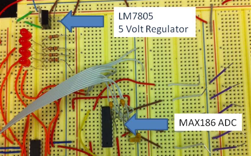
27 ADC LTC2308 to MAX186 Original ADC: LTC2308 QFN 24 package with center ground pad. Max sample rate: 500 khz New ADC: MAX pin DIP Max sample rate: 133 khz 12 bit SAR. Both single and differential channel inputs. Internal 4.096V reference 5 volt regulation circuit Zener Diode network to LM7805 Zener Diode network Max VDD for ADC limited to 5.25V Simulation provided a max voltage of 5.1V Implementation resulted in over 5.3V LM7805 Voltage stable at 4.95 V in both simulation and implementation. 26
28 Building Process: 27

29 ADC/DAC Simulation: Calculation: 12 bit ADC encodes the analog input in 4096 levels 2 12 = 4096 Dout = decimal value of the binary output Vin= analog input Vref= reference voltage of the ADC = 5V N= bits=12 D out Vin V = 2 ref n 28

30 Transmitter Multisim Layout 29
31 Transmitter Interface Circuit: 30

32 PCB Layout in Ultiboard Input Board View 31

33 Output Circuit Board 32


34 Receiver Interface Circuit: Output Board View 33


35 3D Output MCU software development using silicon laboratories C8051 F340 TB Following is the combined code flow chart: Transmitter MCU flowchart: 34
36 35
37 Receiver Flow Chart: 36
38 LabVIEW LabVIEW is a graphical programming environment used by millions of engineers and scientists to develop sophisticated measurement, test, and control systems using intuitive graphical icons and wires that resemble a flowchart. It offers unrivaled integration with thousands of hardware devices and provides hundreds of built in libraries for advanced analysis and data visualization all for creating virtual instrumentation. The LabVIEW platform is scalable across multiple targets and OSs, and, since its introduction in 1986, it has become an industry leader. The issues faced when using LabVIEW are the following: Compatibility Issues Legacy vs. DAQmx NI website is not updated Solutions used to solve the problems faced in the project are the following: Able to find solutions after lot of research. Help from the Indiana LabVIEW Users Group ( Prof. Edward Dewitt Technology department) 37
39 Testing 38


40 Analog to Digital Converter communication Digital to Analog Converter communication 39


41 LabVIEW Files Screen shots of the labview files for the following measurements: RTD Block Diagram: Strain 40

42 Block Diagram: Thermistor: Block Diagram: 41


43 Voltage: Block Diagram: 42
44 Recommendations A recommendation to any future Senior Design group is to verify that they have access to the equipment necessary to implement their design. In our case, we had chosen an ADC with a QFN 24 footprint with an additional ground pad in the center of the bottom. The leads on this package are all recessed under the chip. After a couple of attempts the Technology Department was able to cut a board for us. However, because of the chip s architecture, they were unable to solder good connections to all of the pins. We were forced to select a new ADC with a different footprint, resulting in at least a week and a half delay of implementing the design. If reworking this project, we recommend adding external memory to the MCU s. Several times during the software development we were forced to recode the software due to running out of available memory. Also, better error detection and correction algorithms could be implemented. In addition to this the radios could be placed in the API mode, which would allow several bytes of data to be bundled into one packet. Currently the radios are in a transparent mode, each byte is transmitted as it is received. Another recommendation would be to find a different software development platform. The platform included with the C0851F340 development board left a lot to be desired. It is essentially an evaluation product. We noticed that as the project code became longer, the less specific the error codes became. The compiler also did not have any predefined functions like in Embedded RTOS, which would have helped simplify the coding. Finally, we realize that you have to work with the equipment specified by your customer. However, eventually one must bite the bullet and upgrade obsolete equipment. The software for the DAQpad equipment the school has was last supported by Windows XP. National Laboratories has new software for current operating systems, but this software does not function with the Legacy DAQpad equipment. We recommend checking the technical support available for any legacy equipment you must work with. If none is available, explore the option of a possible upgrade. 43
45 Conclusion: We have demonstrated the ability to capture, send data wirelessly and reconstruct any analog signal. We have also proved that the radios have a range of at least 1.5 mile. This range can be extended by using different antennas. The wirelessly sent signals can be processed through LabVIEW. Our design is scalable for applications in medical field, construction industry and household applications. 44
46 Appendix A: Compliance ISM band: 6020E User manual: Ultiboard User Manual: SC 2345 LM 7805 MAX186 MAX188 LabVIEW getting started C8051 Radio User manual: C:\Users\Anish\Desktop\Senior Design 2\compliance ism band.pdf C:\Users\Anish\Desktop\Senior Design 2\6020Eusermanual.pdf C:\Users\Anish\Desktop\Senior Design 2\Ultiboard User Manual.pdf C:\Users\Anish\Desktop\Senior Design 2\sc2345.pdf C:\Users\Anish\Desktop\Senior Design 2\LM7805.pdf C:\Users\Anish\Desktop\Senior Design 2\MAX186 MAX188.pdf C:\Users\Anish\Desktop\Senior Design 2\LV_Getting_Started.pdf C:\Users\Anish\Desktop\Senior Design 2\C8051F34x.pdf C:\Users\Anish\Desktop\Senior Design 2\4790User Manualv1.8.pdf 45
TMS320F241 DSP Boards for Power-electronics Applications
 TMS320F241 DSP Boards for Power-electronics Applications Kittiphan Techakittiroj, Narong Aphiratsakun, Wuttikorn Threevithayanon and Soemoe Nyun Faculty of Engineering, Assumption University Bangkok, Thailand
2.0 Discussion: 2.1 Approach:
 2.0 Discussion: 2.1 Approach: The design for a Power Monitor and Data Logging System is comprised of two major components: the Power Meter and the Data Logger. The Power Meter is the package that plugs
Preliminary GHz Transceiver-µController-Module. Applications PRODUCT SPECIFICATION FEATURES MICROCONTROLLER MHz
 PRODUCT SPECIFICATION 2.4 2.5 GHz e Applications 6 : 2 " 2! 2 2 + 2 7 + + Alarm and Security Systems Video Automotive Home Automation Keyless entry Wireless Handsfree Remote Control Surveillance Wireless
ADVANCED EMBEDDED MONITORING SYSTEM FOR ELECTROMAGNETIC RADIATION
 98 Chapter-5 ADVANCED EMBEDDED MONITORING SYSTEM FOR ELECTROMAGNETIC RADIATION 99 CHAPTER-5 Chapter 5: ADVANCED EMBEDDED MONITORING SYSTEM FOR ELECTROMAGNETIC RADIATION S.No Name of the Sub-Title Page
Lab 12 Laboratory 12 Data Acquisition Required Special Equipment: 12.1 Objectives 12.2 Introduction 12.3 A/D basics
 Laboratory 12 Data Acquisition Required Special Equipment: Computer with LabView Software National Instruments USB 6009 Data Acquisition Card 12.1 Objectives This lab demonstrates the basic principals
Development of a MATLAB Data Acquisition and Control Toolbox for BASIC Stamp Microcontrollers
 Chapter 4 Development of a MATLAB Data Acquisition and Control Toolbox for BASIC Stamp Microcontrollers 4.1. Introduction Data acquisition and control boards, also known as DAC boards, are used in virtually
Environmental ADC Interface P Team Members
 Environmental ADC Interface P14346 Team Members Caleb Stephens- Electrical Engineer Kevin Oswald- Electrical Engineer Ory Maimon- Electrical Engineer Edward Wlodarczyk- Electrical Engineer Marissa Fox-
In this lecture, we will look at how different electronic modules communicate with each other. We will consider the following topics:
 In this lecture, we will look at how different electronic modules communicate with each other. We will consider the following topics: Links between Digital and Analogue Serial vs Parallel links Flow control
Training Schedule. Robotic System Design using Arduino Platform
 Training Schedule Robotic System Design using Arduino Platform Session - 1 Embedded System Design Basics : Scope : To introduce Embedded Systems hardware design fundamentals to students. Processor Selection
A Solar-Powered Wireless Data Acquisition Network
 A Solar-Powered Wireless Data Acquisition Network E90: Senior Design Project Proposal Authors: Brian Park Simeon Realov Advisor: Prof. Erik Cheever Abstract We are proposing to design and implement a solar-powered
Using Z8 Encore! XP MCU for RMS Calculation
 Application te Using Z8 Encore! XP MCU for RMS Calculation Abstract This application note discusses an algorithm for computing the Root Mean Square (RMS) value of a sinusoidal AC input signal using the
Project Final Report: Directional Remote Control
 Project Final Report: by Luca Zappaterra xxxx@gwu.edu CS 297 Embedded Systems The George Washington University April 25, 2010 Project Abstract In the project, a prototype of TV remote control which reacts
DNT24MCA DNT24MPA. Low Cost 2.4 GHz FHSS Transceiver Modules with I/O. DNT24MCA/MPA Absolute Maximum Ratings. DNT24MCA/MPA Electrical Characteristics
 - 2.4 GHz Frequency Hopping Spread Spectrum Transceivers - Direct Peer-to-peer Low Latency Communication - Transmitter RF Power Configurable - 10 or 63 mw - Built-in Chip Antenna - 250 kbps RF Data Rate
HC-12 Wireless Serial Port Communication Module
 HC-12 Wireless Serial Port Communication Module User Manual version 2.3C (updated from v1.1 English and v2.3 Chinese) Product Applications Wireless sensor Community building security Robot wireless control
DISCONTINUED. Modulation Type Number of RF Channels 15
 RFM Products are now Murata products. 2.4 GHz Spread Spectrum Transceiver Module Small Size, Light Weight, Built-In Antenna Sleep Current less than 3 µa FCC, Canadian IC and ETSI Certified for Unlicensed
I hope you have completed Part 2 of the Experiment and is ready for Part 3.
 I hope you have completed Part 2 of the Experiment and is ready for Part 3. In part 3, you are going to use the FPGA to interface with the external world through a DAC and a ADC on the add-on card. You
DNT90MCA DNT90MPA. Low Cost 900 MHz FHSS Transceiver Modules with I/O
 - 900 MHz Frequency Hopping Spread Spectrum Transceivers - Direct Peer-to-peer Low Latency Communication - Transmitter Power Configurable to 40 or 158 mw - Built-in 0 dbi Chip Antenna - 100 kbps RF Data
Wireless Music Dock - WMD Portable Music System with Audio Effect Applications
 Wireless Music Dock - WMD Portable Music System with Audio Effect Applications Preliminary Design Report EEL 4924 Electrical Engineering Design (Senior Design) 26 January 2011 Members: Jeffrey Post and
DNT2400. Low Cost 2.4 GHz FHSS Transceiver Module with I/O
 2.4 GHz Frequency Hopping Spread Spectrum Transceiver Point-to-point, Point-to-multipoint, Peer-to-peer and Tree-routing Networks Transmitter Power Configurable from 1 to 63 mw RF Data Rate Configurable
RF4463F30 High Power wireless transceiver module
 RF4463F30 High Power wireless transceiver module 1. Description RF4463F30 adopts Silicon Lab Si4463 RF chip, which is a highly integrated wireless ISM band transceiver chip. Extremely high receive sensitivity
VT-CC M Wireless Module. User Guide
 Wireless Module User Guide V-CHIP MICROSYSTEMS Co. Ltd Address: Room 612-613, Science and Technology Service Center Building, NO.1, Qilin Road, Nanshan District, Shenzhen, Guangdong TEL:0755-88844812 FAX:0755-22643680
EECE494: Computer Bus and SoC Interfacing. Serial Communication: RS-232. Dr. Charles Kim Electrical and Computer Engineering Howard University
 EECE494: Computer Bus and SoC Interfacing Serial Communication: RS-232 Dr. Charles Kim Electrical and Computer Engineering Howard University Spring 2014 1 Many types of wires/pins in the communication
SNIOT702 Specification. Version number:v 1.0.1
 Version number:v 1.0.1 Catelog 1 Product introduction... 1 1.1 Product introduction... 1 1.2 Product application... 1 1.3 Main characteristics... 2 1.4 Product advantage... 3 2 Technical specifications...
PC-based controller for Mechatronics System
 Course Code: MDP 454, Course Name:, Second Semester 2014 PC-based controller for Mechatronics System Mechanical System PC Controller Controller in the Mechatronics System Configuration Actuators Power
SynthNV - Signal Generator / Power Detector Combo
 SynthNV - Signal Generator / Power Detector Combo The Windfreak SynthNV is a 34.4MHz to 4.4GHz software tunable RF signal generator controlled and powered by a PC running Windows XP, Windows 7, or Android
CDR-915 Data Radio Module INTEGRATOR S GUIDE
 CDR-915 Data Radio Module Coyote DataCom, Inc. 3941 Park Drive, Suite 20-266, El Dorado Hills, CA 95762 Tel. 916-933-9981 Fax 916-913-0951 www.coyotedatacom.com TABLE OF CONTENTS General Information and
CL4790 HARDWARE INTEGRATION GUIDE VERSION 3.0. Americas: Europe: Hong Kong:
 CL4790 HARDWARE INTEGRATION GUIDE VERSION 3.0 Americas: +1-800-492-2320 FCC Notice WARNING: This device complies with Part 15 of the FCC Rules. Operation is subject to the following two conditions: (1)
Wireless Sensor Network for Intra-Venous Fluid Level Indicator Application
 Wireless Sensor Network for Intra-Venous Fluid Level Indicator Application Abstract Wireless sensor networks use small, low-cost embedded devices for a wide range of applications such as industrial data
GENESIS TECH PROJECT
 PROJECT! Director Albert Byun! Assistant Director Amar Bhayani! Consultant Engineer Abdul Kalash! Microcontroller Engineer Hirenkumar Patel! Sensor Engineer Shih-Yang Yen Introduction! Problem Statement!
School of Engineering Science Burnaby, BC V5A 1S6. November 2, 2009
 November 2, 2009 Dr. John Bird School of Engineering Science Simon Fraser University Burnaby, British Columbia V5A 1S6 Dear: Dr. Bird and Mr. Whitmore, The attached document presents the design specification
AC : THE UBIQUITOUS MICROCONTROLLER IN MECHANICAL ENGINEERING: MEASUREMENT SYSTEMS
 AC 8-1513: THE UBIQUITOUS MICROCONTROLLER IN MECHANICAL ENGINEERING: MEASUREMENT SYSTEMS Michael Holden, California Maritime Academy Michael Holden teaches in the department of Mechanical Engineering at
RF4432 wireless transceiver module
 1. Description www.nicerf.com RF4432 RF4432 wireless transceiver module RF4432 adopts Silicon Lab Si4432 RF chip, which is a highly integrated wireless ISM band transceiver. The features of high sensitivity
Faculty of Information Engineering & Technology. The Communications Department. Course: Advanced Communication Lab [COMM 1005] Lab 6.
![Faculty of Information Engineering & Technology. The Communications Department. Course: Advanced Communication Lab [COMM 1005] Lab 6.](/thumbs/90/102233011.jpg "Faculty of Information Engineering & Technology. The Communications Department. Course: Advanced Communication Lab [COMM 1005] Lab 6.") Faculty of Information Engineering & Technology The Communications Department Course: Advanced Communication Lab [COMM 1005] Lab 6.0 NI USRP 1 TABLE OF CONTENTS 2 Summary... 2 3 Background:... 3 Software
Faculty of Information Engineering & Technology The Communications Department Course: Advanced Communication Lab [COMM 1005] Lab 6.0 NI USRP 1 TABLE OF CONTENTS 2 Summary... 2 3 Background:... 3 Software
Wireless Master-Slave Embedded Controller for a Teleoperated Anthropomorphic Robotic Arm with Gripping Force Sensing
 Wireless Master-Slave Embedded Controller for a Teleoperated Anthropomorphic Robotic Arm with Gripping Force Sensing Presented by: Benjamin B. Rhoades ECGR 6185 Adv. Embedded Systems January 16 th 2013
Operational Description
 Operational Description Wallterminal WT2000 ISO Tagit The Wallterminal WT2000 consists of the two components control unit and reader unit. The control unit is usually mounted in a save area inside the
LABORATORY AND FIELD INVESTIGATIONS ON XBEE MODULE AND ITS EFFECTIVENESS FOR TRANSMISSION OF SLOPE MONITORING DATA IN MINES
 LABORATORY AND FIELD INVESTIGATIONS ON XBEE MODULE AND ITS EFFECTIVENESS FOR TRANSMISSION OF SLOPE MONITORING DATA IN MINES 1 Guntha Karthik, 2 Prof.Singam Jayanthu, 3 Bhushan N Patil, and 4 R.Prashanth
802.11g Wireless Sensor Network Modules
 RFMProducts are now Murata Products Small Size, Integral Antenna, Light Weight, Low Cost 7.5 µa Sleep Current Supports Battery Operation Timer and Event Triggered Auto-reporting Capability Analog, Digital,
CHAPTER 4 HARDWARE DEVELOPMENT OF STATCOM
 74 CHAPTER 4 HARDWARE DEVELOPMENT OF STATCOM 4.1 LABORATARY SETUP OF STATCOM The laboratory setup of the STATCOM consists of the following hardware components: Three phase auto transformer used as a 3
CHAPTER 6 IMPLEMENTATION OF FPGA BASED CASCADED MULTILEVEL INVERTER
 8 CHAPTER 6 IMPLEMENTATION OF FPGA BASED CASCADED MULTILEVEL INVERTER 6.1 INTRODUCTION In this part of research, a proto type model of FPGA based nine level cascaded inverter has been fabricated to improve
DNT900. Low Cost 900 MHz FHSS Transceiver Module with I/O
 DEVELOPMENT KIT (Info Click here) 900 MHz Frequency Hopping Spread Spectrum Transceiver Point-to-point, Point-to-multipoint, Peer-to-peer and Tree-routing Networks Transmitter Power Configurable from 1
DNT90MC DNT90MP. Low Cost 900 MHz FHSS Transceiver Modules with I/O
 - 900 MHz Frequency Hopping Spread Spectrum Transceivers - Direct Peer-to-peer Low Latency Communication - Transmitter Power Configurable to 40 or 158 mw - 100 kbps RF Data Rate - Serial Port Data Rate
RFID Integrated Teacher Monitoring
 RFID Integrated Teacher Monitoring Introduction Article by Adewopo Adeniyi M.Sc, Texila American University, Nigeria Email: preciousadewopon@yahoo.com Radio Frequency Identification (RFID) is a generic
OEM 100. User Manual. Figure 1: OEM 100 Module with HG Rectangular Antenna Board
 OEM 100 User Manual Figure 1: OEM 100 Module with HG Rectangular Antenna Board Revision History Revision History Release Version Date Revision Description Authors Version 1.0 07/20/09 Initial Release Bryan
Wireless Communication in Embedded System. Prof. Prabhat Ranjan
 Wireless Communication in Embedded System Prof. Prabhat Ranjan Material based on White papers from www.radiotronix.com Networked embedded devices In the past embedded devices were standalone Typically
Index Terms IR communication; MSP430; TFDU4101; Pre setter
 Design and Development of Contactless Communication Module for Pre setter of Underwater Vehicles J.Lavanyambhika, **D.Madhavi *Digital Systems and Signal Processing in Electronics and Communication Engineering,
Catalogue
 Catalogue 1. Overview... - 3-2. Features... - 3-3. Applications...- 3-4. Electrical Characteristics...- 4-5. Schematic... - 4-6. Speed rate correlation table...- 6-7. Pin definition...- 6-8. Accessories...-
ET 438B Sequential Digital Control and Data Acquisition Laboratory 4 Analog Measurement and Digital Control Integration Using LabVIEW
 ET 438B Sequential Digital Control and Data Acquisition Laboratory 4 Analog Measurement and Digital Control Integration Using LabVIEW Laboratory Learning Objectives 1. Identify the data acquisition card
Software Radio Network Testbed
 Software Radio Network Testbed Senior design student: Ziheng Gu Advisor: Prof. Liuqing Yang PhD Advisor: Xilin Cheng 1 Overview Problem and solution What is GNU radio and USRP Project goal Current progress
DSP BASED SYSTEM FOR SYNCHRONOUS GENERATOR EXCITATION CONTROLL
 DSP BASED SYSTEM FOR SYNCHRONOUS GENERATOR EXCITATION CONTROLL N. Bulic *, M. Miletic ** and I.Erceg *** Faculty of electrical engineering and computing Department of Electric Machines, Drives and Automation,
MY-ZB010C UART to ZigBee Module
 MY-ZB010C UART to ZigBee Module Product Overview The MY-ZB010C is an industrial UART to ZigBee module designed by MYIR for applications which require low cost, low power, high reliability and far distance
DISCONTINUED. Modulation Type Number of RF Channels 15
 RFM products are now Murata Products 2.4 GHz Spread Spectrum Transceiver Module Small Size, Light Weight, Low Cost Sleep Current less than 3 µa FCC, Canadian IC and ETSI Certified for Unlicensed Operation
Data Acquisition: A/D & D/A Conversion
 Data Acquisition: A/D & D/A Conversion Mark Colton ME 363 Spring 2011 Sampling: A Review In order to store and process measured variables in a computer, the computer must sample the variables 10 Continuous
Complete 2.4 GHz RF Transceiver Module with Built-In RFDP8 Application Protocol Part Numbers RFD21733, RFD21735, RFD21737, RFD21738, RFD21739
 Complete 2.4 GHz RF Transceiver Module with Built-In Application Protocol Part Numbers,,,, Optional Configuration For use with External Antenna 15mm x 15mm (0.600 inch x 0.600 inch) / is a complete, READY-TO-USE
On the Design of Software and Hardware for a WSN Transmitter
 16th Annual Symposium of the IEEE/CVT, Nov. 19, 2009, Louvain-La-Neuve, Belgium 1 On the Design of Software and Hardware for a WSN Transmitter Jo Verhaevert, Frank Vanheel and Patrick Van Torre University
EMG Sensor Shirt. Senior Project Written Hardware Description April 28, 2015 ETEC 474. By: Dylan Kleist Joshua Goertz
 EMG Sensor Shirt Senior Project Written Hardware Description April 28, 2015 ETEC 474 By: Dylan Kleist Joshua Goertz Table of Contents Introduction... 3 User Interface Board... 3 Bluetooth... 3 Keypad...
Ultrasonic Positioning System EDA385 Embedded Systems Design Advanced Course
 Ultrasonic Positioning System EDA385 Embedded Systems Design Advanced Course Joakim Arnsby, et04ja@student.lth.se Joakim Baltsén, et05jb4@student.lth.se Simon Nilsson, et05sn9@student.lth.se Erik Osvaldsson,
EE 434 Final Projects Fall 2006
 EE 434 Final Projects Fall 2006 Six projects have been identified. It will be our goal to have approximately an equal number of teams working on each project. You may work individually or in groups of
Transistors, Gates and Busses 3/21/01 Lecture #
 Transistors, Gates and Busses 3/2/ Lecture #8 6.7 The goal for today is to understand a bit about how a computer actually works: how it stores, adds, and communicates internally! How transistors make gates!
Range Extension for Nordic nrf51 Series with RFaxis RFX2411N RFeIC. Results Summary, Technical Notes and Application Schematic
 Range Extension for Nordic Series with RFaxis RFX2411N RFeIC Results Summary, Technical Notes and Application Schematic RFaxis Inc. August 2014 Range Extension with RFX2411N Contents Contents... 2 Figures...
The wireless alternative to expensive cabling...
 The wireless alternative to expensive cabling... ELPRO 905U Wireless Solutions for Process Applications New Products... New Solutions The ELPRO 905U range of wireless I/O provides a low cost alternative
Embedded Radio Data Transceiver SV611
 Embedded Radio Data Transceiver SV611 Description SV611 is highly integrated, multi-ports radio data transceiver module. It adopts high performance Silicon Lab Si4432 RF chip. Si4432 has low reception
Lab 2A: Introduction to Sensing and Data Acquisition
 Lab 2A: Introduction to Sensing and Data Acquisition Prof. R.G. Longoria Department of Mechanical Engineering The University of Texas at Austin June 12, 2014 1 Lab 2A 2 Sensors 3 DAQ 4 Experimentation
Low Power with Long Range RF Module DATASHEET Description
 Wireless-Tag WT-900M Low Power with Long Range RF Module DATASHEET Description WT-900M is a highly integrated low-power half-'duplex RF transceiver module embedding high-speed low-power MCU and high-performance
G3P-R232. User Manual. Release. 2.06
 G3P-R232 User Manual Release. 2.06 1 INDEX 1. RELEASE HISTORY... 3 1.1. Release 1.01... 3 1.2. Release 2.01... 3 1.3. Release 2.02... 3 1.4. Release 2.03... 3 1.5. Release 2.04... 3 1.6. Release 2.05...
A Simple Microcontroller-Based 4-20 ma Current Loop Receiver for Sensors with Current Transmitters
 A Simple Microcontroller-Based 4-20 ma Current Loop Receiver for Sensors with Current Transmitters A. Surachman, A. Suhendi, M. Budiman, M. Abdullah, and Khairurrijal *) Physics of Electronic Materials
Real-Time Testing Made Easy with Simulink Real-Time
 Real-Time Testing Made Easy with Simulink Real-Time Andreas Uschold Application Engineer MathWorks Martin Rosser Technical Sales Engineer Speedgoat 2015 The MathWorks, Inc. 1 Model-Based Design Continuous
3V DUAL MODE TRANSCEIVER 434 MHz BAND Product Code:
 3V DUAL MODE TRANSCEIVER 434 MHz BAND Product Code: 32001269 Rev. 1.6 PRODUCT SUMMARY: Dual-mode transceiver operating in the 434 MHz ISM band with extremely compact dimensions. The module operates as
LoRa1276 Catalogue
 Catalogue 1. Overview... 3 2. Features... 3 3. Applications... 3 4. Electrical Characteristics... 4 5. Schematic... 5 6. Speed rate correlation table... 6 7. Pin definition... 6 8. Accessories... 8 9.
Catalog
 Catalog 1. Description... - 3-2. Features... - 3-3. Application... - 3-4. Electrical specifications...- 4-5. Schematic... - 4-6. Pin Configuration... - 5-7. Antenna... - 6-8. Mechanical Dimension(Unit:
Datasheet DS0011 AM093 Wireless Meter-Bus Dual Band 169/868MHz Narrowband Modem Advance Information Production Status Production
 Datasheet DS0011 AM093 Wireless Meter-Bus Dual Band 169/868MHz Narrowband Modem Production Status Production Important Information The information contained in this document is subject to change without
8/21/2017. Executive Summary Problem Statement & Solution System Requirements System Analysis
 1 Executive Summary Problem Statement & Solution System Requirements System Analysis Testing & Validation Problems Lessons Learned Conclusion System Design 2 1 Constructing a wireless system makes this
Receiver 10-5 BER -100 dbm Transmitter RF Output Power 1 10 or 63 mw mw Antenna Impedance 50 Ω
 - 2.4 GHz Frequency Hopping Spread Spectrum Transceivers - Direct Peer-to-peer Low Latency Communication - Transmitter RF Power Configurable - 10 or 63 mw - Transmitter EIRP 15.8 mw or 100 mw with 2 dbi
DASL 120 Introduction to Microcontrollers
 DASL 120 Introduction to Microcontrollers Lecture 2 Introduction to 8-bit Microcontrollers Introduction to 8-bit Microcontrollers Introduction to 8-bit Microcontrollers Introduction to Atmel Atmega328
High Speed Wired Data Collection
 High Speed Wired Data Collection Honeywell Bob Dearth Michael Retzler Brad Lucht ISU Prof. Zhengdao Wang Zachary Coffin, Cpr E Radell Young, E E Mazdee Masud, E E Problem and Need Statements Honeywell
RF RECEIVER DECODER RDF1. Features Complete FM Receiver and Decoder. Applications
 Features Complete FM Receiver and Decoder. Small Form Factor Range up to 200 Metres* Easy Learn Transmitter Feature. Learns 40 transmitter Switches 4 Digital and 1 Serial Data outputs Outputs, Momentary
Wavedancer A new ultra low power ISM band transceiver RFIC
 Wavedancer 400 - A new ultra low power ISM band transceiver RFIC R.W.S. Harrison, Dr. M. Hickson Roke Manor Research Ltd, Old Salisbury Lane, Romsey, Hampshire, SO51 0ZN. e-mail: roscoe.harrison@roke.co.uk
Four Quadrant Speed Control of DC Motor with the Help of AT89S52 Microcontroller
 Four Quadrant Speed Control of DC Motor with the Help of AT89S52 Microcontroller Rahul Baranwal 1, Omama Aftab 2, Mrs. Deepti Ojha 3 1,2, B.Tech Final Year (Electronics and Communication Engineering),
SAR ADCs Feature Speed, Low Power, Small Package Size and True Simultaneous Sampling
 L DESIGN FEATURES SAR ADCs Feature Speed, Low Power, Small Package Size and True Simultaneous Sampling Introduction When it comes to quickly digitizing analog signals from a few hertz to a few megahertz,
Generating DTMF Tones Using Z8 Encore! MCU
 Application Note Generating DTMF Tones Using Z8 Encore! MCU AN024802-0608 Abstract This Application Note describes how Zilog s Z8 Encore! MCU is used as a Dual-Tone Multi- (DTMF) signal encoder to generate
ULS24 Frequently Asked Questions
 List of Questions 1 1. What type of lens and filters are recommended for ULS24, where can we source these components?... 3 2. Are filters needed for fluorescence and chemiluminescence imaging, what types
ROM/UDF CPU I/O I/O I/O RAM
 DATA BUSSES INTRODUCTION The avionics systems on aircraft frequently contain general purpose computer components which perform certain processing functions, then relay this information to other systems.
WIRELESS PRODUCT SELECTOR GUIDE
 WIRELESS PRODUCT SELECTOR GUIDE SPRING 01 www.silabs.com Complete Family of Wireless Solutions Single-chip ISM band transceivers, receivers and transmitters are highly integrated, low power, low cost solutions
Debugging a Boundary-Scan I 2 C Script Test with the BusPro - I and I2C Exerciser Software: A Case Study
 Debugging a Boundary-Scan I 2 C Script Test with the BusPro - I and I2C Exerciser Software: A Case Study Overview When developing and debugging I 2 C based hardware and software, it is extremely helpful
Multi Frequency RFID Read Writer System
 Multi Frequency RFID Read Writer System Uppala Sunitha 1, B Rama Murthy 2, P Thimmaiah 3, K Tanveer Alam 1 PhD Scholar, Department of Electronics, Sri Krishnadevaraya University, Anantapur, A.P, India
Module 13: Interfacing ADC. Introduction ADC Programming DAC Programming Sensor Interfacing
 Module 13: Interfacing ADC Introduction ADC Programming DAC Programming Sensor Interfacing Introduction ADC Devices o Analog-to-digital converters (ADC) are among the most widely used devices for data
Characteristic Sym Notes Minimum Typical Maximum Units Operating Frequency Range MHz. RF Chip Rate 11 Mcps RF Data Rates 1, 2, 5.
 RFM Products are now Murata products. Small Size, Light Weight, Low Cost 7.5 µa Sleep Current Supports Battery Operation Timer and Event Triggered Auto-reporting Capability Analog, Digital, Serial and
Putting It All Together: Computer Architecture and the Digital Camera
 461 Putting It All Together: Computer Architecture and the Digital Camera This book covers many topics in circuit analysis and design, so it is only natural to wonder how they all fit together and how
900 MHz. Frequency Hopping RS-485 Master/Slave auto-sensing radio interface.
 MDR210A-485 900 MHz. Frequency Hopping RS-485 Master/Slave auto-sensing radio interface. Black Box Corporation Lawrence, PA - http://www.blackbox.com - Ph 877-877-BBOX - Fax 724-746-0746 Table of Contents
TD_485 Transceiver Modules Application Guide 2017
 TD_485 Transceiver Modules Application Guide 2017 1. RS485 basic knowledge... 2 1.1. RS485 BUS basic Characteristics... 2 1.2. RS485 Transmission Distance... 2 1.3. RS485 bus connection and termination
ADC0808/ADC Bit µp Compatible A/D Converters with 8-Channel Multiplexer
 ADC0808/ADC0809 8-Bit µp Compatible A/D Converters with 8-Channel Multiplexer General Description The ADC0808, ADC0809 data acquisition component is a monolithic CMOS device with an 8-bit analog-to-digital
PART 1: DESCRIPTION OF THE DIGITAL CONTROL SYSTEM
 ELECTRICAL ENGINEERING TECHNOLOGY PROGRAM EET 433 CONTROL SYSTEMS ANALYSIS AND DESIGN LABORATORY EXPERIENCES INTRODUCTION TO DIGITAL CONTROL PART 1: DESCRIPTION OF THE DIGITAL CONTROL SYSTEM 1. INTRODUCTION
All parts needed to build sensor board obtained. RTD sensor is expected to arrive on October 26.
 Progress Report I DATE : October 25, 2012 FROM : ECE480 Capstone Project Team 5 TO : Prof. Strangas SUBJECT : Progress on Wireless Sensing System for Concrete Curing Purpose Statement This progress report
Lab 3: Embedded Systems
 THE PENNSYLVANIA STATE UNIVERSITY EE 3OOW SECTION 3 FALL 2015 THE DREAM TEAM Lab 3: Embedded Systems William Stranburg, Sean Solley, Sairam Kripasagar Table of Contents Introduction... 3 Rationale... 3
Designing with STM32F3x
 Designing with STM32F3x Course Description Designing with STM32F3x is a 3 days ST official course. The course provides all necessary theoretical and practical know-how for start developing platforms based
Single Chip High Performance low Power RF Transceiver (Narrow band solution)
") Single Chip High Performance low Power RF Transceiver (Narrow band solution) Model : Sub. 1GHz RF Module Part No : TC1200TCXO-PTIx-N Version : V1.2 Date : 2013.11.11 Function Description The TC1200TCXO-PTIx-N
Single Chip High Performance low Power RF Transceiver (Narrow band solution) Model : Sub. 1GHz RF Module Part No : TC1200TCXO-PTIx-N Version : V1.2 Date : 2013.11.11 Function Description The TC1200TCXO-PTIx-N
OP5340-1/OP USER GUIDE
 OP5340-1/OP5340-2 USER GUIDE Analog to Digital Converter Module www.opal-rt.com Published by OPAL-RT Technologies, Inc. 1751 Richardson, suite 2525 Montréal (Québec) Canada H3K 1G6 www.opal-rt.com 2014
MTS2500 Synthesizer Pinout and Functions
 MTS2500 Synthesizer Pinout and Functions This document describes the operating features, software interface information and pin-out of the high performance MTS2500 series of frequency synthesizers, from
VT-CC1110PA-433M. Wireless Module. User Guide
 Wireless Module User Guide V-Chip Microsystems, Inc Add:6 floor, Longtang Building, Nan Shan Cloud Valley Innovation Industrial Park, No.1183, Liuxian Road, Nanshan District, Shenzhen city Tel:86-755-88844812
RF ISM Transparent Transceiver Module V4.0
 RF7020-27 ISM Transparent Transceiver Module V4.0 Overview: RF7020-27 is highly integrated semi-duplex medium power transceiver module with high speed MCU and high performance RF IC. Utilizing high efficiency
AC : PERSONAL LAB HARDWARE: A SINE WAVE GENERATOR, LOGIC PULSE SIGNAL, AND PROGRAMMABLE SYNCHRONOUS SERIAL INTERFACE FOR ENHANCING EDUCATION
 AC 2010-1527: PERSONAL LAB HARDWARE: A SINE WAVE GENERATOR, LOGIC PULSE SIGNAL, AND PROGRAMMABLE SYNCHRONOUS SERIAL INTERFACE FOR ENHANCING EDUCATION Jeffrey Richardson, Purdue University James Jacob,