A Semiconductor Under Insulator Technology in Indium Phosphide
|
|
|
- Angelina Harper
- 5 years ago
- Views:
Transcription
1 A Semiconductor Under Insulator Technology in Indium Phosphide K. Mnaymneh, 1,2,3 D. Dalacu, 2 S. Frédérick, 2 J. Lapointe, 2 P. J. Poole, 2 and R. L. Williams 2,3 1 Department of Electrical and Computer Engineering, University of Michigan, Ann Arbor, MI, USA 2 National Research Council Canada, 1200 Montreal Road, K1A 0R6, Ottawa, Canada 3 Department of Physics, University of Ottawa, Ottawa, K1N 6N5, Canada This Letter introduces a Semiconductor-Under-Insulator (SUI) technology in InP for designing strip waveguides that interface InP photonic crystal membrane structures. Strip waveguides in InP-SUI are supported under an atomic layer deposited insulator layer in contrast to strip waveguides in silicon supported on insulator. We show a substantial improvement in optical transmission when using InP-SUI strip waveguides interfaced with localized photonic crystal membrane structures when compared with extended photonic crystal waveguide membranes. Furthermore, SUI makes available various fiber-coupling techniques used in SOI, such as sub-micron coupling, for planar membrane III-V systems. Photonic crystal (PhC) membranes in III-V materials offer versatile photonic dispersion engineering in an optically active medium. In addition to being an extremely attractive route for designing out-of-plane laser and optical sensing devices 1,2, III-V PhC membranes are also a natural choice for controlling the quantum electrodynamics of epitaxial confinement systems. For example, site-specific growth techniques can be used to deterministically place single quantum dots in photonic crystal nanocavities 3 achieving high single photon extraction ratios into adjacent PhC membrane waveguides 4,5. Because conventional strip waveguides have lower loss than PhC membrane waveguides, it would be ideal to adiabatically transfer photons from the PhC membrane waveguides to these lower-loss strip waveguides. However, unlike strip waveguides in SOI where the high dielectric contrast confines the optical mode completely in the top silicon layer, it is not possible to make high dielectric contrast strip waveguides in III-V systems. For example, an InP strip waveguide supported on an InGaAs layer does not have the dielectric contrast to support a mode completely confined in the top InP layer that interfaces PhC membranes. Efforts have been made to 1
2 circumvent this limitation. For example, one could use in-plane tether structures along the length of the released InP strip waveguide 6 as a support mechanism or hybrid integration using adhesion bonding of SOI strip waveguides with top III-V thin layers for active control of the confined optical modes 7. However, in-plane tether structures lead to increased scattering at the tether contact points limiting the transmission bandwidth 6 and hybrid integration of SOI waveguides with III-V layers is a highly complex process leading to packaging issues and lower device yield 8. An innovative way around this problem is to make an inverted version of the SOI system. Using an insulator layer on top of the InP as the supporting structure and removing the InGaAs layer directly underneath the InP strip waveguide, one can design strip waveguides in III-V systems akin to SOI strip waveguides and exploit fiber coupling methods in III-V systems that are normally available to SOI systems. This Letter presents a semiconductor-under-insulator (SUI) technology for membrane compound semiconductors where the compound semiconductor used in this work is InP. We fabricate InP strip waveguides supported under an insulator layer in contrast to silicon strip waveguides supported on an insulator layer. Figure 1a shows a typical InP PhC-W1 waveguide terminated at the edge of the chip. It would be ideal to avoid this and keep the PhC-W1 membrane localized to a small area of the chip in order to minimize losses associated with fabrication and diffraction 9. As in the case of SOI PhC-W1 membrane structures, losses are avoided by designing access waveguides that interface the membrane and run to the edge of the chip for fiber coupling. Figure 1b and 1c shows the facet edge of an InP strip waveguide supported from above by a conformal insulator layer of alumina that was deposited by atomic layer deposition (ALD). Figure 1c shows a close-up of the waveguide facet. The level of conformality by ALD provides excellent support for such access waveguides. 2
3 Starting with an InP substrate, a 1 μm of InGaAs was grown followed by 300 nm of InP. The InGaAs layer will serve as the sacrificial layer and the 300 nm layer of InP will be the top optical layer where the access waveguide and PhC membranes structures will be fabricated. A 90 nm of silicon oxide is then deposited by a low temperature plasmaenhanced chemical vapor deposition (PECVD) followed by 700 nm of electron beam resist. The silicon oxide layer serves as a hard mask for etching into the InP. Electron beam lithography is then used to pattern the strip waveguides and PhC membrane section at the same time. The PhC membrane parameters consisted of a lattice constant of 441 nm with a lattice hole diameter of 220 nm ensuring the air light-line is crossed at a wavelength around 1500 nm and having a maximum transmission at 1550 nm, as will be shown later in figure 3. The thickness of the PhC membrane is equal to the thickness of the top grown InP, which is 300 nm. After post-exposure development, the silicon oxide is dry etched using an inducedcoupled plasma dry etcher. The electron beam resist is then removed before using the silicon oxide hard mask to dry etch the pattern into the top InP layer and a portion of the InGaAs layer. After removing the silicon hard mask, a 200 nm layer of alumina is then deposited using ALD. Release windows for wet etching the InGaAs sacrificial layer straddle the waveguides are then patterned and dry etched into the alumina. Before removing the InGaAs sacrificial layer, the alumina covering the PhC membrane is removed in order to have the common air/inp/air membrane structure. Photoresist is spin coated onto the sample with only the area above the membrane exposed. After development, the sample is dipped into hydrofluoric acid for 5 minutes to completely remove the alumina covering the membrane. The InGaAs sacrificial layer below the membrane is removed by dipping the sample in a 3:1:1 concentration of sulfuric acid, hydrogen peroxide and DI water, respectively for 30 seconds. The finished structure is shown in figure 1d with the inset showing the interface 3
4 between the alumina held strip waveguide (slightly thicker portion of the access waveguide as pointed to in the inset) and the part of the waveguide going to the membrane. The highly conformal nature of the ALD process is important to support the strip waveguides. Using a less conformal method to deposit the top insulator layer will result in air pockets leading to an inability to hold the waveguides. The conformality also makes available advanced fiber-coupling techniques normally available for SOI systems, such as submicron coupling and inverse tapers 10. Having this capability in III-V membrane systems, where single quantum dots can be coupled to planar waveguides quite easily 5, is very important for increasing the optical collection efficiency into and from fiber optic networks for various next-generation applications. High optical confinement in the InP-SUI strip waveguides is critical when creating mode-matching conditions for interfacing with highly confined optical modes of localized PhC membranes. With InP having a slightly lower refractive index than silicon 11 and alumina having a slight higher refractive index than silicon oxide 12, the dielectric contrast of the two systems should be very similar. However, the geometrical conditions are different: the silicon strip waveguide rests on the silica whilst the InP strip waveguide is conformally held from above by the alumina. An established commercially available software package 13 was used to study and compare the optical confinement in both types of strip waveguides. The calculation method is an eigenvalue finite-element analysis 14 of the following equation, E x,y,z - n 2 x,y k 2 0 E x,y,z 0, (1) where E x,y,z is the electric field vector of the optical signal in the waveguide. The form of the vector sought is, a z E x,y e -iβz, where E x,y is the electric field profile function perpendicular to the direction of propagation with a propagation constant β. The input parameters are the wavevector magnitude of k 0, with a free-space wavelength of 1550 nm, and the refractive index profile, given by n x,y. The eigenmode E x,y and eigenvalue β are 4
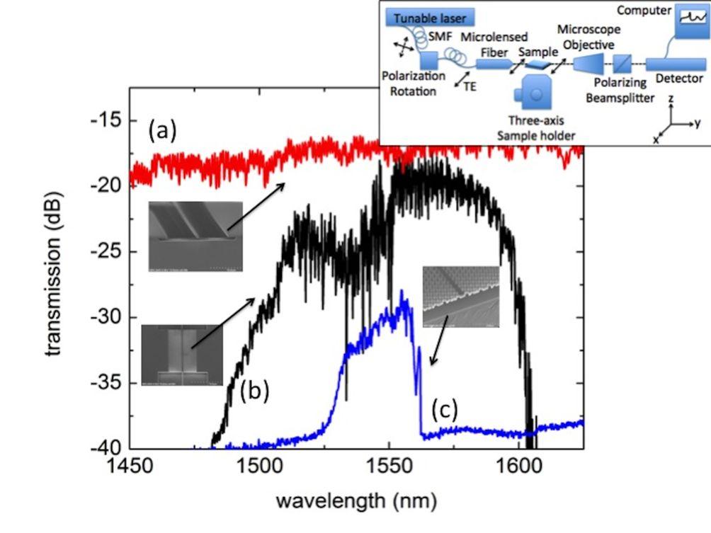
5 calculated for both the SOI and InP-SUI strip waveguides, respectively and we report the eigenvalues here as the effective index, n eff β k 0, for each waveguide. The calculation results, presented in figure 2a and 2b, show that the electric field eigenmode in both cases is very strongly confined to the silicon and InP waveguides with the calculated effective indices of the two types of strip waveguides being n SOI eff 2.56 and n SUI eff Because the effective indices are similar and the confinement is high in both cases, guidance in InP-SUI strip waveguides is very similar to SOI waveguides implying techniques used for effective coupling in SOI should also be well suited for InP access waveguides. Optical transmission of the InP-SUI strip waveguides, with and without an integrated PhC membrane, was obtained using a standard in-plane optical tabletop setup, as shown in the inset of figure 3. The samples were placed on a three-axis stage with the optical input coming from a butt-coupled fiber system consisting of a tunable laser source, polarization rotation optics and a microlensed fiber. The waveguide transmission output was collected by a microscope objective then sent through a polarizing beamsplitter before registering with a photodetector and displayed on a computer. Using the input polarization rotation optics, the input polarization was set to transverse electric (TE), with the electric field oriented in the x- direction indicated in the inset of figure 3, since the PhC membranes were designed to have their waveguide modes defined in their TE band gap. The wavelength range swept with the tunable laser was from 1300 nm to 1600 nm in order to fully characterize the optical passband of the PhC membranes. The optical transmission of two 1 mm long InP-SUI strip waveguides, (a) without and (b) with an integrated 20 μm long PhC-W1 membrane, was collected. The optical transmission of a (c) 500 μm end-to-end PhC-W1 membrane (whose edge facet is shown in figure 1a) was also collected and compared to the two InP-SUI strip waveguides (a) and (b). Figure 3 shows the results of the optical transmission through these three waveguides. The familiar rising and falling edges of PhC optical transmission are seen 5
6 in (b) and (c) depicting the confined optical modes under the light-line and near the slowlight band-edge, respectively. The loss in the InP-SUI strip-membrane system, (b), is about 10 db less than the end-to-end PhC-W1 membrane, (c), even though the end-to-end PhC-W1 membrane is half the length of the InP-SUI strip-membrane system. Such results clearly demonstrate that the top insulator supported InP strip waveguides is a solution for planar optical circuitry that desire to exploit the optical physics of PhC membranes in active media whilst collecting light in an efficient manner to and from fiber optic networks. We have demonstrated a semiconductor-under-insulator technology for designing highly confined single mode strip waveguides in membrane compound semiconductor systems. This technology provides an effective way of fabricating strip waveguides in III-V systems facilitating active planar lightwave circuitry to take advantage of localized PhC membranes without incurring losses associated with long PhC membrane waveguides. The top insulator layer supporting the InP strip waveguide does not limit the transmission band as in the case of tethered supported strip InP waveguides and the active and passive optical material is InP unlike hybrid integrations involving SOI bonded to thin III-V layers. Furthermore, coupling techniques currently in use for SOI systems, such as submicron and inverse couplers, can easily be implemented in this system. The authors gratefully acknowledge the help of Mr. Dan Roth, Mr. Mark Malloy and Ms. Martha E. McCrum. 6
7 FIG. 1. (a) The edge facet of an extended InP PhC-W1 membrane, (b) the edge facet of an InP strip waveguide supported under alumina deposited by ALD, (c) enlarged image of dashed box in (b) showing the InP strip waveguide supported by the conformal ALD alumina layer, (d) InP-SUI strip waveguide interfacing a PhC-W1 membrane structure. Inset is an enlarged image of the area in the dashed box showing the interface between the alumina-supported InP strip waveguide and the PhC-W1 membrane. The arrow in the inset points to a slightly thicker region of the strip waveguide identifying the alumina support layer. FIG. 2. Finite element eigenvalue analysis of (a) silicon on insulator with an effective index of 2.56 and (b) InP under insulator with an effective index of Calculation results show high confinement of the electric field for both SOI and InP-SUI waveguides. Mode propagation is in the z direction as indicated by the axis. FIG. 3. Optical transmission with associated waveguide SEM image of (a) 1 mm InP-SUI strip waveguide, (b) 1 mm InP-SUI strip waveguide with a 20 μm integrated PhC W1 membrane in the middle of the waveguide (as shown in figure 1c) and (c) a 500 μm end-to-end PhC-W1 membrane (where edge facet of this waveguide is shown in figure 1a). Figure inset illustrates the transmission setup used to measure output transmission of the waveguides. 1 H. Altug, D. England, and J. Vuckovic, Nature Physics 2, 484 (2006) 2 T. Sünner, T. Stichel, S.-H. Kwon, T. W. Schlereth, S. Höfling, M. Kamp, and A. Forchel, Appl. Phys. Lett. 92, (2008) 3 D. Dalacu, K. Mnaymneh, V. Sazonova, P. J. Poole, G. C. Aers, J. Lapointe, R. Cheriton, A. J. SpringThorpe and R. L. Williams, Phys. Rev. B 82, (2010) 4 S. J. Dewhurst, D. Granados, D. J. Ellis, A. J. Bennett, R. B. Patel, I. Farrer, D. Anderson, G. A. C. Jones, D. A. Ritchie and A. J. Shields, Appl. Phys. Lett. 96, (2010) 5 K. Mnaymneh, S. Frédérick, D. Dalacu, J. Lapointe, P. J. Poole and R. L. Williams, Opt. Lett. 37, 280 (2012) 6 A. Talneau, K. H. Lee, S. Guilet and I. Sagnes, Appl. Phys. Lett. 92, (2008) 7 G. Roelkens, L. Liu, D. Van Throuhout, R. Baets, R. Nötzel, F. Raineri, I. Sagnes, G. Beaudoin and R. Raj, J. Appl. Phys. 104, (2008) 8 V. I. Tolstikhin, A. Demsmore, K. Pimenov, Y. Logvin, F. Wu, S. Laframboise and S. Grabtchak, J. Lightwave Technol 22, 146 (2004) 9 S. Hughes, L. Ramunno, J. Y. Young and J. E. Sipe, Phys. Rev. Lett. 94, (2005) 10 D. Dai, Y. Tang and J. E. Bowers, Opt. Express 20, (2012) 11 J. A. McCaulley, V. M. Donnelly, M. Vernon and I. Taha, Phys. Rev. B 49, 7408 (1994) 7
8 12 M. D. Groner, F. H. Fabreguette, J. W. Elam and S. M. George, Chem. Mater. 16, 639 (2004) 13 COMSOL Multiphysics J. Jin, The Finite Element Method in Electromagnetics (Willey-IEEE, New York, 2002) 8

9

10
11
Design and fabrication of indium phosphide air-bridge waveguides with MEMS functionality
 Design and fabrication of indium phosphide air-bridge waveguides with MEMS functionality Wing H. Ng* a, Nina Podoliak b, Peter Horak b, Jiang Wu a, Huiyun Liu a, William J. Stewart b, and Anthony J. Kenyon
Optics Communications
 Optics Communications 283 (2010) 3678 3682 Contents lists available at ScienceDirect Optics Communications journal homepage: www.elsevier.com/locate/optcom Ultra-low-loss inverted taper coupler for silicon-on-insulator
Compact hybrid TM-pass polarizer for silicon-on-insulator platform
 Compact hybrid TM-pass polarizer for silicon-on-insulator platform Muhammad Alam,* J. Stewart Aitchsion, and Mohammad Mojahedi Department of Electrical and Computer Engineering, University of Toronto,
CHAPTER 2 POLARIZATION SPLITTER- ROTATOR BASED ON A DOUBLE- ETCHED DIRECTIONAL COUPLER
 CHAPTER 2 POLARIZATION SPLITTER- ROTATOR BASED ON A DOUBLE- ETCHED DIRECTIONAL COUPLER As we discussed in chapter 1, silicon photonics has received much attention in the last decade. The main reason is
Waveguiding in PMMA photonic crystals
 ROMANIAN JOURNAL OF INFORMATION SCIENCE AND TECHNOLOGY Volume 12, Number 3, 2009, 308 316 Waveguiding in PMMA photonic crystals Daniela DRAGOMAN 1, Adrian DINESCU 2, Raluca MÜLLER2, Cristian KUSKO 2, Alex.
Ultracompact Adiabatic Bi-sectional Tapered Coupler for the Si/III-V Heterogeneous Integration
 Ultracompact Adiabatic Bi-sectional Tapered Coupler for the Si/III-V Heterogeneous Integration Qiangsheng Huang, Jianxin Cheng 2, Liu Liu, 2, 2, 3,*, and Sailing He State Key Laboratory for Modern Optical
Two bit optical analog-to-digital converter based on photonic crystals
 Two bit optical analog-to-digital converter based on photonic crystals Binglin Miao, Caihua Chen, Ahmed Sharkway, Shouyuan Shi, and Dennis W. Prather University of Delaware, Newark, Delaware 976 binglin@udel.edu
On-chip Si-based Bragg cladding waveguide with high index contrast bilayers
 On-chip Si-based Bragg cladding waveguide with high index contrast bilayers Yasha Yi, Shoji Akiyama, Peter Bermel, Xiaoman Duan, and L. C. Kimerling Massachusetts Institute of Technology, 77 Massachusetts
Grating coupled photonic crystal demultiplexer with integrated detectors on InPmembrane
 Grating coupled photonic crystal demultiplexer with integrated detectors on InPmembrane F. Van Laere, D. Van Thourhout and R. Baets Department of Information Technology-INTEC Ghent University-IMEC Ghent,
Impact of the light coupling on the sensing properties of photonic crystal cavity modes Kumar Saurav* a,b, Nicolas Le Thomas a,b,
 Impact of the light coupling on the sensing properties of photonic crystal cavity modes Kumar Saurav* a,b, Nicolas Le Thomas a,b, a Photonics Research Group, Ghent University-imec, Technologiepark-Zwijnaarde
Integrated photonic circuit in silicon on insulator for Fourier domain optical coherence tomography
 Integrated photonic circuit in silicon on insulator for Fourier domain optical coherence tomography Günay Yurtsever *,a, Pieter Dumon a, Wim Bogaerts a, Roel Baets a a Ghent University IMEC, Photonics
SUPPLEMENTARY INFORMATION
 Room-temperature continuous-wave electrically injected InGaN-based laser directly grown on Si Authors: Yi Sun 1,2, Kun Zhou 1, Qian Sun 1 *, Jianping Liu 1, Meixin Feng 1, Zengcheng Li 1, Yu Zhou 1, Liqun
Plane wave excitation by taper array for optical leaky waveguide antenna
 LETTER IEICE Electronics Express, Vol.15, No.2, 1 6 Plane wave excitation by taper array for optical leaky waveguide antenna Hiroshi Hashiguchi a), Toshihiko Baba, and Hiroyuki Arai Graduate School of
Design and Analysis of Resonant Leaky-mode Broadband Reflectors
 846 PIERS Proceedings, Cambridge, USA, July 6, 8 Design and Analysis of Resonant Leaky-mode Broadband Reflectors M. Shokooh-Saremi and R. Magnusson Department of Electrical and Computer Engineering, University
Title. Author(s)Fujisawa, Takeshi; Koshiba, Masanori. CitationOptics Letters, 31(1): Issue Date Doc URL. Rights. Type.
Fujisawa, Takeshi; Koshiba, Masanori. CitationOptics Letters, 31(1): Issue Date Doc URL. Rights. Type.") Title Polarization-independent optical directional coupler Author(s)Fujisawa, Takeshi; Koshiba, Masanori CitationOptics Letters, 31(1): 56-58 Issue Date 2006 Doc URL http://hdl.handle.net/2115/948 Rights
Title Polarization-independent optical directional coupler Author(s)Fujisawa, Takeshi; Koshiba, Masanori CitationOptics Letters, 31(1): 56-58 Issue Date 2006 Doc URL http://hdl.handle.net/2115/948 Rights
Propagation loss study of very compact GaAs/AlGaAs substrate removed waveguides
 Propagation loss study of very compact GaAs/AlGaAs substrate removed waveguides JaeHyuk Shin, Yu-Chia Chang and Nadir Dagli * Electrical and Computer Engineering Department, University of California at
InGaAsP photonic band gap crystal membrane microresonators*
 InGaAsP photonic band gap crystal membrane microresonators* A. Scherer, a) O. Painter, B. D Urso, R. Lee, and A. Yariv Caltech, Laboratory of Applied Physics, Pasadena, California 91125 Received 29 May
UC Santa Barbara UC Santa Barbara Previously Published Works
 UC Santa Barbara UC Santa Barbara Previously Published Works Title Compact broadband polarizer based on shallowly-etched silicon-on-insulator ridge optical waveguides Permalink https://escholarship.org/uc/item/959523wq
Figure 1 Basic waveguide structure
 Recent Progress in SOI Nanophotonic Waveguides D. Van Thourhout, P. Dumon, W. Bogaerts, G. Roelkens, D. Taillaert, G. Priem, R. Baets IMEC-Ghent University, Department of Information Technology, St. Pietersnieuwstraat
Hybrid Integration Technology of Silicon Optical Waveguide and Electronic Circuit
 Hybrid Integration Technology of Silicon Optical Waveguide and Electronic Circuit Daisuke Shimura Kyoko Kotani Hiroyuki Takahashi Hideaki Okayama Hiroki Yaegashi Due to the proliferation of broadband services
Silicon Photonic Device Based on Bragg Grating Waveguide
 Silicon Photonic Device Based on Bragg Grating Waveguide Hwee-Gee Teo, 1 Ming-Bin Yu, 1 Guo-Qiang Lo, 1 Kazuhiro Goi, 2 Ken Sakuma, 2 Kensuke Ogawa, 2 Ning Guan, 2 and Yong-Tsong Tan 2 Silicon photonics
Supplementary information for Stretchable photonic crystal cavity with
 Supplementary information for Stretchable photonic crystal cavity with wide frequency tunability Chun L. Yu, 1,, Hyunwoo Kim, 1, Nathalie de Leon, 1,2 Ian W. Frank, 3 Jacob T. Robinson, 1,! Murray McCutcheon,
Index. Cambridge University Press Silicon Photonics Design Lukas Chrostowski and Michael Hochberg. Index.
 absorption, 69 active tuning, 234 alignment, 394 396 apodization, 164 applications, 7 automated optical probe station, 389 397 avalanche detector, 268 back reflection, 164 band structures, 30 bandwidth
A Low-loss Integrated Beam Combiner based on Polarization Multiplexing
 MITSUBISHI ELECTRIC RESEARCH LABORATORIES http://www.merl.com A Low-loss Integrated Beam Combiner based on Polarization Multiplexing Wang, B.; Kojima, K.; Koike-Akino, T.; Parsons, K.; Nishikawa, S.; Yagyu,
Silicon Photonics Technology Platform To Advance The Development Of Optical Interconnects
 Silicon Photonics Technology Platform To Advance The Development Of Optical Interconnects By Mieke Van Bavel, science editor, imec, Belgium; Joris Van Campenhout, imec, Belgium; Wim Bogaerts, imec s associated
This writeup is adapted from Fall 2002, final project report for by Robert Winsor.
 Optical Waveguides in Andreas G. Andreou This writeup is adapted from Fall 2002, final project report for 520.773 by Robert Winsor. September, 2003 ABSTRACT This lab course is intended to give students
Hybrid vertical-cavity laser integration on silicon
 Invited Paper Hybrid vertical-cavity laser integration on Emanuel P. Haglund* a, Sulakshna Kumari b,c, Johan S. Gustavsson a, Erik Haglund a, Gunther Roelkens b,c, Roel G. Baets b,c, and Anders Larsson
Numerical Analysis and Optimization of a Multi-Mode Interference Polarization Beam Splitter
 Numerical Analysis and Optimization of a Multi-Mode Interference Polarization Beam Splitter Y. D Mello*, J. Skoric, M. Hui, E. Elfiky, D. Patel, D. Plant Department of Electrical Engineering, McGill University,
Applications of Cladding Stress Induced Effects for Advanced Polarization Control in Silicon Photonics
 PIERS ONLINE, VOL. 3, NO. 3, 27 329 Applications of Cladding Stress Induced Effects for Advanced Polarization Control in licon Photonics D.-X. Xu, P. Cheben, A. Delâge, S. Janz, B. Lamontagne, M.-J. Picard
Cavity QED with quantum dots in semiconductor microcavities
 Cavity QED with quantum dots in semiconductor microcavities M. T. Rakher*, S. Strauf, Y. Choi, N.G. Stolz, K.J. Hennessey, H. Kim, A. Badolato, L.A. Coldren, E.L. Hu, P.M. Petroff, D. Bouwmeester University
On-chip interrogation of a silicon-on-insulator microring resonator based ethanol vapor sensor with an arrayed waveguide grating (AWG) spectrometer
 spectrometer") On-chip interrogation of a silicon-on-insulator microring resonator based ethanol vapor sensor with an arrayed waveguide grating (AWG) spectrometer Nebiyu A. Yebo* a, Wim Bogaerts, Zeger Hens b,roel Baets
On-chip interrogation of a silicon-on-insulator microring resonator based ethanol vapor sensor with an arrayed waveguide grating (AWG) spectrometer Nebiyu A. Yebo* a, Wim Bogaerts, Zeger Hens b,roel Baets
High-efficiency, high-speed VCSELs with deep oxidation layers
 Manuscript for Review High-efficiency, high-speed VCSELs with deep oxidation layers Journal: Manuscript ID: Manuscript Type: Date Submitted by the Author: Complete List of Authors: Keywords: Electronics
High-efficiency fiber-to-chip grating couplers realized using an advanced CMOS-compatible Silicon-On-Insulator platform
 High-efficiency fiber-to-chip grating couplers realized using an advanced CMOS-compatible Silicon-On-Insulator platform D. Vermeulen, 1, S. Selvaraja, 1 P. Verheyen, 2 G. Lepage, 2 W. Bogaerts, 1 P. Absil,
Loss Reduction in Silicon Nanophotonic Waveguide Micro-bends Through Etch Profile Improvement
 Loss Reduction in Silicon Nanophotonic Waveguide Micro-bends Through Etch Profile Improvement Shankar Kumar Selvaraja, Wim Bogaerts, Dries Van Thourhout Photonic research group, Department of Information
Fully-Etched Grating Coupler with Low Back Reflection
 Fully-Etched Grating Coupler with Low Back Reflection Yun Wang a, Wei Shi b, Xu Wang a, Jonas Flueckiger a, Han Yun a, Nicolas A. F. Jaeger a, and Lukas Chrostowski a a The University of British Columbia,
Selectively-undercut traveling-wave electroabsorption modulators incorporating a p-ingaas contact layer
 Selectively-undercut traveling-wave electroabsorption modulators incorporating a p-ingaas contact layer Matthew M. Dummer, James R. Raring, Jonathan Klamkin, Anna Tauke-Pedretti, and Larry A. Coldren University
Ultracompact and low power optical switch based on silicon. photonic crystals
 Ultracompact and low power optical switch based on silicon photonic crystals Daryl M. Beggs 1, *, Thomas P. White 1, Liam O Faolain 1 and Thomas F. Krauss 1 1 School of Physics and Astronomy, University
Supporting Information: Plasmonic and Silicon Photonic Waveguides
 Supporting Information: Efficient Coupling between Dielectric-Loaded Plasmonic and Silicon Photonic Waveguides Ryan M. Briggs, *, Jonathan Grandidier, Stanley P. Burgos, Eyal Feigenbaum, and Harry A. Atwater,
CHIRPED FIBER BRAGG GRATING (CFBG) BY ETCHING TECHNIQUE FOR SIMULTANEOUS TEMPERATURE AND REFRACTIVE INDEX SENSING
 BY ETCHING TECHNIQUE FOR SIMULTANEOUS TEMPERATURE AND REFRACTIVE INDEX SENSING") CHIRPED FIBER BRAGG GRATING (CFBG) BY ETCHING TECHNIQUE FOR SIMULTANEOUS TEMPERATURE AND REFRACTIVE INDEX SENSING Siti Aisyah bt. Ibrahim and Chong Wu Yi Photonics Research Center Department of Physics,
CHIRPED FIBER BRAGG GRATING (CFBG) BY ETCHING TECHNIQUE FOR SIMULTANEOUS TEMPERATURE AND REFRACTIVE INDEX SENSING Siti Aisyah bt. Ibrahim and Chong Wu Yi Photonics Research Center Department of Physics,
Horizontal single and multiple slot waveguides: optical transmission at λ = 1550 nm
 Horizontal single and multiple slot waveguides: optical transmission at λ = 1550 nm Rong Sun 1 *, Po Dong 2 *, Ning-ning Feng 1, Ching-yin Hong 1, Jurgen Michel 1, Michal Lipson 2, Lionel Kimerling 1 1Department
OPTI510R: Photonics. Khanh Kieu College of Optical Sciences, University of Arizona Meinel building R.626
 OPTI510R: Photonics Khanh Kieu College of Optical Sciences, University of Arizona kkieu@optics.arizona.edu Meinel building R.626 Announcements Homework #3 is due today No class Monday, Feb 26 Pre-record
Ultra-Compact Photonic Crystal Based Water Temperature Sensor
 PHOTONIC SENSORS / Vol. 6, No. 3, 2016: 274 278 Ultra-Compact Photonic Crystal Based Water Temperature Sensor Mahmoud NIKOUFARD *, Masoud KAZEMI ALAMOUTI, and Alireza ADEL Department of Electronics, Faculty
Silicon-based photonic crystal nanocavity light emitters
 Silicon-based photonic crystal nanocavity light emitters Maria Makarova, Jelena Vuckovic, Hiroyuki Sanda, Yoshio Nishi Department of Electrical Engineering, Stanford University, Stanford, CA 94305-4088
Examination Optoelectronic Communication Technology. April 11, Name: Student ID number: OCT1 1: OCT 2: OCT 3: OCT 4: Total: Grade:
 Examination Optoelectronic Communication Technology April, 26 Name: Student ID number: OCT : OCT 2: OCT 3: OCT 4: Total: Grade: Declaration of Consent I hereby agree to have my exam results published on
Photonic Crystal Slot Waveguide Spectrometer for Detection of Methane
 Photonic Crystal Slot Waveguide Spectrometer for Detection of Methane Swapnajit Chakravarty 1, Wei-Cheng Lai 2, Xiaolong (Alan) Wang 1, Che-Yun Lin 2, Ray T. Chen 1,2 1 Omega Optics, 10306 Sausalito Drive,
Tunable Color Filters Based on Metal-Insulator-Metal Resonators
 Chapter 6 Tunable Color Filters Based on Metal-Insulator-Metal Resonators 6.1 Introduction In this chapter, we discuss the culmination of Chapters 3, 4, and 5. We report a method for filtering white light
Analysis of characteristics of bent rib waveguides
 D. Dai and S. He Vol. 1, No. 1/January 004/J. Opt. Soc. Am. A 113 Analysis of characteristics of bent rib waveguides Daoxin Dai Centre for Optical and Electromagnetic Research, Joint Laboratory of Optical
Integrated Focusing Photoresist Microlenses on AlGaAs Top-Emitting VCSELs
 Integrated Focusing Photoresist Microlenses on AlGaAs Top-Emitting VCSELs Andrea Kroner We present 85 nm wavelength top-emitting vertical-cavity surface-emitting lasers (VCSELs) with integrated photoresist
Realization of Polarization-Insensitive Optical Polymer Waveguide Devices
 644 Realization of Polarization-Insensitive Optical Polymer Waveguide Devices Kin Seng Chiang,* Sin Yip Cheng, Hau Ping Chan, Qing Liu, Kar Pong Lor, and Chi Kin Chow Department of Electronic Engineering,
E LECTROOPTICAL(EO)modulatorsarekeydevicesinoptical
modulatorsarekeydevicesinoptical") 286 JOURNAL OF LIGHTWAVE TECHNOLOGY, VOL. 26, NO. 2, JANUARY 15, 2008 Design and Fabrication of Sidewalls-Extended Electrode Configuration for Ridged Lithium Niobate Electrooptical Modulator Yi-Kuei Wu,
286 JOURNAL OF LIGHTWAVE TECHNOLOGY, VOL. 26, NO. 2, JANUARY 15, 2008 Design and Fabrication of Sidewalls-Extended Electrode Configuration for Ridged Lithium Niobate Electrooptical Modulator Yi-Kuei Wu,
OPTICAL MODE STUDY OF GALIUM NITRIDE BASED LASER DIODES. A Senior Project presented to. the Faculty of the ELECTICAL ENGINEERING DEPARTMENT
 OPTICAL MODE STUDY OF GALIUM NITRIDE BASED LASER DIODES A Senior Project presented to the Faculty of the ELECTICAL ENGINEERING DEPARTMENT California Polytechnic State University, San Luis Obispo In Partial
Robert G. Hunsperger. Integrated Optics. Theory and Technology. Sixth Edition. 4ü Spri rineer g<
 Robert G. Hunsperger Integrated Optics Theory and Technology Sixth Edition 4ü Spri rineer g< 1 Introduction 1 1.1 Advantages of Integrated Optics 2 1.1.1 Comparison of Optical Fibers with Other Interconnectors
Long-Wavelength Waveguide Photodiodes for Optical Subscriber Networks
 Long-Wavelength Waveguide Photodiodes for Optical Subscriber Networks by Masaki Funabashi *, Koji Hiraiwa *, Kazuaki Nishikata * 2, Nobumitsu Yamanaka *, Norihiro Iwai * and Akihiko Kasukawa * Waveguide
CMOS Digital Integrated Circuits Lec 2 Fabrication of MOSFETs
 CMOS Digital Integrated Circuits Lec 2 Fabrication of MOSFETs 1 CMOS Digital Integrated Circuits 3 rd Edition Categories of Materials Materials can be categorized into three main groups regarding their
Lecture: Integration of silicon photonics with electronics. Prepared by Jean-Marc FEDELI CEA-LETI
 Lecture: Integration of silicon photonics with electronics Prepared by Jean-Marc FEDELI CEA-LETI Context The goal is to give optical functionalities to electronics integrated circuit (EIC) The objectives
Monolithic integration of erbium-doped amplifiers with silicon waveguides
 Monolithic integration of erbium-doped amplifiers with silicon waveguides Laura Agazzi, 1* Jonathan D. B. Bradley, 1 Feridun Ay, 1 Gunther Roelkens, 2 Roel Baets, 2 Kerstin Wörhoff, 1 and Markus Pollnau
InP-based Waveguide Photodetector with Integrated Photon Multiplication
 InP-based Waveguide Photodetector with Integrated Photon Multiplication D.Pasquariello,J.Piprek,D.Lasaosa,andJ.E.Bowers Electrical and Computer Engineering Department University of California, Santa Barbara,
Optimization of supercontinuum generation in photonic crystal fibers for pulse compression
 Optimization of supercontinuum generation in photonic crystal fibers for pulse compression Noah Chang Herbert Winful,Ted Norris Center for Ultrafast Optical Science University of Michigan What is Photonic
AWG OPTICAL DEMULTIPLEXERS: FROM DESIGN TO CHIP. D. Seyringer
 AWG OPTICAL DEMULTIPLEXERS: FROM DESIGN TO CHIP D. Seyringer Research Centre for Microtechnology, Vorarlberg University of Applied Sciences, Hochschulstr. 1, 6850 Dornbirn, Austria, E-mail: dana.seyringer@fhv.at
Long-Working-Distance Grating Coupler for Integrated Optical Devices
 Long-Working-Distance Grating Coupler for Integrated Optical Devices Volume 8, Number 1, February 2016 C. J. Oton DOI: 10.1109/JPHOT.2015.2511098 1943-0655 Ó 2015 IEEE Long-Working-Distance Grating Coupler
LASER &PHOTONICS REVIEWS
 LASER &PHOTONICS REPRINT Laser Photonics Rev., L1 L5 (2014) / DOI 10.1002/lpor.201300157 LASER & PHOTONICS Abstract An 8-channel hybrid (de)multiplexer to simultaneously achieve mode- and polarization-division-(de)multiplexing
Nanofluidic Diodes based on Nanotube Heterojunctions
 Supporting Information Nanofluidic Diodes based on Nanotube Heterojunctions Ruoxue Yan, Wenjie Liang, Rong Fan, Peidong Yang 1 Department of Chemistry, University of California, Berkeley, CA 94720, USA
Influence of dielectric substrate on the responsivity of microstrip dipole-antenna-coupled infrared microbolometers
 Influence of dielectric substrate on the responsivity of microstrip dipole-antenna-coupled infrared microbolometers Iulian Codreanu and Glenn D. Boreman We report on the influence of the dielectric substrate
Monolithically integrated InGaAs nanowires on 3D. structured silicon-on-insulator as a new platform for. full optical links
 Monolithically integrated InGaAs nanowires on 3D structured silicon-on-insulator as a new platform for full optical links Hyunseok Kim 1, Alan C. Farrell 1, Pradeep Senanayake 1, Wook-Jae Lee 1,* & Diana.
SUPPLEMENTARY INFORMATION DOI: /NPHOTON
 Contents Simulations... 1 Purcell factor estimation... 4 Fabrication... 4 Characterization results... 5 References... 7 Simulations The resonant modes and gain thresholds were found using COMSOL s -D and
2D silicon-based surface-normal vertical cavity photonic crystal waveguide array for high-density optical interconnects
 2D silicon-based surface-normal vertical cavity photonic crystal waveguide array for high-density optical interconnects JaeHyun Ahn a, Harish Subbaraman b, Liang Zhu a, Swapnajit Chakravarty b, Emanuel
Flip chip Assembly with Sub-micron 3D Re-alignment via Solder Surface Tension
 Flip chip Assembly with Sub-micron 3D Re-alignment via Solder Surface Tension Jae-Woong Nah*, Yves Martin, Swetha Kamlapurkar, Sebastian Engelmann, Robert L. Bruce, and Tymon Barwicz IBM T. J. Watson Research
Cost-effective CMOS-compatible grating couplers with backside metal mirror and 69% coupling efficiency
 Cost-effective CMOS-compatible grating couplers with backside metal mirror and 69% coupling efficiency Wissem Sfar Zaoui, 1,* María Félix Rosa, 1 Wolfgang Vogel, 1 Manfred Berroth, 1 Jörg Butschke, 2 and
Heterogeneously Integrated Microwave Signal Generators with Narrow- Linewidth Lasers
 Heterogeneously Integrated Microwave Signal Generators with Narrow- Linewidth Lasers John E. Bowers, Jared Hulme, Tin Komljenovic, Mike Davenport and Chong Zhang Department of Electrical and Computer Engineering
SUPPLEMENTARY INFORMATION
 Silver permittivity used in the simulations Silver permittivity values are obtained from Johnson & Christy s experimental data 31 and are fitted with a spline interpolation in order to estimate the permittivity
High-yield Fabrication Methods for MEMS Tilt Mirror Array for Optical Switches
 : MEMS Device Technologies High-yield Fabrication Methods for MEMS Tilt Mirror Array for Optical Switches Joji Yamaguchi, Tomomi Sakata, Nobuhiro Shimoyama, Hiromu Ishii, Fusao Shimokawa, and Tsuyoshi
Development of Vertical Spot Size Converter (SSC) with Low Coupling Loss Using 2.5%Δ Silica-Based Planar Lightwave Circuit
 with Low Coupling Loss Using 2.5%Δ Silica-Based Planar Lightwave Circuit") Development of Vertical Spot Size Converter (SSC) with Low Coupling Loss Using 2.5%Δ Silica-Based Planar Lightwave Circuit Yasuyoshi Uchida *, Hiroshi Kawashima *, and Kazutaka Nara * Recently, new planar
Development of Vertical Spot Size Converter (SSC) with Low Coupling Loss Using 2.5%Δ Silica-Based Planar Lightwave Circuit Yasuyoshi Uchida *, Hiroshi Kawashima *, and Kazutaka Nara * Recently, new planar
Integrated High Speed VCSELs for Bi-Directional Optical Interconnects
 Integrated High Speed VCSELs for Bi-Directional Optical Interconnects Volodymyr Lysak, Ki Soo Chang, Y ong Tak Lee (GIST, 1, Oryong-dong, Buk-gu, Gwangju 500-712, Korea, T el: +82-62-970-3129, Fax: +82-62-970-3128,
Tuning of Silicon-On-Insulator Ring Resonators with Liquid Crystal Cladding using the Longitudinal Field Component
 Tuning of Silicon-On-Insulator Ring Resonators with Liquid Crystal Cladding using the Longitudinal Field Component Wout De Cort, 1,2, Jeroen Beeckman, 2 Richard James, 3 F. Anibal Fernández, 3 Roel Baets
Design and Simulation of Optical Power Splitter By using SOI Material
 J. Pure Appl. & Ind. Phys. Vol.3 (3), 193-197 (2013) Design and Simulation of Optical Power Splitter By using SOI Material NAGARAJU PENDAM * and C P VARDHANI 1 * Research Scholar, Department of Physics,
Optically reconfigurable balanced dipole antenna
 Loughborough University Institutional Repository Optically reconfigurable balanced dipole antenna This item was submitted to Loughborough University's Institutional Repository by the/an author. Citation:
Microphotonics Readiness for Commercial CMOS Manufacturing. Marco Romagnoli
 Microphotonics Readiness for Commercial CMOS Manufacturing Marco Romagnoli MicroPhotonics Consortium meeting MIT, Cambridge October 15 th, 2012 Passive optical structures based on SOI technology Building
64 Channel Flip-Chip Mounted Selectively Oxidized GaAs VCSEL Array
 64 Channel Flip-Chip Mounted Selectively Oxidized GaAs VCSEL Array 69 64 Channel Flip-Chip Mounted Selectively Oxidized GaAs VCSEL Array Roland Jäger and Christian Jung We have designed and fabricated
High-speed Ge photodetector monolithically integrated with large cross silicon-on-insulator waveguide
 [ APPLIED PHYSICS LETTERS ] High-speed Ge photodetector monolithically integrated with large cross silicon-on-insulator waveguide Dazeng Feng, Shirong Liao, Roshanak Shafiiha. etc Contents 1. Introduction
Luminous Equivalent of Radiation
 Intensity vs λ Luminous Equivalent of Radiation When the spectral power (p(λ) for GaP-ZnO diode has a peak at 0.69µm) is combined with the eye-sensitivity curve a peak response at 0.65µm is obtained with
Large Scale Silicon Photonic MEMS Switch
 Large Scale Silicon Photonic MEMS Switch Sangyoon Han Electrical Engineering and Computer Sciences University of California at Berkeley Technical Report No. UCB/EECS-2015-40 http://www.eecs.berkeley.edu/pubs/techrpts/2015/eecs-2015-40.html
SUPPLEMENTARY INFORMATION
 Transfer printing stacked nanomembrane lasers on silicon Hongjun Yang 1,3, Deyin Zhao 1, Santhad Chuwongin 1, Jung-Hun Seo 2, Weiquan Yang 1, Yichen Shuai 1, Jesper Berggren 4, Mattias Hammar 4, Zhenqiang
Semiconductor Optical Active Devices for Photonic Networks
 UDC 621.375.8:621.38:621.391.6 Semiconductor Optical Active Devices for Photonic Networks VKiyohide Wakao VHaruhisa Soda VYuji Kotaki (Manuscript received January 28, 1999) This paper describes recent
Reduction in Sidelobe Level in Ultracompact Arrayed Waveguide Grating Demultiplexer Based on Si Wire Waveguide
 Reduction in Sidelobe Level in Ultracompact Arrayed Waveguide Grating Demultiplexer Based on Si Wire Waveguide Fumiaki OHNO, Kosuke SASAKI, Ayumu MOTEGI and Toshihiko BABA Department of Electrical and
FABRICATION OF CMOS INTEGRATED CIRCUITS. Dr. Mohammed M. Farag
 FABRICATION OF CMOS INTEGRATED CIRCUITS Dr. Mohammed M. Farag Outline Overview of CMOS Fabrication Processes The CMOS Fabrication Process Flow Design Rules Reference: Uyemura, John P. "Introduction to
Polarization Control of VCSELs
 Polarization Control of VCSELs Johannes Michael Ostermann and Michael C. Riedl A dielectric surface grating has been used to control the polarization of VCSELs. This grating is etched into the surface
Part 5-1: Lithography
 Part 5-1: Lithography Yao-Joe Yang 1 Pattern Transfer (Patterning) Types of lithography systems: Optical X-ray electron beam writer (non-traditional, no masks) Two-dimensional pattern transfer: limited
Confined Photonic Modes in the Fabry-Pérot Based Photonic Crystal Nanobeam Cavity Structures with Mixed Tapered Air- Holes and Curved-Wall Cavity
 American Journal of Engineering Research (AJER) e-issn : 2320-0847 p-issn : 2320-0936 Volume-03, Issue-02, pp-30-35 www.ajer.org Research Paper Open Access Confined Photonic Modes in the Fabry-Pérot Based
Optomechanical coupling in photonic crystal supported nanomechanical waveguides
 Optomechanical coupling in photonic crystal supported nanomechanical waveguides W.H.P. Pernice 1, Mo Li 1 and Hong X. Tang 1,* 1 Departments of Electrical Engineering, Yale University, New Haven, CT 06511,
Silicon photonic devices based on binary blazed gratings
 Silicon photonic devices based on binary blazed gratings Zhiping Zhou Li Yu Optical Engineering 52(9), 091708 (September 2013) Silicon photonic devices based on binary blazed gratings Zhiping Zhou Li Yu
SELF COLLIMATION IN PILLAR TYPE PHOTONIC CRYSTAL USING COMSOL
 SELF COLLIMATION IN PILLAR TYPE PHOTONIC CRYSTAL USING COMSOL S.Hemalatha 1, K.Shanthalakshmi 2 1 ME Communication Systems Department of ECE Adhiyamaan College Of Engineering, Hosur, India 2 Associate
Vanishing Core Fiber Spot Size Converter Interconnect (Polarizing or Polarization Maintaining)
") Vanishing Core Fiber Spot Size Converter Interconnect (Polarizing or Polarization Maintaining) The Go!Foton Interconnect (Go!Foton FSSC) is an in-fiber, spot size converting interconnect for convenient
Vanishing Core Fiber Spot Size Converter Interconnect (Polarizing or Polarization Maintaining) The Go!Foton Interconnect (Go!Foton FSSC) is an in-fiber, spot size converting interconnect for convenient
InP-based waveguide photodiodes heterogeneously integrated on silicon-oninsulator for photonic microwave generation
 InP-based waveguide photodiodes heterogeneously integrated on silicon-oninsulator for photonic microwave generation Andreas Beling, 1,* Allen S. Cross, 1 Molly Piels, 2 Jon Peters, 2 Qiugui Zhou, 1 John
Printing Beyond srgb Color Gamut by. Mimicking Silicon Nanostructures in Free-Space
 Supporting Information for: Printing Beyond srgb Color Gamut by Mimicking Silicon Nanostructures in Free-Space Zhaogang Dong 1, Jinfa Ho 1, Ye Feng Yu 2, Yuan Hsing Fu 2, Ramón Paniagua-Dominguez 2, Sihao
Heterogeneous Integration of Silicon and AlGaInAs for a Silicon Evanescent Laser
 Invited Paper Heterogeneous Integration of Silicon and AlGaInAs for a Silicon Evanescent Laser Alexander W. Fang a, Hyundai Park a, Richard Jones b, Oded Cohen c, Mario J. Paniccia b, and John E. Bowers
Printed Large-Area Single-Mode Photonic Crystal Bandedge Surface- Emitting Lasers on Silicon
 Printed Large-Area Single-Mode Photonic Crystal Bandedge Surface- Emitting Lasers on Silicon Deyin Zhao a, Shihchia Liu a, Hongjun Yang, Zhenqiang Ma, Carl Reuterskiöld-Hedlund 3, Mattias Hammar 3, and
High-Q surface plasmon-polariton microcavity
 Chapter 5 High-Q surface plasmon-polariton microcavity 5.1 Introduction As the research presented in this thesis has shown, microcavities are ideal vehicles for studying light and matter interaction due
Reduction in Sidelobe Level in Ultracompact Arrayed Waveguide Grating Demultiplexer Based on Si Wire Waveguide
 Japanese Journal of Applied Physics Vol. 45, No. 8A, 26, pp. 6126 6131 #26 The Japan Society of Applied Physics Photonic Crystals and Related Photonic Nanostructures Reduction in Sidelobe Level in Ultracompact
Multiple wavelength resonant grating filters at oblique incidence with broad angular acceptance
 Multiple wavelength resonant grating filters at oblique incidence with broad angular acceptance Andrew B. Greenwell, Sakoolkan Boonruang, M.G. Moharam College of Optics and Photonics - CREOL, University
Introduction Fundamentals of laser Types of lasers Semiconductor lasers
 ECE 5368 Introduction Fundamentals of laser Types of lasers Semiconductor lasers Introduction Fundamentals of laser Types of lasers Semiconductor lasers How many types of lasers? Many many depending on