RF-LAMBDA LEADER OF RF BROADBAND SOLUTIONS
|
|
|
- Randolph Rose
- 5 years ago
- Views:
Transcription

 13 15 12 14 dbm Saturated Output Power (Psat) 16.5 15.5 dbm Output Third Order Intercept (OIP3) 25.")
1 Ultra Wide Band Low Noise Amplifier 0.01GHz~10GHz Electrical Specifications, TA = 25, Vcc = 12V Features Gain: 28dB Typical Noise Figure: 2.5dB Typical High P1dB: 15dBm Typical Supply Voltage: 12V Parameter Min Typ Max Min Typ Max Units Frequency Range GHz Gain db Gain Flatness ±2.0 ±2.5 ±1.0 ±2.0 db Gain Variation Over Temperature (-45 ~85 ) ±1.0 ±1.0 db Noise Figure db Input VSWR : 1 Output VSWR : 1 Output 1dB Compression Point (P1dB) dbm Saturated Output Power (Psat) dbm Output Third Order Intercept (OIP3) dbm Supply Current (Vcc=12V) ma Isolation S db Weight 1.06 Ounces Impedance 50 Ohms Input / Output Connectors Finish Material Package Sealing Typical Applications Wireless Infrastructure RF Microwave & VSAT Military & Aerospace Test Instrument SMA - Female Standard: Gold 40 micron; Nickel 220 micron thickness Option: Gold 80 micron; Nickel 180 micron thickness Aluminum Epoxy Sealed (Standard) Hermetically Sealed (Optional)
2 Absolute Maximum Ratings Operating Voltage 15V RF Input Power -10dBm Biasing Up Procedure Step 1 Connect Ground Pin Step 2 Connect input and output Step 3 Connect 12V biasing Power OFF Procedure Environmental Specifications and Test Standards Step 1 Step 2 Step 3 Parameter Standard Description Operational Temperature MIL-STD ~85 Storage Temperature -55 ~125 Thermal Shock Random Vibration Electrical & Temperature Burn In Shock Altitude Hermetically Sealed (Optional) MIL-STD-883 Turn off 12V biasing Remove RF connection Remove Ground. 1 Hour@ (5 Cycles) Acceleration Spectral Density 6 (m/s) Total 92.6 RMS Temperature 85 for 72 Hours 1. Weight >20g, 50g half sine wave for 11ms, Speed variation 3.44m/s 2. Weight <=20g, 100g Half sine wave for 6ms, Speed variation 3.75m/s 3. Total 18 times (6 directions, 3 repetitions per direction). Standard: 30,000 Ft (Epoxy Sealed Controlled Environment) Optional: Hermetically Sealed (60,000 ft. 1.0 PSI min) MIL-STD-883 (For Hermetically Sealed Units)


3 Typical Performance Plots Input Output Input Output

 Noise Figure(0.")
4 RF-LAMBDA Input Output Gain vs. Output Power P1dB vs. Frequency Output Third Order Intercept (OIP3) Noise Figure(0.2-4GHz)

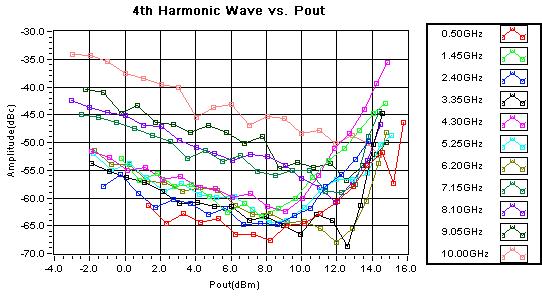
5 Noise Figure(4-10GHz) 2nd Harmonic Wave Output Power 3rd Harmonic Wave Output Power 4th Harmonic Wave Output Power
6 8.5 [0.33] 15 [0.59] 13 [0.51] 17 [0.67] 20 [0.79] 30 [1.18] 8.5 [0.33] 8.7 [0.34] 3.5 [0.14] 12 [0.47] 15 [0.59] 27 [1.06] 18.5 [0.73] RF-LAMBDA Outline Drawing: All Dimensions in mm [inches] 12 [0.47] 8.7 [0.34] Heat Sink required during operation(sold Separately) Ordering Information IN 26.6 [1.05] 48 [1.89] 36 [1.42] RF-Lambda F: GHz SN:XXXXXXXXXXX 12V GND 21.4 [0.84] Part No. ECCN Description OUT 4-2.2[0.09] THRU 28 [1.10] IN 4-3.2[0.126] THRU 92 [3.62] 80 [3.15] RF-Lambda F: GHz SN:XXXXXXXXXXX 12V GND OUT 4 [0.16] 5.9 [0.23] 12.5 [0.49] Including Heat sink EAR GHz Low Noise Amplifier Important Notice The information contained herein is believed to be reliable. RF-Lambda makes no warranties regarding the information contained herein. RF-Lambda assumes no responsibility or liability whatsoever for any of the information contained herein. RF-Lambda assumes no responsibility or liability whatsoever for the use of the information contained herein. The information contained herein is provided "AS IS, WHERE IS" and with all faults, and the entire risk associated with such information is entirely with the user. All information contained herein is subject to change without notice. Customers should obtain and verify the latest relevant information before placing orders for RF-Lambda products. The information contained herein or any use of such information does not grant, explicitly or implicitly, to any party any patent rights, licenses, or any other intellectual property rights, whether with regard to such information itself or anything described by such information. RF-Lambda products are not warranted or authorized for use as critical components in medical, life-saving, or life sustaining applications, or other applications where a failure would reasonably be expected to cause severe personal injury or death.
RF-LAMBDA LEADER OF RF BROADBAND SOLUTIONS
 Voltage Control Phase Shifter 2-4GHz Features Wide Band Operation 2-4GHz 360 Phase Shift Low Insertion Loss and Low Phase Error Singe Control Operation Customization available upon request Electrical Specifications,
RF-LAMBDA LEADER OF RF BROADBAND SOLUTIONS
 Absorptive Voltage Controlled Attenuator 4-8GHz Features Wide Band Operation 4-8GHz Wide Attenuation Range 30dB Absorptive Topology Singe Control Operation Electrical Specifications, T A = 25 C Description
RF-LAMBDA LEADER OF RF BROADBAND SOLUTIONS
 Ultra Wide Band Power Amplifier 0.7GHz ~ 6GHz Features Gain: 35dB typical Output power 38dBm typical High P1dB: 35 dbm Full Band Supply Voltage: 28V 50 Ohm Matched Electrical Specifications, T A = 25⁰C,
RF-LAMBDA LEADER OF RF BROADBAND SOLUTIONS
 LEADER OF RF BROADBAND SOLTIONS Low Noise Amplifier.~. RLNAGG Electrical Specifications, TA = + C, Vcc = +V Features Gain: Typical Noise Figure:. Typical P Output Power: + m Typical Supply Voltage: + V
RF-LAMBDA LEADER OF RF BROADBAND SOLUTIONS
 RF-LAMBDA LEADER OF RF BROADBAND SOLTIONS RPNAGGA W Front Over Drive Protected LNA ltra Wide Band Low Noise Amplifier ~ Electrical Specifications, TA = ⁰C, Vcc = V Features Gain: Typical Noise Figure:.
RF-LAMBDA LEADER OF RF BROADBAND SOLUTIONS
 Absorptive Coaxial SP3T Switch 0.5-50GHz Electrical Specifications, T A = +25 C, Vdd = +5V/-5V, TTL = 0 / +5V Description PN: SP3T Absorptive Switch Low Power Cold Switching Parameter Min Typ Max Min Typ
RF-LAMBDA LEADER OF RF BROADBAND SOLUTIONS
 Reflective Coaxial SP2T Switch 50 700MHz Electrical Specifications, TA = +25 C, Vdd = +5V/-28V, TTL = 0 / +5V Description Features Wide Band Operation 50-700MHz TTL compatible driver included Fast Switching
RF-LAMBDA LEADER OF RF BROADBAND SOLUTIONS
 Electrical Specifications, TA =, Vcc = V ltra Wide Band Low Noise Amplifier.~ Features Gain: Typical Noise Figure:. Typical Output power m typical High P: m Full Band Supply Voltage: V Parameter in. Typ.
RF-LAMBDA LEADER OF RF BROADBAND SOLUTIONS
 Electrical Specifications, T A =25 Ultra Wide Band Low Noise Amplifier AC 110V/220V 0.01-20GHz Parameters Min. Typ. Max. Min. Typ. Max. Units Frequency Range 0.01 10 10 20 GHz Gain 28 30 26 28 db Gain
5W Ultra Wide Band Power Amplifier 2-18GHz. Parameter Min. Typ. Max. Min. Typ. Max. Units
 7-3 RF-LAMBDA 5W Ultra Wide Band Power Amplifier 2-18GHz Features Wideband Solid State Power Amplifier Psat: + 37dBm Gain: 35 db Supply Voltage: +24V Electrical Specifications, T A = +25⁰C, Vcc = +24V
RF-LAMBDA LEADER OF RF BROADBAND SOLUTIONS
 LEADER OF RF BROADBAND SOLTIONS Wideband Low Noise Amplifier.~ RLNAMGB Features Gain: Typical Noise Figure:. Typical Output P: m Typical Supply Voltage: V Ohm Matched Electrical Specifications, TA = ⁰C,
Ultra Wide Band Low Noise Amplifier GHz. Electrical Specifications, TA = +25⁰C, With Vg= -5V, Vcc = +4V ~ +7V, 50 Ohm System
 Ultra Wide Band Low Noise Amplifier 0.5 46GHz Parameter Min. Typ. Max. Min. Typ. Max. Units Frequency Range 0.5 20 20 46 GHz Gain 13 13 db Gain Variation Over Temperature (-45 ~ +85) ±3 ±2 db Noise Figure
8W Wide Band Power Amplifier 1GHz~22GHz
 8W Wide Band Power Amplifier 1GHz~22GHz Features Wideband Solid State Power Amplifier Gain: 50 db Typical Psat: +39 dbm Supply Voltage: +36V Electrical Specifications, T A = +25⁰C Typical Applications
30W Solid State High Power Amplifier 2-6 GHz. Parameter Min. Typ. Max. Min. Typ. Max. Units
 7-3 RF-LAMBDA 30W Solid State High Power Amplifier 2-6 GHz Features Wideband Solid State Power Amplifier Psat: +45dBm Gain: 50dB Supply Voltage: +36V Electrical Specifications, T A = +25⁰C, Vcc = +36V
RF-LAMBDA LEADER OF RF BROADBAND SOLUTIONS
 Ultra Wide Band Low Noise Amplifier 0.01GHz~30GHz Electrical Specifications, TA = 25⁰C Features Gain: 36 Typical Noise Figure: 3.5 Typical P1 Output Power: 28m Typical Supply Voltage: AC110V~220V Typical
RF-LAMBDA LEADER OF RF BROADBAND SOLUTIONS
 LEADER OF RF BROADBAND SOLTIONS ltra Wide Band Low Noise Amplifier.~ Electrical Specifications, TA = ⁰C, Vcc = V Parameters Min. Typ. Max. Min. Typ. Max. nits Frequency Range... Gain Gain Flatness ±. ±.
RF-LAMBDA LEADER OF RF BROADBAND SOLUTIONS
 Wide Band Power Amplifier.~ Electrical Specifications, TA = ⁰C, Vcc = V Features Gain: Typical Noise Figure:. Typical Output P: m Typical Supply Voltage: V Ohm Matched Typical Applications Wireless Infrastructure
RF-LAMBDA LEADER OF RF BROADBAND SOLUTIONS
 50W Broadband High Power Amplifier Module 500 2500MHz Electrical Specifications, T A = +25⁰C, Vdd = +28V Features Ultra-broadband Amplifier Module Small and lightweight Supply Voltage: +28V Parameter Min.
4W Ultra Wide Band Power Amplifier 0.1GHz~22GHz
 4W Ultra Wide Band Power Amplifier 0.1GHz~22GHz Features Wideband Solid State Power Amplifier Gain: 40 db Typical Psat: +37 dbm Typical Noise Figure: 3dB Typical Supply Voltage: +24V (-NP) / +36V (-WP)
RF-LAMBDA LEADER OF RF BROADBAND SOLUTIONS
 100W Coaxial Microwave Power Amplifier 20MHz~520MHz Features Small signal open loop gain: 50dB Output power 100W typical Electrical Specifications, T A = +25 C Typical Applications Suitable for RFI, EMC
Parameter Min. Typ. Max. Min. Typ. Max. Units
 Electrical Specifications, TA = 25 C, With Vcc = 12V, 50 Ohm System Feature Gain: 36 db Noise Figure: 3.0dB P1dB Output Power: 10dB m full band Supply Voltage: 12V @185mA 50 Ohm Matched Input / Output
RF-LAMBDA LEADER OF RF BROADBAND SOLUTIONS
 LEADER OF RF BROADBAND SOLTIONS Wideband Solid State Power Amplifier - Features Gain: typical Output power +m typical High P: + m Full Band Supply Voltage: +V Ohm Matched RFLPAGGA Electrical Specifications,
30W Wideband Solid State Power Amplifier 6-12GHz. Parameter Min. Typ. Max. Min. Typ. Max. Units
 7-3 RF-LAMBDA 30W Wideband Solid State Power Amplifier 6-12GHz Electrical Specifications, TA = +25⁰C, Vdd = +36V Parameter Min. Typ. Max. Min. Typ. Max. Units Frequency Range 6 9 10 12 GHz Gain 60 55 db
100W Wide Band Power Amplifier 6GHz~18GHz. Parameter Min. Typ. Max. Min. Typ. Max. Units. Frequency Range GHz Gain db
 100W Wide Band Power Amplifier 6GHz~18GHz Features Wideband Solid State Power Amplifier Psat: +50dBm Gain: 75 db Typical Supply Voltage: +48V On board microprocessor driven bias controller. Electrical
RF-LAMBDA LEADER OF RF BROADBAND SOLUTIONS
 Reflective Coaxial SP2T Switch DC - 6 Electrical Specifications, TA = +25 C, Vcc +5V, TTL= 0 / +5V Description Features Wide Band Operation DC-6 TTL compatible driver included Fast Switching Speed Low
RF-LAMBDA LEADER OF RF BROADBAND SOLUTIONS
 Wide Band High Power Solid State Power Amplifier 2GHz~6GHz Electrical Specifications, TA = +25⁰C, Vcc = +28V Features Gain: 42 db min Output power +47dBm typical High P1dB: +45dB m Full Band Supply Voltage:
RF-LAMBDA LEADER OF RF BROADBAND SOLUTIONS
 Wide Band Power Amplifier 18~45 Features Gain: 35 typical Output power +26m typical High P1: +24 m Full Band Supply Voltage: +12V 50 Ohm Matched Input / Output The photo is only to show the package type.
RF-LAMBDA LEADER OF RF BROADBAND SOLUTIONS
 80W Broadband High Power Amplifier Module 20-1000MHz Electrical Specifications, T A = +25⁰C, VDD = +28V Features Broadband High Power High Efficiency Great Linearity Small Size & Light Weight Low Distortion
RF-LAMBDA LEADER OF RF BROADBAND SOLUTIONS
 Ultra Wide Band Low Noise Amplifier AC 1V/2V 0.0~ Electrical Specifications, T A =2 Parameters Min. Typ. Max. Min. Typ. Max. Units Frequency Range 0.01 1 1 3 GHz Gain 33 36 33 36 db Gain Flatness ±1. ±1.0
20W Solid State Power Amplifier 26.2GHz~34GHz. Parameter Min. Typ. Max. Min. Typ. Max. Units. Frequency Range GHz.
 20W Solid State Power Amplifier 26.2GHz~34GHz Features Wideband Solid State Power Amplifier Gain: 65dB Typical Psat: +43dBm Typical Supply : +24V Electrical Specifications, T A = +25⁰C, Vcc = +24V Typical
2W Ultra Wide Band Power Amplifier 0.2GHz~35GHz. Parameter Min. Typ. Max. Min. Typ. Max. Min. Typ. Max. Units. Frequency Range
 2W Ultra Wide Band Power Amplifier 0.2GHz~35GHz Features Wideband Solid State Power Amplifier Gain: 37dB Typical Psat 35dBm Typical Electrical Specifications, TA = +25⁰C, Vcc = +12V. Parameter Min. Typ.
RF-LAMBDA LEADER OF RF BROADBAND SOLUTIONS
 LEADER OF RF BROADBAND SOLTIONS Absorptive Coaxial SP2T Switch.2 ~ Features Wide Band Operation.2- TTL compatible driver included Fast Switching Speed Low Insertion Loss and High Isolation Customization
RF-LAMBDA LEADER OF RF BROADBAND SOLUTIONS
 Absorptive Coaxial SP3T Switch 8-43.5 Electrical Specifications, T A = +25 C, Vdd = +5V/-5V, TTL = 0 / +5V Description PN: SP3T Absorptive Switch Low Power Cold Switching Parameters Min. Typ. Max. Min.
20W Solid State Power Amplifier 6-18GHz. Parameter Min. Typ. Max. Min. Typ. Max. Units
 7-3 RF-LAMBDA 20W Solid State Power Amplifier 6-18GHz Electrical Specifications, TA = +25⁰C Vcc = +36V Features Psat: + 43.5dBm Gain: 51 db Supply Voltage: +36V 50 Ohm Matched Short Haul / High Capacity
RF-LAMBDA LEADER OF RF BROADBAND SOLUTIONS
 LEADER OF RF BROADBAND SOLTIONS Absorptive Coaxial SPST Switch - RFSPSTAG Features Wide Band Operation - TTL compatible driver included Fast Switching Speed Low Insertion Loss and High Isolation Electrical
DC-20 GHz Distributed Driver Amplifier. Parameter Min Typ Max Min Typ Max Units
 7-3 RF-LAMBDA DC-20 GHz Distributed Driver Amplifier Electrical Specifications, T A =25 Features Ultra wideband performance Positive gain slope High output power Low noise figure Microwave radio and VSAT
RF-LAMBDA LEADER OF RF BROADBAND SOLUTIONS
 LEADER OF RF BROADBAND SOLTIONS Absorptive Coaxial SP8T Switch. -. RFSP8TAG Electrical Specifications, TA = + C, Vdd = +V/-V, TTL = / +V Description Features ltra Wide Band Operation.-. TTL compatible
Parameter Min. Typ. Max. Min. Typ. Max. Units
 25W Wide Band Power Amplifier 20-6000MHz Features Wideband Solid State Power Amplifier Psat: +45dBm Typical Gain: 50dB Typical Supply Voltage: +60V DC Electrical Specifications, T A =25 Parameter Min.
Parameter Min Type Max Units Frequency Range GHz Small Signal Gain,S21 18 db. Input Return Loss,S11 10 db Output Return Loss,S22 7 db
 High output power >+33dBm Applicable for base station,repeaters of cellular network Aerospace and military application LMDS multi carrier operation High peak to average handle capability High Linearity
Parameter Min. Typ. Max. Units. Frequency Range 8-11 GHz. Saturated Output Power (Psat) 52 dbm. Input Max Power (No Damage) Psat Gain dbm
 52 dbm. Input Max Power (No Damage) Psat Gain dbm") 150W Solid State EMC Benchtop Power Amplifier 8GHz~11GHz Electrical Specifications, T A =25 Features Automatic Calibration Built in Temperature Compensation Adjustable Attenuation: 31.5dB Range, 0.5dB
150W Solid State EMC Benchtop Power Amplifier 8GHz~11GHz Electrical Specifications, T A =25 Features Automatic Calibration Built in Temperature Compensation Adjustable Attenuation: 31.5dB Range, 0.5dB
Isolation db Input VSWR : 1 Output VSWR : 1 RF Input Power (Pulsed, 10% Duty Cycle, 20us pulse
 LEADER OF RF BROADBAND SOLTIONS Reflective Coaxial SP2T Switch.5-6 Electrical Specifications, T A = +25 C, Vdd = +5V, TTL = / +5V Description PN: SP2T Reflective Switch High Power Cold Switching Parameter
100W Power Amplifier 8GHz~11GHz
 100W Power Amplifier 8GHz~11GHz High output power +50dBm Aerospace and military application X band radar High Peak to average handle capability All specifications can be modified upon request Parameter
9W Power Amplifier 26.2GHz~34GHz
 9W Power Amplifier 26.2GHz~34GHz High output power > +39.5 dbm Aerospace and military application High Peak to average handle capability High Linearity and low noise figure All specifications can be modified
RF-LAMBDA LEADER OF RF BROADBAND SOLUTIONS
 LEADER OF RF BROADBAND SOLTIONS RVPT88GBC Voltage Control Phase Shifter 8-8 Electrical Specifications, TA = +25 C Description Features Wide Band Operation 8-8 Phase Shift Low Insertion Loss and Low Singe
RF-LAMBDA. ABSORPTIVE 2-4 GHz 6 Bits 64dB PIN DIODE ATTENUATOR. Absorptive Pin Diode Attenuator 6 Bits 64dB 2-4GHz RFDAT0204G6A.
 7 65 6 55 5 5 35 3 25 2 5 5 Frequenc y (GHz) 2- Attenuation Value Insert. Loss 3.dB typ. 3.5dB max. ABSORPTIVE 2- GHz 6 Bits 6dB PIN DIODE ATTENUATOR VSWR Control bits Features Wide Band Operation 2.-.GHz
dbm Supply Current (Idd) (Vdd=+36V)
 (Vdd=+36V)") Ka Band 6W Power Amplifier 28GHz~42GHz High output power Aerospace and military application High Peak to average handle capability High Linearity and low noise figure All specifications can be modified
Ka Band 6W Power Amplifier 28GHz~42GHz High output power Aerospace and military application High Peak to average handle capability High Linearity and low noise figure All specifications can be modified
150W Solid State Broadband EMC Benchtop Power Amplifier 6-18GHz. Parameter Min Typ Max Min Typ Max Units
 7-3 RF-LAMBDA 150W Solid State Broadband EMC Benchtop Power Amplifier 6-18GHz Electrical Specifications, T A =25 Voltage = 110v/220v AC Features High Saturated Output Power 50~52dBm. Telecom Infrastructure
Features. The HMC-C072 is ideal for: Microwave Radio Military & Space Test Instrumentation VSAT. = +25 C, Vdc = +7V
 amplifiers Typical Applications The is ideal for: Microwave Radio Military & Space Test Instrumentation VSAT Functional Diagram Features Ultra Low Phase Noise: -67 dbc/hz @ khz Noise Figure: 4.5 db Gain:
Features. = +25 C, +Vdc = +6V, -Vdc = -5V
 v3.7 WIDEBAND LNA MODULE, - 2 GHz amplifiers Typical Applications The Wideband LNA is ideal for: Telecom Infrastructure Microwave Radio & VSAT Military & Space Test Instrumentation Industrial Sensors Functional
Features. Gain Variation Over Temperature db/ C
 HMC-C26 Features Typical Applications The HMC-C26 Wideband PA is ideal for: Telecom Infrastructure Microwave Radio & VSAT Military & Space Test Instrumentation Fiber Optics Functional Diagram Gain: 3 db
Features. = +25 C, +Vdc = +6V, -Vdc = -5V
 HMC-C59 v.59 WIDEBAND LNA MODULE, - 2 GHz Typical Applications The HMC-C59 Wideband LNA is ideal for: Telecom Infrastructure Features Noise Figure:.8 db @ 8 GHz High Gain: 6 db @ 8 GHz PdB Output Power:
Features. = +25 C, Vdc = +7V
 amplifiers Typical Applications The is ideal for: Microwave Radio Military & Space Test Instrumentation VSAT Functional Diagram Features Ultra Low Phase Noise: -7 dbc/hz @ khz Noise Figure: 6 db Gain:
Features. = +25 C, Vdc = +5V
 amplifiers Typical Applications The HMC-C is ideal for: Microwave Radio Military & Space Test Instrumentation VSAT Functional Diagram v.7 HMC-C Features Ultra Low Phase Noise: -6 dbc/hz @ khz Noise Figure:
Parameter Symbol Units MIN MAX. RF Input power (CW) Pin dbm +20. DC Current A 1.6
 Pin dbm +20. DC Current A 1.6") AMT-A0030 2 GHz to 18 GHz 8W 41 db Gain Broadband High Power Amplifier Module Data Sheet Features 2 GHz to 18 GHz Frequency Range Typical Psat power > +39 dbm Gain 41 db High Efficiency Internally Regulated
AMT-A0030 2 GHz to 18 GHz 8W 41 db Gain Broadband High Power Amplifier Module Data Sheet Features 2 GHz to 18 GHz Frequency Range Typical Psat power > +39 dbm Gain 41 db High Efficiency Internally Regulated
TGA2567-SM 2 20 GHz LNA Amplifier
 Product Description Qorvo s is a LNA Gain Block fabricated on Qorvo s proven.um phemt production process. The operates from 2 to 2 GHz and typically provides 19 dbm of 1dB compressed output power with
Features. = +25 C, Vs= +8V to +16V
 v2.17 Typical Applications The Wideband LNA is ideal for: Telecom Infrastructure Microwave Radio & VSAT Military & Space Test Instrumentation Fiber Optics Functional Diagram Features Electrical Specifications,
TGL2201-SM T/R. Wideband Dual Stage VPIN Limiter. Applications. Ordering Information. Part No. ECCN Description
 Applications LNA Receiver Chain Protection Military Radar Product Features 2-12 GHz Passive, High Isolation Limiter Low Loss < 1.0 db, X-band Return Loss > 10 db Flat Leakage < 18 dbm Input Power CW Survivability
TGA2583-SM 2.7 to 3.7 GHz, 10 W GaN Power Amplifier
 Applications Commercial and Military Radar QFN 5x5 mm 32L Product Features Functional Block Diagram Frequency Range: 2.7 3.7 GHz PSAT:.5 dbm PAE: > 50 % Small Signal Gain: 33 db Return Loss: > 12 db Bias:
Parameter Symbol Units MIN MAX. RF Input power (CW) Pin dbm +20
 Pin dbm +20") AMT-A0119 0.8 GHz to 3 GHz Broadband High Power Amplifier W P1dB Data Sheet Features 0.8 GHz to 3GHz Frequency Range Class AB, High Linearity Gain db min 55 db Typical Gain Flatness < ± 1.2 db Typical
AMT-A0119 0.8 GHz to 3 GHz Broadband High Power Amplifier W P1dB Data Sheet Features 0.8 GHz to 3GHz Frequency Range Class AB, High Linearity Gain db min 55 db Typical Gain Flatness < ± 1.2 db Typical
Features. = +25 C, Vdd= 8V, Idd= 75 ma*
 HMC46LC5 Typical Applications v3.11 AMPLIFIER, DC - 2 GHz Features The HMC46LC5 is ideal for: Noise Figure: 2.5 db @ 1 GHz Telecom Infrastructure Microwave Radio & VSAT Military & Space Test Instrumentation
TQP DC-6 GHz Gain Block
 Applications Wireless Infrastructure CATV / SATV / MoCA Point to Point Defense & Aerospace Test & Measurement Equipment General Purpose Wireless SOT-89 Package Product Features Functional Block Diagram
TGA2214-CP 2 18 GHz 4 W GaN Power Amplifier
 Product Description Qorvo s TGA2214-CP is a packaged wideband power amplifier fabricated on Qorvo s QGaN15 0.15 µm GaN on SiC process. Operating from 2 to 18 GHz, the TGA2214- CP generates > 4 W saturated
TGM2543-SM 4-20 GHz Limiter/LNA
 TGM243-SM Applications Receiver front end building block Product Features QFN 7x7mm 22L Frequency Range: 4-2 GHz Input Power CW Survivability: 4 W Functional Block Diagram Gain: 17 db Noise Figure: 2 db
TGA2578-CP 2 to 6 GHz, 30W GaN Power Amplifier
 2 to, W GaN Power Amplifier Applications Electronic Warfare Radar Communications Test Instrumentation EMC Amplifier Product Features Frequency Range: 2 Pout: dbm at PIN = 23 dbm PAE: >% CW Small Signal
TGA2813-CP 3.1 to 3.6 GHz, 100W GaN Power Amplifier
 Applications Radar Product Features Frequency Range: 3.1 3.6 GHz Pout: 5 dbm (at PIN = 27 dbm) Power Gain: 23 db (at PIN = 27 dbm) PAE: 51 % CW Bias: VD = pulsed (PW = 15 ms, DC = 3 %), IDQ = 3 ma, VG
Features. Gain: 17 db. OIP3: 25 dbm. = +25 C, Vdd 1, 2 = +3V
 v.7 HMCLC Typical Applications The HMCLC is ideal for use as a LNA or driver amplifier for: Point-to-Point Radios Point-to-Multi-Point Radios & VSAT Test Equipment and Sensors Military & Space Functional
QPA GHz 50 Watt GaN Amplifier
 QPA1 2.8 3.2 GHz Watt GaN Amplifier Product Description Qorvo s QPA1 is a high-power, S-band amplifier fabricated on Qorvo s QGaN.um GaN on SiC production process. Covering 2.8-3.2 GHz, the QPA1 typically
Parameter Symbol Units MIN MAX. RF Input power (CW) Pin dbm +20
 Pin dbm +20") AMT-A0142 1 GHz to 18 GHz Broadband Medium Power with Low Noise Amplifier Data Sheet Features 1 GHz to 18 GHz Frequency Range Typical P1dB power > +23 dbm Gain 18 db Typical Gain Flatness ± 1 db Typical
AMT-A0142 1 GHz to 18 GHz Broadband Medium Power with Low Noise Amplifier Data Sheet Features 1 GHz to 18 GHz Frequency Range Typical P1dB power > +23 dbm Gain 18 db Typical Gain Flatness ± 1 db Typical
Features. Parameter Min. Typ. Max. Units. Frequency Range 8 12 GHz Insertion Loss* db. Input Return Loss* 10 db
 v4.711 HMC-C Features Low RMS Phase Error: Low Insertion Loss: 7 db Excellent Flatness 3 Coverage, LSB = 22. Hermetically Sealed Module Field Replaceable SMA Female Connectors Typical Applications The
Parameter Symbol Units MIN MAX. RF Input power (CW) Pin dbm +37
 Pin dbm +37") AMT-A0060 6 GHz to 18 GHz Broadband Low Noise Amplifier with 5W CW Limiter Data Sheet Features 6 GHz to 18 GHz Frequency Range Typical Noise Figure < 2.2 db Typical Gain 25 db Gain Flatness < ± 1.5 db
AMT-A0060 6 GHz to 18 GHz Broadband Low Noise Amplifier with 5W CW Limiter Data Sheet Features 6 GHz to 18 GHz Frequency Range Typical Noise Figure < 2.2 db Typical Gain 25 db Gain Flatness < ± 1.5 db
TGM2635-CP X-Band 100 W GaN Power Amplifier
 Product Overview Qorvo s TGM2635 CP is a packaged X-band, high power amplifier fabricated on Qorvo s production 0.25um GaN on SiC process. The TGM2635 CP operates from 7.9 11 GHz and provides 100 W of
QPA GHz 50 Watt GaN Amplifier
 QPA1 2.8 3.2 GHz Watt GaN Amplifier Product Description Qorvo s QPA1 is a high-power, S-band amplifier fabricated on Qorvo s QGaN.um GaN on SiC production process. Covering 2.8-3.2 GHz, the QPA1 typically
TGM2635-CP X-Band 100 W GaN Power Amplifier
 Product Overview Qorvo s TGM2635 CP is a packaged X-band, high power amplifier fabricated on Qorvo s production 0.25um GaN on SiC process. The TGM2635 CP operates from 7.9 11 GHz and provides 100 W of
TGA2622-CP 9 10 GHz 35 W GaN Power Amplifier
 9 1 GHz W GaN Power Amplifier Applications Weather and Marine Radar Product Features Frequency Range: 9 1 GHz PSAT:.5 dbm @ PIN = 18 dbm PAE: >% @ PIN = 18 dbm Power Gain: 27.5 db @ PIN = 18 dbm Bias:
TGA4532 K-Band Power Amplifier
 Applications Point-to-Point Radio Communication Product Features Functional Block Diagram Frequency Range: 17.5 20 GHz Power: 32.5 dbm Psat, 31.5 dbm P1dB Gain: 23 db TOI: 43 dbm @ 22 dbm SCL Return Loss:
TGA2578-CP 2 to 6 GHz, 30W GaN Power Amplifier
 TGA78-CP Applications Electronic Warfare Radar Communications Test Instrumentation EMC Amplifier Product Features Frequency Range: 2 Pout: dbm at PIN = 23 dbm PAE: >% CW Small Signal Gain: > db IM3: -
TGA2625-CP GHz 20 W GaN Power Amplifier
 Product Description Qorvo s is a packaged high-power X-Band amplifier fabricated on Qorvo s QGaN25 0.25 um GaN on SiC process. Operating from 10 to 11 GHz, the TGA2625- CP achieves 42.5 dbm saturated output
TGA2814-CP 3.1 to 3.6 GHz, 80W GaN Power Amplifier
 Applications Radar Product Features Frequency Range:.1. GHz Pout: 9 dbm at PIN = 7 dbm PAE: 5 % Pulsed Power Gain: db at PIN = 7 dbm Bias: VD = V, IDQ = ma, VG = - V typical, pulsed (PW = 15 ms, DC = %)
Parameter Symbol Units MIN MAX. RF Input power (CW) Pin dbm +10
 Pin dbm +10") AMT-A0091 0.01 GHz to 6 GHz Broadband Low Noise Medium Power Amplifier Data Sheet Features 0.01 GHz to 6 GHz Frequency Range Typical Noise Figure < 1.2 db Typical Gain 45 db Gain Flatness < ± 1.2 db +20
AMT-A0091 0.01 GHz to 6 GHz Broadband Low Noise Medium Power Amplifier Data Sheet Features 0.01 GHz to 6 GHz Frequency Range Typical Noise Figure < 1.2 db Typical Gain 45 db Gain Flatness < ± 1.2 db +20
12D05A L- & S-Band Solid State Power Amplifier
 12D05A L- & S-Band Solid State Power Amplifier 35 Watts CW @ 1.7 GHz to 2.1 GHz 20 Watts CW @ 2.1 GHz to 2.4 GHz P/N: NW-PA-12D05A (Includes NW-PA-ACC-CB09MC interface cable) The NuPower 12D05A is a small,
TGP2105-SM 6-18 GHz 6-Bit Digital Phase Shifter (+Vc)
") Applications Phased Array Antenna Systems Satellite Communication Systems Electronic Warfare QFN 5x5 mm 32L Product Features Functional Block Diagram Frequency Range: 6 to 18 GHz 6-Bit Digital Phase Shifter
Applications Phased Array Antenna Systems Satellite Communication Systems Electronic Warfare QFN 5x5 mm 32L Product Features Functional Block Diagram Frequency Range: 6 to 18 GHz 6-Bit Digital Phase Shifter
Parameter Symbol Units MIN MAX. RF Input power (CW) Pin dbm +10
 Pin dbm +10") AMT-A0112 11 GHz to 18 GHz Broadband Low Noise Amplifier Data Sheet Features 11 GHz to 18 GHz Frequency Range Typical Noise Figure < 1.4 db Typical Gain 40 db Gain Flatness < ± 2 db +14 dbm P1dB Internally
AMT-A0112 11 GHz to 18 GHz Broadband Low Noise Amplifier Data Sheet Features 11 GHz to 18 GHz Frequency Range Typical Noise Figure < 1.4 db Typical Gain 40 db Gain Flatness < ± 2 db +14 dbm P1dB Internally
QPA GHz Variable Gain Driver Amplifier
 QPA8 Product Description Qorvo's QPA8 is an S-band two stage variable gain driver amplifier in a 5x5 mm QFN. The QPA8 operates from 2.7 to 3.8 GHz and provides 31dBm of P1dB output power with 26 db of
TGP2107-SM 6 to 18 GHz 6-Bit Digital Phase Shifter ( V C )
") TGP217-SM Applications Phased Array Antenna Systems Satellite Communication Systems Electronic Warfare QFN 5x5 mm 32L Product Features Functional Block Diagram Frequency Range: 6 to 18 GHz 6-Bit Digital
TGP217-SM Applications Phased Array Antenna Systems Satellite Communication Systems Electronic Warfare QFN 5x5 mm 32L Product Features Functional Block Diagram Frequency Range: 6 to 18 GHz 6-Bit Digital
FMAM1035 DATA SHEET. 6 db NF Low Phase Noise Amplifier Operating From 3 GHz to 8 GHz with 11 db Gain, 14 dbm P1dB and SMA. Features: Applications:
 FMAM13 6 db NF Low Phase Noise Amplifier Operating From 3 GHz to 8 GHz with 11 db Gain, 14 dbm P1dB and SMA The FMAM13 is a low phase noise amplifier that operates across the frequency range from 3 GHz
HILNA V1 Low Noise Amplifier
 HILNA V1 Low Noise Amplifier 50-1000 MHz db Gain P/N: HILNA-V1 (includes NW-LN-ACC-CB02CA interface cable) NuWaves HILNA V1 is the first in its class of broadband low noise amplifiers designed to achieve
12B01A-09 S-Band Solid State Power Amplifier
 12B1A-9 S-Band Solid State Power Amplifier Watt CW 2.5 Watts Linear, 5% EVM @ 34 dbm 2. GHz - 2.5 GHz P/N: NW-PA-12B1A-9 The NuPower 12B1A-9 is a small, highly efficient solid state power amplifier that
Features = +5V. = +25 C, Vdd 1. = Vdd 2
 v7.11 HMC1LC3 POWER AMPLIFIER, - GHz Typical Applications The HMC1LC3 is ideal for use as a medium power amplifier for: Microwave Radio & VSAT Military & Space Test Equipment & Sensors Fiber Optics LO
12B01A-D30 L- & S-Band Solid State Power Amplifier w/ 1 Watt Input Drive Level
 12B01A-D30 L- & S-Band Solid State Power Amplifier w/ 1 Watt Input Drive Level 10 Watts (CW) 1.0-2.5 GHz P/N: NW-PA-12B01A-D30 (Replaces P/N: NW-SSPA-10W-1.0-2.5-D30) The NuPower 12B01A-D30 is a small,
QPD W, 48 V GHz GaN RF Power Transistor. Product Description. Product Features. Functional Block Diagram.
 Product Description The is a discrete GaN on SiC HEMT which operates from 3.4 3.8 GHz. The device is a single stage matched power amplifier transistor. The can be used in Doherty architecture for the final
NuPower TM. 11B02A Mini Multi-Octave Power Amplifier. Features. Applications. Benefits. 10 Watt CW 200 MHz MHz P/N: NW-PA-11B02A
 11B02A Mini Multi-Octave Power Amplifier 10 Watt CW - 2600 MHz P/N: NW-PA-11B02A (includes NW-PA-ACC-CB09ME interface cable) The NuWaves NuPower TM 11B02A is a highly efficient, miniature solid state power
TQP PCB. DC-6 GHz Gain Block. Applications. Ordering Information
 Applications Mobile Infrastructure LTE / WCDMA / CDMA CATV Point to Point General Purpose Wireless Product Features Cascadable Gain Block DC 6000 MHz 19.1 db Gain @ 1.9 GHz 4.7 db Noise Figure @ 1.9 GHz
Parameter Symbol Units MIN MAX. RF Input power (CW) Pin dbm +37
 Pin dbm +37") AMT-A0246 4 GHz to 8 GHz Broadband LNA with 5 W Protection Limiter Data Sheet Features 4 GHz to 8 GHz Frequency Range +37 dbm (5W) CW Pin survival Gain 28 db Typical Gain Flatness ± 0.6 db Typical 2.2
AMT-A0246 4 GHz to 8 GHz Broadband LNA with 5 W Protection Limiter Data Sheet Features 4 GHz to 8 GHz Frequency Range +37 dbm (5W) CW Pin survival Gain 28 db Typical Gain Flatness ± 0.6 db Typical 2.2
TGA2583-SM 2.7 to 3.7GHz, 10W GaN Power Amplifier
 Applications Commercial and Military Radar QFN 5x5 mm 32L Product Features Functional Block Diagram Frequency Range: 2.7-3.7 GHz P SAT :.5 dbm PAE: > 50 % Small Signal Gain: 33 db Return Loss: > 12 db
FMAM4032 DATA SHEET. 10 MHz to 6 GHz, Medium Power Broadband Amplifier with 900 mw, 24 db Gain and SMA. Features: Applications:
 FMAM432 1 MHz to 6 GHz, Medium Power Broadband Amplifier with 9 mw, 24 db Gain and SMA FMAM432 two stage amplifier operates across a wide frequency range from 1 MHz to 6 GHz The design utilizes GaAs PHEMT
TGS2355 SM EVB GHz 100 Watt GaN Switch. Product Overview. Key Features. Applications. Functional Block Diagram. Ordering Information
 Product Overview Qorvo s TGS2355 SM is a Single-Pole, Double Throw (SPDT) reflective switch fabricated on Qorvo s QGaN25 0.25um GaN on SiC production process. Operating from 0.5 to 6GHz, the TGS2355 SM
TQP3M9008 High Linearity LNA Gain Block
 Applications Repeaters Mobile Infrastructure LTE / WCDMA / EDGE / CDMA General Purpose Wireless 3-pin SOT-89 Package Product Features Functional Block Diagram 5-4 MHz 2 db Gain @ 1.9 GHz +35.5 dbm Output
Features. = +25 C, Vdd1, 2, 3 = 5V, Idd = 250 ma*
 v.4 HMC498LC4 Typical Applications Features The HMC498LC4 is ideal for use as a LNA or Driver amplifier for: Point-to-Point Radios Point-to-Multi-Point Radios & VSAT Test Equipment & Sensors Military End-Use
12B01A L- & S-Band Solid State Power Amplifier
 12B1A L- & S-Band Solid State Power Amplifier 1 Watt CW 2.5 Watts Linear, 5% EVM @ 34 dbm 1. GHz - 2.5 GHz P/N: NW-PA-12B1A (includes NW-PA-ACC-CB9MA interface cable) The NuPower 12B1A is a small, highly
QPD W, 48 V GHz GaN RF Power Transistor
 Applications W-CDMA / LTE Macrocell Base Station, Band 1 and Band 3 Active Antenna General Purpose Applications 2 Lead NI400 Package Product Features Functional Block Diagram Operating Frequency Range: