A 19-GHz Broadband Amplifier Using a g m -Boosted Cascode in 0.18-μm CMOS
|
|
|
- Philippa Page
- 5 years ago
- Views:
Transcription
1 A 19-GHz Broadband Amplifier Using a g m -Boosted Cascode in 0.18-μm CMOS Masum Hossain & Anthony Chan Carusone Electrical & Computer Engineering University of Toronto
2 Outline Applications g m -Boosting for bandwidth enhancement Differential pre-amplifier employing passive g m -boosting Full front end amplifier Conclusions A 19-GHz Broadband Amplifier Using a g m -Boosted Cascode in 0.18-μm CMOS 2
3 Applications AC-coupled receiver front end: Serial link receiver front end: A 19-GHz Broadband Amplifier Using a g m -Boosted Cascode in 0.18-μm CMOS 3
4 Pre-amp Topology Distributed Amplifier High bandwidth Large area High power consumption Difficult to achieve constant group delay Cascode Amplifier Low power High VDD due to stacked transistors Bandwidth limited by node capacitances A 19-GHz Broadband Amplifier Using a g m -Boosted Cascode in 0.18-μm CMOS 4


5 Standard CMOS Cascode 3 time constants of simple cascode: τ = R r ( ) C out L 0 OUT C + C + C + 2C C τ cascode = = g g GS2 DB1 SB2 GD1 X m2 m2 τ input = RinCin A 19-GHz Broadband Amplifier Using a g m -Boosted Cascode in 0.18-μm CMOS 5
] g = + A s g m")


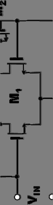
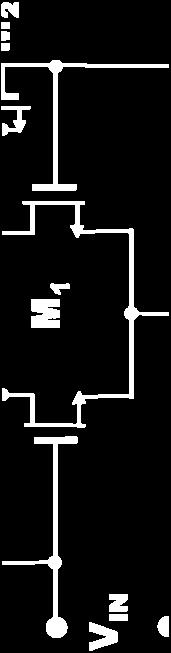
6 g m -Boosted Cascode meff [ 1 ( )] g = + A s g m Increases output resistance Reduces time constant at V x Ameliorates Miller effect at the input A 19-GHz Broadband Amplifier Using a g m -Boosted Cascode in 0.18-μm CMOS 6
7 g m -Boosted Cascode Passive g m - boosting: meff [ 1 ( )] g = + As g g = g for s = 0 meff m g = 2 g for s = meff m m A 19-GHz Broadband Amplifier Using a g m -Boosted Cascode in 0.18-μm CMOS 7
8 g m -Boosted Cascode L 1 separates C PAD and C IN [Sackinger 05] A 19-GHz Broadband Amplifier Using a g m -Boosted Cascode in 0.18-μm CMOS 8
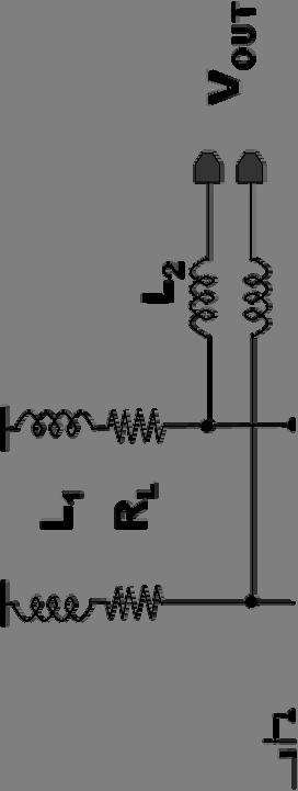
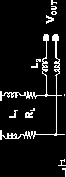
9 g m -Boosted Cascode L 2 separates the C D of M 1 and C S of M 2 [Analui 04] A 19-GHz Broadband Amplifier Using a g m -Boosted Cascode in 0.18-μm CMOS 9
10 g m -Boosted Cascode L3 and L4 provide series and shunt peaking [Lee 04] A 19-GHz Broadband Amplifier Using a g m -Boosted Cascode in 0.18-μm CMOS 10
11 g m -Boosted Cascode 3-dB Bandwidth (GHz) > 30 % improvement C (ff) R = 500Ω A 19-GHz Broadband Amplifier Using a g m -Boosted Cascode in 0.18-μm CMOS 11


12 Differential g m -Boosted Cascode R L is divided to improve the BW [Greshishchev 99] Feedback sets the input resistance to 50 Ω 1.2 ma 15 ma A 19-GHz Broadband Amplifier Using a g m -Boosted Cascode in 0.18-μm CMOS 12

13 Differential g m -Boosted Cascode 1.6 mm 0.7 mm Output Buffer A 19-GHz Broadband Amplifier Using a g m -Boosted Cascode in 0.18-μm CMOS 13


14 Measurement of g m -Boosted Pre-amp 2 port VNA 50 Ω DC Block DC Block 50 Ω A 19-GHz Broadband Amplifier Using a g m -Boosted Cascode in 0.18-μm CMOS 14
15 Measurement of g m -Boosted Pre-amp V DD = 2.5 V BW = 22 GHz 6 db was added to the S 21 measured on a 2-port network analyzer A 19-GHz Broadband Amplifier Using a g m -Boosted Cascode in 0.18-μm CMOS 15
16 Measurement of g m -Boosted Pre-amp V DD = 2.2 V BW = 21 GHz 6 db was added to the S 21 measured on a 2-port network analyzer A 19-GHz Broadband Amplifier Using a g m -Boosted Cascode in 0.18-μm CMOS 16

17 Measurement of g m -Boosted Pre-amp V DD = 2.5 V P 1dB for 6-GHz input A 19-GHz Broadband Amplifier Using a g m -Boosted Cascode in 0.18-μm CMOS 17

18 Measurement of g m -Boosted Pre-amp V DD = 2.5 V A 19-GHz Broadband Amplifier Using a g m -Boosted Cascode in 0.18-μm CMOS 18


19 Full Front End Design Bandwidth > 20 GHz Constant group delay Gain > 6 db 50-Ω Input Matching Bandwidth > 20 GHz Constant group delay Gain > 4 db 50-Ω output driver A 19-GHz Broadband Amplifier Using a g m -Boosted Cascode in 0.18-μm CMOS 19

20 Post-amplifier Used to cancel Miller capacitances A 19-GHz Broadband Amplifier Using a g m -Boosted Cascode in 0.18-μm CMOS 20
21 Post-amplifier L 1,L 2 chosen for maximally flat frequency response A 19-GHz Broadband Amplifier Using a g m -Boosted Cascode in 0.18-μm CMOS 21

22 Full Front End 2.0 mm 0.7 mm Cascode pre-amp 2 stage Post-amp G G S S G A 19-GHz Broadband Amplifier Using a g m -Boosted Cascode in 0.18-μm CMOS 22
23 Measurement of Full Front End V DD = 2.5 V BW = 19 GHz 6 db was added to the S 21 measured on a 2-port network analyzer A 19-GHz Broadband Amplifier Using a g m -Boosted Cascode in 0.18-μm CMOS 23
24 Measurement of Full Front End V DD = 2.2 V BW = 17.5 GHz 6 db was added to the S 21 measured on a 2-port network analyzer A 19-GHz Broadband Amplifier Using a g m -Boosted Cascode in 0.18-μm CMOS 24
25 Measurement of Full Front End V DD = 2.0 V BW = 16 GHz 6 db was added to the S 21 measured on a 2-port network analyzer A 19-GHz Broadband Amplifier Using a g m -Boosted Cascode in 0.18-μm CMOS 25


26 Measurement Setup for Eye Diagrams Agilent 86100C Scope Attenuator PRBS streams 4:1 Mux A 19-GHz Broadband Amplifier Using a g m -Boosted Cascode in 0.18-μm CMOS 26

27 Eye Diagram Measurements 20 Gb/s, 270 mvpp input amplitude A 19-GHz Broadband Amplifier Using a g m -Boosted Cascode in 0.18-μm CMOS 27
28 Eye Diagram Measurements 24 Gb/s, 270 mvpp input amplitude A 19-GHz Broadband Amplifier Using a g m -Boosted Cascode in 0.18-μm CMOS 28


29 Sensitivity Testing 14 Gb/s, 27 mvpp input amplitude 55 mv A 19-GHz Broadband Amplifier Using a g m -Boosted Cascode in 0.18-μm CMOS 29
30 Summary A 19-GHz Broadband Amplifier Using a g m -Boosted Cascode in 0.18-μm CMOS 30
31 Passive g m -boosting Conclusions Improves the time constant at cascode node Reduces Miller effect at the input node Does not reduce DC gain Does not introduce peaking No additional power consumption Pre-amplifier (only) achieves BW of 22 GHz in 0.18-µm CMOS Front end (pre-amp + post-amp) gain > 10 db is achieved with BW of 19 GHz A 19-GHz Broadband Amplifier Using a g m -Boosted Cascode in 0.18-μm CMOS 31
32 Acknowledgements Shahriar Shahramian Canadian Microelectronics Corporation Intel Corporation A 19-GHz Broadband Amplifier Using a g m -Boosted Cascode in 0.18-μm CMOS 32
33 Extras
34 Standard CMOS Cascode For example, assuming R in = 50 Ω, R L = 150 Ω, M1 & M2 are 20 x 2 μm, I D = 7.5 ma, C PAD = 70 ff, and C L = 40 ff: τ = 15pS out τ = 12pS cascode τ = input 9pS A 19-GHz Broadband Amplifier Using a g m -Boosted Cascode in 0.18-μm CMOS 34


35 Time Constants of g m -boosted Cascode A 19-GHz Broadband Amplifier Using a g m -Boosted Cascode in 0.18-μm CMOS 35

36 Differential g m -boosted Cascode G S G S G g m boosting : Improves Input time constant Improves the time cascode node Do not reduce DC Gain No additional DC power consumption G S G S G A 19-GHz Broadband Amplifier Using a g m -Boosted Cascode in 0.18-μm CMOS 36


37 Post Amplifier Implementation Post Amplifier G G S S G G G S S G A 19-GHz Broadband Amplifier Using a g m -Boosted Cascode in 0.18-μm CMOS 37
A 30-GS/sec Track and Hold Amplifier in 0.13-µm CMOS Technology Shahriar Shahramian Sorin P. Voinigescu Anthony Chan Carusone
 A 30-GS/sec Track and Hold Amplifier in 0.13-µm CMOS Technology Shahriar Shahramian Sorin P. Voinigescu Anthony Chan Carusone Department of Electrical & Computer Eng. University of Toronto Canada Introduction
6.776 High Speed Communication Circuits Lecture 7 High Freqeuncy, Broadband Amplifiers
 6.776 High Speed Communication Circuits Lecture 7 High Freqeuncy, Broadband Amplifiers Massachusetts Institute of Technology February 24, 2005 Copyright 2005 by Hae-Seung Lee and Michael H. Perrott High
ISSCC 2003 / SESSION 10 / HIGH SPEED BUILDING BLOCKS / PAPER 10.8
 ISSCC 2003 / SESSION 10 / HIGH SPEED BUILDING BLOCKS / PAPER 10.8 10.8 10Gb/s Limiting Amplifier and Laser/Modulator Driver in 0.18µm CMOS Technology Sherif Galal, Behzad Razavi Electrical Engineering
20 GHz Low Power QVCO and De-skew Techniques in 0.13µm Digital CMOS. Masum Hossain & Tony Chan Carusone University of Toronto
 20 GHz Low Power QVCO and De-skew Techniques in 0.13µm Digital CMOS Masum Hossain & Tony Chan Carusone University of Toronto masum@eecg.utoronto.ca Motivation Data Rx3 Rx2 D-FF D-FF Rx1 D-FF Clock Clock
Design Methodology and Applications of SiGe BiCMOS Cascode Opamps with up to 37-GHz Unity Gain Bandwidth
 Design Methodology and Applications of SiGe BiCMOS Cascode Opamps with up to 37-GHz Unity Gain Bandwidth S.P. Voinigescu, R. Beerkens*, T.O. Dickson, and T. Chalvatzis University of Toronto *STMicroelectronics,
95GHz Receiver with Fundamental Frequency VCO and Static Frequency Divider in 65nm Digital CMOS
 95GHz Receiver with Fundamental Frequency VCO and Static Frequency Divider in 65nm Digital CMOS Ekaterina Laskin, Mehdi Khanpour, Ricardo Aroca, Keith W. Tang, Patrice Garcia 1, Sorin P. Voinigescu University
CHAPTER 4 ULTRA WIDE BAND LOW NOISE AMPLIFIER DESIGN
 93 CHAPTER 4 ULTRA WIDE BAND LOW NOISE AMPLIFIER DESIGN 4.1 INTRODUCTION Ultra Wide Band (UWB) system is capable of transmitting data over a wide spectrum of frequency bands with low power and high data
ECEN689: Special Topics in High-Speed Links Circuits and Systems Spring 2012
 ECEN689: Special Topics in High-Speed Links Circuits and Systems Spring 2012 Lecture 5: Termination, TX Driver, & Multiplexer Circuits Sam Palermo Analog & Mixed-Signal Center Texas A&M University Announcements
SP 22.3: A 12mW Wide Dynamic Range CMOS Front-End for a Portable GPS Receiver
 SP 22.3: A 12mW Wide Dynamic Range CMOS Front-End for a Portable GPS Receiver Arvin R. Shahani, Derek K. Shaeffer, Thomas H. Lee Stanford University, Stanford, CA At submicron channel lengths, CMOS is
Lecture 25 - Frequency Response of Amplifiers (III) Other Amplifier Stages. December 8, 2005
 Other Amplifier Stages. December 8, 2005") 6.012 Microelectronic Devices and Circuits Fall 2005 Lecture 251 Lecture 25 Frequency Response of Amplifiers (III) Other Amplifier Stages December 8, 2005 Contents: 1. Frequency response of commondrain
6.012 Microelectronic Devices and Circuits Fall 2005 Lecture 251 Lecture 25 Frequency Response of Amplifiers (III) Other Amplifier Stages December 8, 2005 Contents: 1. Frequency response of commondrain
Lecture 20: Passive Mixers
 EECS 142 Lecture 20: Passive Mixers Prof. Ali M. Niknejad University of California, Berkeley Copyright c 2005 by Ali M. Niknejad A. M. Niknejad University of California, Berkeley EECS 142 Lecture 20 p.
A Low Power Integrated UWB Transceiver with Solar Energy Harvesting for Wireless Image Sensor Networks
 A Low Power Integrated UWB Transceiver with Solar Energy Harvesting for Wireless Image Sensor Networks Minjoo Yoo / Jaehyuk Choi / Ming hao Wang April. 13 th. 2009 Contents Introduction Circuit Description
The GBTIA, a 5 Gbit/s Radiation-Hard Optical Receiver for the SLHC Upgrades
 The GBTIA, a 5 Gbit/s Radiation-Hard Optical Receiver for the SLHC Upgrades M. Menouni a, P. Gui b, P. Moreira c a CPPM, Université de la méditerranée, CNRS/IN2P3, Marseille, France b SMU, Southern Methodist
EE105 Fall 2015 Microelectronic Devices and Circuits
 EE105 Fall 2015 Microelectronic Devices and Circuits Multi-Stage Amplifiers Prof. Ming C. Wu wu@eecs.berkeley.edu 511 Sutardja Dai Hall (SDH) Terminal Gain and I/O Resistances of MOS Amplifiers Common
Measurement and Modeling of CMOS Devices in Short Millimeter Wave. Minoru Fujishima
 Measurement and Modeling of CMOS Devices in Short Millimeter Wave Minoru Fujishima Our position We are circuit designers. Our final target is not device modeling, but chip demonstration. Provided device
HIGH-GAIN CMOS LOW NOISE AMPLIFIER FOR ULTRA WIDE-BAND WIRELESS RECEIVER
 Progress In Electromagnetics Research C, Vol. 7, 183 191, 2009 HIGH-GAIN CMOS LOW NOISE AMPLIFIER FOR ULTRA WIDE-BAND WIRELESS RECEIVER A. Dorafshan and M. Soleimani Electrical Engineering Department Iran
Low-Noise Amplifiers
 007/Oct 4, 31 1 General Considerations Noise Figure Low-Noise Amplifiers Table 6.1 Typical LNA characteristics in heterodyne systems. NF IIP 3 db 10 dbm Gain 15 db Input and Output Impedance 50 Ω Input
Preliminary Exam, Fall 2013 Department of Electrical and Computer Engineering University of California, Irvine EECS 170B
 Preliminary Exam, Fall 2013 Department of Electrical and Computer Engineering University of California, Irvine EECS 170B Problem 1. Consider the following circuit, where a saw-tooth voltage is applied
ECEN 720 High-Speed Links: Circuits and Systems. Lab3 Transmitter Circuits. Objective. Introduction. Transmitter Automatic Termination Adjustment
 1 ECEN 720 High-Speed Links: Circuits and Systems Lab3 Transmitter Circuits Objective To learn fundamentals of transmitter and receiver circuits. Introduction Transmitters are used to pass data stream
Lecture 33: Context. Prof. J. S. Smith
 Lecture 33: Prof J. S. Smith Context We are continuing to review some of the building blocks for multi-stage amplifiers, including current sources and cascode connected devices, and we will also look at
Nonlinear Macromodeling of Amplifiers and Applications to Filter Design.
 ECEN 622 Nonlinear Macromodeling of Amplifiers and Applications to Filter Design. By Edgar Sanchez-Sinencio Thanks to Heng Zhang for part of the material OP AMP MACROMODELS Systems containing a significant
Document Version Publisher s PDF, also known as Version of Record (includes final page, issue and volume numbers)
") A 40 GHz, broadband, highly linear amplifier, employing T-coil bandwith extension technique Cheema, H.M.; Mahmoudi, R.; Sanduleanu, M.A.T.; van Roermund, A.H.M. Published in: IEEE Radio Frequency Integrated
A 40 GHz, broadband, highly linear amplifier, employing T-coil bandwith extension technique Cheema, H.M.; Mahmoudi, R.; Sanduleanu, M.A.T.; van Roermund, A.H.M. Published in: IEEE Radio Frequency Integrated
Design and Simulation Study of Active Balun Circuits for WiMAX Applications
 Design and Simulation Study of Circuits for WiMAX Applications Frederick Ray I. Gomez 1,2,*, John Richard E. Hizon 2 and Maria Theresa G. De Leon 2 1 New Product Introduction Department, Back-End Manufacturing
International Journal of Pure and Applied Mathematics
 Volume 118 No. 0 018, 4187-4194 ISSN: 1314-3395 (on-line version) url: http://www.ijpam.eu ijpam.eu A 5- GHz CMOS Low Noise Amplifier with High gain and Low power using Pre-distortion technique A.Vidhya
A 2.4GHz Fully Integrated CMOS Power Amplifier Using Capacitive Cross-Coupling
 A 2.4GHz Fully Integrated CMOS Power Amplifier Using Capacitive Cross-Coupling JeeYoung Hong, Daisuke Imanishi, Kenichi Okada, and Akira Tokyo Institute of Technology, Japan Contents 1 Introduction PA
ECEN 720 High-Speed Links: Circuits and Systems
 1 ECEN 720 High-Speed Links: Circuits and Systems Lab4 Receiver Circuits Objective To learn fundamentals of receiver circuits. Introduction Receivers are used to recover the data stream transmitted by
Design for MOSIS Educational Program (Research) Testing Report for Project Number 89742
 Testing Report for Project Number 89742") Design for MOSIS Educational Program (Research) Testing Report for Project Number 89742 Prepared By: Kossi Sessou (Graduate Student) and Nathan Neihart (Assistant Professor) Bin Huang (Graduate Student)
Design for MOSIS Educational Program (Research) Testing Report for Project Number 89742 Prepared By: Kossi Sessou (Graduate Student) and Nathan Neihart (Assistant Professor) Bin Huang (Graduate Student)
A 2.4 GHZ RECEIVER IN SILICON-ON-SAPPHIRE MICHAEL PETERS. B.S., Kansas State University, 2009 A REPORT
 A 2.4 GHZ RECEIVER IN SILICON-ON-SAPPHIRE by MICHAEL PETERS B.S., Kansas State University, 2009 A REPORT submitted in partial fulfillment of the requirements for the degree MASTER OF SCIENCE Department
O.13f-Lm 1.OV-l.5V Supply Digital Blocks for 40-Gb/s Optical Communication Systems
 O.13f-Lm 1.OV-l.5V Supply Digital Blocks for 40-Gb/s Optical Communication Systems Bangli Liang, Tad Kwasniewski Department of Electronics Carleton University Ottawa, Ontario, Canada Email: bliang.tak@doe.carleton.ca
Nonlinear Macromodeling of Amplifiers and Applications to Filter Design.
 ECEN 622(ESS) Nonlinear Macromodeling of Amplifiers and Applications to Filter Design. By Edgar Sanchez-Sinencio Thanks to Heng Zhang for part of the material OP AMP MACROMODELS Systems containing a significant
A 5-Gb/s 156-mW Transceiver with FFE/Analog Equalizer in 90-nm CMOS Technology Wang Xinghua a, Wang Zhengchen b, Gui Xiaoyan c,
 4th International Conference on Computer, Mechatronics, Control and Electronic Engineering (ICCMCEE 2015) A 5-Gb/s 156-mW Transceiver with FFE/Analog Equalizer in 90-nm CMOS Technology Wang Xinghua a,
Reading. Lecture 33: Context. Lecture Outline. Chapter 9, multi-stage amplifiers. Prof. J. S. Smith
 eading Lecture 33: Chapter 9, multi-stage amplifiers Prof J. S. Smith Context Lecture Outline We are continuing to review some of the building blocks for multi-stage amplifiers, including current sources
You will be asked to make the following statement and provide your signature on the top of your solutions.
 1 EE 435 Name Exam 1 Spring 216 Instructions: The points allocated to each problem are as indicated. Note that the first and last problem are weighted more heavily than the rest of the problems. On those
ECEN 720 High-Speed Links Circuits and Systems
 1 ECEN 720 High-Speed Links Circuits and Systems Lab4 Receiver Circuits Objective To learn fundamentals of receiver circuits. Introduction Receivers are used to recover the data stream transmitted by transmitters.
A GSM Band Low-Power LNA 1. LNA Schematic
 A GSM Band Low-Power LNA 1. LNA Schematic Fig1.1 Schematic of the Designed LNA 2. Design Summary Specification Required Simulation Results Peak S21 (Gain) > 10dB >11 db 3dB Bandwidth > 200MHz (
TWO AND ONE STAGES OTA
 TWO AND ONE STAGES OTA F. Maloberti Department of Electronics Integrated Microsystem Group University of Pavia, 7100 Pavia, Italy franco@ele.unipv.it tel. +39-38-50505; fax. +39-038-505677 474 EE Department
ISSCC 2004 / SESSION 26 / OPTICAL AND FAST I/O / 26.6
 ISSCC 2004 / SESSION 26 / OPTICAL AND FAST I/O / 26.6 26.6 40Gb/s Amplifier and ESD Protection Circuit in 0.18µm CMOS Technology Sherif Galal, Behzad Razavi University of California, Los Angeles, CA Optical
A Three-Stage 60GHz CMOS LNA Using Dual Noise-Matching Technique for 5dB NF
 A Three-Stage 60GHz CMOS LNA Using Dual Noise-Matching Technique for 5dB NF Ning Li 1, Kenichi Okada 1, Toshihide Suzuki 2, Tatsuya Hirose 2 and Akira 1 1. Tokyo Institute of Technology, Japan 2. Advanced
Radivoje Đurić, 2015, Analogna Integrisana Kola 1
 Low power OTA 1 Two-Stage, Miller Op Amp Operating in Weak Inversion Low frequency response: gm1 gm6 Av 0 g g g g A v 0 ds2 ds4 ds6 ds7 I D m, ds D nvt g g I n GB and SR: GB 1 1 n 1 2 4 6 6 7 g 2 2 m1
56 Gb/s 4:1 Multiplexer Module
 MS4S1V2M Datasheet CENTELLAX Description Applications The MS4S1V2M can be used with existing equipment to generate higher rate bit streams for use in telecom applications up to 56 Gb/s. Broadband test
CHAPTER 3 CMOS LOW NOISE AMPLIFIERS
 46 CHAPTER 3 CMOS LOW NOISE AMPLIFIERS 3.1 INTRODUCTION The Low Noise Amplifier (LNA) plays an important role in the receiver design. LNA serves as the first block in the RF receiver. It is a critical
ISSCC 2004 / SESSION 26 / OPTICAL AND FAST I/O / 26.8
 ISSCC 2004 / SESSION 26 / OPTICAL AND FAST I/O / 26.8 26.8 A 2GHz CMOS Variable-Gain Amplifier with 50dB Linear-in-Magnitude Controlled Gain Range for 10GBase-LX4 Ethernet Chia-Hsin Wu, Chang-Shun Liu,
Rail-To-Rail Output Op-Amp Design with Negative Miller Capacitance Compensation
 Rail-To-Rail Op-Amp Design with Negative Miller Capacitance Compensation Muhaned Zaidi, Ian Grout, Abu Khari bin A ain Abstract In this paper, a two-stage op-amp design is considered using both Miller
A 2.4GHz Cascode CMOS Low Noise Amplifier
 A 2.4GHz Cascode CMOS Low Noise Amplifier Gustavo Campos Martins, Fernando Rangel de Sousa Federal University of Santa Catarina (UFSC) Integrated Circuits Laboratory (LCI) August 31, 2012 G. C. Martins,
6.976 High Speed Communication Circuits and Systems Lecture 5 High Speed, Broadband Amplifiers
 6.976 High Speed Communication Circuits and Systems Lecture 5 High Speed, Broadband Amplifiers Michael Perrott Massachusetts Institute of Technology Copyright 2003 by Michael H. Perrott Broadband Communication
Design technique of broadband CMOS LNA for DC 11 GHz SDR
 Design technique of broadband CMOS LNA for DC 11 GHz SDR Anh Tuan Phan a) and Ronan Farrell Institute of Microelectronics and Wireless Systems, National University of Ireland Maynooth, Maynooth,Co. Kildare,
Design and Simulation of Low Voltage Operational Amplifier
 Design and Simulation of Low Voltage Operational Amplifier Zach Nelson Department of Electrical Engineering, University of Nevada, Las Vegas 4505 S Maryland Pkwy, Las Vegas, NV 89154 United States of America
Analysis and Design of Analog Integrated Circuits Lecture 20. Advanced Opamp Topologies (Part II)
") Analysis and Design of Analog Integrated Circuits Lecture 20 Advanced Opamp Topologies (Part II) Michael H. Perrott April 15, 2012 Copyright 2012 by Michael H. Perrott All rights reserved. Outline of Lecture
Analysis and Design of Analog Integrated Circuits Lecture 20 Advanced Opamp Topologies (Part II) Michael H. Perrott April 15, 2012 Copyright 2012 by Michael H. Perrott All rights reserved. Outline of Lecture
Performance Evaluation of Different Types of CMOS Operational Transconductance Amplifier
 Performance Evaluation of Different Types of CMOS Operational Transconductance Amplifier Kalpesh B. Pandya 1, Kehul A. shah 2 1 Gujarat Technological University, Department of Electronics & Communication,
Lecture 2: Non-Ideal Amps and Op-Amps
 Lecture 2: Non-Ideal Amps and Op-Amps Prof. Ali M. Niknejad Department of EECS University of California, Berkeley Practical Op-Amps Linear Imperfections: Finite open-loop gain (A 0 < ) Finite input resistance
CMOS LNA Design for Ultra Wide Band - Review
 International Journal of Innovation and Scientific Research ISSN 235-804 Vol. No. 2 Nov. 204, pp. 356-362 204 Innovative Space of Scientific Research Journals http://www.ijisr.issr-journals.org/ CMOS LNA
You will be asked to make the following statement and provide your signature on the top of your solutions.
 1 EE 435 Name Exam 1 Spring 2018 Instructions: The points allocated to each problem are as indicated. Note that the first and last problem are weighted more heavily than the rest of the problems. On those
** Dice/wafers are designed to operate from -40 C to +85 C, but +3.3V. V CC LIMITING AMPLIFIER C FILTER 470pF PHOTODIODE FILTER OUT+ IN TIA OUT-
 19-2105; Rev 2; 7/06 +3.3V, 2.5Gbps Low-Power General Description The transimpedance amplifier provides a compact low-power solution for 2.5Gbps communications. It features 495nA input-referred noise,
Low-Power RF Integrated Circuit Design Techniques for Short-Range Wireless Connectivity
 Low-Power RF Integrated Circuit Design Techniques for Short-Range Wireless Connectivity Marvin Onabajo Assistant Professor Analog and Mixed-Signal Integrated Circuits (AMSIC) Research Laboratory Dept.
Electronic Dispersion Compensation of 40-Gb/s Multimode Fiber Links Using IIR Equalization
 Electronic Dispersion Compensation of 4-Gb/s Multimode Fiber Links Using IIR Equalization George Ng & Anthony Chan Carusone Dept. of Electrical & Computer Engineering University of Toronto Canada Transmitting
Lecture 21: Voltage/Current Buffer Freq Response
 Lecture 21: Voltage/Current Buffer Freq Response Prof. Niknejad Lecture Outline Last Time: Frequency Response of Voltage Buffer Frequency Response of Current Buffer Current Mirrors Biasing Schemes Detailed
Basic Circuits. Current Mirror, Gain stage, Source Follower, Cascode, Differential Pair,
 Basic Circuits Current Mirror, Gain stage, Source Follower, Cascode, Differential Pair, CCS - Basic Circuits P. Fischer, ZITI, Uni Heidelberg, Seite 1 Reminder: Effect of Transistor Sizes Very crude classification:
A 25MS/s 14b 200mW Σ Modulator in 0.18µm CMOS
 UT Mixed-Signal/RF Integrated Circuits Seminar Series A 25MS/s 14b 200mW Σ Modulator in 0.18µm CMOS Pio Balmelli April 19 th, Austin TX 2 Outline VDSL specifications Σ A/D converter features Broadband
Multi-Gb/s Bit-by-Bit Receiver Architectures for 1 D Partial Response Channels
 SUBMITTED: IEEE TRANSACTION ON CIRCUITS AND SYSTEMS-I, VOL., NO., SEPTEMBER 2008 1 Multi-Gb/s Bit-by-Bit Receiver Architectures for 1 D Partial Response Channels Masum Hossain, Anthony Chan Carusone, Senior
6.776 High Speed Communication Circuits Lecture 6 MOS Transistors, Passive Components, Gain- Bandwidth Issue for Broadband Amplifiers
 6.776 High Speed Communication Circuits Lecture 6 MOS Transistors, Passive Components, Gain- Bandwidth Issue for Broadband Amplifiers Massachusetts Institute of Technology February 17, 2005 Copyright 2005
A new class AB folded-cascode operational amplifier
 A new class AB folded-cascode operational amplifier Mohammad Yavari a) Integrated Circuits Design Laboratory, Department of Electrical Engineering, Amirkabir University of Technology, Tehran, Iran a) myavari@aut.ac.ir
1-13GHz Wideband LNA utilizing a Transformer as a Compact Inter-stage Network in 65nm CMOS
 -3GHz Wideband LNA utilizing a Transformer as a Compact Inter-stage Network in 65nm CMOS Hyohyun Nam and Jung-Dong Park a Division of Electronics and Electrical Engineering, Dongguk University, Seoul E-mail
Probing for oscilloscope
 Probing for oscilloscope Agenda - Notion de sonde en oscilloscopie - Structure des différentes sondes - Passives - Actives - Logiques - Différentielles - Comment choisir la bonne sonde - Nouvelle technologie
65-GHz Receiver in SiGe BiCMOS Using Monolithic Inductors and Transformers
 65-GHz Receiver in SiGe BiCMOS Using Monolithic Inductors and Transformers Michael Gordon, Terry Yao, Sorin P. Voinigescu University of Toronto March 10 2006, UBC, Vancouver Outline Motivation mm-wave
A 16Ω Audio Amplifier with 93.8 mw Peak loadpower and 1.43 quiscent power consumption
 A 16Ω Audio Amplifier with 93.8 mw Peak loadpower and 1.43 quiscent power consumption IEEE Transactions on circuits and systems- Vol 59 No:3 March 2012 Abstract A class AB audio amplifier is used to drive
An Analog Phase-Locked Loop
 1 An Analog Phase-Locked Loop Greg Flewelling ABSTRACT This report discusses the design, simulation, and layout of an Analog Phase-Locked Loop (APLL). The circuit consists of five major parts: A differential
AVoltage Controlled Oscillator (VCO) was designed and
 was designed and") 1 EECE 457 VCO Design Project Jason Khuu, Erik Wu Abstract This paper details the design and simulation of a Voltage Controlled Oscillator using a 0.13µm process. The final VCO design meets all specifications.
1 EECE 457 VCO Design Project Jason Khuu, Erik Wu Abstract This paper details the design and simulation of a Voltage Controlled Oscillator using a 0.13µm process. The final VCO design meets all specifications.
Operational Amplifiers
 CHAPTER 9 Operational Amplifiers Analog IC Analysis and Design 9- Chih-Cheng Hsieh Outline. General Consideration. One-Stage Op Amps / Two-Stage Op Amps 3. Gain Boosting 4. Common-Mode Feedback 5. Input
On Chip Active Decoupling Capacitors for Supply Noise Reduction for Power Gating and Dynamic Dual Vdd Circuits in Digital VLSI
 ELEN 689 606 Techniques for Layout Synthesis and Simulation in EDA Project Report On Chip Active Decoupling Capacitors for Supply Noise Reduction for Power Gating and Dynamic Dual Vdd Circuits in Digital
High Voltage Operational Amplifiers in SOI Technology
 High Voltage Operational Amplifiers in SOI Technology Kishore Penmetsa, Kenneth V. Noren, Herbert L. Hess and Kevin M. Buck Department of Electrical Engineering, University of Idaho Abstract This paper
Hot Topics and Cool Ideas in Scaled CMOS Analog Design
 Engineering Insights 2006 Hot Topics and Cool Ideas in Scaled CMOS Analog Design C. Patrick Yue ECE, UCSB October 27, 2006 Slide 1 Our Research Focus High-speed analog and RF circuits Device modeling,
Chapter 12 Opertational Amplifier Circuits
 1 Chapter 12 Opertational Amplifier Circuits Learning Objectives 1) The design and analysis of the two basic CMOS op-amp architectures: the two-stage circuit and the single-stage, folded cascode circuit.
5Gbps Serial Link Transmitter with Pre-emphasis
 Gbps Serial Link Transmitter with Pre-emphasis Chih-Hsien Lin, Chung-Hong Wang and Shyh-Jye Jou Department of Electrical Engineering,National Central University,Chung-Li, Taiwan R.O.C. Abstract- High-speed
Low-power 2.5 Gbps VCSEL driver in 0.5 µm CMOS technology
 Low-power 2.5 Gbps VCSEL driver in 0.5 µm CMOS technology Bindu Madhavan and A. F. J. Levi Department of Electrical Engineering University of Southern California Los Angeles, California 90089-1111 Indexing
Designing of Low Power RF-Receiver Front-end with CMOS Technology
 Sareh Salari Shahrbabaki Designing of Low Power RF-Receiver Front-end with CMOS Technology School of Electrical Engineering Thesis submitted for examination for the degree of Master of Science in Technology.
Inductorless CMOS Receiver Front-End Circuits for 10-Gb/s Optical Communications
 Tamkang Journal of Science and Engineering, Vol. 12, No. 4, pp. 449 458 (2009) 449 Inductorless CMOS Receiver Front-End Circuits for 10-Gb/s Optical Communications Hsin-Liang Chen*, Chih-Hao Chen, Wei-Bin
Massachusetts Institute of Technology Department of Electrical Engineering and Computer Science
 Massachusetts Institute of Technology Department of Electrical Engineering and Computer Science 6.976 High Speed Communication Circuits and Systems Spring 2003 Homework #4: Narrowband LNA s and Mixers
An 8-Gb/s Inductorless Adaptive Passive Equalizer in µm CMOS Technology
 JOURNAL OF SEMICONDUCTOR TECHNOLOGY AND SCIENCE, VOL.12, NO.4, DECEMBER, 2012 http://dx.doi.org/10.5573/jsts.2012.12.4.405 An 8-Gb/s Inductorless Adaptive Passive Equalizer in 0.18- µm CMOS Technology
10.1: A 4 GSample/s 8b ADC in 0.35-um CMOS
 10.1: A 4 GSample/s 8b ADC in 0.35-um CMOS Ken Poulton, Robert Neff, Art Muto, Wei Liu*, Andy Burstein**, Mehrdad Heshami*** Agilent Technologies, Palo Alto, CA *Agilent Technologies, Colorado Springs,
ECE 415/515 ANALOG INTEGRATED CIRCUIT DESIGN
 ECE 415/515 ANALOG INTEGRATED CIRCUIT DESIGN OPAMP DESIGN AND SIMULATION Vishal Saxena OPAMP DESIGN PROJECT R 2 v out v in /2 R 1 C L v in v out V CM R L V CM C L V CM -v in /2 R 1 C L (a) (b) R 2 ECE415/EO
PROJECT ON MIXED SIGNAL VLSI
 PROJECT ON MXED SGNAL VLS Submitted by Vipul Patel TOPC: A GLBERT CELL MXER N CMOS AND BJT TECHNOLOGY 1 A Gilbert Cell Mixer in CMOS and BJT technology Vipul Patel Abstract This paper describes a doubly
Design of low-loss 60 GHz integrated antenna switch in 65 nm CMOS
 LETTER IEICE Electronics Express, Vol.15, No.7, 1 10 Design of low-loss 60 GHz integrated antenna switch in 65 nm CMOS Korkut Kaan Tokgoz a), Seitaro Kawai, Kenichi Okada, and Akira Matsuzawa Department
DESIGN OF 3 TO 5 GHz CMOS LOW NOISE AMPLIFIER FOR ULTRA-WIDEBAND (UWB) SYSTEM
 SYSTEM") Progress In Electromagnetics Research C, Vol. 9, 25 34, 2009 DESIGN OF 3 TO 5 GHz CMOS LOW NOISE AMPLIFIER FOR ULTRA-WIDEBAND (UWB) SYSTEM S.-K. Wong and F. Kung Faculty of Engineering Multimedia University
Progress In Electromagnetics Research C, Vol. 9, 25 34, 2009 DESIGN OF 3 TO 5 GHz CMOS LOW NOISE AMPLIFIER FOR ULTRA-WIDEBAND (UWB) SYSTEM S.-K. Wong and F. Kung Faculty of Engineering Multimedia University
A 60GHz CMOS Power Amplifier Using Varactor Cross-Coupling Neutralization with Adaptive Bias
 A 6GHz CMOS Power Amplifier Using Varactor Cross-Coupling Neutralization with Adaptive Bias Ryo Minami,Kota Matsushita, Hiroki Asada, Kenichi Okada,and Akira Tokyo Institute of Technology, Japan Outline
Comparative Analysis of Compensation Techniques for improving PSRR of an OPAMP
 Comparative Analysis of Compensation Techniques for improving PSRR of an OPAMP 1 Pathak Jay, 2 Sanjay Kumar M.Tech VLSI and Embedded System Design, Department of School of Electronics, KIIT University,
A12 10 Gb/s fully integrated CMOS parallel optical receiver front-end amplifier array
 . RESEARCH PAPER. SCIENCE CHINA Information Sciences June 2012 Vol. 55 No. 6: 1415 1428 doi: 10.1007/s11432-011-4385-6 A12 10 Gb/s fully integrated CMOS parallel optical receiver front-end amplifier array
DC Coupling: General Trends
 DC Coupling: General Trends * Goal: want both input and output to be centered at halfway between the positive and negative supplies (or ground, for a single supply) -- in order to have maximum possible
Low-Power Pipelined ADC Design for Wireless LANs
 Low-Power Pipelined ADC Design for Wireless LANs J. Arias, D. Bisbal, J. San Pablo, L. Quintanilla, L. Enriquez, J. Vicente, J. Barbolla Dept. de Electricidad y Electrónica, E.T.S.I. de Telecomunicación,
High-Speed Data Communication LA310Z 8.3 GHz Differential Limiting Amplifier 16-pin Plastic QFN Package
 High-Speed Data Communication LA10Z 8. GHz Differential Limiting Amplifier 16-pin Plastic QFN Package PRODUCT DESCRIPTION The LA10Z is an ultra-broadband fully differential limiting amplifier designed
ISSCC 2004 / SESSION 26 / OPTICAL AND FAST I/O / 26.4
 ISSCC 2004 / SESSION 26 / OPTICAL AND FAST I/O / 26.4 26.4 40Gb/s CMOS Distributed Amplifier for Fiber-Optic Communication Systems H. Shigematsu 1, M. Sato 1, T. Hirose 1, F. Brewer 2, M. Rodwell 2 1 Fujitsu,
AN-1106 Custom Instrumentation Amplifier Design Author: Craig Cary Date: January 16, 2017
 AN-1106 Custom Instrumentation Author: Craig Cary Date: January 16, 2017 Abstract This application note describes some of the fine points of designing an instrumentation amplifier with op-amps. We will
ETIN25 Analogue IC Design. Laboratory Manual Lab 2
 Department of Electrical and Information Technology LTH ETIN25 Analogue IC Design Laboratory Manual Lab 2 Jonas Lindstrand Martin Liliebladh Markus Törmänen September 2011 Laboratory 2: Design and Simulation
Designing a fully integrated low noise Tunable-Q Active Inductor for RF applications
 Designing a fully integrated low noise Tunable-Q Active Inductor for RF applications M. Ikram Malek, Suman Saini National Institute of technology, Kurukshetra Kurukshetra, India Abstract Many architectures
A10-Gb/slow-power adaptive continuous-time linear equalizer using asynchronous under-sampling histogram
 LETTER IEICE Electronics Express, Vol.10, No.4, 1 8 A10-Gb/slow-power adaptive continuous-time linear equalizer using asynchronous under-sampling histogram Wang-Soo Kim and Woo-Young Choi a) Department
C H A P T E R 5. Amplifier Design
 C H A P T E 5 Amplifier Design The Common-Source Amplifier v 0 = r ( g mvgs )( D 0 ) A v0 = g m r ( D 0 ) Performing the analysis directly on the circuit diagram with the MOSFET model used implicitly.
Chapter 2 CMOS at Millimeter Wave Frequencies
 Chapter 2 CMOS at Millimeter Wave Frequencies In the past, mm-wave integrated circuits were always designed in high-performance RF technologies due to the limited performance of the standard CMOS transistors
A COMPACT WIDEBAND MATCHING 0.18-µM CMOS UWB LOW-NOISE AMPLIFIER USING ACTIVE FEED- BACK TECHNIQUE
 Progress In Electromagnetics Research C, Vol. 16, 161 169, 2010 A COMPACT WIDEBAND MATCHING 0.18-µM CMOS UWB LOW-NOISE AMPLIFIER USING ACTIVE FEED- BACK TECHNIQUE J.-Y. Li, W.-J. Lin, and M.-P. Houng Department
A Broadband Transimpedance Amplifier with Optimum Bias Network Qian Gao 1, a, Sheng Xie 1, b*, Luhong Mao 1, c and Sicong Wu 1, d
 6th International Conference on Management, Education, Information and Control (MEICI 06) A Broadband Transimpedance Amplifier with Optimum Bias etwork Qian Gao, a, Sheng Xie, b*, Luhong Mao, c and Sicong
ISSCC 2004 / SESSION 25 / HIGH-RESOLUTION NYQUIST ADCs / 25.4
 ISSCC 2004 / SESSION 25 / HIGH-RESOLUTION NYQUIST ADCs / 25.4 25.4 A 1.8V 14b 10MS/s Pipelined ADC in 0.18µm CMOS with 99dB SFDR Yun Chiu, Paul R. Gray, Borivoje Nikolic University of California, Berkeley,
Preamplifier shaper: The preamplifier. The shaper. The Output.
 Preamplifier shaper: In previous simulations I just tried to reach the speed limits. The only way to realise this was by using a lot of current, about 1 ma through the input transistor. This gives in the