Chapter 4 O t p ica c l a So S u o r u ce c s
|
|
|
- Beatrice Fay Day
- 6 years ago
- Views:
Transcription
1 Chapter 4 Optical Sources
2 Contents Review of Semiconductor Physics Light Emitting Diode (LED) - Structure, Material,Quantum efficiency, LED Power, Modulation Laser Diodes - structure, Modes, Rate Equation,Quantum efficiency, Resonant frequencies, Radiation pattern Single-Mode Lasers - DFB (Distributed-FeedBack) laser, Distributed- Bragg Reflector, Modulation Light-source Linearity Noise in Lasers
3 Considerations with Optical Sources Physical dimensions to suit the fiber Narrow radiation pattern (beam width) Linearity (output light power proportional to driving current) Ability to be directly modulated by varying driving current Fast response time (wide band) Adequate output power into the fiber
4 Considerations Narrow spectral width (or line width) Stability and efficiency Driving circuit issues Reliability and cost
5 Semiconductor Light Sources A PN junction (that consists of direct band gap semiconductor materials) acts as the active or recombination region. When the PN junction is forward biased, electrons and holes recombine either radiatively (emitting photons) or non-radiatively (emitting heat). This is simple LED operation. In a LASER, the photon is further processed in a resonance cavity to achieve a coherent, highly directional optical beam with narrow linewidth.
6 LED vs. laser spectral width Single-frequency laser (<0.04 nm) Laser output is many times higher than LED output; they would not show on same scale Standard laser (1-3 nm wide) LED (30-50 nm wide) Wavelength
7 Review of Semiconductor Physics k B = JK -1 a) Energy level diagrams showing the excitation of an electron from the valence band to the conduction band. The resultant free electron can freely move under the application of electric field. b) Equal electron & hole concentrations in an intrinsic semiconductor created by the thermal excitation of electrons across the band gap Optical Fiber communications, 3 rd ed.,g.keiser,mcgrawhill, 2000
8 n-type Semiconductor a) Donor level in an n-type semiconductor. b) The ionization of donor impurities creates an increased electron concentration distribution. Optical Fiber communications, 3 rd ed.,g.keiser,mcgrawhill, 2000
9 p-type Semiconductor a) Acceptor level in an p-type semiconductor. b) The ionization of acceptor impurities creates an increased hole concentration distribution Optical Fiber communications, 3 rd ed.,g.keiser,mcgrawhill, 2000
10 Intrinsic & Extrinsic Materials Intrinsic material: A perfect material with no impurities. n & E g p & ni are the n = 2k Extrinsic material: donor or acceptor type semiconductors. p electron, = is the gap energy, T n i hole is exp( & intrinsic E g B T ) concentrat Temperature. ions [4-1] 2 pn = n i [4-2] respective Majority carriers: electrons in n-type or holes in p-type. Minority carriers: holes in n-type or electrons in p-type. The operation of semiconductor devices is essentially based on the injection and extraction of minority carriers. ly.
11 The pn Junction Electron diffusion across a pn junction creates a barrier potential (electric field) in the depletion region. Optical Fiber communications, 3 rd ed.,g.keiser,mcgrawhill, 2000
12 Reverse-biased pn Junction A reverse bias widens the depletion region, but allows minority carriers to move freely with the applied field. Optical Fiber communications, 3 rd ed.,g.keiser,mcgrawhill, 2000
13 Forward-biased pn Junction Lowering the barrier potential with a forward bias allows majority carriers to diffuse across the junction. Optical Fiber communications, 3 rd ed.,g.keiser,mcgrawhill, 2000
14 Direct Band Gap Semiconductors The E-k Diagram E k The Energy Band Diagram Conduction Band (CB) E g e - E c Empty ψ k hυ E c E v E v CB e - hυ Valence Band (VB) h + Occupied ψ h + k VB š /a The E-k diagram of a direct bandgap semiconductor such as GaAs. The E-k curve consists of many discrete points with each point corresponding to a possible state, wavefunction ψ k (x), that is allowed to exist in the crystal. The points are so close that we normally draw the E-k relationship as a continuous curve. In the energy range E v to E c there are no points (ψ k (x) solutions). š /a 1999 S.O. Kasap, Optoelectronics (Prentice Hall) k
15 Indirect Band Gap Semiconductors E E E Direct Bandgap E g CB E c E v Photon CB Indirect Bandgap, E g k cb E c E r CB E c Phonon k VB k k VB k vb E v k k VB E v k (a) GaAs (b) Si (c) Si with a recombination center (a) In GaAs the minimum of the CB is directly above the maximum of the VB. GaAs is therefore a direct bandgap semiconductor. (b) In Si, the minimum of the CB is displaced from the maximum of the VB and Si is an indirect bandgap semiconductor. (c) Recombination of an electron and a hole in Si involves a recombination center S.O. Kasap, Optoelectronics (Prentice Hall)

16 Periodic table
17 Light-Emitting Diodes (LEDs) For photonic communications requiring data rate Mb/s with multimode fiber with tens of microwatts, LEDs are usually the best choice. LED configurations being used in photonic communications: 1- Surface Emitters (Front Emitters) 2- Edge Emitters
18 Cross-section drawing of a typical GaAlAs double heterostructure light emitter. In this structure, x>y to provide for both carrier confinement and optical guiding. b) Energy-band diagram showing the active region, the electron & hole barriers which confine the charge carriers to the active layer. c) Variations in the refractive index; the lower refractive index of the material in regions 1 and 5 creates an optical barrier around the waveguide because of the higher band-gap energy of this material. λ( µ m) = (ev) E g Optical Fiber communications, 3 rd ed.,g.keiser,mcgrawhill, 2000
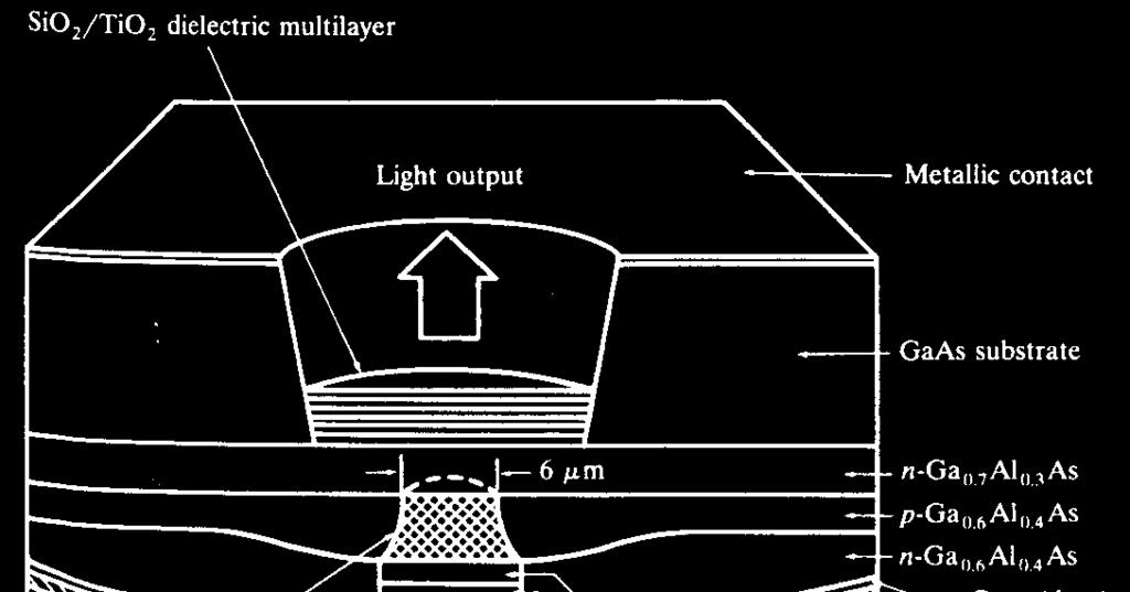
19 Surface-Emitting LED Schematic of high-radiance surface-emitting LED. The active region is limitted to a circular cross section that has an area compatible with the fiber-core end face. Optical Fiber communications, 3 rd ed.,g.keiser,mcgrawhill, 2000
20 Edge-Emitting LED Schematic of an edge-emitting double heterojunction LED. The output beam is Lambertian in the plane of junction (θ = 120º) and highly directional perpendicular to pn junction (θ = 30º). They have high quantum efficiency & fast response. Optical Fiber communications, 3 rd ed.,g.keiser,mcgrawhill, 2000
21 Light Source Material Most of the light sources contain III-V ternary & quaternary compounds. Ga1 xalxas by varying x it is possible to control the band-gap energy and thereby the emission wavelength over the range of 800 nm to 900 nm. The spectral width is around 20 to 40 nm. In1 xga xasyp1 y By changing 0<x<0.47; y is approximately 2.2x, the emission wavelength can be controlled over the range of 920 nm to 1600 nm. The spectral width varies from 70 nm to 180 nm when the wavelength changes from 1300 nm to 1600 nm. These materials are lattice matched.
22 Optical Fiber communications, 3 rd ed.,g.keiser,mcgrawhill, 2000
23 Spectral width of LED types Optical Fiber communications, 3 rd ed.,g.keiser,mcgrawhill, 2000
24 Rate equations, Quantum Efficiency & Power of LEDs When there is no external carrier injection, the excess density decays exponentially due to electron-hole recombination. n( t) t /τ = n0e [4-4] n is the excess carrier density, n 0 :initial injected excess electron density τ : carrier lifetime. Bulk recombination rate R: dn R = = dt n τ [4-5] Bulk recombination rate (R)=Radiative recombination rate + nonradiative recombination rate
25 bulk recombination rate ( R = 1/τ) = radiative recombination rate ( Rr = 1/τr ) + nonradiative recombination rate( Rnr = 1/τ With an external supplied current density of J the rate equation for the electron-hole recombination is: nr ) dn( t) J n = dt qd τ q : charge of the electron; d In equilibrium condition: dn/dt=0 : thickness of [4-6] recombination region n = Jτ qd [4-7]
26 Internal Quantum Efficiency & Optical Power R τ r nr η int = = = Rr + Rnr τ r + τ nr τ τ r [4-8] η int :internal quantum efficiency in the active region Optical power generated internally in the active region in the LED is: I P η hν η int = int = q int hci qλ [4-9] P int : Internal optical power, I : Injected current to active region
27 External Quantum Eficiency η ext = # of photons emitted from LED # of LED internally generated photons [4-10] In order to calculate the external quantum efficiency, we need to consider the reflection effects at the surface of the LED. If we consider the LED structure as a simple 2D slab waveguide, only light falling within a cone defined by critical angle will be emitted from an LED.
28 η ext = 1 4π φ c 0 T ( φ)(2π sinφ) dφ T ( φ) : Fresnel Transmission Coefficient T (0) = If n 2 = 1 η ext 1 n ( n + 1) LED emitted optical power, P 4n1n ( n + n ) 2 [4-11] [4-12] [4-13] int P= η extpint [4-14] 2 n1 ( n1+ 1)
29 Modulation of LED The frequency response of an LED depends on: 1- Doping level in the active region 2- Injected carrier lifetime in the recombination region,. 3- Parasitic capacitance of the LED If the drive current of an LED is modulated at a frequency of ω the output optical power of the device will vary as: P( ω) = P [4-15] Electrical current is directly proportional to the optical power, thus we can define electrical bandwidth and optical bandwidth, separately ( ωτ ) P( ) I( ω) Electrical BW= 10log 20log P(0) = I(0) P : electrical power, I : electrical current i 2 τ i ω [4-16]
30 P( ω) Optical BW= 10log P(0) I( ω) = 10log I(0) P : optical power, I : detected electric current, I P [4-17] Optical Fiber communications, 3 rd ed.,g.keiser,mcgrawhill, 2000
31 Drawbacks & Advantages of LED Drawbacks Large line width (30-40 nm) Large beam width (Low coupling to the fiber) Low output power Low E/O conversion efficiency Advantages Robust Linear
32 LASER (Light Amplification by the Stimulated Emission of Radiation) Laser is an optical oscillator. It comprises a resonant optical amplifier whose output is fed back into its input with matching phase. Any oscillator contains: 1- An amplifier with a gain-saturated mechanism 2- A feedback system 3- A frequency selection mechanism 4- An output coupling scheme In laser, the amplifier is the pumped active medium, such as biased semiconductor region, feedback can be obtained by placing active medium in an optical resonator, such as Fabry- Perot structure, two mirrors separated by a prescribed distance. Frequency selection is achieved by resonant amplifier and by the resonators, which admits certain modes. Output coupling is accomplished by making one of the resonator mirrors partially transmitting.
33 Lasing in a pumped active medium In thermal equilibrium the stimulated emission is essentially negligible, since the density of electrons in the excited state is very small, and optical emission is mainly because of the spontaneous emission. Stimulated emission will exceed absorption only if the population of the excited states is greater than that of the ground state. This condition is known as Population Inversion. Population inversion is achieved by various pumping techniques. In a semiconductor laser, population inversion is accomplished by injecting electrons into the material to fill the lower energy states of the conduction band.
34 Pumped active medium Three main process for laser action: 1- Photon absorption 2- Spontaneous emission 3- Stimulated emission Energy absorbed from the incoming photon Random release of energy Coherent release of energy Optical Fiber communications, 3 rd ed.,g.keiser,mcgrawhill, 2000
35 Howling Dog Analogy
36 In Stimulated Emission incident and stimulated photons will have Identical energy Identical wavelength Narrow linewidth Identical direction Narrow beam width Identical phase Coherence and Identical polarization
37 Stimulated Emission
38
39 Fabry-Perot Resonator Relative intensity M 1 M 2 m = 1 A 1 υ f m = 2 R ~ 0.8 R ~ 0.4 B L m = 8 υ m - 1 υ m υ m + 1 δυ m υ (a) (b) (c) Resonant modes : kl = m π m = 1,2,3,.. Schematic illustration of the Fabry-Perot optical cavity and its properties. (a) Reflected waves interfere. (b) Only standing EM waves, modes, of certain wavelengths are allowed in the cavity. (c) Intensity vs. frequency for various modes. R is mirror reflectance and lower R means higher loss from the cavity S.O. Kasap, Optoelectronics (Prentice Hall) I trans (1 2 (1 R) 2 R) + 4R sin = I [4-18] inc 2 R: reflectance of the optical intensity, k: optical wavenumber ( kl)
40 Mirror Reflections
41 How a Laser Works
42 Laser Diode Laser diode is an improved LED, in the sense that uses stimulated emission in semiconductor from optical transitions between distribution energy states of the valence and conduction bands with optical resonator structure such as Fabry-Perot resonator with both optical and carrier confinements. Optical Fiber communications, 3 rd ed.,g.keiser,mcgrawhill, 2000
43 Laser Diode Characteristics Nanosecond & even picosecond response time (GHz BW) Spectral width of the order of nm or less High output power (tens of mw) Narrow beam (good coupling to single mode fibers) Laser diodes have three distinct radiation modes namely, longitudinal, lateral and transverse modes. In laser diodes, end mirrors provide strong optical feedback in longitudinal direction, so by roughening the edges and cleaving the facets, the radiation can be achieved in longitudinal direction rather than lateral direction.
44 DFB(Distributed FeedBack) Lasers In DFB lasers, the optical resonator structure is due to the incorporation of Bragg grating or periodic variations of the refractive index into multilayer structure along the length of the diode. The optical feedback is provided by fiber Bragg Gratings Only one wavelength get positive feedback Optical Fiber communications, 3 rd ed.,g.keiser,mcgrawhill, 2000
45 Laser Operation & Lasing Condition To determine the lasing condition and resonant frequencies, we should focus on the optical wave propagation along the longitudinal direction, z-axis. The optical field intensity, I, can be written as: I ( z, t) j( ωt βz ) = I ( z) e [4-19] Lasing is the condition at which light amplification becomes possible by virtue of population inversion. Then, stimulated emission rate into a given EM mode is proportional to the intensity of the optical radiation in that mode. In this case, the loss and gain of the optical field in the optical path determine the lasing condition. The radiation intensity of a photon at energy varies exponentially with a distance z amplified by factor g, and attenuated by factor according to the following relationship: α hν
46 [( Γg( hν ) α ( h ) z] I ( z) = I(0) exp ν ) [4-20] R n 1 1 R2 Z=0 Z=L n 2 [ ( Γ g ( h ν ) α ( h ν ) ) (2 ) ] I( 2 L ) = I (0) R R exp L ( 1 2 L Γ :Optical confinement factor, g : gain coefficient α Lasing Conditions: : effective absorption coefficient, I (2L) exp( = I (0) j2βl) n R= n = n n [4-21] [4-22]
47 Threshold gain & current density Γ g th = α + 1 2L ln 1 R R 1 2 [4-23] Laser starts to "lase" iff : g g th For laser structure with strong carrier confinement, the threshold current Density for stimulated emission can be well approximated by: g = β [4-24] th J th β :constant depends on specific device construction
48 Optical output vs. drive current Optical Fiber communications, 3 rd ed.,g.keiser,mcgrawhill, 2000
49 Semiconductor laser rate equations Rate equations relate the optical output power, or # of photons per unit volume, Φ, to the diode drive current or # of injected electrons per unit volume, n. For active (carrier confinement) region of depth d, the rate equations are: dφ dt = CnΦ+ R sp Φ τ ph Photon rate = stimulated emission + spontaneou s emission + photon dn dt J n = CnΦ qd τ sp loss [4-25] electron rate = injection + spontaneou s recombinat ion + stimulated emission C R τ J : sp ph : Coefficient expressing the intensity of : : rate of spontaneous emission into the lasing mode photon life time Injection current density the optical emission & absorption process
50 Threshold current Density & excess electron density At the threshold of lasing: Φ 0, dφ / dt 0, R 0 1 from eq.[4-25] Cn Φ Φ / τ ph 0 n = n [4-26] th Cτ sp ph The threshold current needed to maintain a steady state threshold concentration of the excess electron, is found from electron rate equation under steady state condition dn/dt=0 when the laser is just about to lase: J n th th th 0 = Jth = qd [4-27] qd τ sp τ sp n
51 Laser operation beyond the threshold J > J th The solution of the rate equations [4-25] gives the steady state photon density, resulting from stimulated emission and spontaneous emission as follows: τ ph Φ s = ( J Jth ) + τ phr [4-28] sp qd
52 External quantum efficiency Number of photons emitted per radiative electron-hole pair recombination above threshold, gives us the external quantum efficiency. η ext η i ( = = q E g g th g th dp di α ) = λ[ µ m] dp(mw) di(ma) [4-29] Note that: η i 60% 70%; η 15% 40% ext
53 Laser Resonant Frequencies Lasing condition, namely eq. [4-22]: exp( j2βl) = 1 2βL= 2mπ, m= 1,2,3,... β = 2πn Assuming the resonant frequency of the mth mode is: λ ν m mc = m= 1,2,3,... 2Ln [4-30] c ν = ν m ν m 1 = λ= 2Ln 2 λ 2Ln [4-31]
54 Spectrum from a Laser Diode ( λ λ0) g( λ) = g(0) exp σ :spectral 2 2σ width [4-32]
55 Laser Diode Structure & Radiation Pattern Efficient operation of a laser diode requires reducing the # of lateral modes, stabilizing the gain for lateral modes as well as lowering the threshold current. These are met by structures that confine the optical wave, carrier concentration and current flow in the lateral direction. The important types of laser diodes are: gain-induced, positive index guided, and negative index guided.
56 Low-refractiveindex regions High-refractiveindex regions Low-refractiveindex regions (a) gain-induced guide (b)positive-index waveguide (c)negative-index waveguide Unstable, twopeaked beam Can made single-mode laser
57 Laser Diode with buried heterostructure (BH)
58 Single Mode Laser Single mode laser is mostly based on the indexguided structure that supports only the fundamental transverse mode and the fundamental longitudinal mode. In order to make single mode laser we have four options:. 1- Reducing the length of the cavity to the point where the frequency separation given in eq[4-31] of the adjacent modes is larger than the laser transition line width. This is hard to handle for fabrication and results in low output power. 2- Vertical-Cavity Surface Emitting laser (VCSEL) 3- Structures with built-in frequency selective grating 4- tunable laser diodes
59 VCSEL
60 Frequency-Selective Laser Diodes: Distributed Feedback (DFB) Laser Λ Bragg wavelength B n e Λ = 2 m λ [4-33] λ B : effective refractive index; m : order of the grating
61 Output spectrum symmetrically distributed around Bragg wavelength in an idealized DFB laser diode λb λ = λb ± ( m 2n L e 2 e + 1 ) 2 [4-35] L e : effective grating length; m (=0,1,2) : mode order A. Yariv, P. Yeh, Photonics: Optical Electronics in Modern Communications, Oxford, 2007
62 Frequency-Selective laser Diodes: Distributed Feedback Reflector (DBR) laser
63 Frequency-Selective Laser Diodes: Distributed Reflector (DR) Laser
64 Modulation of Laser Diodes Internal Modulation: Simple but suffers from non-linear effects. External Modulation: for rates greater than 2 Gb/s, more complex, higher performance. Most fundamental limit for the modulation rate is set by the photon life time in the laser cavity: τ 1 ph = c n α+ 1 1 ln 2L R R = Another fundamental limit on modulation frequency is the relaxation oscillation frequency given by: f = 1 2π τ 1 sp τ ph I I th / 2 c n g th [4-36] [4-37]
65 Relaxation oscillation peak
66 Pulse Modulated laser In a pulse modulated laser, if the laser is completely turned off after each pulse, after onset of the current pulse, a time t delay, d given by: I p t = τ ln [4-38] d I + ( I I ) p B th τ : carrier I : Bias B life current time I p : Current pulse amplitude
67 Linearity of Laser Information carrying electrical signal s(t) LED or Laser diode modulator Optical putput power: P(t)=P[1+ms(t)]
68
69 Nonlinearity x(t) Nonlinear function y=f(x) y(t) x( t) y( t) = = Acosωt A0 + A1 cosωt+ A2 cos2ωt +... N th order harmonic distortion: 20log A n A 1
70 Intermodulation Distortion x( t) y( t) = = A 1 + Bmn cos( mω1+ nω 2 ) t m,n= 0, ± 1, ± 2,... m, n cosω t 1 A 2 cosω t 2 Harmonics: nω 1, mω 2 Intermodulated Terms: ω ± ± ± ω ω ω ω ω 1 2, 2, 2,
71 Laser Noise Modal (speckle) Noise: Fluctuations in the distribution of energy among various modes. Mode partition Noise: Intensity fluctuations in the longitudinal modes of a laser diode, main source of noise in single mode fiber systems. Reflection Noise: Light output gets reflected back from the fiber joints into the laser, couples with lasing modes, changing their phase, and generate noise peaks. Isolators & index matching fluids can eliminate these reflections. A speckle pattern
72 Intensity Fluctuation Different modes or groups of modes dominate the optical output at different times.
73 Modulation of Optical Sources Optical sources can be modulated either directly or externally. Direct modulation is done by modulating the driving current according to the message signal (digital or analog) In external modulation, the laser emits continuous wave (CW) light and the modulation is done in the fiber
74 Why Modulation A communication link is established by transmission of information reliably Optical modulation is embedding the information on the optical carrier for this purpose The information can be digital (1,0) or analog (a continuous waveform) The bit error rate (BER) is the performance measure in digital systems The signal to noise ratio (SNR) is the performance measure in analog systems


75 Parameters to characterize performance of optical modulation
76 Important parameters used to characterize and compare different modulators Modulation efficiency: Defined differently depending on if we modulate intensity, phase or frequency. For intensity it is defined as (I max I min )/I max. Modulation depth: For intensity modulation it is defined in decibel by 10 log (I max /I min ). Modulation bandwidth: Defined as the high frequency at which the efficiency has fallen by 3dB. Power consumption: Simply the power consumption per unit bandwidth needed for (intensity) modulation.
77 Types of Optical Modulation Direct modulation is done by superimposing the modulating (message) signal on the driving current External modulation is done after the light is generated; the laser is driven by a dc current and the modulation is done after that separately Both these schemes can be done with either digital or analog modulating signals

78
79 Direct Modulation Bias Current Bias Tee RF in Laser Diode F ibre L ink Photo Detector RF out The message signal (ac) is superimposed on the bias current (dc) which modulates the laser Robust and simple, hence widely used Issues: laser resonance frequency, chirp, turn on delay, clipping and laser nonlinearity
80 Optical Output vs. Drive Current of a Laser
81 Direct Analog Modulation LED LASER I ' B= I B I ' B = I B I th Modulation index (depth) m= I ' I B
82 Analog LED Modulation Note: No threshold current No clipping No turn on delay
83 Laser Digital Modulation Optical Power (P) P(t) I th I 1 I 2 I(t) Current (I) t t d = τ sp ln I I 2 2 I I 1 th t
84 Turn on Delay (lasers) When the driving current suddenly jumps from low (I 1 < I th ) to high (I 2 > I th ), (step input), there is a finite time before the laser will turn on This delay limits bit rate in digital systems Can you think of any solution? I 2 I1 td = τ sp ln I 2 Ith
85 Input current Assume step input I 2 I 1 Electron density steadily increases until threshold value is reached Output optical power Starts to increase only after the electrons reach the threshold Turn on Delay (t d ) Resonance Freq. (f r )
86 Frequency Response of a Laser Resonance Frequency (f r ) limits the highest possible modulation frequency Useful Region
87 Laser Analog Modulation P(t) P( t) = P [1+ ms ( t)] t Here s(t) is the modulating signal, P(t): output optical power P t : mean value S(t)
88 The modulated spectrum Optical Carrier Modulation Depth ~ 0.2 Transfer function of the fiber RF Subcarrier λ o =1310 nm Twice the RF frequency 0.02 nm (3.6 GHz) RF Bandwidth λ Two sidebands each separated by modulating frequency
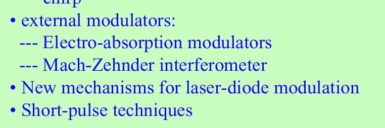
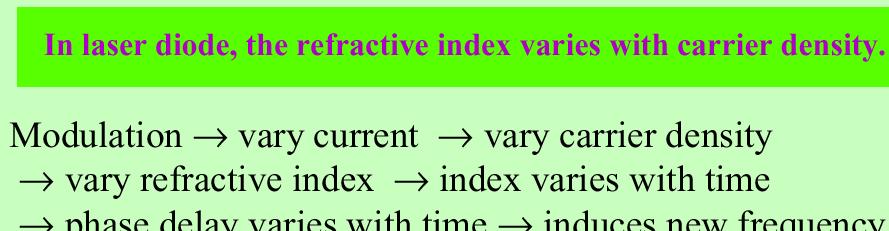
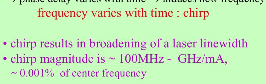
89 Limitations of Direct Modulation Turn on delay and resonance frequency are the two major factors that limit the speed of digital laser modulation Saturation and clipping introduces nonlinear distortion with analog modulation (especially in multi carrier systems) Nonlinear distortions introduce second and third order intermodulation products Chirp: Laser output wavelength drift with modulating current is also another issue, resulting in line broadening.
90 Chirp
.")
91 The Chirped Pulse A pulse can have a frequency that varies in time. This pulse increases its frequency linearly in time (from red to blue). In analogy to bird sounds, this pulse is called a "chirped" pulse.
92 Temperature variation of the threshold current I ( T ) = th I z e T / T 0
93 External Optical Modulation Laser Diode RF in EOM F ibre L ink Photo Detector RF out Modulation and light generation are separated Offers much wider bandwidth up to 60 GHz More expensive and complex Used in high end systems
94 External Modulated Spectrum Typical spectrum is double side band However, single side band is possible which is useful at extreme RF frequencies
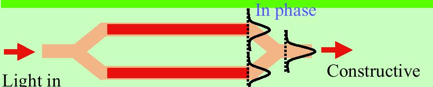
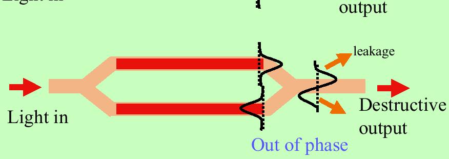
95 Mach-Zehnder Interferometers
96 Mach- Zehnder modulator

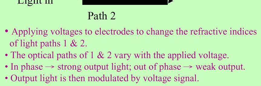
97 Mach- Zehnder modulator
98
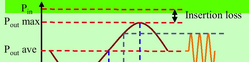
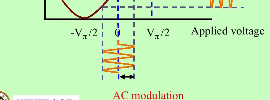
99

100 Characteristics of Mach- Zehnder modulator

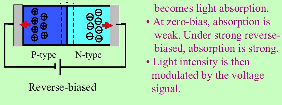
101 Electro- absorption (EA) modulator
 Laser: laser")

102 Integration of EA modulator with LD Quantum well (QW) Laser: laser diode whose active region is so narrow that quantum confinement occurs
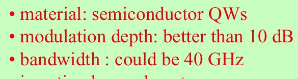

103 Characteristics of EA modulator
Review of Semiconductor Physics
 Review of Semiconductor Physics k B 1.38 u 10 23 JK -1 a) Energy level diagrams showing the excitation of an electron from the valence band to the conduction band. The resultant free electron can freely
Modulation of light. Direct modulation of sources Electro-absorption (EA) modulators
 modulators") Modulation of light Direct modulation of sources Electro-absorption (EA) modulators Why Modulation A communication link is established by transmission of information reliably Optical modulation is embedding
Modulation of light Direct modulation of sources Electro-absorption (EA) modulators Why Modulation A communication link is established by transmission of information reliably Optical modulation is embedding
Lecture 6 Fiber Optical Communication Lecture 6, Slide 1
 Lecture 6 Optical transmitters Photon processes in light matter interaction Lasers Lasing conditions The rate equations CW operation Modulation response Noise Light emitting diodes (LED) Power Modulation
Basic concepts. Optical Sources (b) Optical Sources (a) Requirements for light sources (b) Requirements for light sources (a)
 Optical Sources (a) Requirements for light sources (b) Requirements for light sources (a)") Optical Sources (a) Optical Sources (b) The main light sources used with fibre optic systems are: Light-emitting diodes (LEDs) Semiconductor lasers (diode lasers) Fibre laser and other compact solid-state
Optical Sources (a) Optical Sources (b) The main light sources used with fibre optic systems are: Light-emitting diodes (LEDs) Semiconductor lasers (diode lasers) Fibre laser and other compact solid-state
Optodevice Data Book ODE I. Rev.9 Mar Opnext Japan, Inc.
 Optodevice Data Book ODE-408-001I Rev.9 Mar. 2003 Opnext Japan, Inc. Section 1 Operating Principles 1.1 Operating Principles of Laser Diodes (LDs) and Infrared Emitting Diodes (IREDs) 1.1.1 Emitting Principles
Introduction Fundamentals of laser Types of lasers Semiconductor lasers
 ECE 5368 Introduction Fundamentals of laser Types of lasers Semiconductor lasers Introduction Fundamentals of laser Types of lasers Semiconductor lasers How many types of lasers? Many many depending on
ECE 340 Lecture 29 : LEDs and Lasers Class Outline:
 ECE 340 Lecture 29 : LEDs and Lasers Class Outline: Light Emitting Diodes Lasers Semiconductor Lasers Things you should know when you leave Key Questions What is an LED and how does it work? How does a
Key Questions. What is an LED and how does it work? How does a laser work? How does a semiconductor laser work? ECE 340 Lecture 29 : LEDs and Lasers
 Things you should know when you leave Key Questions ECE 340 Lecture 29 : LEDs and Class Outline: What is an LED and how does it How does a laser How does a semiconductor laser How do light emitting diodes
Figure 1. Schematic diagram of a Fabry-Perot laser.
 Figure 1. Schematic diagram of a Fabry-Perot laser. Figure 1. Shows the structure of a typical edge-emitting laser. The dimensions of the active region are 200 m m in length, 2-10 m m lateral width and
Lecture 4 Fiber Optical Communication Lecture 4, Slide 1
 Lecture 4 Optical transmitters Photon processes in light matter interaction Lasers Lasing conditions The rate equations CW operation Modulation response Noise Light emitting diodes (LED) Power Modulation
FIBER OPTICS. Prof. R.K. Shevgaonkar. Department of Electrical Engineering. Indian Institute of Technology, Bombay. Lecture: 18.
 FIBER OPTICS Prof. R.K. Shevgaonkar Department of Electrical Engineering Indian Institute of Technology, Bombay Lecture: 18 Optical Sources- Introduction to LASER Diodes Fiber Optics, Prof. R.K. Shevgaonkar,
Luminous Equivalent of Radiation
 Intensity vs λ Luminous Equivalent of Radiation When the spectral power (p(λ) for GaP-ZnO diode has a peak at 0.69µm) is combined with the eye-sensitivity curve a peak response at 0.65µm is obtained with
MAHALAKSHMI ENGINEERING COLLEGE TIRUCHIRAPALLI
 MAHALAKSHMI ENGINEERING COLLEGE TIRUCHIRAPALLI - 621213 DEPARTMENT : ECE SUBJECT NAME : OPTICAL COMMUNICATION & NETWORKS SUBJECT CODE : EC 2402 UNIT III: SOURCES AND DETECTORS PART -A (2 Marks) 1. What
UNIT-III SOURCES AND DETECTORS. According to the shape of the band gap as a function of the momentum, semiconductors are classified as
 UNIT-III SOURCES AND DETECTORS DIRECT AND INDIRECT BAND GAP SEMICONDUCTORS: According to the shape of the band gap as a function of the momentum, semiconductors are classified as 1. Direct band gap semiconductors
Semiconductor Optical Communication Components and Devices Lecture 18: Introduction to Diode Lasers - I
 Semiconductor Optical Communication Components and Devices Lecture 18: Introduction to Diode Lasers - I Prof. Utpal Das Professor, Department of lectrical ngineering, Laser Technology Program, Indian Institute
Lecture 9 External Modulators and Detectors
 Optical Fibres and Telecommunications Lecture 9 External Modulators and Detectors Introduction Where are we? A look at some real laser diodes. External modulators Mach-Zender Electro-absorption modulators
Semiconductor Lasers Semiconductors were originally pumped by lasers or e-beams First diode types developed in 1962: Create a pn junction in
 Semiconductor Lasers Semiconductors were originally pumped by lasers or e-beams First diode types developed in 1962: Create a pn junction in semiconductor material Pumped now with high current density
LASER DIODE MODULATION AND NOISE
 > 5' O ft I o Vi LASER DIODE MODULATION AND NOISE K. Petermann lnstitutfiir Hochfrequenztechnik, Technische Universitdt Berlin Kluwer Academic Publishers i Dordrecht / Boston / London KTK Scientific Publishers
Lecture 18: Photodetectors
 Lecture 18: Photodetectors Contents 1 Introduction 1 2 Photodetector principle 2 3 Photoconductor 4 4 Photodiodes 6 4.1 Heterojunction photodiode.................... 8 4.2 Metal-semiconductor photodiode................
Light Sources, Modulation, Transmitters and Receivers
 Optical Fibres and Telecommunications Light Sources, Modulation, Transmitters and Receivers Introduction Previous section looked at Fibres. How is light generated in the first place? How is light modulated?
Laser Diode. Photonic Network By Dr. M H Zaidi
 Laser Diode Light emitters are a key element in any fiber optic system. This component converts the electrical signal into a corresponding light signal that can be injected into the fiber. The light emitter
Physics of Waveguide Photodetectors with Integrated Amplification
 Physics of Waveguide Photodetectors with Integrated Amplification J. Piprek, D. Lasaosa, D. Pasquariello, and J. E. Bowers Electrical and Computer Engineering Department University of California, Santa
Optical Sources and Detectors
 Optical Sources and Detectors 1. Optical Sources Optical transmitter coverts electrical input signal into corresponding optical signal. The optical signal is then launched into the fiber. Optical source
Optoelectronics EE/OPE 451, OPT 444 Fall 2009 Section 1: T/Th 9:30-10:55 PM
 Optoelectronics EE/OPE 451, OPT 444 Fall 009 Section 1: T/Th 9:30-10:55 PM John D. Williams, Ph.D. Department of Electrical and Computer Engineering 406 Optics Building - UAHuntsville, Huntsville, AL 35899
Application Instruction 002. Superluminescent Light Emitting Diodes: Device Fundamentals and Reliability
 I. Introduction II. III. IV. SLED Fundamentals SLED Temperature Performance SLED and Optical Feedback V. Operation Stability, Reliability and Life VI. Summary InPhenix, Inc., 25 N. Mines Road, Livermore,
Semiconductor Lasers Semiconductors were originally pumped by lasers or e-beams First diode types developed in 1962: Create a pn junction in
 Semiconductor Lasers Semiconductors were originally pumped by lasers or e-beams First diode types developed in 1962: Create a pn junction in semiconductor material Pumped now with high current density
Chapter 3 OPTICAL SOURCES AND DETECTORS
 Chapter 3 OPTICAL SOURCES AND DETECTORS 3. Optical sources and Detectors 3.1 Introduction: The success of light wave communications and optical fiber sensors is due to the result of two technological breakthroughs.
Optical MEMS in Compound Semiconductors Advanced Engineering Materials, Cal Poly, SLO November 16, 2007
 Optical MEMS in Compound Semiconductors Advanced Engineering Materials, Cal Poly, SLO November 16, 2007 Outline Brief Motivation Optical Processes in Semiconductors Reflectors and Optical Cavities Diode
Ph 77 ADVANCED PHYSICS LABORATORY ATOMIC AND OPTICAL PHYSICS
 Ph 77 ADVANCED PHYSICS LABORATORY ATOMIC AND OPTICAL PHYSICS Diode Laser Characteristics I. BACKGROUND Beginning in the mid 1960 s, before the development of semiconductor diode lasers, physicists mostly
Optical Amplifiers (Chapter 6)
") Optical Amplifiers (Chapter 6) General optical amplifier theory Semiconductor Optical Amplifier (SOA) Raman Amplifiers Erbium-doped Fiber Amplifiers (EDFA) Read Chapter 6, pp. 226-266 Loss & dispersion
Optical Amplifiers (Chapter 6) General optical amplifier theory Semiconductor Optical Amplifier (SOA) Raman Amplifiers Erbium-doped Fiber Amplifiers (EDFA) Read Chapter 6, pp. 226-266 Loss & dispersion
Optical Amplifiers. Continued. Photonic Network By Dr. M H Zaidi
 Optical Amplifiers Continued EDFA Multi Stage Designs 1st Active Stage Co-pumped 2nd Active Stage Counter-pumped Input Signal Er 3+ Doped Fiber Er 3+ Doped Fiber Output Signal Optical Isolator Optical
OPTOELECTRONIC and PHOTOVOLTAIC DEVICES
 OPTOELECTRONIC and PHOTOVOLTAIC DEVICES Outline 1. Introduction to the (semiconductor) physics: energy bands, charge carriers, semiconductors, p-n junction, materials, etc. 2. Light emitting diodes Light
R. J. Jones Optical Sciences OPTI 511L Fall 2017
 R. J. Jones Optical Sciences OPTI 511L Fall 2017 Semiconductor Lasers (2 weeks) Semiconductor (diode) lasers are by far the most widely used lasers today. Their small size and properties of the light output
CONTENTS. Chapter 1 Wave Nature of Light 19
 CONTENTS Chapter 1 Wave Nature of Light 19 1.1 Light Waves in a Homogeneous Medium 19 A. Plane Electromagnetic Wave 19 B. Maxwell's Wave Equation and Diverging Waves 22 Example 1.1.1 A diverging laser
White Paper Laser Sources For Optical Transceivers. Giacomo Losio ProLabs Head of Technology
 White Paper Laser Sources For Optical Transceivers Giacomo Losio ProLabs Head of Technology September 2014 Laser Sources For Optical Transceivers Optical transceivers use different semiconductor laser
Semiconductor Optical Communication Components and Devices Lecture 39: Optical Modulators
 Semiconductor Optical Communication Components and Devices Lecture 39: Optical Modulators Prof. Utpal Das Professor, Department of Electrical Engineering, Laser Technology Program, Indian Institute of
LASER Transmitters 1 OBJECTIVE 2 PRE-LAB
 LASER Transmitters 1 OBJECTIVE Investigate the L-I curves and spectrum of a FP Laser and observe the effects of different cavity characteristics. Learn to perform parameter sweeps in OptiSystem. 2 PRE-LAB
Safa O. Kasap Electrical Engineering Department, University of Saskatchewan, Saskatoon, S7N 5A9, Canada
 1 Optoelectronics Safa O. Kasap Electrical Engineering Department, University of Saskatchewan, Saskatoon, S7N 5A9, Canada e-mail: kasap@engr.usask.ca Abstract It is useful to view today s optoelectronics
Examination Optoelectronic Communication Technology. April 11, Name: Student ID number: OCT1 1: OCT 2: OCT 3: OCT 4: Total: Grade:
 Examination Optoelectronic Communication Technology April, 26 Name: Student ID number: OCT : OCT 2: OCT 3: OCT 4: Total: Grade: Declaration of Consent I hereby agree to have my exam results published on
S Optical Networks Course Lecture 2: Essential Building Blocks
 S-72.3340 Optical Networks Course Lecture 2: Essential Building Blocks Edward Mutafungwa Communications Laboratory, Helsinki University of Technology, P. O. Box 2300, FIN-02015 TKK, Finland Tel: +358 9
Optoelectronics ELEC-E3210
 Optoelectronics ELEC-E3210 Lecture 4 Spring 2016 Outline 1 Lateral confinement: index and gain guiding 2 Surface emitting lasers 3 DFB, DBR, and C3 lasers 4 Quantum well lasers 5 Mode locking P. Bhattacharya:
CONTENTS. 2.2 Schrodinger's Wave Equation 31. PART I Semiconductor Material Properties. 2.3 Applications of Schrodinger's Wave Equation 34
 CONTENTS Preface x Prologue Semiconductors and the Integrated Circuit xvii PART I Semiconductor Material Properties CHAPTER 1 The Crystal Structure of Solids 1 1.0 Preview 1 1.1 Semiconductor Materials
Notes on Optical Amplifiers
 Notes on Optical Amplifiers Optical amplifiers typically use energy transitions such as those in atomic media or electron/hole recombination in semiconductors. In optical amplifiers that use semiconductor
Electronic devices-i. Difference between conductors, insulators and semiconductors
 Electronic devices-i Semiconductor Devices is one of the important and easy units in class XII CBSE Physics syllabus. It is easy to understand and learn. Generally the questions asked are simple. The unit
UNIT What is splicing? Explain about fusion splicing? Ans: Splicing
 UNIT 4 1. What is splicing? Explain about fusion splicing? Ans: Splicing A permanent joint formed between two individual optical fibers in the field is known as splicing. The fiber splicing is used to
Optical Receivers Theory and Operation
 Optical Receivers Theory and Operation Photo Detectors Optical receivers convert optical signal (light) to electrical signal (current/voltage) Hence referred O/E Converter Photodetector is the fundamental
Chapter 8. Wavelength-Division Multiplexing (WDM) Part II: Amplifiers
 Part II: Amplifiers") Chapter 8 Wavelength-Division Multiplexing (WDM) Part II: Amplifiers Introduction Traditionally, when setting up an optical link, one formulates a power budget and adds repeaters when the path loss exceeds
Chapter 8 Wavelength-Division Multiplexing (WDM) Part II: Amplifiers Introduction Traditionally, when setting up an optical link, one formulates a power budget and adds repeaters when the path loss exceeds
CHAPTER 8 The PN Junction Diode
 CHAPTER 8 The PN Junction Diode Consider the process by which the potential barrier of a PN junction is lowered when a forward bias voltage is applied, so holes and electrons can flow across the junction
Ultralow-power all-optical RAM based on nanocavities
 Supplementary information SUPPLEMENTARY INFORMATION Ultralow-power all-optical RAM based on nanocavities Kengo Nozaki, Akihiko Shinya, Shinji Matsuo, Yasumasa Suzaki, Toru Segawa, Tomonari Sato, Yoshihiro
TECHNICAL BRIEF O K I L A S E R D I O D E P R O D U C T S. OKI Laser Diodes
 TECHNICAL BRIEF O K I L A S E R D I O D E P R O D U C T S OKI Laser Diodes June 1995 OKI Laser Diodes INTRODUCTION This technical brief presents an overview of OKI laser diode and edge emitting light emitting
Chapter 1 Introduction
 Chapter 1 Introduction 1-1 Preface Telecommunication lasers have evolved substantially since the introduction of the early AlGaAs-based semiconductor lasers in the late 1970s suitable for transmitting
Department of Electrical Engineering IIT Madras
 Department of Electrical Engineering IIT Madras Sample Questions on Semiconductor Devices EE3 applicants who are interested to pursue their research in microelectronics devices area (fabrication and/or
Optical Fibers p. 1 Basic Concepts p. 1 Step-Index Fibers p. 2 Graded-Index Fibers p. 4 Design and Fabrication p. 6 Silica Fibers p.
 Preface p. xiii Optical Fibers p. 1 Basic Concepts p. 1 Step-Index Fibers p. 2 Graded-Index Fibers p. 4 Design and Fabrication p. 6 Silica Fibers p. 6 Plastic Optical Fibers p. 9 Microstructure Optical
LEDs, Photodetectors and Solar Cells
 LEDs, Photodetectors and Solar Cells Chapter 7 (Parker) ELEC 424 John Peeples Why the Interest in Photons? Answer: Momentum and Radiation High electrical current density destroys minute polysilicon and
Lasers PH 645/ OSE 645/ EE 613 Summer 2010 Section 1: T/Th 2:45-4:45 PM Engineering Building 240
 Lasers PH 645/ OSE 645/ EE 613 Summer 2010 Section 1: T/Th 2:45-4:45 PM Engineering Building 240 John D. Williams, Ph.D. Department of Electrical and Computer Engineering 406 Optics Building - UAHuntsville,
ECEN689: Special Topics in Optical Interconnects Circuits and Systems Spring 2016
 ECEN689: Special Topics in Optical Interconnects Circuits and Systems Spring 016 Lecture 7: Transmitter Analysis Sam Palermo Analog & Mixed-Signal Center Texas A&M University Optical Modulation Techniques
21. (i) Briefly explain the evolution of fiber optic system (ii) Compare the configuration of different types of fibers. or 22. (b)(i) Derive modal eq
 Briefly explain the evolution of fiber optic system (ii) Compare the configuration of different types of fibers. or 22. (b)(i) Derive modal eq") Unit-1 Part-A FATIMA MICHAEL COLLEGE OF ENGINEERING & TECHNOLOGY Senkottai Village, Madurai Sivagangai Main Road, Madurai - 625 020. [An ISO 9001:2008 Certified Institution] DEPARTMENT OF ELECTRONICS AND
Unit-1 Part-A FATIMA MICHAEL COLLEGE OF ENGINEERING & TECHNOLOGY Senkottai Village, Madurai Sivagangai Main Road, Madurai - 625 020. [An ISO 9001:2008 Certified Institution] DEPARTMENT OF ELECTRONICS AND
Lecture 5: Introduction to Lasers
 Lecture 5: Introduction to Lasers http://en.wikipedia.org/wiki/laser History of the Laser v Invented in 1958 by Charles Townes (Nobel prize in Physics 1964) and Arthur Schawlow of Bell Laboratories v Was
BN 1000 May Profile Optische Systeme GmbH Gauss Str. 11 D Karlsfeld / Germany. Tel Fax
 BN 1000 May 2000 Profile Optische Systeme GmbH Gauss Str. 11 D - 85757 Karlsfeld / Germany Tel + 49 8131 5956-0 Fax + 49 8131 5956-99 info@profile-optsys.com www.profile-optsys.com Profile Inc. 87 Hibernia
A new picosecond Laser pulse generation method.
 PULSE GATING : A new picosecond Laser pulse generation method. Picosecond lasers can be found in many fields of applications from research to industry. These lasers are very common in bio-photonics, non-linear
VERTICAL CAVITY SURFACE EMITTING LASER
 VERTICAL CAVITY SURFACE EMITTING LASER Nandhavel International University Bremen 1/14 Outline Laser action, optical cavity (Fabry Perot, DBR and DBF) What is VCSEL? How does VCSEL work? How is it different
NEW YORK CITY COLLEGE of TECHNOLOGY
 NEW YORK CITY COLLEGE of TECHNOLOGY THE CITY UNIVERSITY OF NEW YORK DEPARTMENT OF ELECTRICAL AND TELECOMMUNICATIONS ENGINEERING TECHNOLOGY Course : TCET 4102 (TC 700) Fiber-optic communications Module
The electric field for the wave sketched in Fig. 3-1 can be written as
 ELECTROMAGNETIC WAVES Light consists of an electric field and a magnetic field that oscillate at very high rates, of the order of 10 14 Hz. These fields travel in wavelike fashion at very high speeds.
Lecture 4 INTEGRATED PHOTONICS
 Lecture 4 INTEGRATED PHOTONICS What is photonics? Photonic applications use the photon in the same way that electronic applications use the electron. Devices that run on light have a number of advantages
1 Semiconductor-Photon Interaction
 1 SEMICONDUCTOR-PHOTON INTERACTION 1 1 Semiconductor-Photon Interaction Absorption: photo-detectors, solar cells, radiation sensors. Radiative transitions: light emitting diodes, displays. Stimulated emission:
DIRECT MODULATION WITH SIDE-MODE INJECTION IN OPTICAL CATV TRANSPORT SYSTEMS
 Progress In Electromagnetics Research Letters, Vol. 11, 73 82, 2009 DIRECT MODULATION WITH SIDE-MODE INJECTION IN OPTICAL CATV TRANSPORT SYSTEMS W.-J. Ho, H.-H. Lu, C.-H. Chang, W.-Y. Lin, and H.-S. Su
Vertical External Cavity Surface Emitting Laser
 Chapter 4 Optical-pumped Vertical External Cavity Surface Emitting Laser The booming laser techniques named VECSEL combine the flexibility of semiconductor band structure and advantages of solid-state
Fiber-Optic Communication Systems
 Fiber-Optic Communication Systems Second Edition GOVIND P. AGRAWAL The Institute of Optics University of Rochester Rochester, NY A WILEY-iNTERSCIENCE PUBLICATION JOHN WILEY & SONS, INC. NEW YORK / CHICHESTER
Wavelength switching using multicavity semiconductor laser diodes
 Wavelength switching using multicavity semiconductor laser diodes A. P. Kanjamala and A. F. J. Levi Department of Electrical Engineering University of Southern California Los Angeles, California 989-1111
Detectors for Optical Communications
 Optical Communications: Circuits, Systems and Devices Chapter 3: Optical Devices for Optical Communications lecturer: Dr. Ali Fotowat Ahmady Sep 2012 Sharif University of Technology 1 Photo All detectors
Advanced semiconductor lasers
 Advanced semiconductor lasers Quantum cascade lasers Single mode lasers DFBs, VCSELs, etc. Quantum cascade laser Reminder: Semiconductor laser diodes Conventional semiconductor laser CB diode laser: material
Problem 4 Consider a GaAs p-n + junction LED with the following parameters at 300 K: Electron diusion coecient, D n = 25 cm 2 =s Hole diusion coecient
 Prof. Jasprit Singh Fall 2001 EECS 320 Homework 7 This homework is due on November 8. Problem 1 An optical power density of 1W/cm 2 is incident on a GaAs sample. The photon energy is 2.0 ev and there is
InP-based Waveguide Photodetector with Integrated Photon Multiplication
 InP-based Waveguide Photodetector with Integrated Photon Multiplication D.Pasquariello,J.Piprek,D.Lasaosa,andJ.E.Bowers Electrical and Computer Engineering Department University of California, Santa Barbara,
Fiberoptic Communication Systems By Dr. M H Zaidi. Optical Amplifiers
 Optical Amplifiers Optical Amplifiers Optical signal propagating in fiber suffers attenuation Optical power level of a signal must be periodically conditioned Optical amplifiers are a key component in
Absorption: in an OF, the loss of Optical power, resulting from conversion of that power into heat.
 Absorption: in an OF, the loss of Optical power, resulting from conversion of that power into heat. Scattering: The changes in direction of light confined within an OF, occurring due to imperfection in
FET Channel. - simplified representation of three terminal device called a field effect transistor (FET)
") FET Channel - simplified representation of three terminal device called a field effect transistor (FET) - overall horizontal shape - current levels off as voltage increases - two regions of operation 1.
FET Channel - simplified representation of three terminal device called a field effect transistor (FET) - overall horizontal shape - current levels off as voltage increases - two regions of operation 1.
EE 230: Optical Fiber Communication Transmitters
 EE 230: Optical Fiber Communication Transmitters From the movie Warriors of the Net Laser Diode Structures Most require multiple growth steps Thermal cycling is problematic for electronic devices Fabry
Design of InGaAs/InP 1.55μm vertical cavity surface emitting lasers (VCSEL)
") Design of InGaAs/InP 1.55μm vertical cavity surface emitting lasers (VCSEL) J.-M. Lamy, S. Boyer-Richard, C. Levallois, C. Paranthoën, H. Folliot, N. Chevalier, A. Le Corre, S. Loualiche UMR FOTON 6082
Design of InGaAs/InP 1.55μm vertical cavity surface emitting lasers (VCSEL) J.-M. Lamy, S. Boyer-Richard, C. Levallois, C. Paranthoën, H. Folliot, N. Chevalier, A. Le Corre, S. Loualiche UMR FOTON 6082
Photonics and Fiber Optics
 1 UNIT V Photonics and Fiber Optics Part-A 1. What is laser? LASER is the acronym for Light Amplification by Stimulated Emission of Radiation. The absorption and emission of light by materials has been
DIODE LASER SPECTROSCOPY (160309)
") DIODE LASER SPECTROSCOPY (160309) Introduction The purpose of this laboratory exercise is to illustrate how we may investigate tiny energy splittings in an atomic system using laser spectroscopy. As an
DIODE LASER SPECTROSCOPY (160309) Introduction The purpose of this laboratory exercise is to illustrate how we may investigate tiny energy splittings in an atomic system using laser spectroscopy. As an
 Electronic Devices 1. Current flowing in each of the following circuits A and respectively are: (Circuit 1) (Circuit 2) 1) 1A, 2A 2) 2A, 1A 3) 4A, 2A 4) 2A, 4A 2. Among the following one statement is not
Optical Amplifiers Photonics and Integrated Optics (ELEC-E3240) Zhipei Sun Photonics Group Department of Micro- and Nanosciences Aalto University
 Zhipei Sun Photonics Group Department of Micro- and Nanosciences Aalto University") Photonics Group Department of Micro- and Nanosciences Aalto University Optical Amplifiers Photonics and Integrated Optics (ELEC-E3240) Zhipei Sun Last Lecture Topics Course introduction Ray optics & optical
Photonics Group Department of Micro- and Nanosciences Aalto University Optical Amplifiers Photonics and Integrated Optics (ELEC-E3240) Zhipei Sun Last Lecture Topics Course introduction Ray optics & optical
15 Transit Time and Tunnel NDR Devices
 15 Transit Time and Tunnel NDR Devices Schematics of Transit-time NDR diode. A packet of carriers (e.g., electrons) is generated in a confined and narrow zone (generation region) and injected into the
Downloaded from
 SOLID AND SEMICONDUCTOR DEVICES (EASY AND SCORING TOPIC) 1. Distinction of metals, semiconductor and insulator on the basis of Energy band of Solids. 2. Types of Semiconductor. 3. PN Junction formation
Coherent Receivers Principles Downconversion
 Coherent Receivers Principles Downconversion Heterodyne receivers mix signals of different frequency; if two such signals are added together, they beat against each other. The resulting signal contains
DEVELOPMENT OF A NEW INJECTION LOCKING RING LASER AMPLIFIER USING A COUNTER INJECTION: MULTIWAVELENGTH AMPLIFICATION
 DEVELOPMENT OF A NEW INJECTION LOCKING RING LASER AMPLIFIER USING A COUNTER INJECTION: MULTAVELENGTH AMPLIFICATION Rosen Vanyuhov Peev 1, Margarita Anguelova Deneva 1, Marin Nenchev Nenchev 1,2 1 Dept.
Guided Propagation Along the Optical Fiber. Xavier Fernando Ryerson University
 Guided Propagation Along the Optical Fiber Xavier Fernando Ryerson University The Nature of Light Quantum Theory Light consists of small particles (photons) Wave Theory Light travels as a transverse electromagnetic
Spatial Investigation of Transverse Mode Turn-On Dynamics in VCSELs
 Spatial Investigation of Transverse Mode Turn-On Dynamics in VCSELs Safwat W.Z. Mahmoud Data transmission experiments with single-mode as well as multimode 85 nm VCSELs are carried out from a near-field
A continuous-wave Raman silicon laser
 A continuous-wave Raman silicon laser Haisheng Rong, Richard Jones,.. - Intel Corporation Ultrafast Terahertz nanoelectronics Lab Jae-seok Kim 1 Contents 1. Abstract 2. Background I. Raman scattering II.
Lecture 19 Optical Characterization 1
 Lecture 19 Optical Characterization 1 1/60 Announcements Homework 5/6: Is online now. Due Wednesday May 30th at 10:00am. I will return it the following Wednesday (6 th June). Homework 6/6: Will be online
Fibre Optic Sensors: basic principles and most common applications
 SMR 1829-21 Winter College on Fibre Optics, Fibre Lasers and Sensors 12-23 February 2007 Fibre Optic Sensors: basic principles and most common applications (PART 2) Hypolito José Kalinowski Federal University
Moderne Teilchendetektoren - Theorie und Praxis 2. Dr. Bernhard Ketzer Technische Universität München SS 2013
 Moderne Teilchendetektoren - Theorie und Praxis 2 Dr. Bernhard Ketzer Technische Universität München SS 2013 7 Signal Processing and Acquisition 7.1 Signals 7.2 Amplifier 7.3 Electronic Noise 7.4 Analog-to-Digital
Semiconductor Optoelectronics Prof. M. R. Shenoy Department of Physics Indian Institute of Technology, Delhi
 Semiconductor Optoelectronics Prof. M. R. Shenoy Department of Physics Indian Institute of Technology, Delhi Lecture - 26 Semiconductor Optical Amplifier (SOA) (Refer Slide Time: 00:39) Welcome to this
Chapter 8. Digital Links
 Chapter 8 Digital Links Point-to-point Links Link Power Budget Rise-time Budget Power Penalties Dispersions Noise Content Photonic Digital Link Analysis & Design Point-to-Point Link Requirement: - Data
CHAPTER 8 The PN Junction Diode
 CHAPTER 8 The PN Junction Diode Consider the process by which the potential barrier of a PN junction is lowered when a forward bias voltage is applied, so holes and electrons can flow across the junction
Intrinsic Semiconductor
 Semiconductors Crystalline solid materials whose resistivities are values between those of conductors and insulators. Good electrical characteristics and feasible fabrication technology are some reasons
Guided Propagation Along the Optical Fiber. Xavier Fernando Ryerson Comm. Lab
 Guided Propagation Along the Optical Fiber Xavier Fernando Ryerson Comm. Lab The Nature of Light Quantum Theory Light consists of small particles (photons) Wave Theory Light travels as a transverse electromagnetic
Low threshold continuous wave Raman silicon laser
 NATURE PHOTONICS, VOL. 1, APRIL, 2007 Low threshold continuous wave Raman silicon laser HAISHENG RONG 1 *, SHENGBO XU 1, YING-HAO KUO 1, VANESSA SIH 1, ODED COHEN 2, OMRI RADAY 2 AND MARIO PANICCIA 1 1:
Nd:YSO resonator array Transmission spectrum (a. u.) Supplementary Figure 1. An array of nano-beam resonators fabricated in Nd:YSO.
 Supplementary Figure 1. An array of nano-beam resonators fabricated in Nd:YSO.") a Nd:YSO resonator array µm Transmission spectrum (a. u.) b 4 F3/2-4I9/2 25 2 5 5 875 88 λ(nm) 885 Supplementary Figure. An array of nano-beam resonators fabricated in Nd:YSO. (a) Scanning electron microscope
a Nd:YSO resonator array µm Transmission spectrum (a. u.) b 4 F3/2-4I9/2 25 2 5 5 875 88 λ(nm) 885 Supplementary Figure. An array of nano-beam resonators fabricated in Nd:YSO. (a) Scanning electron microscope
Solid-State Laser Engineering
 Walter Koechner Solid-State Laser Engineering Fourth Extensively Revised and Updated Edition With 449 Figures Springer Contents 1. Introduction 1 1.1 Optical Amplification 1 1.2 Interaction of Radiation