Design of A Fast Lock-in All-Digital Phase-Locked Loop in 40-nm CMOS Technology
|
|
|
- Violet Davidson
- 5 years ago
- Views:
Transcription
1 國立中正大學 資訊工程研究所碩士論文 40 奈米製程下開發與設計快速鎖定之 全數位鎖相迴路 Design of A Fast Lock-in All-Digital Phase-Locked Loop in 40-nm CMOS Technology 研究生 : 指導教授 : 羅啟光 鍾菁哲博士 中華民國一零四年七月 - I -
2 - I -
3 - II -
4 - III -
5 摘要 近年來, 系統晶片 (SoC) 被廣泛的應用在生醫電子 展頻電路 植入式醫療裝置以及無線網路等應用, 由於在 SoC 中, 需要供應不同頻率的工作時脈到不同 I/O 介面, 因此, 鎖相迴路 (PLLs) 經常使用在 SoC 上, 以產生多組不同的工作時脈 此外, 這些應用的需求在於低耗能及低成本 隨著先進 CMOS 製程的開發, 工作電壓不斷的下降, 傳統 PLL 在設計上遭遇很大的挑戰 基於 time to market 的考量, 為了減少重新設計 PLL 的時間與努力,ADPLL 採用了全數位的設計方式, 以及使用標準元件 (Standard Cell) 實現 ADPLL, 不僅加速了設計過程, 更增加 PLL 的移植性, 相較於傳統 PLL, 全數位鎖相迴路 (ADPLL) 更適合用於 SoC 上 由於傳統 PLL 的鎖定時間都很長, 導致 PLL 需要較長的工作時間 當系統待命時,PLL 的耗能即成為 SoC 待機 (Standby) 時功率消耗的主要來源 因此, 若縮短 PLL 的鎖定時間, 即早鎖定頻率及相位,PLL 便可隨需求關閉以減少耗能, 快速鎖定的 ADPLL 變成設計的趨勢 因此, 在本文中, 我們提出快速鎖定的全數位鎖相迴路, 透過校正及補償機制來降低面積成本的消耗, 以及提升鎖定中心頻率的精準度, 是本論文的主要目的及貢獻 本論文以 40 奈米製程標準元件庫實現, 並驗證我們所提出的電路架構 關鍵字 : 全數位鎖相迴路 快速鎖定全數位鎖相迴路 - II -
6 Abstract In recent years, biomedical electronic applications, spread-spectrum clock generators, implantable medical devices, and frequency hopping wireless applications are widely used in system-on-a-chip (SoC). In an SoC, it requires different clock sources for different I/O interfaces. Thus, phase-locked loops play an important role in SoC in order to generate different clock sources. Besides, the primary concern of these applications are low energy and low cost. While the operation voltage is scaling down with the latest CMOS process, analog PLLs encounter great design challenges. According to time to market, in order to minimize the design time and the design efforts, all-digital phase-locked loops (ADPLLs) are adopted in digital design approaches. In addition, ADPLLs implemented with standard cells can not only speed up the design time, but also improve the portability. As compared with analog PLLs, ADPLLs are more suitable for SoC. Analog PLLs are usually not to be stopped due to the long lock-in time. When the system is in sleeping mode, the PLL power consumption dominates the standby power consumption of the system. Therefore, if PLLs can lock the frequency and phase quickly, the lock-in time can be reduced so that PLLs can be turned off in low power modes. As a result, fast lock-in ADPLLs become more and more popular. Therefore, in this thesis, we proposed a fast lock-in ADPLL with a calibration method in order to decrease the chip area and improve the accuracy in frequency estimation. In addition, the test chip is implemented and verified in TSMC 40-nm CMOS process with standard cells. Keywords:All-Digital Phase-Locked Loop (ADPLL), Fast Lock-in ADPLL - III -
7 Acknowledgments I would like to express the deepest gratitude to my advisor, Prof. Ching-Che Chung. He always gives me the right direction and enthusiastic guidance, and helps me to complete my research. I would like to thank to my partners of Silicon Sensor and System (S3) Lab of National Chung Chen University, too. Without their assistance, I could not overcome many difficulties over two years. Finally, I would like to thank my family and my girlfriend, who always concern for me. This really makes me to be optimistic every time. - IV -
8 Content Abstract III Content V List of Figures... VI List of Tables... VIII Chapter 1 Introduction Why the Feature of Fast Lock-in is Required in ADPLL Conventional Fast Lock-in Methods Survey Binary Search Algorithm Gear Shifting Frequency Counter Based Approach Frequency Estimation Algorithm Phase Calibration Summary Thesis Organization Chapter 2 Fast Lock-in All Digital Phase Locked Loop The Proposed Fast Lock-in ADPLL The Proposed Frequency Estimation Algorithm Summary Chapter 3 Circuit Design and Implementation of ADPLL Monotonic Digital Controlled Oscillator Design Coarse-Tuning Stage Fine-Tuning Stage The Proposed Regular Placement Method Phase and Frequency Detector Test Chip Implementation Digital Loop Filter Chapter 4 Full Chip Experimental Results Specifications Simulation Results Test Mode Simulation Chip Summary Table of Comparison Chapter 5 Conclusion and Future Works Conclusion V -
9 5.2 Future Works References List of Figures Fig. 1.1: ADPLL Architecture Fig. 1.2: Binary Search Algorithm Fig. 1.3: Modified Binary Search Algorithm Fig. 1.4: Modes of the Gear-Shifting Algorithm Fig. 1.5: Block Diagram of the Loop Filter Fig. 1.6: Architecture of Modified Bang-Bang Algorithm-Based ADPLL Fig. 1.7: Step Response of the ADPLL under Different Loop Filter Parameters Fig. 1.8: Architecture of TDC [17] Fig. 1.9: Architecture of 2-level flash TDC Fig. 1.10: Architecture of ADPLL [18] Fig. 1.11: FEA-Based Frequency Synthesizer Architecture Fig. 1.12: Cyclic TDC embedded DCO Fig. 1.13: Example of the Regula Falsi Method Fig. 1.14: Worst case of the Regula Falsi Method Fig. 1.15: Example of Locking Process in [13] Fig. 1.16: The Flowchart of ADPLL in [13] Fig. 1.17: Single-Shot Phase Synchronizer Schematic Fig. 1.18: Block Diagram of Phase Error Compensation Fig. 1.19: Compensating Timing Diagram Fig. 1.20: Architecture of the Phase Sync Scheme Fig. 1.21: Schematic of Lock Detector Fig. 1.22: Initializing DCO Timing Diagram Fig. 2.1: The Block Diagram of the Proposed ADPLL Fig. 2.2: Timing Diagram of the Proposed ADPLL Fig. 2.3: The relationship of R value and W value Fig. 2.4: The Relationship of the DCO Control Code and the W Value VI -
10 Fig. 2.5: The Quantization Error of the W Value without TDC Fig. 2.6: The Relationship between the Trapezoid Simulation W and the Compensate W line Fig. 2.7: The W Value Before Calibration and After Calibration Fig. 2.8: The Frequency Analysis at 260MHz Fig. 2.9: The frequency error Analysis with 150MHz Fig. 2.10: The initial frequency error between the proposed ADPLL and [4] Fig. 2.11: The initial frequency error between proposed and [10] Fig. 3.1: The Proposed DCO Fig. 3.2: The Proposed Coarse-Tuning Stage Fig. 3.3: The Coarse-Tuning Stage Delay Path Fig. 3.4: The Fine-Tuning Stage of the Proposed DCO Fig. 3.5: The Timing Diagram of the Fine-Tuning Interpolation Signal Illustration Fig. 3.6: The Regular Placement of the DCO Fig. 3.7: DNL Comparison of the DCO in μm Fig. 3.8: The Proposed phase and frequency detector Fig. 3.9: The Digital Pulse Amplifier Architecture Fig. 3.10: Frequency Divider Architecture Fig. 3.11: The Phase Error between REF_CLK and OUT_DIV_CLK Illustration Fig. 3.12: ADPLL Frequency Tracking Procedure Fig. 3.13: The Digital Loop Filter Structure [43] Fig. 4.1: (a) Layout of the Test Chip without the Dummy cell (b) Layout of the Test Chip with the Dummy cell (c) Layout of the Test Chip with the Bonding Pad Fig. 4.2: Chip Floorplan and I/O Plan Fig. 4.3: System Simulation of the proposed ADPLL with various test modes Fig. 4.4: System Simulation of the proposed ADPLL with PVT Variation VII -
11 List of Tables Table 1.1: An Example of Binary Search Algorithm in [15]... 6 Table 1.2: Comparison Table of Fast Lock-in Methods Table 3.1: The DCO Duty Cycle in 40-nm CMOS Process Table 3.2: The Frequency Range in Different Operating Voltage Table 4.1: Block Module Name Table 4.2: I/O PAD Description Table 4.3: Chip Summary Table 4.4: The DCO Simulation with Different Frequencies Table 4.5: Simulation with PVT Variations Table 4.6: Performance Comparison Table with Prior Design Table 4.7: Performance Comparison Table VIII -
12 Chapter 1 Introduction 1.1 Why the Feature of Fast Lock-in is Required in ADPLL In recent years, phase-locked loop (PLL) plays an important role in system-on-chip (SoC). In an SoC, it usually requires several PLLs to provide different clock sources for different I/O interfaces. PLLs generate various frequencies to apply to different applications and it is widely used in mobile communication system, wireless communication system and biomedical electronic. Traditionally, PLL is implemented by a charge-pump phase-locked loop which faces design challenge of leakage current in advanced CMOS process. Besides, the gain of voltage controlled oscillator (K VCO ) becomes larger due to the narrower range of the control voltage. Thus it easily suffers from noise on the control voltage. Traditional PLLs contain some passive components to design an analog loop filter that occupies huge chip area and has higher chip cost. Traditional PLLs also have a long lock-in time and have high power consumption. Therefore, in the era of the nano-scale process, PLLs which consist of a VCO, a charge-pump and an analog loop filter are not suitable for SoC that demands low power, low voltage operation, low chip area and especially requires fast locking [18]
13 Fig. 1.1: ADPLL Architecture. An all-digital phase-locked loop (ADPLL) takes the advantages of CMOS process as shown in Fig Compared with the traditional PLL, the ADPLL replaces passive components with the digital circuits, a VCO to a digital-controlled oscillator (DCO), and an analog filter to a digital filter. The chip size is reduced and the chip cost decreased accordingly. As a result, an ADPLL can operate at low voltage and have low chip area due to all digital design techniques. The evolution of traditional PLLs into digital PLLs, some issues need to conquer such as the efficacy of the DCO. A DCO occupies about half of the PLL area and also consumes most portions of the power of the ADPLL. Therefore, DCO is the most critical component in an ADPLL. In [21], it presents a smooth code jumping technique to reduce output jitter. However it requires two DCOs for comparison and costs huge area. Moreover, there are some papers research on a wide-range, high resolution and monotonic DCO. In [22], a DCO architecture that can be glitch free is presented. In [23], an interpolating DCO is proposed to improve the architecture of DCO. The sequential bandwidth needs to overlap in order to prevent from the PVT variation. However, the performance of the DCO [23] becomes worse as operating at high frequency, the differential nonlinearity (DNL) is higher than 0.4 LSB. A wide frequency range and low supply sensitivity DCO is proposed in [24], it tunes the transistor sizes in order to compensate the delay variation of delay line due to voltage variations. However, migrating to another CMOS process or with the DC voltage drop, - 2 -
14 the size of the transistors required to be retuned. In [20], a monotonic DCO with the calibration circuit achieves low power consumption and low jitter performance. As a result, DCOs can reach low power [33], low jitter, fine resolution [18], and wide frequency range [23] that is more suitable than traditional PLLs in SoC applications. In wire and wireless applications, digital PLLs become popular due to the process scaling down. In [1], a fast-lock digital PLL with a LC DCO that generates eight phase. The LC DCO operates at high frequency and generates a stable clock to the system. However, the LC DCO demands for large area. In order to reduce chip area and device noise, [28] proposes three TDCs and a DCO to replace the LC structure. Although three TDCs and a DCO successfully decrease the chip area, three TDCs encounter the PVT variation that causes poor linearity. On the other hand, [28] abandons the architecture of LC DCO, while operating at high frequency, the device noise must worse than the LC DCO. As a result, wire and wireless application requires for high frequency, ADPLL with LC DCO meets the requirement and provides stable signal to the system. Furthermore, injection-locked [35]-[39] has been used in PLLs recently to improve the jitter and phase noise. The primary premise of injection-locked PLL is the feedback clock should be continuously output and closes to the reference clock. Therefore, injection-locked PLLs require addition calibration process to make sure the feedback clock is in the locking window with the PVT variation. If the feedback clock exceeds the locking window, the injection-locked PLL will be failed. For instance, in [39], the locking window is designed less than 1MHz. However, injection-locked transfers from VCO to DCO, in [37]-[39], these papers exploit DACs or varactors to achieve digital controlled. As a result, ADPLL based on injection-locked attains low jitter, low power and small area. However the limitation is the narrow locking window
15 According to P = CV 2 f, reducing the operation supply voltage is an efficient approach to minimize the dynamic power consumption. However, scaling down the operation supply voltage causes design challenges in traditional PLLs. ADPLLs can conquer this situation and work at low supply voltage to achieve the low power consumption [10] [25]-[27] [40]. In [25], an ADPLL with a digital supply regulator (DSR) increases the DCO supply voltage so that the DCO can operate at a higher supply voltage than reference voltage. However, the DSR consumes almost half of the power of overall and occupies lots of chip area. In [26], a DCO is designed which not runs at full swing so that can minimize the power consumption. Although it can operate at 0.5V supply voltage and optimizes the power consumption, it has poor jitter performance and costs extra chip area. Furthermore, [27] proposes a customized set-reset latch (SR-Latch) that can survive in 0.25V supply voltage and latches the value. However, it is not able to dynamically adjust the multiplication factor and the sub frequency bands of the DCO require being overlapped to overcome the PVT variations. Besides, the lock-in time is increased due to the low supply voltage. In [10], it provides a pulse latch DFF which can operates at low supply voltage and the ADPLL also achieves fast lock-in time. For time to market, an ADPLL is more suitable in SoC design. Fast lock-in ADPLLs [10] [11] [13] [18] [19] and [29] are widely used in biomedical electronic applications, frequency hopping wireless applications, spread-spectrum clock generators, grid applications, and implantable medical devices. These applications require reducing the standby power consumption and switch to different frequency channels as fast as they can. If an ADPLL has a fast lock-in time, when high-speed clock generation is not required, the ADPLL can be turned off into sleep mode in order to minimize the power consumption. Thus, fast lock-in ADPLLs are important to meet the low-power demand
16 1.2 Conventional Fast Lock-in Methods Survey Binary Search Algorithm The binary search algorithm (BSA) is a well-known approach used in tracking frequency and phase in [15], [16], [19] and [34], for frequency and phase tracking process. As searching for the target frequency, the search step is arranged in descending order. In [19], after the system reset, the PFD starts detecting the phase and frequency error between the reference clock and the feedback clock. Then, the PFD outputs leads or lags to the ADPLL controller which determines the DCO should speed up or slow down. While the output of the PFD changes from leads to lags (or lags to leads), the polarity is triggered and the frequency gain is divided by two repeatedly until the frequency gain is reduced to the minimum value. In the end, the target frequency is acquired as shown in Fig Fig. 1.2: Binary Search Algorithm. In [15], a frequency comparator which has two frequency gains for adding or subtracting is presented. The frequency comparator detects the relative frequency of - 5 -
17 the reference clock and the DCO clock, then the frequency comparator outputs fast signal or slow signal that depends on the DCO clock is faster or slower than the reference clock. While the comparator output changes from fast signals to slow signals, the algorithm reduces to a quarter of the frequency gain. For example, in table 1.1 we initialize the DCO control code at 640; the add gain at 640; the sub gain at 320. In the first cycle, the comparator outputs a slow signal so that the DCO control code adds the value from the add gain to speed up the DCO. Then, the comparator outputs the fast signal, thus the DCO control code is subtracted the value from the sub gain to 960 and the add gain is divided by four to 160. While the slow signal consecutive occurs, the DCO control code is added by the value of the add gain twice and so on. Therefore, when the fast signal and a slow signal are interchanged, it divides the frequency gain value by four. Otherwise, the frequency gain value is preserved and the ADPLL controller keeps tracking the frequency. Table 1.1: An Example of Binary Search Algorithm in [15]. Frequency Compare Initial slow Fast slow slow fast Add Gain Sub Gain DCO Control Code In [16], a modified binary search algorithm is shown in Fig While the PFD output changes from lead to lag (or lag to lead), the modified binary search algorithm records the control code and jumps to a calculated code which is the averaged value of the last record DCO control code and the current DCO control code. Therefore, the modified binary search algorithm not only reduces the lock-in time, but also stabilizes the frequency during the frequency tracking
18 Fig. 1.3: Modified Binary Search Algorithm. The binary search algorithm is intuitional and has low design complexity. However, it still spends a lot of time in obtaining the target frequency. The initial DCO control code is tricky, if the initial control code is closed to the target frequency, the ADPLL lock-in time can be significant reduced. However we are not able to find the target DCO control code at the beginning. If the initial code is set to the target control code, the output frequency of the ADPLL will be far from the target frequency due to the large gain at first. In addition, the binary search algorithm takes several cycles to relock the frequency. Consequently, the binary search algorithm is not suit for fast lock-in ADPLLs owning to a long lock-in time
19 1.2.2 Gear Shifting The gear-shifting algorithm is proposed in [7], [8] and [30]. The gear-shifting algorithm changes the bandwidth in different modes in order to acquire the target frequency fast and reduce the phase noise. Fig. 1.4: Modes of the Gear-Shifting Algorithm. The modes of the gear-shifting algorithm are shown in Fig Three DCO banks are switched during the frequency locking. The PVT-calibration mode is used to calibrate the DCO center frequency. As tracking the target frequency, the loop bandwidth is wide to achieve fast lock-in. In [7], it sets the frequency search step to 460 KHz to speed up the PLL in the acquisition mode. The wide bandwidth results in large phase noise. During the phase tracking mode, the gear-shifting algorithm uses a narrower bandwidth to reduce the phase noise and spur after the acquisition mode
20 Fig. 1.5: Block Diagram of the Loop Filter. The digital loop filter is shown in Fig. 1.5, two paths a proportional path and an integration path are changing during the frequency tracking. The proportional path is changed with the current output of the phase frequency detector (PFD); the integration path is accumulated by the history of the PFD output. Each output from the PFD is added in the proportional path to control the DCO. At the same time the integration path is accumulated the phase error. While in different modes, the integration path provides different amount of phase error integration results. As the PLL in the acquisition mode, the proportional path is selected to acquire the target frequency as fast as it can. As the PLL in the tracking mode, the integration path is selected to reduce the control code variations and to stabilize the DCO. At last, the loop filter feds the controlled code to the DCO by adjusting weighting ratios between the proportional path and integration path to achieve fast lock-in. However, the gear-shifting algorithm [7] uses a narrow bandwidth to stabilize the DCO, it cost less than 50μs (650 reference cycles) to achieve lock-in. Furthermore, the weighting ratios of the integration path and the proportional path are a tradeoff between the lock-in time and the phase noise. As migrating to different CMOS - 9 -
21 process, the value in the loop filter may be different to achieve fast lock-in. Therefore, the gear-shifting algorithm requires to resimulate in different process. In [8], a modified bang-bang algorithm which is similar to gear-shifting algorithm is presented. If the PFD outputs n consecutive leadings or laggings, the proportional path of the loop filter outputs β n as an output code. While we compare with the gear-shifting algorithm, the modified bang-bang algorithm violently speeds up the lock-in time in 15μs (750 reference cycles). Fig. 1.6 shows the architecture of the modified bang-bang algorithm. A cumulative multiplier which multiplies the proportional path is added before the loop filter. The integration path depends on the history record that works the same as the gear-shifting algorithm. While the PFD outputs three consecutive leadings, the proportional path increases as β, 2β and 3β. Therefore, the ADPLL with the modified bang-bang algorithm can achieve fast lock-in. Fig. 1.6: Architecture of Modified Bang-Bang Algorithm-Based ADPLL. In [31], it discusses the coefficients in different integration paths (K i ) and proportional paths (K p ) and the step response of the ADPLL. As shown in Fig. 1.7, if K p equals to 1, it can improve the lock-in time. A K i equals to 500, it can accelerate
22 the loop filter to stable the DCO. Obviously, [31] trades off between K p and K i to achieve fast lock-in time and low phase noise. As a result, the gear-shifting algorithm makes a lot of efforts on tuning the value between K p and K i. While the ADPLL is ported to different CMOS process, these values are needed to be adjusted. Fig. 1.7: Step Response of the ADPLL under Different Loop Filter Parameters
23 1.2.3 Frequency Counter Based Approach Using the time-to-digital converter (TDC) is another method to achieve fast lock. Recently, TDCs are widely used in ADPLLs design [17] [18] to search the frequency and quantify the phase error between the reference clock and the feedback clock. The TDC converts timing information into digital numbers. While using the TDC to convert the reference clock by the DCO clock, it acts like a counter that inputs a reference clock as data and the counter is triggered by the DCO clock. Then, the output is a ratio between the reference clock and the DCO clock. In [17], a wide frequency multiplication range with seven-cycle lock-in time is proposed. It utilizes the TDC to acquire the target frequency. The features of [17] are that the ring delay line of the TDC is shared with the DCO delay line. In order to avoid the PVT variation, [17] uses the same delay cells to the TDC and the DCO in order to ensure that they have the same resolution. Fig. 1.8 shows the block diagram of the TDC. Moreover, it consists of an integer part and a fractional part to extend the quantization range of the TDC. In Fig. 1.8, the counter counts the integer part; latch and encoder count the fractional part. However, the design challenge of [17] is at the TDC resolution which limits the maximum frequency of the input reference clock. In order to avoid the overflow problem in the TDC counter, the resolution of the ring delay line is not good. The worst TDC resolution in [17] is 170ps, thus the ADPLL input frequency can only accept the clock frequency lower than 350 khz. If the input frequency is higher than 350 khz, this method will have a large frequency error. Unfortunately, there are few applications work lower than 350 khz
24 Fig. 1.8: Architecture of TDC [17]. In [18], a 2-level flash TDC to achieve fast lock-in time within two reference cycles is proposed. It has a high resolution and low power consumption due to the 2-level flash TDC which also has a wide quantization range for the TDC as shown in Fig In order to enhance the TDC resolution and reduce the hardware complexity, the TDC only uses 12 D-type flip-flops. Fig. 1.9: Architecture of 2-level flash TDC
25 However, the 2-level flash TDC consists of MUX cells that the intrinsic delay of the MUX cell may worsen the resolution of the TDC. Fig shows the overall architecture of the ADPLL [18]. Designing a fine resolution TDC requires great efforts. For this reason, in this ADPLL, a pre-divider divides the reference clock into a lower frequency before quantizing by the TDC. Therefore, the effective TDC resolution can be improved. In addition the quantization result (TDC_code) of the TDC will record in 6 bits. However the frequency multiplication factor becomes larger, it may have few bits which not been used, thus the TDC quantization error may increase with the frequency multiplication factor. Fig. 1.10: Architecture of ADPLL [18]
26 1.2.4 Frequency Estimation Algorithm The frequency estimation algorithm (FEA) can achieve faster lock-in time than the binary search algorithm (BSA). In addition, the frequency counter based approach is proposed in [4], [5], [10] and [13]. The frequency estimation algorithm takes the characteristics of the DCO and calculates the target frequency in a short time. In [4] and [10], they utilize a fine resolution and a high linearity DCO with the monotonic response to estimate the control code for the output frequency. In [5], it uses the Regula Falsi method, therefore it could deal with the DCO with nonlinear or nonmonotonic response. In [13], it proposes techniques that estimate and preset the control code for the ADPLL to reduce the settling time. In [4], a fast-lock engine (FLE) that achieves two reference cycles lock-in time is proposed. The block diagram of the FLE is shown in Fig. 1.11(a). Fig. 1.11(b) shows the ordinary ADPLL circuit. At the beginning, the ADPLL runs at the minimum frequency and the maximum frequency with two inner DCOs, respectively. Subsequently, two frequency counters quantize the period ratio between the DCO and the reference clock at DCO minimum frequency and DCO maximum frequency into two parameters (i.e. R max and R min ), respectively. Consequently, the FLE uses two parameters to calculate the target DCO control code and sends it to the outer DCO. Then the ADPLL can work at the target frequency within two reference cycles
27 Fig. 1.11: FEA-Based Frequency Synthesizer Architecture. The frequency estimation algorithm requires a high linearity and a high DCO resolution to acquire a precise target frequency in two reference cycles. However, the differential non-linearity (DNL) of the proposed DCO [4] is larger than one LSB. Hence, the DCO [4] does not have a good linearity characteristic. Furthermore, the FEA-based ADPLL [4] uses two inner DCOs and one outer DCO that cost a large chip area. Besides, on-chip variation can cause these DCOs different that also increases the estimation error in the output frequency. In [10], another FEA-based fast lock-in ADPLL is proposed by using only one DCO that can achieve fast lock-in within four reference clock cycles. The architecture of the cyclic TDC embedded DCO is shown in Fig Due to the frequency estimation algorithm, the DCO oscillates at the maximum frequency and the minimum frequency to calculate the period ratio in the first cycle and second cycle. Comparing with [4], [10] uses only a DCO and can avoid the on-chip variation problems in [4]
28 Fig. 1.12: Cyclic TDC embedded DCO. Even though, the 63-stage D-type flip-flops (DFFs) could quantize the period ratio into a fixed point number to minimize the quantization effect of the TDC. Nevertheless, the cyclic TDC is only used for generating the period ratio at the minimum frequency of the DCO. As the DCO oscillates at the maximum frequency, the TDC can not quantize the period ratio with the fractional part. Consequently, the hardware utilization of the TDC [10] is not sufficient. On the other hand, the DCO requires oscillating at minimum and maximum frequencies in order to estimate the control code for the target frequency. While the PVT variations are at the best case, the maximum frequency of the DCO may cause the DFFs setup time or hold time violations, for this reason, the operation of the DFFs become unpredictable. Therefore, the frequency finder [10] is not able to calculate the control code for the target frequency correctly in some worst cases. In [5], a fast lock-in ADPLL by using the Regula Falsi method is proposed. Although the DCO is nonmonotonic or nonlinear, it claims that the ADPLL can lock the target frequency within seven reference cycles. In addition, the lock-in time of the Regula Falsi method is shorter than the binary search algorithm
29 As a general frequency estimation algorithm, the Regula Falsi Method also requires the DCO runs at maximum and the minimum frequency at the beginning. If the DCO is linear and monotonic, the first estimation result is the target frequency. Otherwise, they compare the first estimation result with the target N, if the estimation result is larger than the target N, the right bound is replaced by the result. Conversely if the estimation result is less than the target N, the left bound is replaced by the result and keep the right bound. Repeating this action until the result is equal to the target N. Fig. 1.13: Example of the Regula Falsi Method. For example, in Fig. 1.13, L 0 is the first line which is used to estimate Code 0. However, as running a DCO with Code 0, the frequency ratio is larger than the target N. Subsequently, the right bound is replaced by the ratio upper bound (RUB) and keeps the left bound. Next, it utilizes L 1 as a new line to estimate the result again. However the estimation result is less than the target N, it replaces the left bound by ratio lower bound (RLB) and keeps RUB as the right bound. Consequently using L 2 for calculation, the result is equal to the target N. In the end, it outputs the control
30 code to the DCO precisely. Fig. 1.14: Worst case of the Regula Falsi Method. The common DCO ratio between the reference clock and the DCO clock is illustrated in Fig While the curve of the DCO ratio operates in Fig. 1.14, it is hard to achieve fast lock-in time. In that case, the estimation result is less than the target N in several iterations, it always replaces the left bound and keeps the right bound. In this case, the Regula Falsi Method does not have a chance to adjust the right bound and converge the estimation line, therefore it requires many reference cycles to achieve lock-in in this example
31 Fig. 1.15: Example of Locking Process in [13]. In [13], an equation that describes the relation between the target frequency and the steps in various modes during acquiring and tracking the frequency is proposed. As shown in Fig. 1.15, this figure shows an example. While tracking the frequency, the PVT calibration mode acquires the frequency toggles between 6 and 7 with Δf p. Then, the PVT calibration mode locks the code at 6 and the residual frequency error is less than Δf p. Using Δf A as the medium frequency step, it acquires the frequency toggles between 4 and 5. Then the acquisition mode locks the code at 4, and then, the residual frequency error is less than Δf A. In the tracking mode, the PLL uses the finest frequency step Δf T to track the frequency in the same action as mention before. Therefore, the action of estimating the frequency can be described as Eq f target f initial = OTW p Δf p + OTW A Δf A + OTW T Δf T + є (1.1) OTW P = ( frequency Multiplication f initial f reference ) f reference Δf p (1.2)
32 Fig shows the flowchart of the locking operation. As the ADPLL power on, it starts self-calibrating the process variations. In this stage, the ADPLL estimates the value of Δf p, Δf A and Δf T owing to the PVT variations which influence the value. Since the ADPLL obtains the value by the self-calibration, the PLL utilizes the value in estimating the control code (OTW) as shown in Eq In Eq. 1.2, firstly, the frequency multiplication subtracts the ratio of the initial frequency and the reference frequency and times the step ratio of step frequency and reference frequency that explains how many times of the step ratio requires to achieve the target frequency. Subsequently the ADPLL starts the normal operation to track the frequency. In the end, the ADPLL is turned off to reduce the power consumption. Fig. 1.16: The Flowchart of ADPLL in [13]. Although this method can reduce the settling time by about 50%, the method requires the self-calibration in the beginning that is not efficient enough. On the other hand, the estimation equation requires a high DCO resolution to ensure the self-calibration is precisely enough. If the self-calibration is not accurate, it will generate a large frequency error during the estimation
33 1.2.5 Phase Calibration In order to achieve fast lock, tracking the frequency and phase concurrently is necessary. Due to the fact that the PFD is a sequential logic circuit which continuously outputs leads or lags of comparing the frequency and phase of the reference clock and feedback clock. Therefore, [1]-[4] present a phase calibration scheme to align the phase before entering the PFD in order to reduce the time of locking phase. For design a fast lock-in PLL, it is necessary to align the phase of the feedback clock and the reference clock at the beginning. In [2], a single-shot phase synchronizer is proposed that synchronizes the reference clock and the feedback clock at the rising edges. The single-shot phase synchronizer combines with delay cells and latches. Each delay cell is arranged in pairs with a latch. Therefore, the feedback clock is fed to the delay cell that the delay cells are lined up in the delay line as shown in Fig Fig. 1.17: Single-Shot Phase Synchronizer Schematic. After the DCO is released from reset, the DCO starts working with the first rising edge of the reference clock. Then, the feedback clock is fed to the delay line which generates different phases. At the same time, the single-shot phase synchronizer delays a copy of the reference clock for synchronizing. The feedback clock is delayed by each delay cell and latched the value by the DCO clock
34 According to the latch value, the single-shot phase synchronizer can acquire the relative position of the feedback clock and the reference clock. However, [2] uses the single-shot phase synchronizer at the beginning, the phase is synchronized in the first cycle of the acquisition state before fed into the PFD. In the second cycle, after the PFD detects leads or lags from the feedback clock and the reference clock, the frequency of the feedback clock is changed. As the frequency changes, the phase is not aligned. Besides, the single-shot phase synchronizer requires a multi-phase DCO. Additionally, the resolution of delay cell determines the phase error. Therefore, it is not suitable for high frequency operation. In [3], a phase error compensation which can accumulate the phase error and adjust the frequency smoothly is proposed. This paper focuses on wireless communication applications which require frequency hopping. If a large initial phase error at the instant of frequency hopping, the PLL is unable to compensate for the large phase error immediately. Therefore, the long settle time is inevitable. Fig. 1.18: Block Diagram of Phase Error Compensation. The concept of the phase error compensation is dynamically modified the divider ratio as shown in Fig While the synthesizer jumps to another channel, the divider ratio changes form M to N. The error accumulator accumulates the phase error due to the frequency change. After the phase tracking mode, according to the output of the TDC, the divide ratio may decrease or increase that depends on M < N or M >
35 N. If M < N, the divide ratio may decrease. In that case, the next edge of the divide clock arrives earlier to compensate for the large phase error as shown in Fig At the same time, the loop filter is adjusted to a wide bandwidth to speed up the locking process. After the locking process, the loop filter is adjusted to a narrow bandwidth to suppress the noise. However, the FCW (Frequency Controlled word) which controls the divide ratio is inputted from outside the chip. Modifying the value from the outside of the chip is easy to design. For the reason that the ADPLL adjusts the value from outside the chip to reduce the PVT variations, it is more valuable to avoid PVT variations by on-chip circuits. However, adjusting the divide ratio to compensate the phase, the target frequency will drift away easily. Otherwise, it demands on a large divide ratio to decrease the target frequency drift. Besides, although the phase error compensation reduces the phase error continuously, the PLL still takes 25 reference cycles to lock-in due to the narrow bandwidth. Fig. 1.19: Compensating Timing Diagram. In [4], they illustrate the phase-synchronized scheme between the reference clock and the DCO clock. In Fig. 1.20, the module Phase Sync which accumulates the phase error and outputs a sync signal. When the Phase Sync accumulates to a certain amount of error, the Phase Sync will trigger a sync signal to modify the control code. At the same time, a D flip-flop stops the DCO and waits for the next positive edge of
36 the reference clock to restart the DCO. As shown in Fig. 1.22, the phase is aligned at the next positive edge of the reference clock. Fig. 1.20: Architecture of the Phase Sync Scheme. A lock detector (LD) is presented to set the accumulate window which determines when to start tracking the phase. The propagation delay decides the window of the LD that is consists of numbers of the delay buffer stages as shown in Fig M is the number of the buffer stages, and є as the gate delay of the buffer. The accumulate window can express as W LD = M є The application determines the total stages M. Therefore, the M is different in various applications which have different tolerance of the phase error. Fig. 1.21: Schematic of Lock Detector. Fig. 1.22: Initializing DCO Timing Diagram
37 In [10], this paper also uses an enable signal to turn on or off the DCO. As the enable signal sets to 1, the DCO starts working; as the enable signal sets to 0, the DCO stops working. It is more intuitive to design. Besides, restarting the DCO to initialize the phase error can reduce the costs of area and power consumption. In [4], [5], [9], [10], these papers design to restart the DCO to initialize the phase error. Consequently, the phase error is required to eliminate to achieve fast lock-in. While we compensate for the phase error, restarting DCO at the beginning is more efficient and more suitable
38 Table 1.2: Comparison Table of Fast Lock-in Methods Parameter Application Tracking Frequency Phase Calibration Gear Shifting Lock-in Cycles JSSC 2015 [1] Global System for Mobile Communication Binary Search Phase Calibration State Machine O 40 ( 100 ns ) TCAS-II 2012 [2] Multiprocessor System-on-Chip Binary Search Single-Shot Phase Synchronization X < 50 ( < 1 us ) A-SSCC 2012 [3] Wireless Communication Industry Binary Search Phase Error Compensation X 25 ( 5 us ) TCAS-II 2007 [7] Global System for Mobile Communication Binary Search Restart to Initial Phase O 650 ( <50 us ) TCAS-II 2011 [8] Wireless Transceivers Binary Search Modified Bang-Bang Algorithm X 750 ( 15 us ) ISCAS 2014 [5] DDR Controllers USB2.0 USB3.0 SATA2 SATA3 Regula Falsi Method Restart to Initial Phase O 7 ICECS 2014 [6] Wireless Communication Application Temperature Compensation Edge Detector X 45 ( 3 us ) TCAS-II 2010 [4] Wireless Communication System Frequency Estimation Algorithm Restart to Initial Phase X 2 NEWCAS 2013 [9] Wireless Communication Application Temperature Compensation Restart to Initial Phase X 120 ( 6 us ) TVLSI 2015 [10] Biomedical Electronic Application Frequency Estimation Algorithm Restart to Initial Phase X
39 In Table 1.2, the table shows that applications apply to different methods which correspond to various lock-in cycles. Fast lock-in methods are widely employed in plenty of applications. According to this table, using the binary search algorithm to track the frequency and phase takes a long lock-in time than using the frequency estimation algorithm. However, although the frequency estimation algorithm can reach fast locking in few reference cycles, the accuracy and frequency error are an important issue required to concern. As a result, fast lock-in ADPLLs becomes a trend in recent years. Besides, how many percentages of the frequency error can be tolerated after frequency tracking is dependent on the applications
40 1.3 Summary There are several ADPLL architectures we have discussed above. In different applications, they have advantages and disadvantages. Therefore, in this thesis, we proposed an FEA-based ADPLL for wearable device that demands on low power and low chip area. The proposed ADPLL is implemented in TSMC 40-nm CMOS process and achieves a fast lock-in time. The proposed ADPLL improves the frequency estimation algorithm from [10] and [32]. We use the DCO medium frequency and the DCO maximum frequency to quantize the period ratio between the DCO clock frequency and the reference clock frequency. Therefore we can estimate the target DCO control code within 3.5 clock cycles. Then we compensate the estimated value in order to reduce the quantization error within 1 clock cycle. In addition, as the FEA scheme is finished, it outputs the target DCO control code to the DCO within 4.5 clock cycles. Furthermore, we compare the DCO embedded-cyclic TDC proposed in [10]. Although the cyclic TDC can quantify the period ratio into a fixed point number, it occupies large area. We abandon the cyclic TDC and reduce the quantization error with an equation based on the DCO resolution. On the other hand, we follow the DCO regular placement approach proposed in [32], the regular placement approach improves the DNL of the DCO that makes the DCO more linear. After the FEA scheme estimates the target DCO control code, the proposed ADPLL adjusts the DCO fine-tuning stage to maintain frequency and phase by the binary search algorithm. As a result, we proposed a fast lock-in ADPLL with low power, low chip area and high accuracy
41 1.4 Thesis Organization In this thesis, the rest of the paper is organized as follow. Chapter 2 presents the proposed ADPLL architecture and the proposed frequency estimation algorithm. In addition we discuss fast lock-in frequency estimation issues. Chapter 3 describes the fast lock-in ADPLL circuit implementation that includes the monotonic digital controlled oscillator, the digital loop filter, the phase and frequency detector and output frequency divider. The specifications and the simulation results of the proposed fast lock-in ADPLL are presented in Chapter 4. Finally, in Chapter 5, we make a conclusion of this thesis and discuss some issues which should be improved in near further
42 Chapter 2 Fast Lock-in All Digital Phase Locked Loop 2.1 The Proposed Fast Lock-in ADPLL Fig. 2.1: The Block Diagram of the Proposed ADPLL. A fast lock-in ADPLL approach is proposed in this section and it is implemented in TSMC 40-nm CMOS process. The fast lock-in ADPLL is composed of a phase frequency detector (PFD), an ADPLL controller with a digital loop filter, a monotonic DCO, a frequency divider, a frequency finder, a cyclic counter and an output divider. Fig. 2.1 shows the block diagram of the proposed ADPLL. In the beginning, the PFD and frequency divider are stopped waiting for the frequency finder to estimate the target DCO control code (init_code). Subsequently, the ADPLL controller acquires the DCO control code and sends to the DCO. We apply a similar FEA-based [10] [4]
43 fast lock-in method in the ADPLL controller. However, [4] requires a fine resolution and a high linear characteristic of the DCO. Otherwise the frequency estimation error becomes large. Therefore, after estimating target frequency, [4] requires extra several cycles to track the target frequency with a large frequency estimation error. Besides, using a frequency counter without any calibration methods cause the large quantization error. Furthermore, three DCOs occupy huge chip area and cause the on chip variations. [10] exploits an embedded cyclic-tdc in order to minimize the quantization error. However, it also costs a lot of area due to the cyclic-tdc. Therefore, we proposed a calibration algorithm to reduce the quantization error in [10] without a TDC. The calibration algorithm is based on a DCO resolution. We utilize the monotonic characteristic of the DCO to find out the relation between the DCO control code and the ratio between the DCO clock and the reference clock. Finally, the frequency finder estimates a calibration value and calculates the DCO control code within 4.5 cycles. Subsequently, the PFD and the frequency divider are enabled. The PFD continuously detects the phase and the frequency relation between the feedback clock and the reference clock. At the same time, the PFD updates the DCO control code in order to avoid the phase error or frequency drift. Then, the ADPLL controller receives the DCO control code and communicates to the digital loop filter. The digital loop filter generates the baseline DCO control code in order to reduce the reference jitter and stabilize the DCO output clock
44 2.2 The Proposed Frequency Estimation Algorithm Fig. 2.2: Timing Diagram of the Proposed ADPLL. The timing diagram of the frequency estimation algorithm with the proposed calibration method is shown in Fig After reset, the frequency finder computes the reciprocal of the multiplication factor (N) within a half cycle. When the DCO control code is set to the medium value of the DCO control code (DCO Code = 1023), the DCO operates at the median frequency with the median period, denoted as P mid. Additionally, when the DCO control code is set to the maximum value of the DCO control code (DCO Code = 2047), the DCO operates at the maximum frequency with the minimum period, denoted as P min. Subsequently, we utilize the median period (P mid ) and the minimum period
45 (P min ) to calculate the R mid and the R max by using the cyclic counter. The definition of the R mid and the R max is the ratio between the reference clock period (P ref ) and the DCO clock period at the median frequency and the minimum frequency respectively. The mathematical formula to describe R mid and R max is expressed in Eqs. 2.1 and 2.2. The R mid is the reference clock period divided by the medium clock period and the R max is the reference clock period divided by the minimum clock period. R mid = P ref P mid (2.1) R max = P ref P min (2.2) The reciprocal of the R value is defined as W value. The definitions of W mid and W min are expressed in Eqs. 2.3 and 2.4. W mid = 211 R mid (2.3) W min = 2 11 R max (2.4) After R values and W values are defined, their relation is shown in Fig This figure shows the R value and W value corresponding to the DCO control code (DCO_code). However, in this figure, the R value is assumed to be estimated by the cyclic TDC proposed in [10]. Thus R value is a fixed-point number. Obviously, the function of R value with DCO code is a hyperbola; the function of the W value with DCO code is a straight line. In [4], it exploits the R code function to estimate the DCO control code as a line that is not accurate enough
46 Fig. 2.3: The relationship of R value and W value. However, [10] defines and utilizes the W code function to estimate the DCO control code precisely with a fixed-point R value. As the W code function is approximate to a straight line, we can use the linear equation to calculate the target DCO control code. Therefore, the equation of the W (code) can be expressed as Eq The interval of W min and W mid times the target code and plus the W min is the target code. W(code) = W min + (W mid W min ) code (2.5) However, the W code function in Fig. 2.3 is quantified by the cyclic TDC [10]. When we remove the TDC, since R value becomes an integer value, the straight W line becomes serrated. If we estimate the DCO control code with a serrated line, the quantize error will significantly affect the accuracy of the estimation result. Fig
47 shows the relation between the W code function and the DCO control code in three process corners according to the simulation result with integer R values. First of all, the W line becomes trapezoid, so that is not able to use the linear equation any more. Besides, the quantization error is large especially when the target DCO control code is small and at the SS corner. Fig. 2.4: The Relationship of the DCO Control Code and the W Value

48 Fig. 2.5: The Quantization Error of the W Value without TDC. According to the simulation in Fig. 2.4, we use the minimum value and maximum value of the W value to create a straight line, and then the quantization error is shown in Fig Therefore, the quantization error is small at the FF corner or with the larger DCO control code as shown in Fig In other words, while the DCO operates at the higher frequency, the quantization error to compute the integer R value is gradually decreased. As a result, we decide to exploit the medium and maximum frequency of the DCO as both ends of the line, so that can minimize the quantization error. However only utilize the medium and maximum frequency of the DCO is not accurate enough, we provide a calibration method to reduce the quantization error of the W line. We define three parameters as follow. T 0 : The minimum clock period of the DCO. Δ : Fine-tuning resolution
49 T : The period of the reference clock. First, we explain the R value in another way. As we mention before, the R value is the period ratio between the DCO clock and the reference clock. The R max is the number of how many minimum DCO clock periods in a reference clock period. We can describe R max in the mathematical formula as Eq In this thesis, we only quantize one half cycle of the DCO minimum clock period and denoted as R max. Then R mid can be described as Eq. 2.7, and R mid is the period ratio when the DCO control code is set to R max = T 2 T 0 (2.6) R mid = T 2 T Δ (2.7) According to Eq. 2.6 and Eq. 2.7, we express the Δ and T 0 in terms of R mid and R max. First, Eq. 2.6 is derives Eq Then T 0 is expressed in terms of R max and T. According to Eq. 2.7, we substitute Eq. 2.8 into Eq. 2.7 and derive Eq Subsequently, from Eqs. 2.9 to 2.13, the fine-tuning resolution (Δ) can be derived in terms of T, R mid and R max. T 0 = T 2 R max (2.8) R mid = T 2 T (2.9) 2 Rmax +1023Δ T 2 R max Δ = T 2 R mid (2.10) 1023Δ = T 2 R mid T 2 R max (2.11)
50 1023Δ = T 2 (R max R mid ) R mid R max (2.12) Δ= T 2 (R max R mid ) 1023 R max R mid (2.13) The general formula of the period ratio R (DCO_code) can be expressed in Eq T 0 in Eq can be substituted by Eq. 2.8, and Δ can be substituted by Eq. 2.13, and then Eq can be derived. Subsequently, Eq and 2.16 are derived. R(DCO_code) = T 2 T 0 + DCO_code Δ (2.14) R(DCO_code)= T 2 T T (2.15) 2 Rmax + DCO_code 2 (R max R mid ) 1023 Rmax R mid R(DCO_code) = 1023 R max R mid 1023 R mid +DCO_code (R max R mid ) (2.16) Since W(DCO_CODE) is the reciprocal of R(DCO_code), and Eq can be easily derived. Eq shows the compensated W lines equation. Fig. 2.6 shows the DCO control code is set to 0 to 1200 because of a large quantization error in this portion. Obviously, the trapezoid line (Simulation W) is now close to the ideal W line (Conpensation W). As a result, we obtain a relation between W value and the DCO control code precisely by the calibration method. We can estimate the desire DCO control code with the linear equation expressed in Eq W DCO_code = 1023 R mid+dco_code (R max R mid ) 1023 R max R mid 2 11 (2.17)
51 Fig. 2.6: The Relationship Between the Trapezoid Simulation W and the Compensate W line. L mid = 1023 R mid+1023 (R max R mid ) 1023 R max R mid 2 11 (2.18) L mid = W min + R max R mid R max R mid 2 11 (2.19) Consequently, we set DCO_code to 1023 into Eq and calculate the calibration value that is defined as L mid and expressed in Eq After simplifying Eq. 2.18, we obtain Eq which is easy to be implemented by hardware. From W min and L mid of the compensation W line, the equation of the line can be expressed in Eq The frequency multiplication factor of the ADPLL is the ratio between the reference clock period and the target DCO clock period. Hence the target period ratio (R T ) is equal to the frequency multiplication factor (N); and thus W T is
52 equal to 1/N. Therefore, we can estimate the target DCO control code (init_code) by Eq init_code = 2 10 W T W min L mid W min (2.20) Fig. 2.7: The W Value Before Calibration and After Calibration. We proposed a calibration method to eliminate the cyclic TDC in [10] and calibrate the W mid to the L mid as shown in Fig The L mid is lower than the W mid due to the integer R value. The reciprocal of the fixed-point R value is less than the reciprocal of the R integer. The proposed calibration method compensates the quantization error of W line. Furthermore, by adjusting the W mid to the L mid, we improve the accuracy of the FEA. Therefore, we can achieve a fast lock-in ADPLL precisely with the frequency estimation algorithm and the calibration method. As shown in Fig. 2.2, in the first cycle, after reset, we compute the reciprocal of the frequency multiplication factor (N) into the W T. Subsequently, the R mid is
53 calculated by the cyclic counter; the W mid is calculated by the frequency counter in the same cycle (R_mid state). Consequently, the R max and the W min are calculated (R_max state). After we obtain the R max and the W min, we start to compensate the quantization error and generate a calibration value L mid in the third cycle (Calibration state). Then, the ADPLL controller can calculate the target DCO control code by Eq (Calculation state). Finally, the ADPLL controller can output the target DCO control code after 4.5 cycles
54 2.3 Summary In Fig. 2.8, the frequency track of the ADPLL is shown, and the target frequency is 260MHz. In the first 4.5 cycles, the proposed ADPLL estimates the frequency closed to the target frequency. Subsequently, the binary search algorithm and the loop filter are applied to fine-tune the output frequency and keep maintaining the frequency and phase of the output clock. Therefore, after 4.5 cycles, the lock signal is pulled up, and the proposed ADPLL can provide the stable frequency output during fine-tuning. Fig. 2.8: The Frequency Analysis at 260MHz. As compares to [4] and [10], the proposed the calibration method based frequency estimation algorithm has a better hardware utilization and a precise prediction of the target frequency. Comparing with [4], although it can achieve fast lock within two cycles, the quantization leads to a large estimation error after two cycles. Besides three DCOs also cause the on-chip variation, it brings out each
55 independent variable into the frequency estimation algorithm which requires relevant values. Fig. 2.9: The frequency error Analysis with 150MHz. We compare the frequency error between [4] and the proposed ADPLL as shown in Fig We set the multiplication factor in 30 and the target frequency is 150MHz. Obviously, after two cycles, [4] still remains a large frequency error which is almost 40%. Due to the large frequency error, [4] needs to track the target frequency with the binary search algorithm. Thus, actually it takes more than 50 reference cycles to achieve lock. However the proposed ADPLL requires 4.5 cycles to estimate the target frequency, the frequency error keeps under 1% after the 5 th reference clock cycle
56 Fig. 2.10: The initial frequency error between the proposed ADPLL and [4]. In Fig. 2.10, after estimating the target frequency, we compare the frequency error between [4] and the proposed ADPLL at the fifth reference clock with different N value. The frequency error of [4] is very large after the frequency estimation. However, while the multiplication ratio increases, the frequency error can be decreased. In [10], a cyclic TDC is applied to minimize the quantization error, it improves the accuracy of frequency estimation indeed. It utilizes a DCO to avoid on-chip variations in [4]. However, the cyclic TDC [10] occupies large chip area and the efficiency of hardware utilization is not satisfied. In Fig. 2.11, this figure shows the frequency error in different multiple factors after the frequency estimation. We compare the proposed ADPLL with [10] with a 5MHz reference clock. Although [10] solves the issue in [4], the proposed ADPLL further increases the utilization of the hardware and improves the initial frequency error under 1%
57 Fig. 2.11: The initial frequency error between proposed and [10]
58 Chapter 3 Circuit Design and Implementation of ADPLL In this chapter, we describe the circuit design in the proposed fast lock-in ADPLL in 40-nm CMOS process that contains a monotonic DCO, a digital loop filter, a phase and frequency detector and a frequency detector. 3.1 Monotonic Digital Controlled Oscillator Design Fig. 3.1: The Proposed DCO. In Fig. 3.1, the architecture of the monotonic DCO is shown. The proposed DCO is composed of 63 coarse-tuning stages [10] and 31 fine-tune stages [12] Coarse-Tuning Stage The coarse-tuning stages are applied in NAND-based architecture [10] as shown in Fig Four NAND gates constitute a coarse-tuning stage. The 1 st NAND gate is operated like a switch that controls this coarse-tuning stage to be on or off. The 2 nd
59 and the 3 rd NAND gate provide the delay time, thus, the coarse-tuning resolution is dependent on the 2 nd and the 3 rd NAND gates. The 4 th NAND gate is used to balance the rise time and the full time due to that each input node has equal capacitance loading. While the 4 th NAND gate balances the coarse-tuning rise time and full time, the duty cycle will not be distorted by the unbalanced rise time and full time, as shown in table 3.1. Fig. 3.2: The Proposed Coarse-Tuning Stage. Table 3.1: The DCO Duty Cycle in 40-nm CMOS Process. Parameter 129MHz 1.47GHz Duty Cycle 51.11% 47.27% The coarse-tuning stage is controlled by the coarse control code (coarse[n]). We assume that the coarse control code is 63 hffff_ffff_ffff_fffc (coarse [0] ~ coarse [1] = 0, coarse [2] ~ coarse [62] = 1) as shown in Fig. 3.3, the delay path pass through the group of coarse [2]. Therefore, as the delay cells are unused, they can be gated by the coarse control code that can reduce the dynamic power consumption of the DCO
60 Fig. 3.3: The Coarse-Tuning Stage Delay Path. The coarse-tuning stage structure has high linearity between the coarse control code and the output period due to the regular placement approach [32]. In Fig.3.1, the minimum delay path is the shortest delay path of the coarse-tuning stage; the maximum delay path is the longest delay path of the coarse-tuning stage. As a result, the proposed coarse-tuning stages can provide a wide frequency range in various coarse control codes Fine-Tuning Stage Fig. 3.4: The Fine-Tuning Stage of the Proposed DCO
61 The fine-tuning stage architecture of the DCO is shown in Fig The fine-tuning stage is composed of two parallel connected tri-state buffer arrays [12]. The two parallel connected tri-state buffer arrays operate as an interpolator circuit which is controlled by the fine control code. We use 31 tri-state buffers to interpolate the signal CA_OUT and the signal CB_OUT. The different between the CA_OUT and the CB_OUT is a coarse-tuning stage. Utilizing the fine control code (Fine[n]), the total controllable range is always equal to a coarse-tuning stage. The traditional fine-tuning stage of the DCO requires overlapping the coarse-tuning stage. As the PVT variation affects the DCO, the traditional fine-tuning stage without overlap may lose some frequencies. Besides, while switching the coarse control code, the cycle-to-cycle jitter of the DCO becomes worse. Therefore, we utilize the two parallel connected tri-state buffer arrays as the fine-tuning stage not only improves the resolution of the DCO, but also ensure the total fine-tuning range is a coarse-tuning stage. The principle of the two parallel connected tri-state buffer arrays is utilized the driving strength of the tri-state buffer arrays to generate various delay time. While the more left-hand side tri-state buffers are turned on, the output clock (OUT_CLK) is closer to the CA_OUT. Conversely, while the more right-hand side tri-state buffers are turned on, the output clock is closer to the CA_OUT. We suppose that the fine control code is 5 d29, the fine control code should encode as 31 h7fff_ffff (Fine [0] ~ Fine [28] = 1, Fine [29] ~ Fine [30] = 0). The delay time between the CA_OUT and the CB_OUT can be considered as divided into 31 portions as shown in Fig.3.5. Therefore, the output clock is more close to the signal CA_OUT
62 Fig. 3.5: The Timing Diagram of the Fine-Tuning Interpolation Signal Illustration. Besides, the DCO control code has 11 bits. A DCO Encoder encodes the 11 bits DCO control code into the coarse-tuning and fine-tuning control thermometer codes. The dco_code [10:5] and the dco_code [4:0] encodes into coarse [62:0] and fine [31:0], respectively. Furthermore, the proposed DCO can operate in a wide range during low voltage. The frequency range of various operating voltage in 40-nm is shown in table 3.2. The normal operating voltage in 40-nm is 0.9V. As we demand for low operating voltage to decrease power consumption, the proposed DCO can still operate in wide frequency range. However, the results are the pre-layout simulation. As the process is scaling down to the deep submicron CMOS process, the interconnection delay has great impact on the total delay. Therefore, in pre-layout simulation, the DCO frequency range is not accurate enough. After automatic placement and routing (APR) is done, delay cells are connected by wires. Subsequently, the wire delay is considered in post-layout simulation, we should depend on the post-layout simulation to analyze
63 the DCO frequency range. For example, in the pre-layout simulation at 0.9V supply voltage, the DCO maximum frequency is adjusted at 5.9GHz, after APR, the DCO maximum frequency in post-layout simulation is only 2GHz. In the pre-layout simulation at 0.5V supply voltage, the DCO maximum frequency is adjusted at 857MHz, after APR, the DCO maximum frequency is 264MHz. As a result, the proposed DCO with the fine-tuning stage and the coarse-tuning stage can achieve wide frequency range and monotonic response in the output clock versus the DCO control code. In addition the proposed DCO minimizes the jitter during the coarse control codes switching. Table 3.2: The DCO Frequency Range in Different Operating Voltage in Pre-Layout Simulation and Post-Layout Simulation Operating Voltage (V) Frequency Range (MHz) Pre-Layout Simulation Post-Layout Simulation 65 ~ ~ ~ ~ ~ ~ ~ ~ ~ ~ The Proposed Regular Placement Method As the process technology is scaling down to the deep submicron CMOS process, the interconnection delay has great impact on the total delay connection. Therefore, the relative locations between delay cells during the automatic placement and routing (APR) are controlled by the regular placement approach [32]. The wire lengths between the delay cells of the DCO are determined by the APR tools. Once the area constraints and the cell placement results are changed, the routing results will be changed accordingly. Hence, the DCO regular placement approach is presented to avoid the large wire length variations in different DCO placement cases


64 Fig. 3.6: The Regular Placement of the DCO Fig. 3.6 shows the layout of the DCO including the coarse-tuning stages and the fine-tuning stages. When the coarse-tuning stages are placed closer, the wire length between the pins of the delay cells becomes shorter. Besides, the wire length between two neighboring coarse-tuning stages can be controlled almost the same which also improves the differential nonlinearity (DNL) of the coarse-tuning stage. Fig. 3.7 shows the DNL comparison results between the regular placement and random placement by the APR tools in μm 2. In addition, the serrated edge of the DNL results is due to well taps and stripes. The maximum DNL of the proposed DCO regular placement is lower than 0.3 LSB and higher than -0.2 LSB. Therefore, the proposed DCO has a monotonic response. Fig. 3.7: DNL Comparison of the DCO in μm
65 3.2 Phase and Frequency Detector We adopt the architecture of the cell-based bang-bang phase and frequency detector (PFD) which is proposed in [11]. The PFD outputs the UP signals or the DN signals between the reference clock (REF_CLK) and the feedback clock (FB_CLK). In Fig. 3.8, the proposed PFD consists of buffers, inverters, NAND gates and DFFs which depends the dead zone of the PFD. The dead zone is the smallest detectable phase error of the PFD. As we compare with the phase detector, the phase detector can only detect the phase error. According to the continuous UP signals or DN signals, the PFD outputs to the ADPLL controller to adjust the DCO output frequency. Fig. 3.8: The Proposed phase and frequency detector. However, the digital pulse amplifier [11] is the indispensable part in promoting the performance of the PFD. If the phase error between the reference clock and the feedback clock is very small, the narrow pulse width is not able to trigger the DFF reset pin (RST). Therefore, the digital pulse amplifier extends the phase error between the reference clock and the feedback clock so that the pulse width is wide enough to reset the DFF. The architecture of the digital phase amplifier is shown in Fig It utilizes the cascade two-input AND gates architecture to increase the narrow pulse
66 width for RST pin. Fig. 3.9: The Digital Pulse Amplifier Architecture. As a result, the proposed PFD is able to output the UP signals and the DN signals continuously. It can not only detect the phase error, but also the frequency error. Besides, in 40-nm, the dead zone of the PFD is 17ps so that it can detect the slight phase error which the reference clock is very close to feedback clock. 3.3 Test Chip Implementation The proposed frequency divider is designed for chip measurement at high frequency operation. Due to the clock rate on I/O pads, signals operate at high frequency are unable to transmit through I/O pads in TSMC 40nm cell-library. Fig. 3.10: Frequency Divider Architecture. In Fig. 3.10, the frequency divider is adopted the cascaded divide-by-2 frequency divider architecture. The proposed frequency divider is consisted of multiplexers and
67 four DFFs. The multiplexers are used to select the signals in various division ratios. The DFFs are asynchronous binary counter clocked by the input signal (DCO_CLK). The frequency of the DCO_CLK_DIV2 signal is half of the DCO_CLK frequency and so on the DCO_CLK_DIV4 signal is a quarter of the DCO_CLK frequency. Each stage divides signals by 2. Therefore, the proposed frequency divider can divide the DCO_CLK signal to the OUT_DIV_CLK signal by 2 m, where m is the stage number. The feature of the cascaded divide-by-2 frequency divider is that it can deal with a very fast signal input. However, the cascaded divide-by-2 frequency divider can only be used for power-of-2 integer division. Fig. 3.11: The Phase Error between REF_CLK and OUT_DIV_CLK Illustration. In the standard cell library, due to the worse transition time and rise delay of the DFFs, the frequency divider produces a clock skew between the REF_CLK and the OUT_DIV_CLK. Fig shows the phase error between the REF_CLK and the OUT_DIV_CLK
68 3.4 Digital Loop Filter Fig. 3.12: ADPLL Frequency Tracking Procedure. The ADPLL continues tracking the frequency and the phase of the reference clock by the DCO control code. The digital loop filter [19] [43] is required to stabilize the DCO control code and maintain the output frequency. Fig describes the tracking process of the ADPLL. In Region I, the ADPLL estimates the target frequency. After entering Region II, the output frequency of the DCO is close to the target frequency. However, it still has small frequency error and phase error. When the ADPLL suffers from the reference clock jitter or supply noise, the output frequency of the DCO becomes unstable in Region II. Therefore, the digital loop filter can overcome the reference clock jitter or supply noise and stabilize the loop. The digital loop filter structure [43] is shown in Fig The digital loop filter obtains the DCO control code from the ADPLL controller output. After the target DCO control code sends to the DCO, the digital loop filter stores the DCO control
69 code in each reference cycle. In addition, the digital loop filter stores eight DCO control codes to generate a baseline DCO control code. If eight DCO control codes are already stored in the digital loop filter, an ff_init_ok signal is triggered to generate the baseline DCO control code. Subsequently, every two new DCO control codes are sent to the digital loop filter, the digital loop filter sorts the DCO control codes. Consequently, the digital loop filter removes both the minimum and the maximum stored DCO control codes, and the digital loop filter generates the baseline DCO control code by averaging the rest of the DCO control codes ( C 0, C 1,, C 7 ). Therefore, the baseline DCO control code is updated by the digital loop filter. As a result, the proposed digital loop filter updates the baseline DCO control code in a short time and stabilizes the output frequency of the DCO. Fig. 3.13: The Digital Loop Filter Structure [43]

70 Chapter 4 Full Chip Experimental Results 4.1 Specifications (a)

71 (b)
 Layout of the Test Chip with the Bonding Pad Table 4.1: Block Module Name.")
72 (c) Fig. 4.1: (a) Layout of the Test Chip without the Dummy cell. (b) Layout of the Test Chip with the Dummy cell. (c) Layout of the Test Chip with the Bonding Pad Table 4.1: Block Module Name. Block Number Module Name (1) Phase and Frequency Detector (PFD) (2) ADPLL Controller
73 (3) Frequency Finder (4) Cyclic Counter (5) Digital Loop Filter (DLF) (6) Digital Controlled Oscillator (DCO) (7) Output Divider (8) Frequency Divider The proposed fast lock-in ADPLL is implemented in TSMC 40-nm UTM CMOS process. The complete chip layout is shown in Fig. 4.1(a). In addition, the chip layout with the dummy cells is shown in Fig. 4.1(b). Fig. 4.1(c) shows the chip layout with the bonding pads. The active area is μm 2 and the chip area including I/O pads is μm 2. In Table 4.1, the block module names are listed. The chip consists of the ADPLL and the test chip circuit. The gate count on the chip is about 6,965. The simulated power consumption is 0.511mW at the test mode = 1 and the test n = 5 with 0.9V supply voltage
74 Fig. 4.2: Chip Floorplan and I/O Plan. The chip I/O planning and the floorplanning of the proposed ADPLL are described in Fig The proposed ADPLL test chip is designed with 13 input pins, 6 output pins, and 13 power pins. The detail I/O pads information are shown in Table 4.2. Table 4.2: I/O PAD Description. Input Bits Function REF_CLK 1 Reference input clock RESET 1 Initial the chip at
75 Value Function I_change_function 1 1 b0 Original Function 1 b1 Improving Function Set the multiplication factor of ADPLL Value Factor code 4 d0 2 4 d1 4 4 d2 8 4 d d4 32 Test_N 4 4 d d d d8 7 4 d d d d d d d Divide frequency of the output clock Value Function M 2 2 d0 Divide factor = 2 (test chip) 2 d1 Divide factor = 4 (test chip)
76 2 d2 Divide factor = 8 (test chip) 2 d3 Divide factor = 16 (test chip) Set the test mode of the chip Value 3 d0 Function Fixed DCO at minimum frequency 3 d1 Block Tracking frequency Test_Mode 3 3 d2 DCO_CLK Fixed DCO at first calculation code 3 d3 Fixed DCO at maximum frequency 3 d4 Fixed DCO at minimum frequency 3 d5 3 d6 Block DIV_CLK Tracking frequency Fixed DCO at first calculation code 3 d7 Fixed DCO at maximum frequency In Table 4.2, we design a 3-bit Test_Mode. Before measuring the chip performance, we require to figure out whether the chip is in FF corner, SS corner or TT corner. Therefore, we have four modes testing the minimum frequency and the maximum frequency of the chip. Besides, if two I/O pads output signals simultaneously, two signals may interfere with each other. Therefore, we block a clock signal during measuring the other clock signal

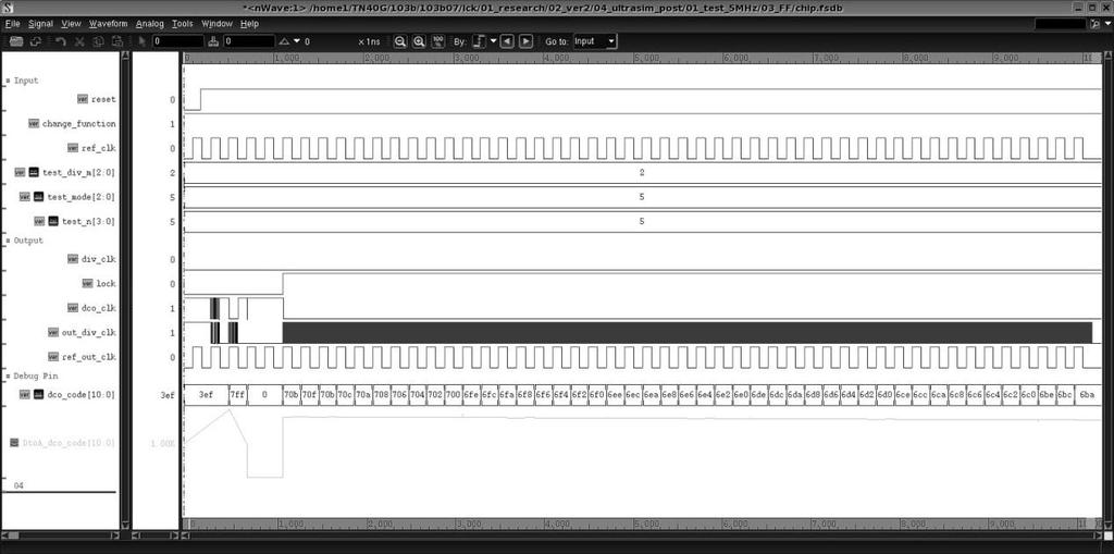
77 4.2 Simulation Results Test Mode Simulation The post-layout simulation result of the proposed ADPLL in various test modes is shown in Fig The dco_clk or the div_clk are blocked in different test modes. In addition, the div_clk is operated at test modes 1 to 3; the dco_clk is operated at test modes 4 to 7. The detail functions of each mode are shown in table 4.2. Therefore, as we measure the clock signals, the clock signals may not be interfered by each other. Fig. 4.3: System Simulation of the proposed ADPLL with various test modes. In Fig. 4.4(a), Fig. 4.4(b) and Fig. 4.4(c), we simulate the proposed ADPLL in TT corner, FF corner and SS corner, respectively. We set the test mode at 1 so that the dco_clk is disable output. The proposed fast lock-in ADPLL can lock correctly in different corner simulation

78 (a) (b)
國立交通大學 電子研究所 碩士論文 多電荷幫浦系統及可切換級數負電壓產生器之設計及生醫晶片應用
 國立交通大學 電子研究所 碩士論文 多電荷幫浦系統及可切換級數負電壓產生器之設計及生醫晶片應用 Design of Multiple-Charge-Pump System and Stage-Selective Negative Voltage Generator for Biomedical Applications 研究生 : 林曉平 (Shiau-Pin Lin) 指導教授 : 柯明道教授 (Prof.
A fast lock-in all-digital phase-locked loop in 40-nm CMOS technology
 LETTER IEICE Electronics Express, Vol.13, No.17, 1 10 A fast lock-in all-digital phase-locked loop in 40-nm CMOS technology Ching-Che Chung a) and Chi-Kuang Lo Department of Computer Science & Information
MULTILAYER HIGH CURRENT/HIGH FREQUENCY FERRITE CHIP BEAD
 INTRODUCTION 產品介紹 Multilayer high current chip beads are SMD components that possess a low DC resistance. Their impedance mainly comprises resistive part. Therefore, when this component is inserted in
PHASE-LOCKED loops (PLLs) are widely used in many
 are widely used in many") IEEE TRANSACTIONS ON CIRCUITS AND SYSTEMS II: EXPRESS BRIEFS, VOL. 58, NO. 3, MARCH 2011 149 Built-in Self-Calibration Circuit for Monotonic Digitally Controlled Oscillator Design in 65-nm CMOS Technology
IEEE TRANSACTIONS ON CIRCUITS AND SYSTEMS II: EXPRESS BRIEFS, VOL. 58, NO. 3, MARCH 2011 149 Built-in Self-Calibration Circuit for Monotonic Digitally Controlled Oscillator Design in 65-nm CMOS Technology
行政院國家科學委員會專題研究計畫成果報告
 行政院國家科學委員會專題研究計畫成果報告 W-CDMA 基地台接收系統之初始擷取與多用戶偵測子系統之研究與實作 Study and Implementation of the Acquisition and Multiuser Detection Subsystem for W-CDMA systems 計畫編號 :NSC 90-229-E-009-0 執行期限 : 90 年 月 日至 9 年 7
A GHz Wideband Sub-harmonically Injection- Locked PLL with Adaptive Injection Timing Alignment Technique
 A 2.4 3.6-GHz Wideband Sub-harmonically Injection- Locked PLL with Adaptive Injection Timing Alignment Technique Abstract: This paper proposes a wideband sub harmonically injection-locked PLL (SILPLL)
/$ IEEE
 IEEE TRANSACTIONS ON CIRCUITS AND SYSTEMS II: EXPRESS BRIEFS, VOL. 53, NO. 11, NOVEMBER 2006 1205 A Low-Phase Noise, Anti-Harmonic Programmable DLL Frequency Multiplier With Period Error Compensation for
微奈米光電製程 管傑雄 國立台灣大學電機系
 微奈米光電製程 管傑雄 國立台灣大學電機系 1 Outlines 1. 基本概念 2. Optical Lithography 3. E-Beam Lithography 4. Etching Techniques 5. Applications 6. Summary 2 基本概念 (I) Scattering Length 載子傳導並遭遇散射 1. 影響散射機制 : 雜質 ( 低溫 ) 及聲子振動
IN RECENT years, the phase-locked loop (PLL) has been a
 has been a") 430 IEEE TRANSACTIONS ON CIRCUITS AND SYSTEMS II: EXPRESS BRIEFS, VOL. 57, NO. 6, JUNE 2010 A Two-Cycle Lock-In Time ADPLL Design Based on a Frequency Estimation Algorithm Chia-Tsun Wu, Wen-Chung Shen,
430 IEEE TRANSACTIONS ON CIRCUITS AND SYSTEMS II: EXPRESS BRIEFS, VOL. 57, NO. 6, JUNE 2010 A Two-Cycle Lock-In Time ADPLL Design Based on a Frequency Estimation Algorithm Chia-Tsun Wu, Wen-Chung Shen,
書報討論報告 應用雙感測觸覺感測器於手術系統 之接觸力感測
 書報討論報告 應用雙感測觸覺感測器於手術系統 之接觸力感測 報告者 : 洪瑩儒 授課老師 : 劉雲輝教授 指導老師 : 莊承鑫 盧登茂教授 Department of Mechanical Engineering & Institute of Nanotechnology, Southern Taiwan University of Science and Technology, Tainan, TAIWAN
DESIGN OF MULTIPLYING DELAY LOCKED LOOP FOR DIFFERENT MULTIPLYING FACTORS
 DESIGN OF MULTIPLYING DELAY LOCKED LOOP FOR DIFFERENT MULTIPLYING FACTORS Aman Chaudhary, Md. Imtiyaz Chowdhary, Rajib Kar Department of Electronics and Communication Engg. National Institute of Technology,
Dedication. To Mum and Dad
 Dedication To Mum and Dad Acknowledgment Table of Contents List of Tables List of Figures A B A B 0 1 B A List of Abbreviations Abstract Chapter1 1 Introduction 1.1. Motivation Figure 1. 1 The relative
電機驅動方案產品介紹 廣閎科技 2016 May. 25 inergy 大比特研讨会资料区 :
 電機驅動方案產品介紹 廣閎科技 2016 May. 25 Copyright 2016 technology incorporation. All rights reserved. 廣閎科技簡介 廣閎科技是專注於節能方案應用之 IC 設計公司, 提供了由方案角度延伸的各類 IC 產品, 包含了照明 電源及電機驅動領域 廣閎科技不僅提供高品質的 IC 產品, 也協助客戶完成系統的設計及生產, 近幾年來更結合了許多上下游產業提供客戶更完整的服務
FPGA-based Stepping Motor Drive System Design
 基於 FPGA 的步進馬達驅動器設計 FPGA-based Stepping Motor Drive System Design 賴秋庚廖家宏戴勝淵林宏軒蔡守亮 Chiu-Keng Lai Chia-Hung Liao Sheng-Yuan Dai Hung-Hsuan Lin Chou-Liang ai 國立勤益科技大學電機工程系 Department of Electrical Engineering
Design of an Op-Amp Gain Compensator for Switched-Capacitor Integrators
 國立交通大學 電機與控制工程學系 碩士論文 交換電容式積分器 之運算放大器增益補償的設計 Design of an Op-mp Gain Compensator for Switched-Capacitor Integrators 研究生 : 許皓淵指導教授 : 鄭木火博士 中華民國九十七年七月 交換電容式積分器 之運算放大器增益補償的設計 Design of an Op-mp Gain Compensator
A Low-Power and Portable Spread Spectrum Clock Generator for SoC Applications
 IEEE TRANSACTIONS ON VERY LARGE SCALE INTEGRATION (VLSI) SYSTEMS 1 A Low-Power and Portable Spread Spectrum Clock Generator for SoC Applications Duo Sheng, Ching-Che Chung, and Chen-Yi Lee Abstract In
Delay-Locked Loop Using 4 Cell Delay Line with Extended Inverters
 International Journal of Electronics and Electrical Engineering Vol. 2, No. 4, December, 2014 Delay-Locked Loop Using 4 Cell Delay Line with Extended Inverters Jefferson A. Hora, Vincent Alan Heramiz,
CHAPTER 6 PHASE LOCKED LOOP ARCHITECTURE FOR ADC
 138 CHAPTER 6 PHASE LOCKED LOOP ARCHITECTURE FOR ADC 6.1 INTRODUCTION The Clock generator is a circuit that produces the timing or the clock signal for the operation in sequential circuits. The circuit
Acounter-basedall-digital spread-spectrum clock generatorwithhighemi reductionin65nmcmos
 LETTER IEICE Electronics Express, Vol.10, No.6, 1 6 Acounter-basedall-digital spread-spectrum clock generatorwithhighemi reductionin65nmcmos Ching-Che Chung 1a), Duo Sheng 2, and Wei-Da Ho 1 1 Department
凱思隆科技股份有限公司 公司與產品簡介. KeithLink Technology Co., Ltd. TEL: FAX:
 凱思隆科技股份有限公司 公司與產品簡介 KeithLink Technology Co., Ltd. TEL: 02-29786535 FAX: 02-29782726 service@keithlink.com 公司簡介 手動探針台 / 探針座 提供各式量測應用之探針台 / 探針座, 適用於 : 晶圓 ( 直流電性 或高頻 ) 量測 ; 液晶面板量測 ; 觸控面板 ITO 薄膜 導電高分子薄膜 矽晶片
Single-Stage Vernier Time-to-Digital Converter with Sub-Gate Delay Time Resolution
 Circuits and Systems, 2011, 2, 365-371 doi:10.4236/cs.2011.24050 Published Online October 2011 (http://www.scirp.org/journal/cs) Single-Stage Vernier Time-to-Digital Converter with Sub-Gate Delay Time
MODELING THE PHASE STEP RESPONSE OF BANG-BANG DIGITAL PLLS
 MODELING THE PHASE STEP RESPONSE OF BANG-BANG DIGITAL PLLS Moataz Abdelfattah Supervised by: AUC Prof. Yehea Ismail Dr. Maged Ghoniema Intel Dr. Mohamed Abdel-moneum (Industry Mentor) Outline Introduction
震波醫療機之設計與開發 Design and Development of Shock Wave Therapy
 震波醫療機之設計與開發 Design and Development of Shock Wave Therapy 梁勝明遠東科技大學電腦應用工程系教授 馬亞尼義守大學生物醫學工程學系副教授 1 萬龍瑞 國立成功大學航空太空學系研究生 摘 要 本研究設計與開發了一套具電子式高壓放電系統之電水式體外震波醫療機以提供在震波碎石術 骨疾治療 消脂及其他醫療技術所需之震波產生源 本文所設計與開發之震波醫療機是由五個子系統所組成,
Integrated Circuit Design for High-Speed Frequency Synthesis
 Integrated Circuit Design for High-Speed Frequency Synthesis John Rogers Calvin Plett Foster Dai ARTECH H O US E BOSTON LONDON artechhouse.com Preface XI CHAPTER 1 Introduction 1 1.1 Introduction to Frequency
A Frequency Synthesis of All Digital Phase Locked Loop
 A Frequency Synthesis of All Digital Phase Locked Loop S.Saravanakumar 1, N.Kirthika 2 M.E.VLSI DESIGN Sri Ramakrishna Engineering College Coimbatore, Tamilnadu 1 s.saravanakumar21@gmail.com, 2 kirthi.com@gmail.com
This chapter discusses the design issues related to the CDR architectures. The
 Chapter 2 Clock and Data Recovery Architectures 2.1 Principle of Operation This chapter discusses the design issues related to the CDR architectures. The bang-bang CDR architectures have recently found
Lecture 11: Clocking
 High Speed CMOS VLSI Design Lecture 11: Clocking (c) 1997 David Harris 1.0 Introduction We have seen that generating and distributing clocks with little skew is essential to high speed circuit design.
ALL-DIGITAL FREQUENCY SYNTHESIZER IN DEEP-SUBMICRON CMOS
 ALL-DIGITAL FREQUENCY SYNTHESIZER IN DEEP-SUBMICRON CMOS ROBERT BOGDAN STASZEWSKI Texas Instruments PORAS T. BALSARA University of Texas at Dallas WILEY- INTERSCIENCE A JOHN WILEY & SONS, INC., PUBLICATION
Wireless Communications
 Wireless Communications Chapter 2 Modern Wireless Communication Systems [1] The widespread adoption of wireless communications was accelerated in the mid 1990s, when governments throughout the world provided
Design of an Efficient Phase Frequency Detector for a Digital Phase Locked Loop
 Design of an Efficient Phase Frequency Detector for a Digital Phase Locked Loop Shaik. Yezazul Nishath School Of Electronics Engineering (SENSE) VIT University Chennai, India Abstract This paper outlines
Biju Viswanath Rajagopal P C Ramya Nair S R Jobin Cyriac. QuEST Global
 an effective design and verification methodology for digital PLL This Paper depicts an effective simulation methodology to overcome the spice simulation time overhead of digital dominant, low frequency
Taheri: A 4-4.8GHz Adaptive Bandwidth, Adaptive Jitter Phase Locked Loop
 Engineering, Technology & Applied Science Research Vol. 7, No. 2, 2017, 1473-1477 1473 A 4-4.8GHz Adaptive Bandwidth, Adaptive Jitter Phase Locked Loop Hamidreza Esmaeili Taheri Department of Electronics
Design of Pipeline Analog to Digital Converter
 Design of Pipeline Analog to Digital Converter Vivek Tripathi, Chandrajit Debnath, Rakesh Malik STMicroelectronics The pipeline analog-to-digital converter (ADC) architecture is the most popular topology
Power Challenges for IoT devices
 Power Challenges for IoT devices Wireless signaling test/ DC Power consumption Solution Architect/ Keysight General Electronic Measurement Soluiton R&D Brian Chi 祁子年 Agenda IOT Signaling Test Solution
國立交通大學 經營管理研究所 碩士論文 上游獨占下之外部授權者的最適授權策略. The Optimal Licensing Strategy of an Outsider Patentee under. the Single Upstream Supplier 研究生 : 林錦宏
 國立交通大學 經營管理研究所 碩士論文 上游獨占下之外部授權者的最適授權策略 The Optimal Licensing Strategy of an Outsider Patentee under the Single Upstream Supplier 研究生 : 林錦宏 指導教授 : 胡均立教授 中華民國九十八年五月 上游獨占下之外部授權者的最適授權策略 The Optimal Licensing
#5802 使用者研究 Design and Research on User Experience
 本週課程大綱 #5802 使用者研究 Design and Research on User Experience Week 02 交大應用藝術研究所 / 工業技術研究院資通所 Dr. 莊雅量 複習 : 使用者研究的趨勢與重要性 Chap 1. Experience in Products 相關調查方法概論 Chap 2. Inquiring about Pepole s Affective Product
Designing Nano Scale CMOS Adaptive PLL to Deal, Process Variability and Leakage Current for Better Circuit Performance
 International Journal of Innovative Research in Electronics and Communications (IJIREC) Volume 1, Issue 3, June 2014, PP 18-30 ISSN 2349-4042 (Print) & ISSN 2349-4050 (Online) www.arcjournals.org Designing
Case5:08-cv PSG Document Filed09/17/13 Page1 of 11 EXHIBIT
 Case5:08-cv-00877-PSG Document578-15 Filed09/17/13 Page1 of 11 EXHIBIT N ISSCC 2004 Case5:08-cv-00877-PSG / SESSION 26 / OPTICAL AND Document578-15 FAST I/O / 26.10 Filed09/17/13 Page2 of 11 26.10 A PVT
國立交通大學 電子工程學系電子研究所 碩士論文. An Effective Heart Rate Variability Processor Design for. Portable 3-Lead ECG Monitoring System-on-Chip 研究生 : 曾少彥
 國立交通大學 電子工程學系電子研究所 碩士論文 適用於可攜式三通道 ECG 遠端照護系統晶片之有 效的心跳變異率處理器設計 An Effective Heart Rate Variability Processor Design for Portable 3-Lead ECG Monitoring System-on-Chip 研究生 : 曾少彥 指導教授 : 方偉騏教授 中華民國九十九年十二月 適用於可攜式三通道
國立交通大學 碩士論文 90 奈米互補式金氧半製程下 之多功能輸入 / 輸出元件庫設計. Design of Configurable I/O Cell Library in 90-nm CMOS Process
 國立交通大學 電子工程學系 電子研究所碩士班 碩士論文 90 奈米互補式金氧半製程下 之多功能輸入 / 輸出元件庫設計 Design of Configurable I/O Cell Library in 90-nm CMOS Process 研究生 : 陳世範 (Shih-Fan Chen) 指導教授 : 柯明道教授 (Prof. Ming-Dou Ker) 中華民國九十七年九月 90 奈米互補式金氧半製程下
國立交通大學 資訊科學與工程研究所碩士論文 多天線傳送系統干擾抑制及路徑衰減補償之可適性封包檢測. Adaptive Packet Acquisition with Interference and Time-Variant Path Loss in MIMO-OFDM Systems
 國立交通大學 資訊科學與工程研究所碩士論文 多天線傳送系統干擾抑制及路徑衰減補償之可適性封包檢測 Adaptive Packet Acquisition with Interference and Time-Variant Path Loss in MIMO-OFDM Systems 研究生 : 呂理聖 指導教授 : 許騰尹教授 中華民國九十五年七月 多天線傳送系統干擾抑制及路徑衰減補償之可適性封包檢測
24GHz BSD Radar. 24 GHz Radar Blind Spot Detection. Installation Guide
 P/N : VS-91A001 Page :1 of 8 24 GHz Radar Blind Spot Detection Installation Guide P/N : VS-91A001 Page :2 of 8 CONTENT 1. SYSTEM ARCHITECTURE TURE 1.1 Layout... 3 1.2 Components.....4 2. Installation 2.1
FACTORS INFLUENCING THE ADOPTION OF LEAN MANUFACTURING: EVIDENCE FROM A CHINESE MANUFACTURING FIRM
 FACTORS INFLUENCING THE ADOPTION OF LEAN MANUFACTURING: EVIDENCE FROM A CHINESE MANUFACTURING FIRM SIU KWOK HUNG DOCTOR OF BUSINESS ADMINISTRATION CITY UNIVERSITY OF HONG KONG JULY 2014 CITY UNIVERSITY
A wide-range all-digital duty-cycle corrector with output clock phase alignment in 65 nm CMOS technology
 A wide-range all-digital duty-cycle corrector with output clock phase alignment in 65 nm CMOS technology Ching-Che Chung 1a), Duo Sheng 2, and Sung-En Shen 1 1 Department of Computer Science & Information
NT-8540 / NT-8560 / NT-8580 Laser Distance Measurer
 NT-8540 / NT-8560 / NT-8580 Laser Distance Measurer User s Manual 1 st Edition, 2015 2015 Prokit s Industries Co., Ltd Overview Please carefully read this product Quick Start to ensure the safe and efficient
Publication Lists (2001~2005) 1. Journal Papers:
 1. Journal Papers:") Liaw, Chang-Ming ( 廖聰明 ) Professor Ph.D., National Tsing Hua University, 1988 Power Electronics, Motor Drive, Electric Machine Control E-mail: cmliaw@ee.nthu.edu.tw Fax: 886-3-5715971 Dr. Liaw was born
Liaw, Chang-Ming ( 廖聰明 ) Professor Ph.D., National Tsing Hua University, 1988 Power Electronics, Motor Drive, Electric Machine Control E-mail: cmliaw@ee.nthu.edu.tw Fax: 886-3-5715971 Dr. Liaw was born
Power Efficient Digital LDO Regulator with Transient Response Boost Technique K.K.Sree Janani 1, M.Balasubramani 2
 Power Efficient Digital LDO Regulator with Transient Response Boost Technique K.K.Sree Janani 1, M.Balasubramani 2 1 PG student, Department of ECE, Vivekanandha College of Engineering for Women. 2 Assistant
Unit 6: Movies. Film Genre ( 可加 film 或 movie) Adjectives. Vocabulary. animation. action. drama. comedy. crime. romance. horror
 Adjectives. Vocabulary. animation. action. drama. comedy. crime. romance. horror") Unit 6: Movies Vocabulary Film Genre ( 可加 film 或 movie) action comedy romance horror thriller adventure animation drama crime science fiction (sci-fi) musical war Adjectives exciting fascinating terrifying
Unit 6: Movies Vocabulary Film Genre ( 可加 film 或 movie) action comedy romance horror thriller adventure animation drama crime science fiction (sci-fi) musical war Adjectives exciting fascinating terrifying
INNOVATIVE PASSIVE MICROWAVE COMPONENTS FOR WIRELESS COMMUNICATION
 INNOVATIVE PASSIVE MICROWAVE COMPONENTS FOR WIRELESS COMMUNICATION CHEUNG KING YIN MASTER OF PHILOSOPHY CITY UNIVERSITY OF HONG KONG SEPTEMBER 2010 CITY UNIVERSITY OF HONG KONG 香港城市大學 Innovative Passive
海象觀測同調性都卜勒微波雷達的開發 林昭暉 國立中央大學水文與海洋科學研究所助理教授 2 國立中央大學水文與海洋科學研究所博士班研究生 2 國立中央大學水文與海洋科學研究所研究助理 國家實驗研究院台灣海洋科技研究中心助理研究員
 第 35 屆海洋工程研討會論文集國立中山大學 2013 年 11 月 Proceedings of the 35 th Ocean Engineering Conference in Taiwan National Sun Yat-sen University, November 2013 海象觀測同調性都卜勒微波雷達的開發 錢樺 1 鄭皓元 2 林昭暉 3 賴堅戊 1 國立中央大學水文與海洋科學研究所助理教授
Multiple Reference Clock Generator
 A White Paper Presented by IPextreme Multiple Reference Clock Generator Digitial IP for Clock Synthesis August 2007 IPextreme, Inc. This paper explains the concept behind the Multiple Reference Clock Generator
Fast-lock all-digital DLL and digitally-controlled phase shifter for DDR controller applications
 Fast-lock all-digital DLL and digitally-controlled phase shifter for DDR controller applications Duo Sheng 1a), Ching-Che Chung 2,andChen-YiLee 1 1 Department of Electronics Engineering & Institute of
A Compact, Low-Power Low- Jitter Digital PLL. Amr Fahim Qualcomm, Inc.
 A Compact, Low-Power Low- Jitter Digital PLL Amr Fahim Qualcomm, Inc. 1 Outline Introduction & Motivation Digital PLL Architectures Proposed DPLL Architecture Analysis of DPLL DPLL Adaptive Algorithm DPLL
Fractional- N PLL with 90 Phase Shift Lock and Active Switched- Capacitor Loop Filter
 J. Park, F. Maloberti: "Fractional-N PLL with 90 Phase Shift Lock and Active Switched-Capacitor Loop Filter"; Proc. of the IEEE Custom Integrated Circuits Conference, CICC 2005, San Josè, 21 September
可程式計數陣列 (PCA) 功能使用方法. 可程式計數陣列功能使用方法 Application Note 1 適用產品 :SM59D04G2,SM59D03G2
 功能使用方法. 可程式計數陣列功能使用方法 Application Note 1 適用產品 :SM59D04G2,SM59D03G2") 可程式計數陣列 (PCA) 功能使用方法 1 適用產品 :SM59D04G2,SM59D03G2 2 應用說明 : PCA 共有五組, 每組皆可工作於以下七種模式 : 捕獲模式 - 正緣捕獲模式 (Positive edge capture mode) 捕獲模式 - 負緣捕獲模式 (Negative edge capture mode) 捕獲模式 - 正緣及負緣捕獲模式 (Both positive
可程式計數陣列 (PCA) 功能使用方法 1 適用產品 :SM59D04G2,SM59D03G2 2 應用說明 : PCA 共有五組, 每組皆可工作於以下七種模式 : 捕獲模式 - 正緣捕獲模式 (Positive edge capture mode) 捕獲模式 - 負緣捕獲模式 (Negative edge capture mode) 捕獲模式 - 正緣及負緣捕獲模式 (Both positive
A Fast-Transient Wide-Voltage-Range Digital- Controlled Buck Converter with Cycle- Controlled DPWM
 A Fast-Transient Wide-Voltage-Range Digital- Controlled Buck Converter with Cycle- Controlled DPWM Abstract: This paper presents a wide-voltage-range, fast-transient all-digital buck converter using a
國立交通大學 工業工程與管理學系 博士論文 利用電腦輔助設計資料防止錯打線的視覺偵測系統之設計與開發
 國立交通大學 工業工程與管理學系 博士論文 利用電腦輔助設計資料防止錯打線的視覺偵測系統之設計與開發 A CAD-based Vision Approach for Incorrect Wire Bonding Prevention System Design and Development 研究生:李恕明 指導教授:彭德保博士 中華民國九十八年七月 利用電腦輔助設計資料防止錯打線的視覺偵測系統之設計
國立交通大學 材料科學與工程學研究所 碩士論文
 國立交通大學 材料科學與工程學研究所 碩士論文 使用 I-line 步進機與電子束微影並應用在 MHEMT 元件的新穎 T- 形閘極製作方法之研究 Study of Novel T-gate Fabrication Methods Using I-line Stepper and Electron Beam System with Application to MHEMT Devices 研究生 :
Modeling And Implementation of All-Digital Phase-Locked Loop Based on Vernier Gated Ring Oscillator Time-to-Digital Converter
 Master s Thesis Modeling And Implementation of All-Digital Phase-Locked Loop Based on Vernier Gated Ring Oscillator Time-to-Digital Converter Ji Wang Department of Electrical and Information Technology,
數位示波器原理準確量測與除錯技巧. 浩網科技股份有限公司應用工程暨高速數位測試中心 - 處長賴德謙 (Ted Lai ) 2014 INFINET TECHNOLOGY
 2014 INFINET TECHNOLOGY") 數位示波器原理準確量測與除錯技巧 浩網科技股份有限公司應用工程暨高速數位測試中心 - 處長賴德謙 (Ted Lai ) 1 2014 INFINET TECHNOLOGY Agenda 異常波型範例, Ghostly Waveform Examples 示波器當為抓鬼特攻隊的重要特性 : 頻寬 & 採樣率 記憶體儲存深度 波形更新率 示波器實際量測操作技巧 進階的參數觸發設定條件 針對不常出現的事件執行觸發
數位示波器原理準確量測與除錯技巧 浩網科技股份有限公司應用工程暨高速數位測試中心 - 處長賴德謙 (Ted Lai ) 1 2014 INFINET TECHNOLOGY Agenda 異常波型範例, Ghostly Waveform Examples 示波器當為抓鬼特攻隊的重要特性 : 頻寬 & 採樣率 記憶體儲存深度 波形更新率 示波器實際量測操作技巧 進階的參數觸發設定條件 針對不常出現的事件執行觸發
國立交通大學 碩士論文. Design and Realization of Capacitive Sensor Readout Circuit in LTPS Technology 研究生 : 林佑達. (Yu-Ta Lin) 指導教授 : 柯明道教授 (Prof.
 指導教授 : 柯明道教授 (Prof.") 國立交通大學 電子工程學系 電子研究所碩士班 碩士論文 應用於低溫多晶矽製程下電容式感測器電容式感測器讀出讀出電路設計與實現 Design and Realization of Capacitive Sensor Readout Circuit in LTPS Technology 研究生 : 林佑達 (Yu-Ta Lin) 指導教授 : 柯明道教授 (Prof. Ming-Dou Ker) 中華民國九十九年九月
國立交通大學 電子工程學系 電子研究所碩士班 碩士論文 應用於低溫多晶矽製程下電容式感測器電容式感測器讀出讀出電路設計與實現 Design and Realization of Capacitive Sensor Readout Circuit in LTPS Technology 研究生 : 林佑達 (Yu-Ta Lin) 指導教授 : 柯明道教授 (Prof. Ming-Dou Ker) 中華民國九十九年九月
User s Manual. Wi-Fi Smart Plug HS100 Wi-Fi Smart Plug with Energy Monitoring HS REV 2.0.0
 Wi-Fi Smart Plug HS100 Wi-Fi Smart Plug with Energy Monitoring HS110 1910012024 REV 2.0.0 Copyright & Trademarks Specifications are subject to change without notice. TP-Link is a registered trademark of
OEM Installation Guidance Document For BRCM WLAN + Bluetooth Module, BCM94313HMGB FCC ID: QDS-BRCM1051; IC: 4324A-BRCM1051
 Conditions on using BRCM regulatory approvals: A. Customer must ensure that its product (the CUSTOMER Product ) is electrically identical to Broadcom s reference designs. Customer acknowledges that any
Chapter 3 Novel Digital-to-Analog Converter with Gamma Correction for On-Panel Data Driver
 Chapter 3 Novel Digital-to-Analog Converter with Gamma Correction for On-Panel Data Driver 3.1 INTRODUCTION As last chapter description, we know that there is a nonlinearity relationship between luminance
Multi-bit Sigma-Delta TDC Architecture for Digital Signal Timing Measurement
 IEEE International ixed-signals, Sensors, and Systems Test Workshop, Taipei, 22 ulti-bit Sigma-Delta TDC Architecture for Digital Signal Timing easurement S. emori,. Ishii, H. Kobayashi, O. Kobayashi T.
Lecture 7: Components of Phase Locked Loop (PLL)
") Lecture 7: Components of Phase Locked Loop (PLL) CSCE 6933/5933 Instructor: Saraju P. Mohanty, Ph. D. NOTE: The figures, text etc included in slides are borrowed from various books, websites, authors pages,
Lecture 7: Components of Phase Locked Loop (PLL) CSCE 6933/5933 Instructor: Saraju P. Mohanty, Ph. D. NOTE: The figures, text etc included in slides are borrowed from various books, websites, authors pages,
AS THE DATA rate demanded by multimedia system
 424 IEEE TRANSACTIONS ON CIRCUITS AND SYSTEMS II: EXPRESS BRIEFS, VOL. 59, NO. 7, JULY 2012 An All-Digital Large-N Audio Frequency Synthesizer for HDMI Applications Ching-Che Chung, Member, IEEE, Duo Sheng,
Design of Low Noise 16-bit CMOS Digitally Controlled Oscillator
 Design of Low Noise 16-bit CMOS Digitally Controlled Oscillator Nitin Kumar #1, Manoj Kumar *2 # Ganga Institute of Technology & Management 1 nitinkumarvlsi@gmail.com * Guru Jambheshwar University of Science
A fast programmable frequency divider with a wide dividing-ratio range and 50% duty-cycle
 A fast programmable frequency divider with a wide dividing-ratio range and 50% duty-cycle Mo Zhang a), Syed Kamrul Islam b), and M. Rafiqul Haider c) Department of Electrical & Computer Engineering, University
A Flying-Adder Architecture of Frequency and Phase Synthesis With Scalability
 IEEE TRANSACTIONS ON VERY LARGE SCALE INTEGRATION (VLSI) SYSTEMS, VOL. 10, NO. 5, OCTOBER 2002 637 A Flying-Adder Architecture of Frequency and Phase Synthesis With Scalability Liming Xiu, Member, IEEE,
FPGA IMPLEMENTATION OF POWER EFFICIENT ALL DIGITAL PHASE LOCKED LOOP
 INTERNATIONAL JOURNAL OF ELECTRONICS AND COMMUNICATION ENGINEERING & TECHNOLOGY (IJECET) Proceedings of the International Conference on Emerging Trends in Engineering and Management (ICETEM14) ISSN 0976
The Electronic Design Automation (EDA) Lab
 Lab") The Electronic Design Automation (EDA) Lab 張耀文 Yao-Wen Chang ywchang@cc.ee.ntu.edu.tw http://cc.ee.ntu.edu.tw/~ywchang Graduate Institute of Electronics Engineering Department of Electrical Engineering
The Electronic Design Automation (EDA) Lab 張耀文 Yao-Wen Chang ywchang@cc.ee.ntu.edu.tw http://cc.ee.ntu.edu.tw/~ywchang Graduate Institute of Electronics Engineering Department of Electrical Engineering
DOUBLE DATA RATE (DDR) technology is one solution
 technology is one solution") 54 IEEE TRANSACTIONS ON VERY LARGE SCALE INTEGRATION (VLSI) SYSTEMS, VOL. 2, NO. 6, JUNE 203 All-Digital Fast-Locking Pulsewidth-Control Circuit With Programmable Duty Cycle Jun-Ren Su, Te-Wen Liao, Student
54 IEEE TRANSACTIONS ON VERY LARGE SCALE INTEGRATION (VLSI) SYSTEMS, VOL. 2, NO. 6, JUNE 203 All-Digital Fast-Locking Pulsewidth-Control Circuit With Programmable Duty Cycle Jun-Ren Su, Te-Wen Liao, Student
ALTHOUGH zero-if and low-if architectures have been
 IEEE JOURNAL OF SOLID-STATE CIRCUITS, VOL. 40, NO. 6, JUNE 2005 1249 A 110-MHz 84-dB CMOS Programmable Gain Amplifier With Integrated RSSI Function Chun-Pang Wu and Hen-Wai Tsao Abstract This paper describes
Low Power Design of Successive Approximation Registers
 Low Power Design of Successive Approximation Registers Rabeeh Majidi ECE Department, Worcester Polytechnic Institute, Worcester MA USA rabeehm@ece.wpi.edu Abstract: This paper presents low power design
射頻微波通訊電路設計 RF/Microwave Communication Circuits Design
 射頻微波通訊電路設計 RF/Microwave Communication Circuits Design Huey-Ru Chuang CCE/EE NCKU 莊惠如成功大學電通所 / 電機工程系 2014 Interference signals Desired Channel c Interference signals BPF response Desired Channel c LNA SHM
Digital Dual Mixer Time Difference for Sub-Nanosecond Time Synchronization in Ethernet
 Digital Dual Mixer Time Difference for Sub-Nanosecond Time Synchronization in Ethernet Pedro Moreira University College London London, United Kingdom pmoreira@ee.ucl.ac.uk Pablo Alvarez pablo.alvarez@cern.ch
Multimeter 3 1/2經濟款數位電錶 MT User s Manual 2nd Edition, Copyright by Prokit s Industries Co., Ltd.
 MT-1210 Multimeter 3 1/2經濟款數位電錶 User s Manual 2nd Edition, 2017 2017 Copyright by Prokit s Industries Co., Ltd. SAFETY INFORMATION This multimeter has been designed according to IEC 1010 concerning electronic
A Monotonic and Low-Power Digitally Controlled Oscillator Using Standard Cells for SoC Applications
 A Monotonic and Low-Power Digitally Controlled Oscillator Using Standard Cells for SoC Applications Duo Sheng, Ching-Che Chung, and Jhih-Ci Lan Department of Electrical Engineering, Fu Jen Catholic University,
計畫編號 : NSC E 執行時程 : 93 年 8 月 1 日至 94 年 7 月 31 日 計畫主持人 : 連豊力 國立台灣大學電機系助理教授 共同主持人 : 呂良鴻 國立台灣大學電子所助理教授 計畫參與人員 : 許瑋豪 方文杰 林雍倫 馮天俊 魏嘉樑 麥肇元
 微型仿生生物體之研發 (2/3) 子計畫二 : 生物群體協調行為之探討與無線通訊機制之整合 (2/3) Study of Group Behaviors of Biological Systems and Integration of Wireless Communication Protocol Design 計畫編號 : NSC 93-2213-E-002-049- 執行時程 : 93 年 8
A Fast Locking Digital Phase-Locked Loop using Frequency Difference Stage
 International Journal of Engineering & Technology IJET-IJENS Vol:14 No:04 75 A Fast Locking Digital Phase-Locked Loop using Frequency Difference Stage Mohamed A. Ahmed, Heba A. Shawkey, Hamed A. Elsemary,
Sudatta Mohanty, Madhusmita Panda, Dr Ashis kumar Mal
 International Journal of Scientific & Engineering Research, Volume 5, Issue 5, May-2014 45 Design and Performance Analysis of a Phase Locked Loop using Differential Voltage Controlled Oscillator Sudatta
A 10-Gb/s Multiphase Clock and Data Recovery Circuit with a Rotational Bang-Bang Phase Detector
 JOURNAL OF SEMICONDUCTOR TECHNOLOGY AND SCIENCE, VOL.16, NO.3, JUNE, 2016 ISSN(Print) 1598-1657 http://dx.doi.org/10.5573/jsts.2016.16.3.287 ISSN(Online) 2233-4866 A 10-Gb/s Multiphase Clock and Data Recovery
Enhancing FPGA-based Systems with Programmable Oscillators
 Enhancing FPGA-based Systems with Programmable Oscillators Jehangir Parvereshi, jparvereshi@sitime.com Sassan Tabatabaei, stabatabaei@sitime.com SiTime Corporation www.sitime.com 990 Almanor Ave., Sunnyvale,
國立交通大學 電信工程學系 碩士論文 連續時間轉導電容式三角積分調變器之實現. Implementation of the continuous-time transconductor-capacitor Delta-Sigma modulator 研究生 : 吳國璽 指導教授 : 洪崇智博士
 國立交通大學 電信工程學系 碩士論文 連續時間轉導電容式三角積分調變器之實現 Implementation of the continuous-time transconductor-capacitor Delta-Sigma modulator 研究生 : 吳國璽 指導教授 : 洪崇智博士 中華民國九十六年十月 連續時間轉導電容式三角積分調變器之實現 Implementation of the continuous-time
PIR Detector. 1. Introduction. 2. Principle of PIR detector
 PIR Detector 5F., No.172, Sec. 4, Chengde Rd., Shilin Dist., Taipei City 11167, Taiwan 1. Introduction In recent years, as greenhouse effect brings about global climate abnormality, all products are designed
5G Technology Development in ITRI
 5G Technology Development in ITRI Pang-An Ting Division for Emerging Wireless Application Technology ICL/ITRI 2017/01/22 Copyright 2017 ITRI 工業技術研究院 Our Views on 5G R&D Copyright 2017 ITRI 工業技術研究院 3 Our
Transient Response Boosted D-LDO Regulator Using Starved Inverter Based VTC
 Research Manuscript Title Transient Response Boosted D-LDO Regulator Using Starved Inverter Based VTC K.K.Sree Janani, M.Balasubramani P.G. Scholar, VLSI Design, Assistant professor, Department of ECE,
Using the Keyboard (VGP-WKB11)
") n 32 (VGP-WKB11) A wireless keyboard is supplied with your computer. The wireless keyboard uses a standard key arrangement with additional keys that perform specific functions. Using the Wireless Keyboard
n 32 (VGP-WKB11) A wireless keyboard is supplied with your computer. The wireless keyboard uses a standard key arrangement with additional keys that perform specific functions. Using the Wireless Keyboard
A Phase-Locked Loop with Embedded Analog-to-Digital Converter for Digital Control
 A Phase-Locked Loop with Embedded Analog-to-Digital Converter for Digital Control Sooho Cha, Chunseok Jeong, and Changsik Yoo A phase-locked loop (PLL) is described which is operable from 0.4 GHz to 1.2
DBUB-P705 Bluetooth Adapter User s Manual
 DBUB-P705 Bluetooth Adapter User s Manual This document provides safety instructions and describes the specifications. Read this document carefully before installing to ensure your safety and product performance.
ANALOG-TO-DIGITAL CONVERTER FOR INPUT VOLTAGE MEASUREMENTS IN LOW- POWER DIGITALLY CONTROLLED SWITCH-MODE POWER SUPPLY CONVERTERS
 ANALOG-TO-DIGITAL CONVERTER FOR INPUT VOLTAGE MEASUREMENTS IN LOW- POWER DIGITALLY CONTROLLED SWITCH-MODE POWER SUPPLY CONVERTERS Aleksandar Radić, S. M. Ahsanuzzaman, Amir Parayandeh, and Aleksandar Prodić
Lecture 160 Examples of CDR Circuits in CMOS (09/04/03) Page 160-1
 Page 160-1") Lecture 160 Examples of CDR Circuits in CMOS (09/04/03) Page 160-1 LECTURE 160 CDR EXAMPLES INTRODUCTION Objective The objective of this presentation is: 1.) Show two examples of clock and data recovery
Lecture 160 Examples of CDR Circuits in CMOS (09/04/03) Page 160-1 LECTURE 160 CDR EXAMPLES INTRODUCTION Objective The objective of this presentation is: 1.) Show two examples of clock and data recovery
CHAPTER. delta-sigma modulators 1.0
 CHAPTER 1 CHAPTER Conventional delta-sigma modulators 1.0 This Chapter presents the traditional first- and second-order DSM. The main sources for non-ideal operation are described together with some commonly
A VCO-based analog-to-digital converter with secondorder sigma-delta noise shaping
 A VCO-based analog-to-digital converter with secondorder sigma-delta noise shaping The MIT Faculty has made this article openly available. Please share how this access benefits you. Your story matters.
A Wide-Bandwidth 2.4GHz ISM Band Fractional-N PLL with Adaptive Phase Noise Cancellation. Outline
 A Wide-Bandwidth 2.4GHz ISM Band Fractional-N PLL with Adaptive Phase Noise Cancellation Ashok Swaminathan,2, Kevin J. Wang, Ian Galton University of California, San Diego, CA 2 NextWave Broadband, San
Design of Phase Locked Loop as a Frequency Synthesizer Muttappa 1 Akalpita L Kulkarni 2
 IJSRD - International Journal for Scientific Research & Development Vol. 3, Issue 03, 2015 ISSN (online): 2321-0613 Design of Phase Locked Loop as a Frequency Synthesizer Muttappa 1 Akalpita L Kulkarni
All Digital Phase Locked Loop Architecture Design Using Vernier Delay Time-to- Digital Converter
 ISSN:1991-8178 Australian Journal of Basic and Applied Sciences Journal home page: www.ajbasweb.com All Digital Phase Locked Loop Architecture Design Using Vernier Delay Time-to- Digital Converter 1 T.M.
CHAPTER III THE FPGA IMPLEMENTATION OF PULSE WIDTH MODULATION
 34 CHAPTER III THE FPGA IMPLEMENTATION OF PULSE WIDTH MODULATION 3.1 Introduction A number of PWM schemes are used to obtain variable voltage and frequency supply. The Pulse width of PWM pulsevaries with