SEM Magnification Calibration & Verification: Building Confidence in Your Scale Bar
|
|
|
- Amanda Paul
- 5 years ago
- Views:
Transcription

1 SEM Magnification Calibration & Verification: Building Confidence in Your Scale Bar Mark A. Koten, Ph.D. Senior Research Scientist Electron Optics Group McCrone Associates

2 Why check your SEM image calibration? Everyone should want to ensure the scale bar on the image is accurate The initial magnification calibration may not have been as rigorous as you think Serious maintenance on your SEM may have altered the magnification calibration Who checks this? Microscope specialists/supervisors/managers Eperienced users It may be required on a routine basis Industrial labs that have ISO or similar accreditation requirements SEM Magnification Calibration 2
.")
3 SEM Magnification Definition The ratio of a length measured on the SEM monitor (L m ) to the same length measured on the sample (L s ). M = L m L s The length measured could be anything as long as they are equivalent. How does the SEM change magnification? Scan coils change the scan length (L s ). SEM Magnification Calibration 3
4 Magnification Eamples Eample 1 HFOV Eample 2 Piel Magnification Image width Scan length Image piel size Scan piel size (M) (L m1 ) (L s1 ) (L m2 ) (L s2 ) cm mm 190 um 19.0 um cm 2.40 mm 190 um 1.9 um 1, cm 0.24 mm 190 um 0.2 um 10, cm um 190 um 19.0 nm 100, cm 2.40 um 190 um 1.9 nm 1,000, cm 0.24 um 190 um 0.2 nm Monitor Image piels m M = L m L s Problem: beam diameters range from 1 nm 1 um SEM Magnification Calibration 4
5 Digital Resolution vs Imaging Resolution How large is your beam s probe size? How large is your beam s interaction volume? What is the beam s shape? -Interaction volume depends on voltage -Gaussian curve with FWHM Probe size Electron Beam Electron Beam How large are the piels in your image? What distance does the beam travel between two piels? -Piel sizes range from 0.2 nm to 20 um! At higher magnifications the digital resolution can vastly eceed the instrument resolution. SEM Magnification Calibration 5
6 SEM Image Formation Where s the ray diagram? Different from image projection cameras found in optical imaging and bright field TEM applications The beam is controlled very precisely by a scan generator, which deflects the beam over the sample in a grid pattern The detector collects electrons (SE or BSE) for each beam position (, y)-space and saves the number of electrons detected (intensity) at that location. The computer then maps this information into a file with a readable format (tiff, png, jpeg, ) that can display the electron intensity measured on a computer screen as a digital image. Beam Locations Saturation Intensity Grayscale SEM image.tiff -Intensity range corresponds to grayscale values -Contrast is amplitude -Brightness is offset Specimen Detector Zero signal SEM Magnification Calibration 6
7 What is actually being calibrated? The distance the beam moves in both the and y direction The beam positions will be mapped to a square grid (piels are squares) Distortions in the image can arise if the travel distance is not equal in both and y directions If the distances between piels is unknown or inaccurate then measurements will be wrong Specimen Specimen SEM Magnification Calibration 7


8 The Nominal Magnification Parado L m3 Magnification changes from screen to screen L m1 L m2 M = L m L s L m1 L m2 L m3 M 1 M 2 M 3 Scale bars solve this problem by placing a measurement of L s inside the image! SEM Magnification Calibration 8

9 Nominal Magnification vs Scale Bar Nominal Magnification Only No value of L s is saved L m changes depending on the screen you are using (can always measure this) The saved magnification is no longer valid unless you are on the microscope PC Features in your image can t be measured at a later date on different PC If you want to measure something, you have to go back to the microscope PC Scale Bar A value of L s travels with the image in the scale bar L m changes depending on the screen you are using (can always measure this) For different screens you can find your actual magnification Can make measurements of sample features at a later date on any PC Another person can more easily interpret the sizes of the features in the image SEM Magnification Calibration 9


10 Making Measurements from Calibrated Images Advance image analysis often done on third party software such as imagej or image-pro can be used to make precise and comple measurements of your samples These measurements often require distance unit dimensions rather than piels This requires a conversion factor of piels to micrometers/nanometers Your scale bar can be used within imagej to obtain this pi/nm ratio Just measure the length of your scale bar in piels and divide that by its length in dimensional units There is usually a set scale function that allows for the software to apply this ratio to the image or image stack SEM Magnification Calibration 10


11 What features make a good calibration tool? Chemically and structurally stable Sharp edges that don t use a lot of piels Something periodic spanning ~4 orders of magnitude (100 nm to 1 mm) Pitch doesn t deviate too much from the mean at any point Pitch is constant over a wide range of length scales Some things to avoid using for calibration or verification: SEM Magnification Calibration 11
 United States: NIST www.nist.")
 Germany: PTB (Physikalisch-Technische Bundesanstalt) An SRM that is traceable back to an NMI like NIST Unbroken chain")

12 What Standard Reference Material Should You Use? Best sources for SRMs are National Metrological Institutes (NMI) United States: NIST United Kingdom: NPL (National Physical Laboratory) France: LNE (Laboratoire National d'essais) Germany: PTB (Physikalisch-Technische Bundesanstalt) An SRM that is traceable back to an NMI like NIST Unbroken chain of validation from processing to measurement Sample-to-sample uncertainties are known and acceptable Measurement uncertainties are known and acceptable These are the requirements to satisfy Category I traceability for an ISO accreditation body Some good SRM eamples: MetroBoost s MetroChip (SEM) NIST RM 8820 (SEM) MAG*I*CAL (TEM) SEM Magnification Calibration 12
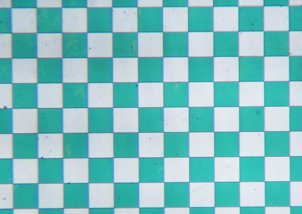
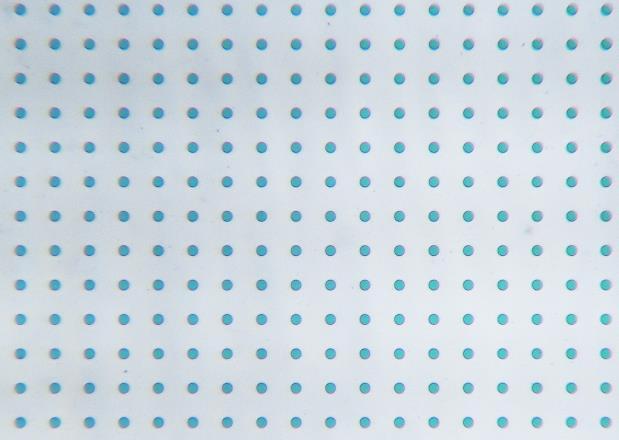
13 MetroChip manufacturing process Fabricated using advanced semiconductor processing methods 1. A protective layer is applied to heterostructure 2. Protective layer is eposed to light through a mask and developed 3. Poly-crystalline Si surface under mask is etched 4. Protective layer is removed revealing features derived from NIST certified mask Protective layer Polysilicon (150 nm) SiO 2 (5 nm) Si wafer This method can very reliably reproduce periodic structures sample-to-sample SEM Magnification Calibration 13
14 The Nuances of Periodic Structures Pitch = linewidth + spacewidth MetroBoost guarantees pitch, but DOES NOT guarantee linewidth Pitch reproducibility sample-to-sample is 2 parts per million Features such as line and space widths can vary as much as +/- 10 %. SEM Magnification Calibration 14
 Used line")

15 Metro Chip Certification by NIST NIST demonstrated that the pitch reliability of MetroBoost s mask is very high Deviation is only 2 ppm NIST then certified the pitch accuracy for a single metro chip (July 12, 2005) Used line scale interferometer This means that the pitch for ALL metro chips is BOTH accurate and reliable! Height, linewidth, and sidewall angle were not certified These features can vary up to +/- 10 % 120 μm SEM Magnification Calibration 15


16 Calibration Procedure via MetroChip Most vendors perform annual preventive maintenance activities Older SEMs have scan generators that can be adjusted via potentiometers by the service engineer Newer SEMs are corrected digitally during the mapping process within the SEM operation software Some vendors will perform calibrations with traceable SRM to a recognized authority (NMI), but others will not It is a good idea to perform your verification while the service engineer is still on site, since you will need their help if the verification fails SEM Magnification Calibration 16

17 Magnification Calibration Verification with Metro Chip 1. Set up your instrument for SEM imaging with Metro Chip installed 2. Locate the calibration rulings on the Metro Chip for both and y orientations 3. Capture images of both the and y oriented rulings without rotating your scan or stage 4. Calculate the percent error with the formula % error = 100 known value measured value known value 5. Make sure the distances measured in both and y directions meet your acceptance criteria (5 %) 6. This will verify that both and y are accurate and not distorted Pitch # Meas Known % Error Pitch = 250 nm SEM Magnification Calibration 17


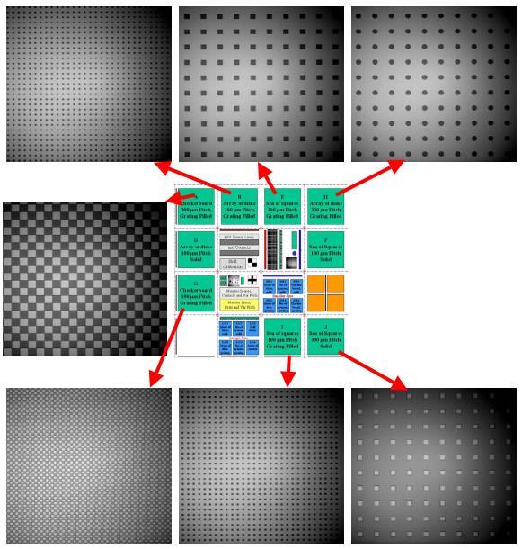

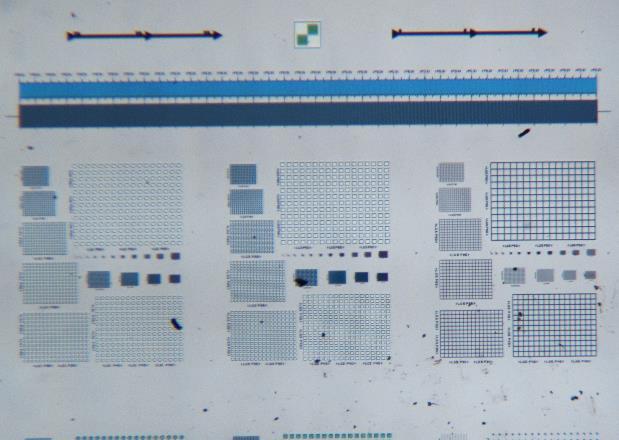
18 MetroChip Features and Uses 1. Linear Microscales 2. Scatterometry and Measurement Features 3. Distortion Targets SEM Magnification Calibration 18
. Any HF dip will attack the oide and should be avoided.")
19 Cleaning and Maintenance Things to avoid: Wiping the sample with a cloth. This will destroy the features. Spaying the sample with gases that leave residues. Also immersing the sample in liquids that leave residues. Using cleaning solutions that attack silicon dioide (glass). Any HF dip will attack the oide and should be avoided. Avoid plasma treatments that attack silicon dioide (glass). The list includes gas mitures containing CF 4 or CHF 3 or similar gases. Harsher plasma treatments, such as those using chlorinated gases, should be avoided since the polysilicon can be etched. Good cleaning procedures: Large particles can be blown off the sample by nitrogen gas sprayed from a nozzle, i.e. Dust-off. Rinsing the sample in DI water is safe and effective for removing larger particles. For cleaning fingerprints, chemical baths that remove photoresist, if available, are effective. Any resist strip used in semiconductor manufacturing is safe, including sulfuric peroide. One can also use plasma sample cleaners with pure oygen, or mitures of oygen and forming gas (N 2 /H 2 ) for removing fingerprints and also for cleaning hydrocarbon residues formed as a result of inspection in a scanning electron microscope. SEM Magnification Calibration 19


20 MAG*I*CAL for TEM magnification calibration Cross-sectional TEM sample with alternating layers of Si-Ge and Si. Grown via molecular beam epitay (MBE) Four sets of 5 alternating layers make for a wide range of image magnifications. Si-Ge layers are about 10 nm thin Since the heterostructure is epitaial, phase contrast imaging can also be used for HRTEM calibration and diffraction mode camera length calibration. SEM Magnification Calibration 20

21 Thank you for joining us. Mark A. Koten, Ph.D. Senior Research Scientist (630) SEM Magnification Calibration
22 The NIST Line Scale Interferometer A detailed eplanation is available on the NIST website at: SEM Magnification Calibration 22
Nanometers and Picometers: Keys to Success with 5 Terabit/in 2 Patterned Media
 Nanometers and Picometers: Keys to Success with 5 Terabit/in 2 Patterned Media Donald A. Chernoff Advanced Surface Microscopy Inc. Indianapolis, IN USA www.asmicro.com 2/10/2009 IDEMA Technical Symposium
NEBB Instrument Master List (Effective January 1, 2019)
") Discipline Function RC Air Pressure 0 in wg 0 Pa to to 10 in wg 2% of reading ± 0.001 2500 Pa 2% of reading ± 0.25 in wg Pa 0.001 in wg < 1 in wg 0.01 in wg > 1 in wg 0.10 Pa < 250 Pa 10 Pa > 250 Pa Air
Discipline Function RC Air Pressure 0 in wg 0 Pa to to 10 in wg 2% of reading ± 0.001 2500 Pa 2% of reading ± 0.25 in wg Pa 0.001 in wg < 1 in wg 0.01 in wg > 1 in wg 0.10 Pa < 250 Pa 10 Pa > 250 Pa Air
Keysight Technologies Optical Power Meter Head Special Calibrations. Brochure
 Keysight Technologies Optical Power Meter Head Special Calibrations Brochure Introduction The test and measurement equipment you select and maintain in your production and qualification setups is one of
M. Senoner 1), Th. Wirth 1), W. E. S. Unger 1), M. Escher 2), N. Weber 2), D. Funnemann 3) and B. Krömker 3) INTRODUCTION
, Th. Wirth 1), W. E. S. Unger 1), M. Escher 2), N. Weber 2), D. Funnemann 3) and B. Krömker 3) INTRODUCTION") Testing of Lateral Resolution in the Nanometre Range Using the BAM-L002 - Certified Reference Material: Application to ToF-SIMS IV and NanoESCA Instruments M. Senoner 1), Th. Wirth 1), W. E. S. Unger 1),
Testing of Lateral Resolution in the Nanometre Range Using the BAM-L002 - Certified Reference Material: Application to ToF-SIMS IV and NanoESCA Instruments M. Senoner 1), Th. Wirth 1), W. E. S. Unger 1),
Introduction of New Products
 Field Emission Electron Microscope JEM-3100F For evaluation of materials in the fields of nanoscience and nanomaterials science, TEM is required to provide resolution and analytical capabilities that can
Basic Functional Analysis. Sample Report Richmond Road, Suite 500, Ottawa, ON K2H 5B7 Canada Tel:
 Basic Functional Analysis Sample Report 3685 Richmond Road, Suite 500, Ottawa, ON K2H 5B7 Canada Tel: 613-829-0414 www.chipworks.com Basic Functional Analysis Sample Report Some of the information in this
Part 5-1: Lithography
 Part 5-1: Lithography Yao-Joe Yang 1 Pattern Transfer (Patterning) Types of lithography systems: Optical X-ray electron beam writer (non-traditional, no masks) Two-dimensional pattern transfer: limited
Bringing Answers to the Surface
 3D Bringing Answers to the Surface 1 Expanding the Boundaries of Laser Microscopy Measurements and images you can count on. Every time. LEXT OLS4100 Widely used in quality control, research, and development
Goodix GF6648 Touch Fingerprint Sensor. Exploratory Analysis
 Goodix GF6648 Exploratory Analysis 2 Some of the information in this report may be covered by patents, mask and/or copyright protection. This report should not be taken as an inducement to infringe on
AKM AK8973 and AK Axis Electronic Compass
 AKM AK8973 and AK8974 Process Review For comments, questions, or more information about this report, or for any additional technical needs concerning semiconductor and electronics technology, please call
Module 2: CMOS FEOL Analysis
 Module 2: CMOS FEOL Analysis Manufacturer Device # 2 About Chipworks Chipworks is the recognized leader in reverse engineering and patent infringement analysis of semiconductors and electronic systems.
STMicroelectronics VL53L0B ToF Proximity Sensor
 STMicroelectronics VL53L0B Basic Functional Analysis 1891 Robertson Road, Suite 500, Ottawa, ON K2H 5B7 Canada Tel: 613-829-0414 chipworks.com Basic Functional Analysis 2 Some of the information in this
Major Fabrication Steps in MOS Process Flow
 Major Fabrication Steps in MOS Process Flow UV light Mask oxygen Silicon dioxide photoresist exposed photoresist oxide Silicon substrate Oxidation (Field oxide) Photoresist Coating Mask-Wafer Alignment
Key Photolithographic Outputs
 Exposure latitude Depth of Focus Exposure latitude Vs DOF plot Linearity and MEEF Isolated-Dense Bias NILS Contrast Swing Curve Reflectivity Curve 1 Exposure latitude:the range of exposure energies (usually
The End of Thresholds: Subwavelength Optical Linewidth Measurement Using the Flux-Area Technique
 The End of Thresholds: Subwavelength Optical Linewidth Measurement Using the Flux-Area Technique Peter Fiekowsky Automated Visual Inspection, Los Altos, California ABSTRACT The patented Flux-Area technique
Bosch Sensortec BMI160 Low Power IMU
 Bosch Sensortec BMI160 Basic Functional Analysis 1891 Robertson Road, Suite 500, Ottawa, ON K2H 5B7 Canada Tel: 613-829-0414 chipworks.com Basic Functional Analysis 2 Some of the information in this report
D U A L S T E P H E I G H T. Calibration Standards
 D U A L S T E P H E I G H T Calibration Standards S I M P L Y T H E B E S T PSI Standards Move into the future of step height calibration and ISO compliance with PSI Standards Process Specialties introduces
Length section: New calibration and research services
 Length section: New calibration and research services O Kruger October 2015 T026 Overview Traditional traceability chart Traceability chart with length R&D projects Overview of Various R&D projects Conclusion
Publishable JRP Summary for Project T4 J03 JOSY. Next generation of quantum voltage systems for wide range applications
 Publishable JRP Summary for Project T4 J3 JOSY Next generation of quantum voltage systems for wide range applications The main objective of this project is to introduce quantum-based measurement systems
Layout Analysis Floorplan
 Sample Report Analysis from a Touch Screen Controller For any additional technical needs concerning semiconductor and electronics technology, please call Sales at Chipworks. 3685 Richmond Road, Suite 500,
membrane sample EUV characterization
 membrane sample EUV characterization Christian Laubis, PTB Outline PTB's synchrotron radiation lab Scatter from structures Scatter from random rough surfaces Measurement geometries SAXS Lifetime testing
CMOS Digital Integrated Circuits Lec 2 Fabrication of MOSFETs
 CMOS Digital Integrated Circuits Lec 2 Fabrication of MOSFETs 1 CMOS Digital Integrated Circuits 3 rd Edition Categories of Materials Materials can be categorized into three main groups regarding their
Manufacturer Part Number. Module 4: CMOS SRAM Analysis
 Manufacturer Part Number description Module 4: CMOS SRAM Analysis Manufacturer Device # 2 Some of the information is this report may be covered by patents, mask and/or copyright protection. This report
Scanning electron microscope
 Scanning electron microscope 5 th CEMM workshop Maja Koblar, Sc. Eng. Physics Outline The basic principle? What is an electron? Parts of the SEM Electron gun Electromagnetic lenses Apertures Detectors
Scanning electron microscope
 Scanning electron microscope 6 th CEMM workshop Maja Koblar, Sc. Eng. Physics Outline The basic principle? What is an electron? Parts of the SEM Electron gun Electromagnetic lenses Apertures Chamber and
Computer Generated Holograms for Optical Testing
 Computer Generated Holograms for Optical Testing Dr. Jim Burge Associate Professor Optical Sciences and Astronomy University of Arizona jburge@optics.arizona.edu 520-621-8182 Computer Generated Holograms
Photolithography Technology and Application
 Photolithography Technology and Application Jeff Tsai Director, Graduate Institute of Electro-Optical Engineering Tatung University Art or Science? Lind width = 100 to 5 micron meter!! Resolution = ~ 3
FABRICATION OF CMOS INTEGRATED CIRCUITS. Dr. Mohammed M. Farag
 FABRICATION OF CMOS INTEGRATED CIRCUITS Dr. Mohammed M. Farag Outline Overview of CMOS Fabrication Processes The CMOS Fabrication Process Flow Design Rules Reference: Uyemura, John P. "Introduction to
Peter Dack, Vice President Sales & Marketing Radian Research, Inc.
 Peter Dack, Vice President Sales & Marketing pdack@radianresearch.com Radian Research, Inc. Radian Research, Inc. is a world leader in State of the Art energy measurement instrumentation. Radian designs,
Nanofluidic Diodes based on Nanotube Heterojunctions
 Supporting Information Nanofluidic Diodes based on Nanotube Heterojunctions Ruoxue Yan, Wenjie Liang, Rong Fan, Peidong Yang 1 Department of Chemistry, University of California, Berkeley, CA 94720, USA
SCANNING ELECTRON MICROSCOPE (SEM) INSPECTION OF SEMICONDUCTOR DICE. ESCC Basic Specification No
 INSPECTION OF SEMICONDUCTOR DICE. ESCC Basic Specification No") Page 1 of 24 SCANNING ELECTRON MICROSCOPE (SEM) INSPECTION OF SEMICONDUCTOR DICE ESCC Basic Specification Issue 2 February 2014 Document Custodian: European Space Agency see https://escies.org PAGE 2 LEGAL
Page 1 of 24 SCANNING ELECTRON MICROSCOPE (SEM) INSPECTION OF SEMICONDUCTOR DICE ESCC Basic Specification Issue 2 February 2014 Document Custodian: European Space Agency see https://escies.org PAGE 2 LEGAL
Manufacturing Metrology Team
 The Team has a range of state-of-the-art equipment for the measurement of surface texture and form. We are happy to discuss potential measurement issues and collaborative research Manufacturing Metrology
Monolithically integrated InGaAs nanowires on 3D. structured silicon-on-insulator as a new platform for. full optical links
 Monolithically integrated InGaAs nanowires on 3D structured silicon-on-insulator as a new platform for full optical links Hyunseok Kim 1, Alan C. Farrell 1, Pradeep Senanayake 1, Wook-Jae Lee 1,* & Diana.
NANO 703-Notes. Chapter 9-The Instrument
 1 Chapter 9-The Instrument Illumination (condenser) system Before (above) the sample, the purpose of electron lenses is to form the beam/probe that will illuminate the sample. Our electron source is macroscopic
Microwave measurements for planar circuits and components: State of the art and future directions. Dr. Uwe Arz PTB
 Microwave measurements for planar circuits and components: State of the art and future directions Dr. Uwe Arz PTB Outline Previous work at PTB The EMPIR Initiative EMPIR Project 14IND02 PlanarCal 2 Why
Lithography Simulation Tools Needed for 22nm HP and Beyond. Chris Mack
 Lithography Simulation Tools Needed for 22nm HP and Beyond Chris Mack www.lithoguru.com Slicing the Pie Simulation Tool Characteristics Precision Accuracy Capabilities (speed, features) Simulation Tool
CHAPTER TWO METALLOGRAPHY & MICROSCOPY
 CHAPTER TWO METALLOGRAPHY & MICROSCOPY 1. INTRODUCTION: Materials characterisation has two main aspects: Accurately measuring the physical, mechanical and chemical properties of materials Accurately measuring
Section 2: Lithography. Jaeger Chapter 2 Litho Reader. The lithographic process
 Section 2: Lithography Jaeger Chapter 2 Litho Reader The lithographic process Photolithographic Process (a) (b) (c) (d) (e) (f) (g) Substrate covered with silicon dioxide barrier layer Positive photoresist
Leading in Desktop SEM Imaging and Analysis
 Leading in Desktop SEM Imaging and Analysis Fast. Outstanding. Reliable SEM imaging and analysis. The Phenom: World s Fastest Scanning Electron Microscope With its market-leading Phenom desktop Scanning
Lecture 0: Introduction
 Lecture 0: Introduction Introduction Integrated circuits: many transistors on one chip. Very Large Scale Integration (VLSI): bucketloads! Complementary Metal Oxide Semiconductor Fast, cheap, low power
Certificate of Calibration
 Certificate of Calibration ISO/IEC 17025:2005 Certificate Number 1-5607144213-1 Model Number Manufacturer Description Serial Number 34401A Keysight Technologies Inc Digital multimeter, 6.5 digit MY41007563
Section 2: Lithography. Jaeger Chapter 2 Litho Reader. EE143 Ali Javey Slide 5-1
 Section 2: Lithography Jaeger Chapter 2 Litho Reader EE143 Ali Javey Slide 5-1 The lithographic process EE143 Ali Javey Slide 5-2 Photolithographic Process (a) (b) (c) (d) (e) (f) (g) Substrate covered
MICROBUMP CREATION SYSTEM FOR ADVANCED PACKAGING APPLICATIONS
 MICROBUMP CREATION SYSTEM FOR ADVANCED PACKAGING APPLICATIONS Andrew Ahr, EKC Technology, & Chester E. Balut, DuPont Electronic Technologies Alan Huffman, RTI International Abstract Today, the electronics
Copyright 2000 Society of Photo Instrumentation Engineers.
 Copyright 2000 Society of Photo Instrumentation Engineers. This paper was published in SPIE Proceedings, Volume 4043 and is made available as an electronic reprint with permission of SPIE. One print or
LYNXEYE XE. Innovation with Integrity. High-Resolution Energy-Dispersive Detector for 0D, 1D, and 2D Diffraction XRD
 High-Resolution Energy-Dispersive Detector for 0D, 1D, and 2D Diffraction The is the first energy dispersive 0D, 1D, and 2D detector operating at room temperature for ultra fast X-ray diffraction measurements.
ELECTRON MICROSCOPY AN OVERVIEW
 ELECTRON MICROSCOPY AN OVERVIEW Anjali Priya 1, Abhishek Singh 2, Nikhil Anand Srivastava 3 1,2,3 Department of Electrical & Instrumentation, Sant Longowal Institute of Engg. & Technology, Sangrur, India.
Development of JEM-2800 High Throughput Electron Microscope
 Development of JEM-2800 High Throughput Electron Microscope Mitsuhide Matsushita, Shuji Kawai, Takeshi Iwama, Katsuhiro Tanaka, Toshiko Kuba and Noriaki Endo EM Business Unit, JEOL Ltd. Electron Optics
Advancing EDS Analysis in the SEM Quantitative XRF. International Microscopy Congress, September 5 th, Outline
 Advancing EDS Analysis in the SEM with in-situ Quantitative XRF Brian J. Cross (1) & Kenny C. Witherspoon (2) 1) CrossRoads Scientific, El Granada, CA 94018, USA 2) ixrf Systems, Inc., Houston, TX 77059,
Certificate of Calibration
 Certificate of Calibration ISO/IEC 17025:2005 and ANSI/NCSL Z540.1-1994 Model Number Manufacturer Description Serial Number Customer Asset No. 11667A Keysight Technologies Inc DC-18 GHz power splitter,
Module 4B7: VLSI Design, Technology, and CAD. Scanning Electron Microscopical Examination of CMOS Integrated Circuit
 Engineering Tripos Part IIB FOURTH YEAR Module 4B7: VLSI Design, Technology, and CAD Laboratory Experiment Dr D Holburn and Mr B Breton Scanning Electron Microscopical Examination of CMOS Integrated Circuit
Measurement of Microscopic Three-dimensional Profiles with High Accuracy and Simple Operation
 238 Hitachi Review Vol. 65 (2016), No. 7 Featured Articles Measurement of Microscopic Three-dimensional Profiles with High Accuracy and Simple Operation AFM5500M Scanning Probe Microscope Satoshi Hasumura
Observing Microorganisms through a Microscope LIGHT MICROSCOPY: This type of microscope uses visible light to observe specimens. Compound Light Micros
 PHARMACEUTICAL MICROBIOLOGY JIGAR SHAH INSTITUTE OF PHARMACY NIRMA UNIVERSITY Observing Microorganisms through a Microscope LIGHT MICROSCOPY: This type of microscope uses visible light to observe specimens.
Development of a LFLE Double Pattern Process for TE Mode Photonic Devices. Mycahya Eggleston Advisor: Dr. Stephen Preble
 Development of a LFLE Double Pattern Process for TE Mode Photonic Devices Mycahya Eggleston Advisor: Dr. Stephen Preble 2 Introduction and Motivation Silicon Photonics Geometry, TE vs TM, Double Pattern
Certified Reference Materials for UV, Visible, NIR and IR Molecular Spectroscopy
 Certified Reference Materials for UV, Visible, NIR and IR Molecular Spectroscopy RM-1N3N5DHG Set Serial No: 23135 Customer Details: Starna Cells Inc 5950 Traffic Way Atascadero CA 93422 U.S.A. The customer
Deliverable D5.2 DEMO chip processing option 3
 Deliverable D5.2 DEMO chip processing option 3 Deliverable D5.2 DEMO chip processing Option 3 Date: 22-03-2017 PiezoMAT 2017-03-22_Delivrable_D5.2 Author(s): E.Saoutieff; M.Allain (CEA) Participant(s):
DOE Project: Resist Characterization
 DOE Project: Resist Characterization GOAL To achieve high resolution and adequate throughput, a photoresist must possess relatively high contrast and sensitivity to exposing radiation. The objective of
SMD ENS Metrology - National Standards. Short overview. Hugo Pirée. World Metrology Day 2018 Brussels.
 SMD ENS Metrology - National Standards Short overview Hugo Pirée World Metrology Day 2018 Brussels Federal government FPS ECONOMY Gen. Direction QUALITY & SAFETY Division METROLOGY 14 persons National
to Measure is to Know but how to measure?
 to Measure is to Know but how to measure? Gert Rietveld Nederlands Meetinstituut Delft GRietveld@NMi.nl VKRT meeting 8 Feb 2007-1 Nederlands Meetinstituut Legal inspection Testing and certification Scientific
Examination, TEN1, in courses SK2500/SK2501, Physics of Biomedical Microscopy,
 KTH Applied Physics Examination, TEN1, in courses SK2500/SK2501, Physics of Biomedical Microscopy, 2009-06-05, 8-13, FB51 Allowed aids: Compendium Imaging Physics (handed out) Compendium Light Microscopy
EE143 Fall 2016 Microfabrication Technologies. Lecture 3: Lithography Reading: Jaeger, Chap. 2
 EE143 Fall 2016 Microfabrication Technologies Lecture 3: Lithography Reading: Jaeger, Chap. 2 Prof. Ming C. Wu wu@eecs.berkeley.edu 511 Sutardja Dai Hall (SDH) 1-1 The lithographic process 1-2 1 Photolithographic
CHAPTER 2 POLARIZATION SPLITTER- ROTATOR BASED ON A DOUBLE- ETCHED DIRECTIONAL COUPLER
 CHAPTER 2 POLARIZATION SPLITTER- ROTATOR BASED ON A DOUBLE- ETCHED DIRECTIONAL COUPLER As we discussed in chapter 1, silicon photonics has received much attention in the last decade. The main reason is
End-of-line Standard Substrates For the Characterization of organic
 FRAUNHOFER INSTITUTe FoR Photonic Microsystems IPMS End-of-line Standard Substrates For the Characterization of organic semiconductor Materials Over the last few years, organic electronics have become
Uncertainty in measurements of micro-patterned thin film thickness using Nanometrological AFM - Reliability of parameters for base straight line -
 Uncertainty in measurements of micro-patterned thin film thickness using Nanometrological AFM - Reliability of parameters for base straight line - Ichiko Misumi,, Satoshi Gonda, Tomizo Kurosawa, Yasushi
Section 2: Lithography. Jaeger Chapter 2. EE143 Ali Javey Slide 5-1
 Section 2: Lithography Jaeger Chapter 2 EE143 Ali Javey Slide 5-1 The lithographic process EE143 Ali Javey Slide 5-2 Photolithographic Process (a) (b) (c) (d) (e) (f) (g) Substrate covered with silicon
Fabricating 2.5D, 3D, 5.5D Devices
 Fabricating 2.5D, 3D, 5.5D Devices Bob Patti, CTO rpatti@tezzaron.com Tezzar on Semiconduct or 04/15/2013 1 Gen4 Dis-Integrated 3D Memory DRAM layers 42nm node 2 million vertical connections per lay per
450mm and Moore s Law Advanced Packaging Challenges and the Impact of 3D
 450mm and Moore s Law Advanced Packaging Challenges and the Impact of 3D Doug Anberg VP, Technical Marketing Ultratech SOKUDO Lithography Breakfast Forum July 10, 2013 Agenda Next Generation Technology
Introduction to Electron Microscopy
 Introduction to Electron Microscopy Prof. David Muller, dm24@cornell.edu Rm 274 Clark Hall, 255-4065 Ernst Ruska and Max Knoll built the first electron microscope in 1931 (Nobel Prize to Ruska in 1986)
UV Nanoimprint Stepper Technology: Status and Roadmap. S.V. Sreenivasan Sematech Litho Forum May 14 th, 2008
 UV Nanoimprint Stepper Technology: Status and Roadmap S.V. Sreenivasan Sematech Litho Forum May 14 th, 2008 Overview Introduction Stepper technology status: Patterning and CD Control Through Etch Alignment
(Refer Slide Time: 00:10)
") Fundamentals of optical and scanning electron microscopy Dr. S. Sankaran Department of Metallurgical and Materials Engineering Indian Institute of Technology, Madras Module 03 Unit-6 Instrumental details
Fundamentals of optical and scanning electron microscopy Dr. S. Sankaran Department of Metallurgical and Materials Engineering Indian Institute of Technology, Madras Module 03 Unit-6 Instrumental details
VLSI Design. Introduction
 VLSI Design Introduction Outline Introduction Silicon, pn-junctions and transistors A Brief History Operation of MOS Transistors CMOS circuits Fabrication steps for CMOS circuits Introduction Integrated
New CD-SEM System for 100-nm Node Process
 New CD-SEM System for 100-nm Node Process Hitachi Review Vol. 51 (2002), No. 4 125 Osamu Nasu Katsuhiro Sasada Mitsuji Ikeda Makoto Ezumi OVERVIEW: With the semiconductor device manufacturing industry
Errata to Procedural Standard for Sound & Vibration Measurement 2015 Third Edition
 Errata to Procedural Standard for Sound & Vibration Measurement 2015 Third Edition Correction Sheet #1 Issued 01 July 2018 Copyright 2018 by NEBB All rights reserved. Published 2018. Printed in the United
19th Meeting of the Directors of NMIs and Member State Representatives with BIPM
 19th Meeting of the Directors of NMIs and Member State Representatives with BIPM Session on Advanced Manufacturing, Digitization and Internet of Things Thursday, 19 th October 2017 11:10 to 13:00 Advanced
Low Voltage Electron Microscope
 LVEM5 Low Voltage Electron Microscope Nanoscale from your benchtop LVEM5 Delong America DELONG INSTRUMENTS COMPACT BUT POWERFUL The LVEM5 is designed to excel across a broad range of applications in material
Transmission Electron Microscopy 9. The Instrument. Outline
 Transmission Electron Microscopy 9. The Instrument EMA 6518 Spring 2009 02/25/09 Outline The Illumination System The Objective Lens and Stage Forming Diffraction Patterns and Images Alignment and Stigmation
Physikalisch Technische Bundesanstalt
 EURAMET Intercomparison: Involute Gear Artifacts 1 Physikalisch Technische Bundesanstalt EURAMET Intercomparison Involute Gear Artifacts Technical Protocol Rev 3 EURAMET Intercomparison: Involute Gear
Chapter 7. Optical Measurement and Interferometry
 Chapter 7 Optical Measurement and Interferometry 1 Introduction Optical measurement provides a simple, easy, accurate and reliable means for carrying out inspection and measurements in the industry the
optical and photoresist effects
 Focus effects in submicron optical lithography, optical and photoresist effects Chris A. Mack and Patricia M. Kaufman Department of Defense Fort Meade, Maryland 20755 Abstract This paper gives a review
Deliverable 4.2: TEM cross sections on prototyped Gated Resistors
 Deliverable 4.2: TEM cross sections on prototyped Gated Resistors Olga G. Varona, Geoff Walsh, Bernie Capraro Intel Ireland 21 June 2011 Abbreviation list D: drain FIB: focused ion-beam HRTEM: high resolution
Keysight Technologies Why Magnification is Irrelevant in Modern Scanning Electron Microscopes. Application Note
 Keysight Technologies Why Magnification is Irrelevant in Modern Scanning Electron Microscopes Application Note Introduction From its earliest inception, the Scanning Electron Microscope (SEM) has been
Absolute distance interferometer in LaserTracer geometry
 Absolute distance interferometer in LaserTracer geometry Corresponding author: Karl Meiners-Hagen Abstract 1. Introduction 1 In this paper, a combination of variable synthetic and two-wavelength interferometry
Micro- and Nano- Fabrication and Replication Techniques
 Micro- and Nano- Fabrication and Replication Techniques Why do we have to write thing small and replicate fast? Plenty of Room at the Bottom Richard P. Feynman, December 1959 How do we write it? We have
Specifying and Measuring Nanometer Surface Properties. Alson E. Hatheway
 Specifying and Measuring Nanometer Surface Properties a seminar prepared for the American Society of Mechanical Engineers 93663a.p65(1 Alson E. Hatheway Alson E. Hatheway Inc. 787 West Woodbury Road Unit
Lecture 7. Lithography and Pattern Transfer. Reading: Chapter 7
 Lecture 7 Lithography and Pattern Transfer Reading: Chapter 7 Used for Pattern transfer into oxides, metals, semiconductors. 3 types of Photoresists (PR): Lithography and Photoresists 1.) Positive: PR
STRUCTURE OF THE MICROSCOPE
 STRUCTURE OF THE MICROSCOPE Use the word list to label the microscope below: Light Source Coarse adjustment knob Diaphragm Stage Clips Objectives Fine Adjustment Knob Base Stage Stage Clips Arm Revolving
SITRANS F flowmeters. SITRANS F M System information MAGFLO electromagnetic flowmeters. 4/18 Siemens FI
 Function All are based on Faraday s law of induction: U M = B v d k U M = Measured voltage induced in the medium perpendicular to the magnetic field and the flow direction. The voltage is tapped at two
Outline: Introduction: What is SPM, history STM AFM Image treatment Advanced SPM techniques Applications in semiconductor research and industry
 1 Outline: Introduction: What is SPM, history STM AFM Image treatment Advanced SPM techniques Applications in semiconductor research and industry 2 Back to our solutions: The main problem: How to get nm
Results of Proof-of-Concept 50keV electron multi-beam Mask Exposure Tool (emet POC)
") Results of Proof-of-Concept 50keV electron multi-beam Mask Exposure Tool (emet POC) Elmar Platzgummer *, Christof Klein, and Hans Loeschner IMS Nanofabrication AG Schreygasse 3, A-1020 Vienna, Austria
Results of Proof-of-Concept 50keV electron multi-beam Mask Exposure Tool (emet POC) Elmar Platzgummer *, Christof Klein, and Hans Loeschner IMS Nanofabrication AG Schreygasse 3, A-1020 Vienna, Austria
Institute of Solid State Physics. Technische Universität Graz. Lithography. Peter Hadley
 Technische Universität Graz Institute of Solid State Physics Lithography Peter Hadley http://www.cleanroom.byu.edu/virtual_cleanroom.parts/lithography.html http://www.cleanroom.byu.edu/su8.phtml Spin coater
Low-energy Electron Diffractive Imaging for Three dimensional Light-element Materials
 Low-energy Electron Diffractive Imaging for Three dimensional Light-element Materials Hitachi Review Vol. 61 (2012), No. 6 269 Osamu Kamimura, Ph. D. Takashi Dobashi OVERVIEW: Hitachi has been developing
Chapter 3 Fabrication
 Chapter 3 Fabrication The total structure of MO pick-up contains four parts: 1. A sub-micro aperture underneath the SIL The sub-micro aperture is used to limit the final spot size from 300nm to 600nm for
Project Staff: Timothy A. Savas, Michael E. Walsh, Thomas B. O'Reilly, Dr. Mark L. Schattenburg, and Professor Henry I. Smith
 9. Interference Lithography Sponsors: National Science Foundation, DMR-0210321; Dupont Agreement 12/10/99 Project Staff: Timothy A. Savas, Michael E. Walsh, Thomas B. O'Reilly, Dr. Mark L. Schattenburg,
PicoMaster 100. Unprecedented finesse in creating 3D micro structures. UV direct laser writer for maskless lithography
 UV direct laser writer for maskless lithography Unprecedented finesse in creating 3D micro structures Highest resolution in the market utilizing a 405 nm diode laser Structures as small as 300 nm 375 nm
SCOPE OF ACCREDITATION TO ISO/IEC 17025:2005 & ANSI/NCSL Z
 SCOPE OF ACCREDITATION TO ISO/IEC 17025:2005 & ANSI/NCSL Z540-1-1994 DIGITAL MEASUREMENT METROLOGY INC. (A TRESCAL COMPANY) 26 Automatic Road, Unit 4 Brampton, Ontario, CANADA L6S 5N7 Nana Mantey Phone:
Foreign Particulate Matter testing using the Morphologi G3
 Foreign Particulate Matter testing using the Morphologi G3 Introduction The Morphologi G3 with its Foreign Particle Detection capabilities allows the detection, enumeration and size classification of foreign
EE 330 Lecture 7. Design Rules. IC Fabrication Technology Part 1
 EE 330 Lecture 7 Design Rules IC Fabrication Technology Part 1 Review from Last Time Technology Files Provide Information About Process Process Flow (Fabrication Technology) Model Parameters Design Rules
Sensor Fusion Enables Comprehensive Analysis of Laser Processing in Additive Manufacturing
 MKS Instruments 1 of 6 Sensor Fusion Enables Comprehensive Analysis of Laser Processing in Additive Manufacturing By Kevin Kirkham, Senior Manager, Product Development, Ophir Sensor: "A device that detects
Indiana University JEM-3200FS
 Indiana University JEM-3200FS Installation Specification Model: JEM 3200FS Serial Number: EM 15000013 Objective Lens Configuration: High Resolution Pole Piece (HRP) JEOL Engineer: Michael P. Van Etten
5. Lithography. 1. photolithography intro: overall, clean room 2. principle 3. tools 4. pattern transfer 5. resolution 6. next-gen
 5. Lithography 1. photolithography intro: overall, clean room 2. principle 3. tools 4. pattern transfer 5. resolution 6. next-gen References: Semiconductor Devices: Physics and Technology. 2 nd Ed. SM
Transmission electron Microscopy
 Transmission electron Microscopy Image formation of a concave lens in geometrical optics Some basic features of the transmission electron microscope (TEM) can be understood from by analogy with the operation