NeoScope. Simple Operation to 40,000. Table Top SEM. Serving Advanced Technology
|
|
|
- Natalie Patterson
- 5 years ago
- Views:
Transcription


1 Table Top SEM Simple Operation to 40,000 Serving Advanced Technology


2 From 10 to 40,000 Table Top SEM Notebook PC version Just plug it to a wall outlet after placing it on a table Desktop PC version Option 2


3 Just a few suggestions Application as wide as your imagination Observation at higher magnification Larger depth of focus High magnification High resolution Magnification 0.5 1,500 Magnification 10 40,000 Check a specimen before sending it out to analytical lab Sampling inspection done with the ease of light microscope Products Good products Rejected products 1 Operation is easy. You can learn it in a short time. 2 High quality image by secondary electrons 3 Up to 70mm diameter 50mm height specimen 4 Measurement in nanometer 5 My recipe for reliable results 6 Smile View for quick report editing 7 Maintenance is easy 3
")


4 Sharp image at high magnification Larger depth of focus A scanning electron microscope (SEM) has about 10 times larger depth of focus so that you can focus even on an extremely rough specimen. You can understand complicated structures easily. Light microscope 500 Scanning electron microscope µm Mouse changes magnification continuously. No focus change when magnification is changed. Specimen : Fracture surface of brass screw Continuous zoom up from the lowest magnification High magnification image in no time 24 15, ,000 Specimen : Zinc oxide 4

 This is cement mix for DIY mixed with water and set for 30 minutes.")
 The specimen is conductive enough to be observed without conductive coating.")
 Gypsum was mixed with water and set for a few minutes.")
5 Realistic high magnification Table Top SEM 20,000 by secondary electron (SE) image in high vacuum JCM-5000 goes up to 20,000 and shows realistic surface image by secondary electron image at the high vacuum mode. The depth of focus is large enough to easily understand complicated morphology. The high vacuum mode keeps high performance for a long period of time. Cement, Secondary electron image, original mag: 20,000 (with coating) This is cement mix for DIY mixed with water and set for 30 minutes. Cement crystals are growing on sand grains. Gold conductive coating has been applied by a sputter coater. Zinc oxide, Secondary electron image, original mag: 20,000 (no coating) The specimen is conductive enough to be observed without conductive coating. You can observe particles smaller than 0.1micron (100nm). Gypsum, Secondary electron image, original mag: 20,000 (with coating) Gypsum was mixed with water and set for a few minutes. Fine long crystals are observed. Gold conductive coating has been applied by a sputter coater. Gypsum, Secondary electron image, original mag: 10,000 (with coating) A wider view was observed at a slightly lower magnification. Small particles are observed with long crystals. 5


6 Large specimen can be observed A small specimen is observed by putting it on a specimen mount. A large specimen up to 70mm diameter and 50mm height can be set on the 70mm specimen holder. You can use carbon double sticky tape to fix a specimen on a mounting block or a holder. Then set the specimen holder on the specimen stage. Closing the specimen stage starts pumping automatically. The specimen stage moves 35mm on both X and Y axes. The specimen stage is stable enough to show a clear image at 20,000. Maximum 70mm diameter 50mm height specimen. Pull out the specimen stage and set a specimen holder on it. Close the specimen stage starts pumping automatically. Specimen holder and specimen mount Specimen holder Standard specimen holder 25mm diameter specimen holder 70mm diameter specimen holder Optional specimen holder 35mm diameter specimen holder Tilting specimen holder 25mm diameter specimen holder* 70mm diameter specimen holder* 35mm diameter specimen holder Specimen mount 25mmDia 10mmH 25mmDia 25mmH 35mmDia 10mmH Pre-tilt specimen mount (custom made) 25mmDia 25mmH* 25mmDia 10mmH* Calibration specimen* *Standard 6


7 Table Top SEM Observation Let's observe in the high vacuum mode A secondary electron image appears automatically on the monitor when the specimen chamber is pumped to high vacuum. The operation condition is the Standard Recipe, which give good results for most of specimens at 10kV. This condition reveals fine surface structures of a specimen clearly. Observation monitor Observation made easy by the recipe The optimum operation conditions may vary depending on the material or shape of a specimen, or magnification for observation. Some specimens may produce better results by using an accelerating voltage or probe current different from the Standard Recipe. When you find a better operation conditions for your specimen, you can store them in My Recipe and reuse it when you observe a similar specimen later. 15kV : Suitable for high magnification 10kV : Suitable for fine structures up to a few thousand times 5kV : Suitable for heat sensitive specimen Specimens : Business card 7


8 Adjustment of image The contrast and brightness of image can be controlled automatically or manually. Automatic operation First click on the Auto Contrast & Brightness for automated adjustment. You can adjust contrast and brightness manually as well. Then click on the Auto Focus to focus the image. At high magnifications you may need to compensate astigmatism. Brightness Focus Manual operation Image adjustment You can adjust contrast and brightness manually as well. Focus Focus can be manually adjusted as well as automatically. Astigmatism correction Fine astigmatism adjustment is available in addition to the automatic correction. Image shift You can shift the image by a mouse drag. This is convenient at high magnification. IImage Rotation You can rotate a live image on the monitor by 1 degree step or 90 degree step. 8

 Images obtained by the SEM are pasted on a layout sheet of Smile View")


9 Measurement mode Table Top SEM You can measure a distance between two points just by a click on each point. The result is pasted on the image. 5.8 m 19º 5.1 m 33º 5.3 m 38º Click on two points on a image. The result is pasted on the image. Report Creation (Option) Images obtained by the SEM are pasted on a layout sheet of Smile View (Option) to create a report. The acquired images are displayed in small thumb nail images. Simply drag and drop these image onto a layout sheet. You can freely edit your own layout by changing the size of each image and position. Magnification is automatically calibrated and displayed as you change the size of image. SMile View also has a measurement mode. You can measure on a layout sheet and result is pasted on the report. Thumb nail images Layout sheet to edit a report 9
 is unique due to its large depth of focus")


 Tap,")
10 Large Depth of Focus Complicated morphology observed by SE image in high vacuum A scanning electron microscope (SEM) is unique due to its large depth of focus together with high resolution. You can observe clearly a rough specimen difficult for a light microscope to focus. The lowest magnification is 10. You can find an area located by a light microscope easily. BNC connector, Secondary electron image, original mag: 15 (no coating) BNC connector, Secondary electron image, original mag: 11 (no coating) Tap, Secondary electron image, original mag: 17 (no coating) Drill, Secondary electron image, original mag: 30 (no coating) 10


 Integrated circuit, Secondary")
")
11 Table Top SEM Industrial Products Quality control by high quality SE and BSE images An SEM lets you observe complicated structures clearly in details with high resolution. This unique feature of an SEM is widely used in the industry from research to quality control. Electronic board, Secondary electron image, original mag: 10 (with coating) Electronic board, Secondary electron image, original mag: 20 (with coating) Integrated circuit, Secondary electron image, original mag: 2,400 (no coating) Solder, Backscattered electron image, original mag: 3,000 (no coating) Contaminated contact surface, Secondary electron image, original mag: 100 (no coating) 11


, Secondary electron image,original mag: 500")

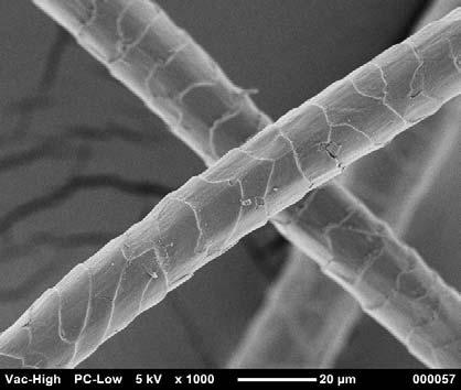
12 Industrial Products Quality control by high quality SE image in high vacuum An SEM is widely used in the industry from research to quality control. Medicine surface, Secondary electron image, original mag: 30 (with coating) Medicine cross section, Secondary electron image, original mag: 1,000 (with coating) Business card (left: printed, right: paper), Secondary electron image,original mag: 500 (with coating) Wool, Secondary electron image, original mag: 1,000 (with coating) Metal fracture, Secondary electron image, original mag: 5,000 (with coating) Optical film, Secondary electron image, original mag: 5,000 (with coating) 12


 270 (with coating) Dried tobacco leaf,")
")
13 Table Top SEM Plant Product High quality SE image with conductive coating Plant products such as lumber do not have electric conductivity. You can observe the surface structures in high precision with secondary electron image in the high vacuum mode by applying conductive coating. Dry wood cross section, Secondary electron image, original mag: 3,000 (with coating) Dry wood cross section, Secondary electron image, original mag: 270 (with coating) Dried tobacco leaf, Secondary electron image, original mag: 240 (with coating) Bamboo charcoal, Secondary electron image, original mag: 700 (with coating) Bamboo charcoal, Secondary electron image, original mag: 100 (with coating) 13


 150 (with coating) Fruit fly,")
 Fruit fly, Secondary electron image, original")
 14")
14 Insects Realistic image in SE image in high vacuum Fine structures of insects can be observed clearly in details at high magnification. The SE image is most suitable for observation of insects. Butterfly scale, Secondary electron image, original mag: 20,000 (with coating) Butterfly scale, Secondary electron image, original mag: 150 (with coating) Fruit fly, Secondary electron image, original mag: 24 (with coating) Fruit fly, Secondary electron image, original mag: 800 (with coating) Larva of butterfly, Secondary electron image, original mag: 200 (with coating) 14


 Red blood cell of")

15 Table Top SEM Animal Organism SE image in high vacuum Animal organism contains water and not suitable for observation in SEM. These specimens are prepared by chemical fixation, dehydration, and drying by freeze dry or by critical point dry. A dried specimen is applied with conductive coating and observed with SE image in high vacuum. Glomerulus, Secondary electron image, original mag: 5,000 (with coating) Lung alveolus of rat, Secondary electron image, original mag: 500 (with coating) Red blood cell of rat, Secondary electron image, original mag: 8,000 (with coating) Egg shell is observed. You can observe the fine inner network. You can observe fine holes on the crystal structures in the shell. Inner film of egg shell, Secondary electron image, original mag: 1,000 (with coating) Egg shell cross section, Secondary electron image, original mag: 2,000 (with coating) 15


, Secondary electron image,")
16 Non conductive specimens Observed with SE image in high vacuum You can observe a non-conductive specimen by using low voltage where the numbers of incident electrons and emitted electrons from a specimen are close or in the low vacuum mode by introducing small amount of air in the specimen chamber. In the low vacuum mode gas molecules are ionized by the incident electrons and neutralize the electrons accumulated on the specimen surface. Mold grown on paulowia leaf (no coating, frame accumulation), Secondary electron image, original mag: 100 Powdery mildew on horse chestnut (no coating, frame accumulation), Secondary electron image, original mag: 900 Alumina powder (no coating, frame accumulation), Secondary electron image, original mag: 2,000 Paper (no coating), Secondary electron image, original mag:


 image in the low vacuum mode.")
, BSE image in low vacuum, original mag: 1,000 Concrete cross section (no coating),")
17 Table Top SEM Non conductive specimens Observed in low vacuum When you introduce small amount of air into the specimen chamber to increase the pressure to 30Pa, about 10% of the incident electrons collide with gas molecules and generate ions. The ions neutralize the electrons accumulated on a non-conductive specimen surface. The electrons collieded with gas molecules are scattered and reach over a wide area on the specimen. You observe backscattered electron (BSE) image in the low vacuum mode. BSE images are of slightly poorer resolution due to larger generation volume of backscattered electrons. Face powder (no coating), BSE image in low vacuum, original mag: 1,000 Concrete cross section (no coating), BSE image in low vacuum, original mag: 200 Cloth (no coating), BSE image in low vacuum, original mag: 100 Paper (no coating), BSE image in low vacuum, original mag:


 You can obtain a")


18 Self Test and Simple Maintenance Neo cartridge Neo Scope can be easily maintained by a user. When the SEM is not functioning properly, you can find the reason on the Self test window. It is simple to change a filament. uses cartridge electron source, which is composed of electron gun and filament. Remove an old electron source and plug in a new one. You can change filament by simple procedure in a short time. Ring to hold electron gun Self test when a filament is burnt out, this window appears automatically. Electron gun with filament NeoCoater (Option) You can obtain a sharp and good quality image of a non-conductive specimen easily by applying conductive coating on a specimen. The conductive coating is only a few nm thick so that fine surface structures are not hidden. A sputter coater is used to apply conductive coating. You can form uniform coating film in a short time. NeoCoater Compact Easy to use Affordable Price Carbon specimen without conductive coating Carbon specimen with conductive coating of gold 18


 composition Main console Rotary pump PC NeoCoater composition")
19 Table Top SEM Principal Specifications Specifications Installation requirement Magnification Observation mode Electron source Accelerating voltage Specimen stage Specimen exchange Maximum specimen size Detector Computer OS Digital image Data display Automatic operation Evacuation time Evacuation system Main console dimensions 10 40,000 High vacuum mode, Low vacuum mode Small cartridge electron source 15kV, 10kV, 5kV Manual, X 35mm, Y 35mm Specimen stage draw out 70mm Diameter 50mm Height Secondary electron detector, Backscattered electron detector Portable PC Windows Vista, Windows 7 1,280 1,024 pixels, bmp, tif, jpg Accelerating voltage, magnification, micron bar, micron value Electron source, focus, brightness, contrast, and astigmatism Approximately 3 minutes TMP, RP W492 D458 H434mm Electric power Single phase AC100V (400VA) 240V (1,100VA) 50Hz/60Hz Power fluctuation Less than ±10% Grounding terminal One, 100 Ω or less Installation room Room temperature 15ºC 30ºC Humidity 70% or less Weight Main console Approximately 69kg PC Approximately 11kg RP Approximately 16kg Wagon to add mobility (Option) composition Main console Rotary pump PC NeoCoater composition Specifications NeoCoater NeoCoater Main console Composition Specimen table size Specimen table height Power Weight Operation vacuum Sputter time Target Main console + RP (20L/min) 70mm diameter 32mm to 73mm to the target Single phase 100V 50/60Hz 440W Main console 9.3kg + RP9kg 4Pa 1 min (standard), 2 min, 3 min selectable Au Rotary pump Target size Main console dimension ø mm W200 D230 H325mm *Specifications subject to change without notice. 19


20 Table Top SEM Specifications and equipment are subject to change without any notice or obligation on the part of the manufacturer NIKON CORPORATION The products detailed in the brochure are controlled by the Japanese Foreign Exchange and Foreign Trade Law and the International Export Control Regime. If there is a possibility that they may be utilized for the development of weapons of mass destruction, etc., they shall not be exported without authorization from the government. NIKON CORPORATION 6-3, Nishiohi 1-chome, Shinagawa-ku, Tokyo , Japan phone: fax: NIKON INSTRUMENTS INC Walt Whitman Road, Melville, N.Y , U.S.A. phone: ; NIKON (within the U.S.A. only) fax: NIKON INSTRUMENTS EUROPE B.V. Laan van Kronenburg 2, 1183 AS, Amstelveen, The Netherlands phone: fax: NIKON INSTRUMENTS (SHANGHAI) CO., LTD. CHINA phone: fax: (Beijing branch) phone: fax: (Guangzhou branch) phone: fax: Printed in Japan NIKON SINGAPORE PTE LTD. SINGAPORE phone: fax: NIKON MALAYSIA SDN. BHD. MALAYSIA phone: fax: NIKON INSTRUMENTS KOREA CO., LTD. KOREA phone: fax: NIKON CANADA INC. CANADA phone: fax: NIKON FRANCE S.A.S. FRANCE phone: fax: NIKON GMBH GERMANY phone: fax: NIKON INSTRUMENTS S.p.A. ITALY phone: fax: NIKON AG SWITZERLAND phone: fax: NIKON UK LTD. UNITED KINGDOM phone: fax: NIKON GMBH AUSTRIA AUSTRIA phone: fax: NIKON BELUX BELGIUM phone: fax:
INTRODUCTION We believe that every laboratory working in the field of nanotechnology needs an SEM, therefore we would like to introduce to you our IEM
 INTRODUCTION We believe that every laboratory working in the field of nanotechnology needs an SEM, therefore we would like to introduce to you our IEM series of SEM. In short space of time, our device
SCIENTIFIC INSTRUMENT NEWS. Introduction. Design of the FlexSEM 1000
 SCIENTIFIC INSTRUMENT NEWS 2017 Vol. 9 SEPTEMBER Technical magazine of Electron Microscope and Analytical Instruments. Technical Explanation The FlexSEM 1000: A Scanning Electron Microscope Specializing
Quick and simple installation and no maintenance needed. 3 Times More affordable Than a normal SEM. Obtaining results in less than 4 minutes
 INTRODUCTION We believe that every laboratory working in the field of nanotechnology needs an SEM, therefore we would like to introduce to you our IEM series of SEM. In short space of time, our device
Super High Vertical Resolution Non-Contact 3D Surface Profiler BW-S500/BW-D500 Series
 Super High Vertical Resolution Non-Contact 3D Surface Profiler BW-S500/BW-D500 Series Nikon's proprietary scanning-type optical interference measurement technology achieves 1pm* height resolution. * Height
Model SU3500 Scanning Electron Microscope
 Model SU3500 Scanning Electron Microscope Modified and Parts taken from Hitachi Easy Operation Guide. Before using the Model SU3500 SEM, be sure to read the [GENERAL SAFETY GUIDELINES] in the instruction
CNC Video Measuring System NEXIV VMZ-K series. CNC Video Measuring System. Confocal Model
 CNC Video Measuring System NEXIV VMZ-K series CNC Video Measuring System Confocal Model D FOV Measurements Generated with s A ground-breaking multifunctional video measuring system developed on the strength
Schottky Emission VP FE-SEM
 Schottky Emission VP FE-SEM Variable Pressure The Scanning Electron Microscope (SEM) has played an important role for many years for research and development of advanced materials in the leading edge of
Wafer Loaders for IC Inspection Microscopes NWL200 Series. Wafer Loaders for IC Inspection Microscopes
 Wafer Loaders for IC Inspection Microscopes NWL200 Wafer Loaders for IC Inspection Microscopes Wafer Loaders for IC Inspection Microscopes I Nikon s original technology ensures safe, reliable loading of
Confocal NEXIV VMZ-K Series. CNC Video Measuring System CONFOCAL NEXIV. VMZ-K Series
 Confocal NEXIV VMZ-K Series CNC Video Measuring System CONFOCAL NEXIV VMZ-K Series 3D FOV Measurements Generated with Confocal Images The Confocal NEXIV VMZ-K series, a ground-breaking multifunctional
Confocal NEXIV VMZ-K Series. CNC Video Measuring System CONFOCAL NEXIV. VMZ-K Series
 Confocal NEXIV VMZ-K Series CNC Video Measuring System CONFOCAL NEXIV VMZ-K Series The VMZ-K series enables microscopic height measurements using various objective lenses, with two models to choose from,
Upright Microscope. Upright Microscope ECLIPSE Ci-E/Ci-L
 Upright Microscope Upright Microscope ECLIPSE Ci-E/Ci-L Feel the evolution Compact research microscope with superior optical performance Nikon has drawn on its proven optics and mechanical design technologies
Introduction of New Products
 Field Emission Electron Microscope JEM-3100F For evaluation of materials in the fields of nanoscience and nanomaterials science, TEM is required to provide resolution and analytical capabilities that can
Biological Microscope. Biological Microscope ECLIPSE E100
 Biological Microscope Biological Microscope ECLIPSE E100 Bright LED illumination, superb optical quality, durability and ergonomic touches, all exceed your expectations High-intensity LED Eco-illumination
JEOL 6500 User Manual
 LOG IN to your session on the computer to the left of the microscope. Starting Conditions 1. Press Ctrl-Alt-Del and log on to the microscope computer. Click on JEOL PC SEM 6500 icon. Click yes if message
Leading in Desktop SEM Imaging and Analysis
 Leading in Desktop SEM Imaging and Analysis Fast. Outstanding. Reliable SEM imaging and analysis. The Phenom: World s Fastest Scanning Electron Microscope With its market-leading Phenom desktop Scanning
OPERATION OF THE HITACHI S-450 SCANNING ELECTRON MICROSCOPE. by Doug Bray Department of Biological Sciences University of Lethbridge
 OPERATION OF THE HITACHI S-450 SCANNING ELECTRON MICROSCOPE by Doug Bray Department of Biological Sciences University of Lethbridge Revised September, 2000 Note: The terms in bold in this document represent
Digital Microscope ShuttlePix P-400R. Digital Microscope. A new era of microscopy: Shuttle style.
 Digital Microscope ShuttlePix P-400R Digital Microscope new era of microscopy: Shuttle style. ShuttlePix Revolutionary New Portable, Shuttle Style Digital Microscope ShuttlePix Head Handy image capture
JSM 6060 LV SCANNING ELECTRON MICROSCOPE STANDARD OPERATING PROCEDURES
 JSM 6060 LV SCANNING ELECTRON MICROSCOPE STANDARD OPERATING PROCEDURES RULES All users must go through a series of standard operation procedure training. For more information contact: Longlong Liao Teaching
Scanning Electron MICROSCOPES. SEM-20/30, TableTop SEM-20. The Wise SEM for Your Application
 SEM-20/30, TableTop SEM-20 The Wise SEM for Your Application Navigation to Nanoworld With SEM How do you keep the forefront from competition in researching nanometer small world. MRC provides convenient
VMZ-K3040 CONFOCAL. Confocal Imaging & Metrology. CNC Video Measuring System. Specifications. Dimensional Diagram
 Specifications Types Type - S Objectives Magnification W.D. Confocal Imaging & Metrology Type - H 3x 7.5x 15x 30x 24mm 5mm 20mm 5mm Confocal optics (Area height measurement) Maximum scan height Field of
Title: Amray 1830 SEM#2 Semiconductor & Microsystems Fabrication Laboratory Revision: D Rev Date: 03/18/2016
 Approved by: Process Engineer / / / / Equipment Engineer 1 SCOPE The purpose of this document is to detail the use of the Amray 1830 SEM. All users are expected to have read and understood this document.
Keysight Technologies Why Magnification is Irrelevant in Modern Scanning Electron Microscopes. Application Note
 Keysight Technologies Why Magnification is Irrelevant in Modern Scanning Electron Microscopes Application Note Introduction From its earliest inception, the Scanning Electron Microscope (SEM) has been
Standard Operating Procedure for the Amray 1810 Scanning Electron Microscope Version: 29 NOVEMBER 2014
 Standard Operating Procedure for the Amray 1810 Scanning Electron Microscope Version: 29 NOVEMBER 2014 1. Utility Requirements a. System power is supplied by two 120 VAC/20 A circuits. When doing maintenance
1. Preliminary sample preparation
 FEI Helios NanoLab 600 standard operating procedure Nicholas G. Rudawski ngr@ufl.edu (352) 392 3077 (office) (805) 252-4916 (cell) Last updated: 03/02/18 What this document provides: an overview of basic
Scanning Electron Microscopy. EMSE-515 F. Ernst
 Scanning Electron Microscopy EMSE-515 F. Ernst 1 2 Scanning Electron Microscopy Max Knoll Manfred von Ardenne Manfred von Ardenne Principle of Scanning Electron Microscopy 3 Principle of Scanning Electron
MODULE I SCANNING ELECTRON MICROSCOPE (SEM)
") MODULE I SCANNING ELECTRON MICROSCOPE (SEM) Scanning Electron Microscope (SEM) Initially, the plan of SEM was offered by H. Stintzing in 1927 (a German patent application). His suggested procedure was
MODULE I SCANNING ELECTRON MICROSCOPE (SEM) Scanning Electron Microscope (SEM) Initially, the plan of SEM was offered by H. Stintzing in 1927 (a German patent application). His suggested procedure was
S200 Course LECTURE 1 TEM
 S200 Course LECTURE 1 TEM Development of Electron Microscopy 1897 Discovery of the electron (J.J. Thompson) 1924 Particle and wave theory (L. de Broglie) 1926 Electromagnetic Lens (H. Busch) 1932 Construction
SEM Training Notebook
 SEM Training Notebook Lab Manager: Dr. Perry Cheung MSE Fee-For-Service Facility Materials Science and Engineering University of California, Riverside December 21, 2017 (rev. 3.4) 1 Before you begin Complete
Operation Guide. Hitachi S-3400N. Variable Pressure Scanning Electron Microscope. with. Deben Peltier Coolstage
 Operation Guide Hitachi S-3400N Variable Pressure Scanning Electron Microscope with Deben Peltier Coolstage www.deben.co.uk www.taltos.stanford.edu www.hitachi-hta.com Index Main Unit 3 Electron Optical
LVEM 25. Low Voltage Electron Microscope Fast Compact Powerful.... your way to electron microscopy
 LVEM 25 Low Voltage Electron Microscope Fast Compact Powerful... your way to electron microscopy INTRODUCING THE LVEM 25 High Contrast & High Resolution Unmatched contrast of biologic and light material
Low Voltage Electron Microscope
 LVEM5 Low Voltage Electron Microscope Nanoscale from your benchtop LVEM5 Delong America DELONG INSTRUMENTS COMPACT BUT POWERFUL The LVEM5 is designed to excel across a broad range of applications in material
QAQC LAB 589 Rappahannnock Drive White Stone Va TEL (866)
") OCCHIO Pharma CLICK FOR PRODUCT DEMO 400 OCCHIO Pharma O. O. O. O. OCCHIO Pharma 4 G 00 NANO OCCHIO 500 Occhio 500nano TECHNICAL DATASHEET Reference code: OCC023 Occhio500nano Technical specifications
OCCHIO Pharma CLICK FOR PRODUCT DEMO 400 OCCHIO Pharma O. O. O. O. OCCHIO Pharma 4 G 00 NANO OCCHIO 500 Occhio 500nano TECHNICAL DATASHEET Reference code: OCC023 Occhio500nano Technical specifications
JEOL 6700 User Manual 05/18/2009
 JEOL 6700 User Manual 05/18/2009 LOG IN to your session on the computer to the right of the microscope. Starting Conditions 1. Click the button and read the Penning Gauge to ensure that the microscope
Cell culture, observation and image capture three functions incorporated into one single long-term time-lapse imaging system
 BioStation IM New! Time Lapse Imaging System Cell culture, observation and image capture three functions incorporated into one single long-term time-lapse imaging system All-in-one package allows perfect
Functions of the SEM subsystems
 Functions of the SEM subsystems Electronic column It consists of an electron gun and two or more electron lenses, which influence the path of electrons traveling down an evacuated tube. The base of the
General information. If you see the instrument turned off, notify MIC personnel. MIC personnel will help you insert your samples into the instrument.
 JEOL JSM-7400F Table of contents General information.. 3 The operation panel. 4 The different sample holders and inserting the samples.. 5 Turning on the beam... 6 Stage map control... 8 Correcting astigmatism...
Operating Checklist for using the Scanning Electron. Microscope, JEOL JSM 6400.
 Smith College August 2009 Operating Checklist for using the Scanning Electron Microscope, JEOL JSM 6400. CONTENT, page no. Pre-Check 1 Startup 1 Specimen Insertion 2 Filament Saturation 2 Beam Alignment
X-ray Inspection Systems 2D AXI / 3D AXI / WAXI
 X-ray Inspection Systems 2D AXI / 3D AXI / WAXI SMT / Semiconductor Analysis Equipment High-performance X-ray Inspection System X-eye SF160 Series Non-destructive analysis of semiconductor, SMT, and electron/electric
Confocal Microscope. Confocal Microscope C2
 Confocal Microscope Confocal Microscope C2 Confocal Microscope An essential microscopy laboratory insturument The C2 confocal microscope system comprises a new generation of Nikon confocal instruments
Using the Hitachi 3400-N VP-SEM
 Using the Hitachi 3400-N VP-SEM Opening the Chamber to Load Specimens (This may also be done later using the software) 1. Click the AIR button on the front of the machine: 2. Wait a few minutes until you
Introduction to Scanning Electron Microscopy
 Introduction to Scanning Electron Microscopy By: Brandon Cheney Ant s Leg Integrated Circuit Nano-composite This document was created as part of a Senior Project in the Materials Engineering Department
Confocal Microscope. Confocal Microscope C2
 Confocal Microscope Confocal Microscope C2 Confocal Microscope An essential microscopy laboratory instrument The C2 confocal microscope system comprises a new generation of Nikon confocal instruments designed
2. Raise HT to 200kVby following the procedure explained in 1.6.
 JEOL 2100 MANUAL Quick check list 1. If needed, fill the reservoir with LN2 2. Raise HT to 200kVby following the procedure explained in 1.6. 3. Insert specimen holder into TEM (Insert holder in airlock,
SCANNING ELECTRON MICROSCOPY AND X-RAY MICROANALYSIS
 SCANNING ELECTRON MICROSCOPY AND X-RAY MICROANALYSIS Robert Edward Lee Electron Microscopy Center Department of Anatomy and Neurobiology Colorado State University P T R Prentice Hall, Englewood Cliffs,
SEM Training Notebook
 SEM Training Notebook Lab Manager: Dr. Perry Cheung MSE Fee-For-Service Facility Materials Science and Engineering University of California, Riverside March 8, 2018 (rev. 3.5) 1 Before you begin Complete
Upright Microscope. Upright Microscope ECLIPSE Ci-E/Ci-L
 Upright Microscope Upright Microscope ECLIPSE Ci-E/Ci-L Feel the evolution Compact research microscope with superior optical performance Nikon has drawn on its proven optics and mechanical design technologies
Complete support to all your needs
 CNC Video Measuring Systems Ryf AG Bettlachstrasse 2 2540 Grenchen tel 032 654 21 00 fax 032 654 21 09 www.ryfag.ch Complete support to all your needs The perfect answer to all your measurement needs The
ZEISS EVO SOP. May 2017 ELECTRON OPTICS
 ZEISS EVO SOP May 2017 ELECTRON OPTICS The patented EVO column is the area of the SEM, where electrons are emitted, accelerated, deflected, focused, and scanned. Main characteristics of the EVO optics
CNC Video Measuring System. CNC Video Measuring System NEXIV VMZ-R
 CNC Video Measuring System CNC Video Measuring System NEXIV VMZ-R NEXIV 3rd Generation, VMZ -R Series, Created with 3 new stage platforms (3020, 4540, and 6555) and 6 new optical heads (Type 1,2,3, and
Low Voltage Electron Microscope. Nanoscale from your benchtop LVEM5. Delong America
 LVEM5 Low Voltage Electron Microscope Nanoscale from your benchtop LVEM5 Delong America DELONG INSTRUMENTS COMPACT BUT POWERFUL The LVEM5 is designed to excel across a broad range of applications in material
Scanning electron microscope
 Scanning electron microscope 5 th CEMM workshop Maja Koblar, Sc. Eng. Physics Outline The basic principle? What is an electron? Parts of the SEM Electron gun Electromagnetic lenses Apertures Detectors
Operating Checklist for using the Scanning Electron Microscope, JEOL JSM 6400.
 Smith College August 2005 Operating Checklist for using the Scanning Electron Microscope, JEOL JSM 6400. CONTENT, page no. Pre-Check, 1 Specimen Insertion, 1 Startup, 2 Filament Saturation, 2 Beam Alignment,
Image Analysis Software. Advanced Solutions for your Imaging World
 Image Analysis Software Advanced Solutions for your Imaging World Nikon offers total software solution covering image capture, archiving, and analysis NIS-Elements is an integrated platform of imaging
Choosing the Right Accelerating Voltage for SEM (An Introduction for Beginners)
") Microscopy101 Choosing the Right Accelerating Voltage for SEM (An Introduction for Beginners) V.M. Dusevich*, J.H. Purk, and J.D. Eick University of Missouri Kansas City, School of Dentistry, 650 E. 25
Microscopy101 Choosing the Right Accelerating Voltage for SEM (An Introduction for Beginners) V.M. Dusevich*, J.H. Purk, and J.D. Eick University of Missouri Kansas City, School of Dentistry, 650 E. 25
DIGITAL CAMERA SYSTEM FOR MICROSCOPY
 CAMERA HEAD CCD 2/3 in. square pixel CCD; Total number of pixels: 1.5 megapixels (effective 1.45 megapixels) Recordable pixels 1280 x 1024, 640 x 512, 640 x 480, 320 x 240 CCD cooling device Peltier Device,
COFFEE LABORATORY WHITE STONE VA Tel (804)
") COFFEE LABORATORY USA FOR THE PARTICLE SIZE ANALYSIS OF COFFEE GROUND COFFEE COFFEE BEAN GRADING CLICK HERE PRODUCT DEMONSTRAION Reference code: OCC63 Occhio Zephyr ESR Particle size range (30 microns
COFFEE LABORATORY USA FOR THE PARTICLE SIZE ANALYSIS OF COFFEE GROUND COFFEE COFFEE BEAN GRADING CLICK HERE PRODUCT DEMONSTRAION Reference code: OCC63 Occhio Zephyr ESR Particle size range (30 microns
Low Voltage Electron Microscope
 LVEM 25 Low Voltage Electron Microscope fast compact powerful Delong America FAST, COMPACT AND POWERFUL The LVEM 25 offers a high-contrast, high-throughput, and compact solution with nanometer resolutions.
DIGITAL CAMERA SYSTEM FOR MICROSCOPY
 CAMERA HEAD CCD 2/3 in. square pixel CCD; Total number of pixels: 1.5 megapixels (effective 1.45 megapixels) Recordable pixels 1280 x 1024, 640 x 512, 640 x 480, 320 x 240 CCD cooling device Peltier Device,
LVEM 25. Low Voltage Electron Mictoscope. fast compact powerful
 LVEM 25 Low Voltage Electron Mictoscope fast compact powerful FAST, COMPACT AND POWERFUL The LVEM 25 offers a high-contrast, high-throughput, and compact solution with nanometer resolutions. All the benefits
Basic Users Manual for Tecnai-F20 TEM
 Basic Users Manual for Tecnai-F20 TEM NB: This document contains my personal notes on the operating procedure of the Tecnai F20 and may be used as a rough guide for those new to the microscope. It may
Scanning Electron Microscopy SEM. Warren Straszheim, PhD MARL, 23 Town Engineering
 Scanning Electron Microscopy SEM Warren Straszheim, PhD MARL, 23 Town Engineering wesaia@iastate.edu 515-294-8187 How it works Create a focused electron beam Accelerate it Scan it across the sample Map
Scanning Electron Microscopy Laboratory Portfolio
 SUNY College of Environmental Science and Forestry Digital Commons @ ESF N.C. Brown Center for Ultrastructure Studies Fall 2016 Scanning Electron Microscopy Laboratory Portfolio Kensey Portman SUNY College
Check that the pneumatic hose is disconnected!!!! (unless your using the BSE detector, of course)
") JEOL 7000F BASIC OPERATING INSTRUCTIONS-Ver.-2.0 Note: This is minimal operation checklist and does not replace the other reference manuals. Read the manual for Specimen Exchange (JEOL 7000 Specimen Exchange
JEOL 7000F BASIC OPERATING INSTRUCTIONS-Ver.-2.0 Note: This is minimal operation checklist and does not replace the other reference manuals. Read the manual for Specimen Exchange (JEOL 7000 Specimen Exchange
User Manual. Digital Compound Binocular LED Microscope. MicroscopeNet.com
 User Manual Digital Compound Binocular LED Microscope Model MD82ES10 MicroscopeNet.com Table of Contents i. Caution... 1 ii. Care and Maintenance... 2 1. Components Illustration... 3 2. Installation...
Scanning Electron Microscope in Our Facility
 SEM Training Scanning Electron Microscope in Our Facility Specifications Table SEM ESEM FE-SEM-F FE-SEM-J FE-SEM-H FE-SEM-CZ Device name TM3030 Inspect S50 Inspect F50 JSM-7600 S-4700 Marlin compact Company
--> Buy True-PDF --> Auto-delivered in 0~10 minutes. JY/T
 Translated English of Chinese Standard: JY/T011-1996 www.chinesestandard.net Sales@ChineseStandard.net INDUSTRY STANDARD OF THE JY PEOPLE S REPUBLIC OF CHINA General rules for transmission electron microscopy
This procedure assumes the user is already familiar with basic operation of the SEM and the MiraTC interface.
 Tescan MIRA3 SEM: EDS using EDAX TEAM Nicholas G. Rudawski ngr@ufl.edu Cell: (805) 252-4916 Office: (352) 392-3077 Last updated: 12/04/17 This procedure assumes the user is already familiar with basic
Scanning Electron Microscope FEI INSPECT F50. Step by step operation manual
 Scanning Electron Microscope FEI INSPECT F50 Step by step operation manual Scanning Electron Microscope, FEI Inspect F50 FE-SEM-F Observation Flow Saving Data And Analysis Specimen preparation Error check
FPD/LSI Inspection Microscopes
 FPD/LSI Inspection Microscopes With improved observation and operation, and environmentally friendlier, the four ECLIPSE models are ideally suited for inspection of large FPD/LSI. For ø300mm wafer/episcopic
1.1. Log on to the TUMI system (you cannot proceed further until this is done).
.") FEI DB235 SEM mode operation Nicholas G. Rudawski ngr@ufl.edu (805) 252-4916 1. Sample loading 1.1. Log on to the TUMI system (you cannot proceed further until this is done). 1.2. The FIB software (xp)
FEI DB235 SEM mode operation Nicholas G. Rudawski ngr@ufl.edu (805) 252-4916 1. Sample loading 1.1. Log on to the TUMI system (you cannot proceed further until this is done). 1.2. The FIB software (xp)
Basic Operating Instructions for Strata Dual Beam 235 FIB/SEM
 Basic Operating Instructions for Strata Dual Beam 235 FIB/SEM Warning Always adjust your specimen height before closing the chamber door to make sure your specimen will not hit the bottom of the lens;
Development of JEM-2800 High Throughput Electron Microscope
 Development of JEM-2800 High Throughput Electron Microscope Mitsuhide Matsushita, Shuji Kawai, Takeshi Iwama, Katsuhiro Tanaka, Toshiko Kuba and Noriaki Endo EM Business Unit, JEOL Ltd. Electron Optics
MSE 460 TEM Lab 2: Basic Alignment and Operation of Microscope
 MSE 460 TEM Lab 2: Basic Alignment and Operation of Microscope Last updated on 1/8/2018 Jinsong Wu, jinsong-wu@northwestern.edu Aims: The aim of this lab is to familiarize you with basic TEM alignment
PRISMAPLUS. The precise solution for mass spectrometry. Modular design. Powerful software. Wide range of applications.
 PRISMAPLUS The precise solution for mass spectrometry. Modular design. Powerful software. Wide range of applications. PRISMAPLUS The precise solution for mass spectrometry. The combination of high sensi
Scanning Electron Microscopy Laboratory Portfolio
 SUNY College of Environmental Science and Forestry Digital Commons @ ESF N.C. Brown Center for Ultrastructure Studies Fall 2016 Scanning Electron Microscopy Laboratory Portfolio Marissa Lanzatella SUNY
Scanning electron microscope
 Scanning electron microscope 6 th CEMM workshop Maja Koblar, Sc. Eng. Physics Outline The basic principle? What is an electron? Parts of the SEM Electron gun Electromagnetic lenses Apertures Chamber and
X-ray technology for electronics inspection
 X-ray technology for electronics inspection nikon metrology I vision beyond precision X-ray and CT inspection of electronic components Insight into the inside Get the inside picture of printed circuit
CMM-Manager Fully featured metrology software for CNC, manual and portable CMMs
 Ryf AG Bettlachstrasse 2 2540 Grenchen tel 032 654 21 00 fax 032 654 21 09 www.ryfag.ch CMM-Manager Fully featured metrology software for CNC, manual and portable CMMs NIKON METROLOGY I VISION BEYOND PRECISION
Visual Inspection by Digital Solution.
 Visual Inspection by Digital Solution. R Digital LUPE * Images are exemplary only. Making Visual Inspection more Precise and Efficient The level of quality control can be greatly improved by using monitor
RAITH e-line OPERATING INSTRUCTIONS
 RAITH e-line OPERATING INSTRUCTIONS 1) LOADING A SAMPLE a. Start the system i. On the Column PC (Right side monitor [R]), select the SmartSEM icon to on the desktop to begin the column software. ii. On
Dickinson College Department of Geology
 Dickinson College Department of Geology Title: Equipment: BASIC OPERATION OF THE SCANNING ELECTRON MICROSCOPE (SEM) JEOL JSM-5900 SCANNING ELECTRON MICROSCOPE Revision: 2.2 Effective Date: 1/29/2003 Author(s):
MCR Scanning Electron Microscopy Laboratory Portfolio
 SUNY College of Environmental Science and Forestry Digital Commons @ ESF N.C. Brown Center for Ultrastructure Studies Fall 2016 MCR 484 - Scanning Electron Microscopy Laboratory Portfolio Timothy Gervascio
Scanning Electron Microscopy Student Image Portfolio
 SUNY College of Environmental Science and Forestry Digital Commons @ ESF N.C. Brown Center for Ultrastructure Studies Fall 12-7-2016 Scanning Electron Microscopy Student Image Portfolio Matthew DaRin SUNY
Operating the Hitachi 7100 Transmission Electron Microscope Electron Microscopy Core, University of Utah
 Operating the Hitachi 7100 Transmission Electron Microscope Electron Microscopy Core, University of Utah Follow the procedures below when you use the Hitachi 7100 TEM. Starting Session 1. Turn on the cold
OCS Inspection System
 OCS Inspection System CATENARY EYE is an advanced OCS inspection system developed by Meidensha s latest image processing technology on edge detection and pattern-matching Inspection / Measuring Items &
SOP for Hitachi S-2150 Scanning Electron Microscope For review purposes only
 SOP for Hitachi S-2150 Scanning Electron Microscope For review purposes only Version 1.0 Prepared by D. Turnbull February 21, 2007. Please submit any omissions to the Author Note: This SEM is a recent
Particle size range (0.8 microns 1000 microns)
") Reference code: OCC242-02 Occhio Flowcell FC200 M-HR Particle size range (0.8 microns 1000 microns) Technical specifications Working conditions Working temperature 5-40 C non condensing Power Supply 100-220
Reference code: OCC242-02 Occhio Flowcell FC200 M-HR Particle size range (0.8 microns 1000 microns) Technical specifications Working conditions Working temperature 5-40 C non condensing Power Supply 100-220
Keyence Revolutionises Machine Vision...
 Cat No CV301-C Keyence Revolutionises Machine Vision... Compact Colour Vision System Series Just Point & Click SHINY/MIRRORED SURFACES Easily detected in shadows and reflections... Monochrome System ROUND/CYLINDRICAL
Miniflex. Rigaku/ Miniflex X-ray Diffractometer System. Rigaku Corporation
 Miniflex Rigaku/ Miniflex X-ray Diffractometer System Rigaku Corporation Rigaku/ Miniflex X-ray Diffractometer System 1. Introduction Rigaku s general purpose X-ray diffractometer systems are broadly classified
PRISMAPRO. The latest generation of compact mass spectrometers. Modular design. Powerful software. Low detection limit.
 The latest generation of compact mass spectrometers. Modular design. Powerful software. Low detection limit. The latest generation of compact mass spectrometers. The combination of high sensi tivity, maximum
Topics 3b,c Electron Microscopy
 Topics 3b,c Electron Microscopy 1.0 Introduction and History 1.1 Characteristic Information 2.0 Basic Principles 2.1 Electron-Solid Interactions 2.2 Electromagnetic Lenses 2.3 Breakdown of an Electron
PAINT BORER 518 MC PAINTXPLORER 548
 PAINT BORER 518 USB PAINT BORER 518 MC PAINTXPLORER 548 PAINT BORER 518 USB Thickness measurements in accordance with the standardised wedge cut method PAINT BORER 518 MC PAINTXPLORER 548 testing equipment
TRITON Plus Thermal Ionization MS. Another step ahead. in TIMS. Earth and Planetary Sciences Nuclear Sciences
 TRITON Plus Thermal Ionization MS Another step ahead in TIMS Earth and Planetary Sciences Nuclear Sciences Based on more than 35 years of experience in variable multicollector instrumentation, we have
Huvitz Digital Microscope HDS-5800
 Huvitz Digital Microscope HDS-5800 Dimensions unit : mm Huvitz Digital Microscope HDS-5800 HDS-MC HDS-SS50 The world s first, convert the magnification from 50x to 5,800x with a zoom lens HDS-TS50 Huvitz
JEM-F200. Multi-purpose Electron Microscope. Scientific / Metrology Instruments Multi-purpose Electron Microscope
 Scientific / Metrology Instruments Multi-purpose Electron Microscope JEM-F200 Multi-purpose Electron Microscope JEM-F200/F2 is a multi-purpose electron microscope of the new generation to meet today's
CD-SEM for 65-nm Process Node
 CD-SEM for 65-nm Process Node 140 CD-SEM for 65-nm Process Node Hiroki Kawada Hidetoshi Morokuma Sho Takami Mari Nozoe OVERVIEW: Inspection equipment for 90-nm and subsequent process nodes is required
Fast Laser Raman Microscope RAMAN
 Fast Laser Raman Microscope RAMAN - 11 www.nanophoton.jp Fast Raman Imaging A New Generation of Raman Microscope RAMAN-11 developed by Nanophoton was created by combining confocal laser microscope technology
Scanning Electron Microscope. Instructions for Use
 Scanning Electron Microscope Instructions for Use The reproduction, transmission or use of this document or its contents is not permitted without express written authority. Offenders are liable for damages.
Module 4B7: VLSI Design, Technology, and CAD. Scanning Electron Microscopical Examination of CMOS Integrated Circuit
 Engineering Tripos Part IIB FOURTH YEAR Module 4B7: VLSI Design, Technology, and CAD Laboratory Experiment Dr D Holburn and Mr B Breton Scanning Electron Microscopical Examination of CMOS Integrated Circuit