EE 332 Design Project
|
|
|
- Hubert Julian Stone
- 6 years ago
- Views:
Transcription
1 EE 332 Design Project Variable Gain Audio Amplifier TA: Pohan Yang Students in the team: George Jenkins Mohamed Logman Dale Jackson Ben Alsin Instructor s Comments: Lab Grade:

2 Introduction The goal of this project is was to design and construct an audio amplifier. The amplifier should be capable of amplifying audio signals without audible distortion across a bandwidth of 20-20kHz. The gain of the amplifier should be adjustable and the power output should be a minimum of.5w. Efficiency should also be taken into consideration when designing the amplifier. Architecture Design Design specifications Frequency range: 20Hz 20kHz (-3dB) Minimum input: 100mVpp Minimum output power: 0.5W Load Impedance: 8 Ω Block Diagram The following block diagram is representative of the overall design.
3 Discussion on the chosen architecture 1 st Stage - differential amplifier and feedback for gain adjustment The chosen architecture for the first stage is that of a differential amplifier. In class lectures, we have seen the importance of such a topology in circuit designs. The differential amplifier forms the basis for an opamp. Differential amplifiers can be used in a multitude of ways and for the purpose of this project, it will be used as a non-inverting amplifier. One particular thing about a differential amplifier is that we can use negative feedback to adjust the voltage gain of the amplifier. By using a voltage divider network of two resistors, we can change the amount of negative feedback to the amplifier which in turn is directly proportional to the gain. This can be achieved by simply changing the ratios of resistance between the two resistors in the network. To demonstrate this, pspice simulation software was used with an opamp. Please see the following illustrations: Fig A& B
4 Figure A Opamp schematic in pspice representative of our differential stage
 can help us achieve this.")
5 Figure B - one particular resistor ratio for gain: R3/R1 ratio = 5kΩ/90Ω = Av 56 2 nd Stage The follower (common collector) Now that we have a voltage gain plan, we now need to keep that voltage up by increasing the current of the signal from our differential amplifier stage. So this stage needs to function as a current buffer. The emitter follower (or common collector) can help us achieve this. The efficiency is low for a follower topology which is why we would not use this for our final stage. The efficiency of a follower cannot exceed 25%. This is due to the fact that a follower wastes voltage and idle current. However, we will be working with relatively small values of current here and therefore this is not a major concern.
6 Follower with active load illustration 3 rd Stage Class AB power amplifier Our class AB amplifier is the final stage in this design. Class A designs have a conduction angle of 360 and have a limited peak signal swing in comparison to that of Class B which has a 180 conduction angle. Since Class B amplifiers only amplify half of the signal, Class B must be used in a complementary fashion to amplify the entire signal. Consequently, each transistor will amplify one half of the entire signal, so the work is divided in half for each. Class B has a maximum efficiency of 78.5% because it only wastes voltage. One thing about a class B topology is that there is a Vbe threshold voltage that must be exceeded before the transistor begins to conduct (and is therefore turned on). Before this threshold is exceeded, there is a dead zone where the transistor does not conduct. This leads to what is called crossover distortion. In order to correct this problem we prematurely turn on the transistor pair, we put a parallel branch of diodes on the bases of the transistor pair. We use one diode per transistor. The purpose of these diodes is to give the necessary Vbe voltage to each transistor to put it at the edge of conduction. We want to close the gap on the dead zone enough to minimize it, but at the same time we do not want to bias the transistor pair to be constantly on and therefore drain unnecessary excessive idle current. This is where the fine tuning of this stage comes into the picture while working on the bench in the lab. The amount of idle current flow for the transistors is controlled by the current through the diodes. Therefore, we use potentiometers at the top and bottom of the branches of the diode branches to minimize the idle current drain for the complementary transistors. This whole stage collectively is referred to as a Class AB stage since it is a hybrid of Class A and Class B operation. Because of the increased idle current, the Class AB has less efficiency than that of Class B. Class AB efficiency is limited to 50%.
7 It is also important to note that the purpose of the output stage is current gain, not voltage gain. The voltage gain is 1. It is a power stage because of the large amount of current it can deliver to a low impedance load. The first stage cannot do this by itself. It cannot produce enough current to maintain a significant voltage drop over a low impedance load. To the first stage a low impedance load looks like a short circuit and disturbs the operation of that stage. Class AB Topology Current Mirrors In practice, current mirrors are used as active loads for the differential amplifier as well as the follower. As shown in the class Midterm, using an ideal current source is the best choice for any active load. The closest we can get to that standard is by using an electronic current source. Our electronic current source in this case is another transistor. So, where we would normally see a resistor in the topology, we now have an additional transistor supplying current in the direction that we would want the ideal current source to supply this current. An Ideal current source also offers infinite impedance and constant current flow. Our electronic current source will offer us high impedance and near constant current flow. Because of this, we are able to achieve higher gain from our differential amplifier and better performance from the follower. Please see the following schematic for a basic current mirror topology. Current mirror using BJTs
8 Trade offs In choosing a specific topology, there are multiple considerations to choose from. For a Class B power stage output, you would have to be willing to tolerate crossover distortion in the application of the amplifier. However, it is more efficient than Class AB. Class AB gives better signal quality but has more idle current. If battery power consumption is a major consideration then I would consider biasing my Class AB as near to Class B as reasonably possible. On the other hand, using a Darlington Transistor pair seems to be a better design for most purposes. However, because of the higher value for current gain β, it is a good idea to put in an overload protection circuit for any spikes from transients that may occur that would destroy the transistors. However, this takes more time and requires more parts. The tradeoff here is cost and time in further research on constructing overload protection for this circuit topology. Circuit Design Design equations and calculations To achieve 0.5W power we use the relationship: ( ) We then arrive at ( ) So from 100mVpp to 5.6Vpp we must use a gain of 56. Because.100*56 = 5.6 So our minimum goal is to amplify our standard signal of 100mVpp by a gain of 56 without distortion. For a gain of 56 we need a resistor ratio of R1/R2 ratio = 5kΩ/90Ω = Vout/Vin= Av 56 Our differential pair can be treated separately using half circuit analysis. When analyzed using half circuit analysis we find that the circuit is a Common Emitter topology. The small signal differential mode gain of this stage is: Av =, using current sources Av = -gm*(ro Rsource) After putting the circuit together and fine tuning the lower NPN current mirror, the best value that worked is a value of 100KΩ. Assuming base current is negligible will give us an estimate of for mirror current.
9 Schematics Actual circuit used in this design *TIP 33C & TIP 34C Transistors used in place of Q10 & Q9 respectively in actual implementation

10 Alternate Design using Darlington transistors for Power Stage Simulation vs. physical implementation

11

12
13 Actual Actual 20Hz

14 Composite music signal amplification of actual circuit Results Maximum Output Power This section demonstrates the largest Vpk-pk that is not distorted/clipping and greater than or equal to ½ Watt while achieving -3dB bandwidth of 20Hz-20kHz. Both simulation and the actual circuit is used.
15 20Hz

16 20kHz Most at


17 Most at 20Hz Best case scenario max output A maximum output power of 912mW was achieved without distortion. This is calculated in the following way: Please see oscilloscope picture below. Best case scenario 1kHz
18 .5W Frequency Range The circuit is able to maintain.5 watts with -3dB bandwidth from 20Hz to 20kHz. This is shown in the simulation below. The smallest input that satisfies this is mV. 20kHz minimum input

19 20Hz minimum input For an actual implementation, the smallest input signal that satisfies the condition is 124mV: 20kHz minimum input
20 20Hz minimum input AC frequency Plot This section shows the frequency plot in simulation and is used to estimate parasitic capacitance. The breadboard offers some capacitance (as well as individual parts) which is not part of our computer simulation. Our frequency of interest is the frequency at which we see a -3dB drop.
21 AC frequency plot in decibels without 1030uF speaker coupling capacitor

22 AC frequency plot in decibels with 1030uF speaker coupling capacitor
23 Power plot of Rload with coupling cap In our actual implementation, we have to calculate what Vout/Vin ratio will give us a -3dB drop: Calculating AC -3dB Gain drop in the actual circuit: 5.72v/.17=33.64 = initial Gain 33.64*.7=23.55 = -3dB Gain drop We then take successive measures in logarithmic frequency steps until we get close to the drop off point:

24


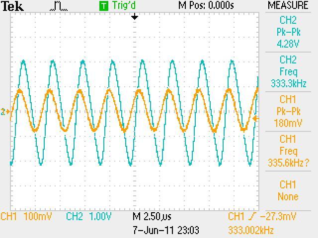
25 4.28/.18 = ~3dB drop

26 Now we can use this information in the following equation: Rout is measured to be 5.1kΩ with an ohm meter. Parasitic capacitance of breadboard = ( )( ) = 93.62pF Transient analysis at 20kHz We can use transient analysis to see the estimate the slew rate of the amplifier. The slew rate is the maximum rate of change of voltage at the output of the amplifier. The capacitance to ground is what causes slew rate limitations. So, for a maximum rate of change of the output voltage for an input signal: Slew Rate SR = At 20kHz the simulation shows a slew rate of 0 which doesn t take into consideration any parasitic capacitances.

27 Simulation slew At 20kHz the actual circuit shows a slew rate of = Conclusion After the amplifier has been built and tested it has met the specifications. A circuit simulator is an excellent tool but the limitations of it should be kept in mind. Circuit simulators work well with ideal conditions. However, ideal is a limit that can only be approached but not reached in an actual implementation. This is why with precise parameters, a circuit would need to be fine-tuned on the bench while being tested. This is due to inherent tolerances that naturally exist. The audio amplifier was an exciting project and only represents one of many applications of semiconductor technology.
Final Design Project: Variable Gain Amplifier with Output Stage Optimization for Audio Amplifier Applications EE 332: Summer 2011 Group 2: Chaz
 Final Design Project: Variable Gain Amplifier with Output Stage Optimization for Audio Amplifier Applications EE 332: Summer 2011 Group 2: Chaz Bofferding, Serah Peterson, Eric Stephanson, Casey Wojcik
A 3-STAGE 5W AUDIO AMPLIFIER
 ECE 2201 PRELAB 7x BJT APPLICATIONS A 3-STAGE 5W AUDIO AMPLIFIER UTILIZING NEGATIVE FEEDBACK INTRODUCTION Figure P7-1 shows a simplified schematic of a 3-stage audio amplifier utilizing three BJT amplifier
Experiment No. 9 DESIGN AND CHARACTERISTICS OF COMMON BASE AND COMMON COLLECTOR AMPLIFIERS
 Experiment No. 9 DESIGN AND CHARACTERISTICS OF COMMON BASE AND COMMON COLLECTOR AMPLIFIERS 1. Objective: The objective of this experiment is to explore the basic applications of the bipolar junction transistor
Homework Assignment 12
 Homework Assignment 12 Question 1 Shown the is Bode plot of the magnitude of the gain transfer function of a constant GBP amplifier. By how much will the amplifier delay a sine wave with the following
UNIVERSITY OF PENNSYLVANIA EE 206
 UNIVERSITY OF PENNSYLVANIA EE 206 TRANSISTOR BIASING CIRCUITS Introduction: One of the most critical considerations in the design of transistor amplifier stages is the ability of the circuit to maintain
Lab 2: Discrete BJT Op-Amps (Part I)
") Lab 2: Discrete BJT Op-Amps (Part I) This is a three-week laboratory. You are required to write only one lab report for all parts of this experiment. 1.0. INTRODUCTION In this lab, we will introduce and
Lab 2: Discrete BJT Op-Amps (Part I) This is a three-week laboratory. You are required to write only one lab report for all parts of this experiment. 1.0. INTRODUCTION In this lab, we will introduce and
Experiment 6: Biasing Circuitry
 1 Objective UNIVERSITY OF CALIFORNIA AT BERKELEY College of Engineering Department of Electrical Engineering and Computer Sciences EE105 Lab Experiments Experiment 6: Biasing Circuitry Setting up a biasing
Page 1 of 7. Power_AmpFal17 11/7/ :14
 ECE 3274 Power Amplifier Project (Push Pull) Richard Cooper 1. Objective This project will introduce two common power amplifier topologies, and also illustrate the difference between a Class-B and a Class-AB
CHARACTERIZATION OF OP-AMP
 EXPERIMENT 4 CHARACTERIZATION OF OP-AMP OBJECTIVES 1. To sketch and briefly explain an operational amplifier circuit symbol and identify all terminals. 2. To list the amplifier stages in a typical op-amp
Experiment 6: Biasing Circuitry
 1 Objective UNIVERSITY OF CALIFORNIA AT BERKELEY College of Engineering Department of Electrical Engineering and Computer Sciences EE105 Lab Experiments Experiment 6: Biasing Circuitry Setting up a biasing
AN-1106 Custom Instrumentation Amplifier Design Author: Craig Cary Date: January 16, 2017
 AN-1106 Custom Instrumentation Author: Craig Cary Date: January 16, 2017 Abstract This application note describes some of the fine points of designing an instrumentation amplifier with op-amps. We will
Using LME49810 to Build a High-Performance Power Amplifier Part I
 Using LME49810 to Build a High-Performance Power Amplifier Part I Panson Poon Introduction Although switching or Class-D amplifiers are gaining acceptance to audiophile community, linear amplification
Analog Integrated Circuit Configurations
 Analog Integrated Circuit Configurations Basic stages: differential pairs, current biasing, mirrors, etc. Approximate analysis for initial design MOSFET and Bipolar circuits Basic Current Bias Sources
LM13600 Dual Operational Transconductance Amplifiers with Linearizing Diodes and Buffers
 LM13600 Dual Operational Transconductance Amplifiers with Linearizing Diodes and Buffers General Description The LM13600 series consists of two current controlled transconductance amplifiers each with
THE HONG KONG POLYTECHNIC UNIVERSITY EN107/1 Department of Electronic and Information Engineering. EN107: OCL Class AB Power Amplifier Objective
 THE HONG KONG POLYTECHNIC UNIVERSITY EN107/1 EN107: OCL Class AB Power Amplifier Objective 1. To study the circuit performance of an OCL amplifier. 2. To study the effects of biasing on cross-over distortion
ECEN 325 Lab 5: Operational Amplifiers Part III
 ECEN Lab : Operational Amplifiers Part III Objectives The purpose of the lab is to study some of the opamp configurations commonly found in practical applications and also investigate the non-idealities
DEPARTMENT OF ELECTRICAL ENGINEERING AND COMPUTER SCIENCE MASSACHUSETTS INSTITUTE OF TECHNOLOGY CAMBRIDGE, MASSACHUSETTS 02139
 DEPARTMENT OF ELECTRICAL ENGINEERING AND COMPUTER SCIENCE MASSACHUSETTS INSTITUTE OF TECHNOLOGY CAMBRIDGE, MASSACHUSETTS 019.101 Introductory Analog Electronics Laboratory Laboratory No. READING ASSIGNMENT
Common-Source Amplifiers
 Lab 2: Common-Source Amplifiers Introduction The common-source stage is the most basic amplifier stage encountered in CMOS analog circuits. Because of its very high input impedance, moderate-to-high gain,
Midterm 2 Exam. Max: 90 Points
 Midterm 2 Exam Name: Max: 90 Points Question 1 Consider the circuit below. The duty cycle and frequency of the 555 astable is 55% and 5 khz respectively. (a) Determine a value for so that the average current
Page 1. Telecommunication Electronics ETLCE - A2 06/09/ DDC 1. Politecnico di Torino ICT School. Amplifiers
 Politecnico di Torino ICT School Amplifiers Telecommunication Electronics A2 Transistor amplifiers» Bias point and circuits,» Small signal models» Gain and bandwidth» Limits of linear analysis Op Amp amplifiers
Chip Name Min VolT. Max Volt. Min. Out Power Typ. Out Power. LM386N-1 4 Volts 12 Volts 250 mw 325 mw. LM386N-3 4 Volts 12 Volts 500 mw 700 mw
 LM386 Audio Amplifier Analysis The LM386 Voltage Audio Power Amplifier by National Semiconductor and also manufactured by JRC/NJM, is an old chip (mid 70 s) that has been a popular choice for low-power
Figure 1. Block diagram of system incorporating power amplification.
 It is often necessary use a circuit which has very low power capabilities to drive a system which has relatively high power requirements. This is typically accomplished by using an amplifier as an intermediate
Designing an Audio Amplifier Using a Class B Push-Pull Output Stage
 Designing an Audio Amplifier Using a Class B Push-Pull Output Stage Angel Zhang Electrical Engineering The Cooper Union for the Advancement of Science and Art Manhattan, NY Jeffrey Shih Electrical Engineering
55:041 Electronic Circuits The University of Iowa Fall Exam 3. Question 1 Unless stated otherwise, each question below is 1 point.
 Exam 3 Name: Score /65 Question 1 Unless stated otherwise, each question below is 1 point. 1. An engineer designs a class-ab amplifier to deliver 2 W (sinusoidal) signal power to an resistive load. Ignoring
EE 330 Laboratory 8 Discrete Semiconductor Amplifiers
 EE 330 Laboratory 8 Discrete Semiconductor Amplifiers Fall 2017 Contents Objective:... 2 Discussion:... 2 Components Needed:... 2 Part 1 Voltage Controlled Amplifier... 2 Part 2 Common Source Amplifier...
Lab 2: Common Base Common Collector Design Exercise
 CSUS EEE 109 Lab - Section 01 Lab 2: Common Base Common Collector Design Exercise Author: Bogdan Pishtoy / Lab Partner: Roman Vermenchuk Lab Report due March 26 th Lab Instructor: Dr. Kevin Geoghegan 2016-03-25
EE 330 Laboratory 8 Discrete Semiconductor Amplifiers
 EE 330 Laboratory 8 Discrete Semiconductor Amplifiers Fall 2018 Contents Objective:...2 Discussion:...2 Components Needed:...2 Part 1 Voltage Controlled Amplifier...2 Part 2 A Nonlinear Application...3
Lecture (06) BJT Amplifiers 3
 BJT Amplifiers 3") Lecture (06) BJT Amplifiers 3 By: Dr. Ahmed ElShafee 1 Current Gain 2 Power Gain The overall power gain is the product of the overall voltage gain (Av ) and the overall current gain (Ai). 3 THE COMMON
Lecture (06) BJT Amplifiers 3 By: Dr. Ahmed ElShafee 1 Current Gain 2 Power Gain The overall power gain is the product of the overall voltage gain (Av ) and the overall current gain (Ai). 3 THE COMMON
Final Project Stereo Audio Amplifier Final Report
 The George Washington University School of Engineering and Applied Science Department of Electrical and Computer Engineering Final Project Stereo Audio Amplifier Final Report Daniel S. Boucher ECE 20-32,
ECE 3274 Common-Emitter Amplifier Project
 ECE 3274 Common-Emitter Amplifier Project 1. Objective The objective of this lab is to design and build three variations of the common- emitter amplifier. 2. Components Qty Device 1 2N2222 BJT Transistor
DEPARTMENT OF ELECTRICAL ENGINEERING AND COMPUTER SCIENCE MASSACHUSETTS INSTITUTE OF TECHNOLOGY CAMBRIDGE, MASSACHUSETTS 02139
 DEPARTMENT OF ELECTRICAL ENGINEERING AND COMPUTER SCIENCE MASSACHUSETTS INSTITUTE OF TECHNOLOGY CAMBRIDGE, MASSACHUSETTS 019 Spring Term 00.101 Introductory Analog Electronics Laboratory Laboratory No.
5.25Chapter V Problem Set
 5.25Chapter V Problem Set P5.1 Analyze the circuits in Fig. P5.1 and determine the base, collector, and emitter currents of the BJTs as well as the voltages at the base, collector, and emitter terminals.
Opamp Based Power Amplifier
 Introduction Opamp Based Power Amplifier Rohit Balkishan This is a contributed project from Rohit Balkishan, who has built it, and thought that it would make a nice simple project for others. This is a
A 7ns, 6mA, Single-Supply Comparator Fabricated on Linear s 6GHz Complementary Bipolar Process
 A 7ns, 6mA, Single-Supply Comparator Fabricated on Linear s 6GHz Complementary Bipolar Process Introduction The is an ultrafast (7ns), low power (6mA), single-supply comparator designed to operate on either
Linear electronic. Lecture No. 1
 1 Lecture No. 1 2 3 4 5 Lecture No. 2 6 7 8 9 10 11 Lecture No. 3 12 13 14 Lecture No. 4 Example: find Frequency response analysis for the circuit shown in figure below. Where R S =4kR B1 =8kR B2 =4k R
Low Distortion Design 3
 Low Distortion Design 3 TIPL 1323 TI Precision Labs Op Amps Presented by Collin Wells Prepared by John Caldwell Prerequisites: Noise 1 3 (TIPL1311 TIPL1313) Output Stage Topologies Most op amps use a Class-AB
Experiment 9- Single Stage Amplifiers with Passive Loads - MOS
 Experiment 9- Single Stage Amplifiers with Passive oads - MOS D. Yee,.T. Yeung, M. Yang, S.M. Mehta, and R.T. Howe UC Berkeley EE 105 1.0 Objective This is the second part of the single stage amplifier
Unit WorkBook 1 Level 4 ENG U22 Electronic Circuits and Devices 2018 UniCourse Ltd. All Rights Reserved. Sample
 Pearson BTEC Level 4 Higher Nationals in Engineering (RQF) Unit 22: Electronic Circuits and Devices Unit Workbook 1 in a series of 4 for this unit Learning Outcome 1 Operational Amplifiers Page 1 of 23
Operational Amplifier BME 360 Lecture Notes Ying Sun
 Operational Amplifier BME 360 Lecture Notes Ying Sun Characteristics of Op-Amp An operational amplifier (op-amp) is an analog integrated circuit that consists of several stages of transistor amplification
ECEN 325 Lab 7: Characterization and DC Biasing of the BJT
 ECEN 325 Lab 7: Characterization and DC Biasing of the BJT 1 Objectives The purpose of this lab is to characterize NPN and PNP bipolar junction transistors (BJT), and to analyze and design DC biasing circuits
Solid State Devices & Circuits. 18. Advanced Techniques
 ECE 442 Solid State Devices & Circuits 18. Advanced Techniques Jose E. Schutt-Aine Electrical l&c Computer Engineering i University of Illinois jschutt@emlab.uiuc.edu 1 Darlington Configuration - Popular
University of Michigan EECS 311: Electronic Circuits Fall 2008 LAB 4 SINGLE STAGE AMPLIFIER
 University of Michigan EECS 311: Electronic Circuits Fall 2008 LAB 4 SINGLE STAGE AMPLIFIER Issued 10/27/2008 Report due in Lecture 11/10/2008 Introduction In this lab you will characterize a 2N3904 NPN
Audio Power Amplifiers with Feedback Linearization
 Lab 5: Audio Power Amplifiers with Feedback Linearization Introduction The Power Amplifier (PA) is one of the most important circuits in modern electronics. Critical aspects of PA operation are its output
Unit WorkBook 4 Level 4 ENG U19 Electrical and Electronic Principles LO4 Digital & Analogue Electronics 2018 Unicourse Ltd. All Rights Reserved.
 Pearson BTEC Levels 4 Higher Nationals in Engineering (RQF) Unit 19: Electrical and Electronic Principles Unit Workbook 4 in a series of 4 for this unit Learning Outcome 4 Digital & Analogue Electronics
In a cascade configuration, the overall voltage and current gains are given by:
 ECE 3274 Two-Stage Amplifier Project 1. Objective The objective of this lab is to design and build a direct coupled two-stage amplifier, including a common-source gain stage and a common-collector buffer
Code No: R Set No. 1
 Code No: R059210404 Set No. 1 II B.Tech I Semester Supplimentary Examinations, February 2008 ELECTRONIC CIRCUIT ANALYSIS ( Common to Electronics & Communication Engineering and Electronics & Telematics)
Boosting output in high-voltage op-amps with a current buffer
 Boosting output in high-voltage op-amps with a current buffer Author: Joe Kyriakakis, Apex Microtechnology Date: 02/18/2014 Categories: Current, Design Tools, High Voltage, MOSFETs & Power MOSFETs, Op
Well we know that the battery Vcc must be 9V, so that is taken care of.
 HW 4 For the following problems assume a 9Volt battery available. 1. (50 points, BJT CE design) a) Design a common emitter amplifier using a 2N3904 transistor for a voltage gain of Av=-10 with the collector
Miniproject: AM Radio
 Objective UNIVERSITY OF CALIFORNIA AT BERKELEY College of Engineering Department of Electrical Engineering and Computer Sciences EE05 Lab Experiments Miniproject: AM Radio Until now, the labs have focused
ECE 310L : LAB 9. Fall 2012 (Hay)
") ECE 310L : LAB 9 PRELAB ASSIGNMENT: Read the lab assignment in its entirety. 1. For the circuit shown in Figure 3, compute a value for R1 that will result in a 1N5230B zener diode current of approximately
ECE 310L : LAB 9 PRELAB ASSIGNMENT: Read the lab assignment in its entirety. 1. For the circuit shown in Figure 3, compute a value for R1 that will result in a 1N5230B zener diode current of approximately
The B7 Discrete Operational Amplifier Author: Tamas G. Kohalmi 7/5/2004
 The B7 Discrete Operational Amplifier Author: Tamas G. Kohalmi 7/5/2004 Table of Contents Part 1... pages 2-4 Part 2 pages 5-7 Part 1. This document describes a simple discrete operational amplifier that
ECEN Network Analysis Section 3. Laboratory Manual
 ECEN 3714----Network Analysis Section 3 Laboratory Manual LAB 07: Active Low Pass Filter Oklahoma State University School of Electrical and Computer Engineering. Section 3 Laboratory manual - 1 - Spring
Final Project Report Stereo Audio Amplifier
 The George Washington University School Of Engineering And Applied Science Department Of Electrical And Computer Engineering Final Project Report Stereo Audio Amplifier By Ben Ruppel 145-82-8718 ECE 20-32
Electronics Lab. (EE21338)
") Princess Sumaya University for Technology The King Abdullah II School for Engineering Electrical Engineering Department Electronics Lab. (EE21338) Prepared By: Eng. Eyad Al-Kouz October, 2012 Table of
Princess Sumaya University for Technology The King Abdullah II School for Engineering Electrical Engineering Department Electronics Lab. (EE21338) Prepared By: Eng. Eyad Al-Kouz October, 2012 Table of
ENEE 307 Electronic Circuit Design Laboratory Spring A. Iliadis Electrical Engineering Department University of Maryland College Park MD 20742
 ENEE 307 Electronic Circuit Design Laboratory Spring 2012 A. Iliadis Electrical Engineering Department University of Maryland College Park MD 20742 Video Amps 2.2. Video Amplifiers Before coming to this
For the purpose of this problem sheet use the model given in the lecture notes.
 Analogue Electronics Questions Todd Huffman & Tony Weidberg, MT 2018 (updated 30/10/18). For the purpose of this problem sheet use the model given in the lecture notes. The current gain is defined by a
Op Amp Booster Designs
 Op Amp Booster Designs Although modern integrated circuit operational amplifiers ease linear circuit design, IC processing limits amplifier output power. Many applications, however, require substantially
Audio Amplifier. November 27, 2017
 Audio Amplifier November 27, 2017 1 Pre-lab No pre-lab calculations. 2 Introduction In this lab, you will build an audio power amplifier capable of driving a 8 Ω speaker the way it was meant to be driven...
Operational Amplifiers
 Operational Amplifiers Table of contents 1. Design 1.1. The Differential Amplifier 1.2. Level Shifter 1.3. Power Amplifier 2. Characteristics 3. The Opamp without NFB 4. Linear Amplifiers 4.1. The Non-Inverting
Linear IC s and applications
 Questions and Solutions PART-A Unit-1 INTRODUCTION TO OP-AMPS 1. Explain data acquisition system Jan13 DATA ACQUISITION SYSYTEM BLOCK DIAGRAM: Input stage Intermediate stage Level shifting stage Output
Common-source Amplifiers
 Lab 1: Common-source Amplifiers Introduction The common-source amplifier is one of the basic amplifiers in CMOS analog circuits. Because of its very high input impedance, relatively high gain, low noise,
ECE 454 Homework #1 Due 11/28/2018 This Wednesday In Lab
 ECE 454 Homework #1 Due 11/28/2018 This Wednesday In Lab Design the Darlington push-pull amplifier specified in Lab 1: You will build this amplifier for Lab 1 so use parts that are available in the lab.
LM13700 Dual Operational Transconductance Amplifiers with Linearizing Diodes and Buffers
 LM13700 Dual Operational Transconductance Amplifiers with Linearizing Diodes and Buffers General Description The LM13700 series consists of two current controlled transconductance amplifiers, each with
SIDDHARTH GROUP OF INSTITUTIONS :: PUTTUR (AUTONOMOUS) Siddharth Nagar, Narayanavanam Road QUESTION BANK
 Siddharth Nagar, Narayanavanam Road QUESTION BANK") SIDDHARTH GROUP OF INSTITUTIONS :: PUTTUR (AUTONOMOUS) Siddharth Nagar, Narayanavanam Road 517583 QUESTION BANK Subject with Code : Electronic Circuit Analysis (16EC407) Year & Sem: II-B.Tech & II-Sem
SIDDHARTH GROUP OF INSTITUTIONS :: PUTTUR (AUTONOMOUS) Siddharth Nagar, Narayanavanam Road 517583 QUESTION BANK Subject with Code : Electronic Circuit Analysis (16EC407) Year & Sem: II-B.Tech & II-Sem
EE12: Laboratory Project (Part-2) AM Transmitter
 AM Transmitter") EE12: Laboratory Project (Part-2) AM Transmitter ECE Department, Tufts University Spring 2008 1 Objective This laboratory exercise is the second part of the EE12 project of building an AM transmitter in
EE12: Laboratory Project (Part-2) AM Transmitter ECE Department, Tufts University Spring 2008 1 Objective This laboratory exercise is the second part of the EE12 project of building an AM transmitter in
Field Effect Transistors
 Field Effect Transistors Purpose In this experiment we introduce field effect transistors (FETs). We will measure the output characteristics of a FET, and then construct a common-source amplifier stage,
BJT Differential Amplifiers
 Instituto Tecnológico y de Estudios Superiores de Occidente (), OBJECTIVES The general objective of this experiment is to contrast the practical behavior of a real differential pair with its theoretical
BJT Circuits (MCQs of Moderate Complexity)
") BJT Circuits (MCQs of Moderate Complexity) 1. The current ib through base of a silicon npn transistor is 1+0.1 cos (1000πt) ma. At 300K, the rπ in the small signal model of the transistor is i b B C r
BJT Circuits (MCQs of Moderate Complexity) 1. The current ib through base of a silicon npn transistor is 1+0.1 cos (1000πt) ma. At 300K, the rπ in the small signal model of the transistor is i b B C r
PHYS225 Lecture 6. Electronic Circuits
 PHYS225 Lecture 6 Electronic Circuits Transistors History Basic physics of operation Ebers-Moll model Small signal equivalent Last lecture Introduction to Transistors A transistor is a device with three
PartIIILectures. Multistage Amplifiers
 University of missan Electronic II, Second year 2015-2016 PartIIILectures Assistant Lecture: 1 Multistage and Compound Amplifiers Basic Definitions: 1- Gain of Multistage Amplifier: Fig.(1-1) A general
EE301 Electronics I , Fall
 EE301 Electronics I 2018-2019, Fall 1. Introduction to Microelectronics (1 Week/3 Hrs.) Introduction, Historical Background, Basic Consepts 2. Rewiev of Semiconductors (1 Week/3 Hrs.) Semiconductor materials
LM13700 Dual Operational Transconductance Amplifiers with Linearizing Diodes and Buffers
 LM13700 Dual Operational Transconductance Amplifiers with Linearizing Diodes and Buffers General Description The LM13700 series consists of two current controlled transconductance amplifiers, each with
University of Pittsburgh
 University of Pittsburgh Experiment #1 Lab Report Frequency Response of Operational Amplifiers Submission Date: 05/29/2018 Instructors: Dr. Ahmed Dallal Shangqian Gao Submitted By: Nick Haver & Alex Williams
University of North Carolina, Charlotte Department of Electrical and Computer Engineering ECGR 3157 EE Design II Fall 2009
 University of North Carolina, Charlotte Department of Electrical and Computer Engineering ECGR 3157 EE Design II Fall 2009 Lab 1 Power Amplifier Circuits Issued August 25, 2009 Due: September 11, 2009
LABORATORY #3 QUARTZ CRYSTAL OSCILLATOR DESIGN
 LABORATORY #3 QUARTZ CRYSTAL OSCILLATOR DESIGN OBJECTIVES 1. To design and DC bias the JFET transistor oscillator for a 9.545 MHz sinusoidal signal. 2. To simulate JFET transistor oscillator using MicroCap
LM148/LM248/LM348 Quad 741 Op Amps
 Quad 741 Op Amps General Description The LM148 series is a true quad 741. It consists of four independent, high gain, internally compensated, low power operational amplifiers which have been designed to
Objectives The purpose of this lab is build and analyze Differential amplifier based on NPN transistors.
 1 Lab 03: Differential Amplifier Total 30 points: 20 points for lab, 5 points for well-organized report, 5 points for immaculate circuit on breadboard NOTES: 1) Please use the basic current mirror from
EE 501 Lab 10 Output Amplifier Due: December 10th, 2015
 EE 501 Lab 10 Output Amplifier Due: December 10th, 2015 Objective: Get familiar with output amplifier. Design an output amplifier driving small resistor load. Design an output amplifier driving large capacitive
EE 3305 Lab I Revised July 18, 2003
 Operational Amplifiers Operational amplifiers are high-gain amplifiers with a similar general description typified by the most famous example, the LM741. The LM741 is used for many amplifier varieties
ECE4902 C Lab 5 MOSFET Common Source Amplifier with Active Load Bandwidth of MOSFET Common Source Amplifier: Resistive Load / Active Load
 ECE4902 C2012 - Lab 5 MOSFET Common Source Amplifier with Active Load Bandwidth of MOSFET Common Source Amplifier: Resistive Load / Active Load PURPOSE: The primary purpose of this lab is to measure the
UNIVERSITY OF UTAH ELECTRICAL ENGINEERING DEPARTMENT
 UNIVERSITY OF UTAH ELECTRICAL ENGINEERING DEPARTMENT ECE 3110 LAB EXPERIMENT NO. 4 CLASS AB POWER OUTPUT STAGE Objective: In this laboratory exercise you will build and characterize a class AB power output
Başkent University Department of Electrical and Electronics Engineering EEM 214 Electronics I Experiment 9
 Başkent University Department of Electrical and Electronics Engineering EEM 214 Electronics I Experiment 9 COMMON-COLLECTOR (EMITTER FOLLOWER) AMPLIFIER Aim: 1. To measure the open-circuit voltage gain,
UNIVERSITY OF NORTH CAROLINA AT CHARLOTTE Department of Electrical and Computer Engineering
 UNIVERSITY OF NORTH CAROLINA AT CHARLOTTE Department of Electrical and Computer Engineering EXPERIMENT 8 MOSFET AMPLIFIER CONFIGURATIONS AND INPUT/OUTPUT IMPEDANCE OBJECTIVES The purpose of this experiment
Exercise 2: AC Voltage and Power Gains
 Exercise 2: AC Voltage and Power Gains When you have completed this exercise, you will be able to determine voltage and power gains by using oscilloscope. The ac operation schematic for the COMPLEMENTARY
I1 19u 5V R11 1MEG IDC Q7 Q2N3904 Q2N3904. Figure 3.1 A scaled down 741 op amp used in this lab
 Lab 3: 74 Op amp Purpose: The purpose of this laboratory is to become familiar with a two stage operational amplifier (op amp). Students will analyze the circuit manually and compare the results with SPICE.
Oscillators. An oscillator may be described as a source of alternating voltage. It is different than amplifier.
 Oscillators An oscillator may be described as a source of alternating voltage. It is different than amplifier. An amplifier delivers an output signal whose waveform corresponds to the input signal but
Integrators, differentiators, and simple filters
 BEE 233 Laboratory-4 Integrators, differentiators, and simple filters 1. Objectives Analyze and measure characteristics of circuits built with opamps. Design and test circuits with opamps. Plot gain vs.
School of Sciences. ELECTRONICS II ECE212A 2 nd Assignment
 School of Sciences SPRING SEMESTER 2010 INSTRUCTOR: Dr Konstantinos Katzis COURSE / SECTION: ECE212N COURSE TITLE: Electronics II OFFICE RM#: 124 (1 st floor) OFFICE TEL#: 22713296 OFFICE HOURS: Monday
Figure 2 shows the actual schematic for the power supply and one channel.
 Pass Laboratories Aleph 3 Service Manual rev 0 2/1/96 Aleph 3 Service Manual. The Aleph 3 is a stereo 30 watt per channel audio power amplifier which operates in single-ended class A mode. The Aleph 3
DEPARTMENT OF ELECTRICAL ENGINEERING AND COMPUTER SCIENCE MASSACHUSETTS INSTITUTE OF TECHNOLOGY CAMBRIDGE, MASSACHUSETTS 02139
 DEPARTMENT OF ELECTRICAL ENGINEERING AND COMPUTER SCIENCE MASSACHUSETTS INSTITUTE OF TECHNOLOGY CAMBRIDGE, MASSACHUSETTS 02139 Spring Term 2007 6.101 Introductory Analog Electronics Laboratory Laboratory
EXPERIMENT 5 CURRENT AND VOLTAGE CHARACTERISTICS OF BJT
 EXPERIMENT 5 CURRENT AND VOLTAGE CHARACTERISTICS OF BJT 1. OBJECTIVES 1.1 To practice how to test NPN and PNP transistors using multimeter. 1.2 To demonstrate the relationship between collector current
Lab 5: Multi-Stage Amplifiers
 UNIVERSITY OF CALIFORNIA AT BERKELEY College of Engineering Department of Electrical Engineering and Computer Sciences EE105 Lab Experiments Lab 5: Multi-Stage Amplifiers Contents 1 Introduction 1 2 Pre-Lab
The Aleph 2 is a monoblock 100 watt audio power amplifier which operates in single-ended class A mode.
 Pass Laboratories Aleph 2 Service Manual Rev 0 2/1/96 Aleph 2 Service Manual. The Aleph 2 is a monoblock 100 watt audio power amplifier which operates in single-ended class A mode. The Aleph 2 has only
2. SINGLE STAGE BIPOLAR JUNCTION TRANSISTOR (BJT) AMPLIFIERS
 AMPLIFIERS") 2. SINGLE STAGE BIPOLAR JUNCTION TRANSISTOR (BJT) AMPLIFIERS I. Objectives and Contents The goal of this experiment is to become familiar with BJT as an amplifier and to evaluate the basic configurations
2. SINGLE STAGE BIPOLAR JUNCTION TRANSISTOR (BJT) AMPLIFIERS I. Objectives and Contents The goal of this experiment is to become familiar with BJT as an amplifier and to evaluate the basic configurations
Radivoje Đurić, 2015, Analogna Integrisana Kola 1
 OTA-output buffer 1 According to the types of loads, the driving capability of the output stages differs. For switched capacitor circuits which have high impedance capacitive loads, class A output stage
Analog Integrated Circuit Design Exercise 1
 Analog Integrated Circuit Design Exercise 1 Integrated Electronic Systems Lab Prof. Dr.-Ing. Klaus Hofmann M.Sc. Katrin Hirmer, M.Sc. Sreekesh Lakshminarayanan Status: 21.10.2015 Pre-Assignments The lecture
Laboratory 4 Operational Amplifier Department of Mechanical and Aerospace Engineering University of California, San Diego MAE170
 Laboratory 4 Operational Amplifier Department of Mechanical and Aerospace Engineering University of California, San Diego MAE170 Megan Ong Diana Wu Wong B01 Tuesday 11am April 28 st, 2015 Abstract: The
The Aleph 5 is a stereo 60 watt audio power amplifier which operates in single-ended class A mode.
 Pass Laboratories Aleph 5 Service Manual Rev 0 9/20/96 Aleph 5 Service Manual. The Aleph 5 is a stereo 60 watt audio power amplifier which operates in single-ended class A mode. The Aleph 5 has only two
 EC 6411 CIRCUITS AND SIMULATION INTEGRATED LABORATORY LABORATORY MANUAL INDEX EXPT.NO NAME OF THE EXPERIMENT PAGE NO 1 HALF WAVE AND FULL WAVE RECTIFIER 3 2 FIXED BIAS AMPLIFIER CIRCUIT USING BJT 3 BJT
TDA W Hi-Fi AUDIO POWER AMPLIFIER
 32W Hi-Fi AUDIO POWER AMPLIFIER HIGH OUTPUT POWER (50W MUSIC POWER IEC 268.3 RULES) HIGH OPERATING SUPPLY VOLTAGE (50V) SINGLE OR SPLIT SUPPLY OPERATIONS VERY LOW DISTORTION SHORT CIRCUIT PROTECTION (OUT