|
|
|
- Charles Hodges
- 5 years ago
- Views:
Transcription

1 An ISO 9001:2008 Certified Institution EC6501-Digital Communication 1
2 Unit-1: Sampling & Quantization The purpose of a Communication System is to transport an information bearing signal from a source to a user destination via a communication channel. MODEL OF A COMMUNICATION SYSTEM(ANALOG) Information Source and Input I/P Signal TRANSMITTER CHANNEL Destination and Output Transducer O/P Signal RECEIVER Fig. 1.1: Block diagram of Communication System. The three basic elements of every communication systems are Transmitter, Receiver and Channel. The Overall purpose of this system is to transfer information from one point (called Source) to another point, the user destination. The message produced by a source, normally, is not electrical. Hence an input transducer is used for converting the message to a time varying electrical quantity called message signal. Similarly, at the destination point, another transducer converts the electrical waveform to the appropriate message. The transmitter is located at one point in space, the receiver is located at some other point separate from the transmitter, and the channel is the medium that provides the electrical connection between them. The purpose of the transmitter is to transform the message signal produced by the source of information into a form suitable for transmission over the channel. The received signal is normally corrupted version of the transmitted signal, which is due to channel imperfections, noise and interference from other sources.the receiver has the task of operating on the received signal so 2
3 as to reconstruct a recognizable form of the original message signal and to deliver it to the user destination. Communication Systems are divided into 3 categories: 1. Analog Communication Systems are designed to transmit analog information using analog modulation methods. 2. Digital Communication Systems are designed for transmitting digital information using digital modulation schemes, and 3. Hybrid Systems that use digital modulation schemes for transmitting sampled and quantized values of an analog message signal. ELEMENTS OF DIGITAL COMMUNICATION SYSTEMS: The figure 1.2 shows the functional elements of a digital communication system. Source of Information: 1. Analog Information Sources. 2. Digital Information Sources. Analog Information Sources Microphone actuated by a speech, TV Camera scanning a scene, continuous amplitude signals. Digital Information Sources These are teletype or the numerical output of computer which consists of a sequence of discrete symbols or letters. An Analog information is transformed into a discrete information through the process of sampling and quantizing. Digital Communication System Source of Information Source Encoder Channel Encoder Modulator Channel Received Signal User of Information Source Decoder Channel Decoder Demodulator 3
4 Fig 1.2: Block Diagram of a Digital Communication System SOURCE ENCODER / DECODER: The Source encoder ( or Source coder) converts the input i.e. symbol sequence into a binary sequence of 0 s and 1 s by assigning code words to the symbols in the input sequence. For eg. :-If a source set is having hundred symbols, then the number of bits used to represent each symbol will be 7 because 2 7 =128 unique combinations are available. The important parameters of a source encoder are block size, code word lengths, average data rate and the efficiency of the coder (i.e. actual output data rate compared to the minimum achievable rate) At the receiver, the source decoder converts the binary output of the channel decoder into a symbol sequence. The decoder for a system using fixed length code words is quite simple, but the decoder for a system using variable length code words will be very complex. Aim of the source coding is to remove the redundancy in the transmitting information, so that bandwidth required for transmission is minimized. Based on the probability of the symbol code word is assigned. Higher the probability, shorter is the codeword. Ex: Huffman coding. CHANNEL ENCODER / DECODER: Error control is accomplished by the channel coding operation that consists of systematically adding extra bits to the output of the source coder. These extra bits do not convey any information but helps the receiver to detect and / or correct some of the errors in the information bearing bits. There are two methods of channel coding: 1. Block Coding: The encoder takes a block of k information bits from the source encoder and adds r error control bits, where r is dependent on k and error control capabilities desired. 2. Convolution Coding: The information bearing message stream is encoded in a continuous fashion by continuously interleaving information bits and error control bits. 4
5 The Channel decoder recovers the information bearing bits from the coded binary stream. Error detection and possible correction is also performed by the channel decoder. The important parameters of coder / decoder are: Method of coding, efficiency, error control capabilities and complexity of the circuit. MODULATOR: The Modulator converts the input bit stream into an electrical waveform suitable for transmission over the communication channel. Modulator can be effectively used to minimize the effects of channel noise, to match the frequency spectrum of transmitted signal with channel characteristics, to provide the capability to multiplex many signals. DEMODULATOR: The extraction of the message from the information bearing waveform produced by the modulation is accomplished by the demodulator. The output of the demodulator is bit stream. The important parameter is the method of demodulation. CHANNEL: The Channel provides the electrical connection between the source and destination. The different channels are: Pair of wires, Coaxial cable, Optical fibre, Radio channel, Satellite channel or combination of any of these. The communication channels have only finite Bandwidth, non-ideal frequency response, the signal often suffers amplitude and phase distortion as it travels over the channel. Also, the signal power decreases due to the attenuation of the channel. The signal is corrupted by unwanted, unpredictable electrical signals referred to as noise. The important parameters of the channel are Signal to Noise power Ratio (SNR), usable bandwidth, amplitude and phase response and the statistical properties of noise. Advantages of Digital Communication 1. The effect of distortion, noise and interference is less in a digital communication system. This is because the disturbance must be large enough to change the pulse from one state to the other. 5
6 2. Regenerative repeaters can be used at fixed distance along the link, to identify and regenerate a pulse before it is degraded to an ambiguous state. 3. Digital circuits are more reliable and cheaper compared to analog circuits. 4. The Hardware implementation is more flexible than analog hardware because of the use of microprocessors, VLSI chips etc. 5. Signal processing functions like encryption, compression can be employed to maintain the secrecy of the information. 6. Error detecting and Error correcting codes improve the system performance by reducing the probability of error. 7. Combining digital signals using TDM is simpler than combining analog signals using FDM. The different types of signals such as data, telephone, TV can be treated as identical signals in transmission and switching in a digital communication system. 8. We can avoid signal jamming using spread spectrum technique. Disadvantages of Digital Communication: 1. Large System Bandwidth:- Digital transmission requires a large system bandwidth to communicate the same information in a digital format as compared to analog format. 2. System Synchronization:- Digital detection requires system synchronization whereas the analog signals generally have no such requirement. Channels for Digital Communications The modulation and coding used in a digital communication system depend on the characteristics of the channel. The two main characteristics of the channel are BANDWIDTH and POWER. In addition the other characteristics are whether the channel is linear or nonlinear, and how free the channel is free from the external interference. 6
7 Five channels are considered in the digital communication, namely: telephone channels, coaxial cables, optical fibers, microwave radio, and satellite channels. Telephone channel: It is designed to provide voice grade communication. Also good for data communication over long distances. The channel has a band-pass characteristic occupying the frequency range 300Hz to 3400hz, a high SNR of about 30db, and approximately linear response. For the transmission of voice signals the channel provides flat amplitude response. But for the transmission of data and image transmissions, since the phase delay variations are important an equalizer is used to maintain the flat amplitude response and a linear phase response over the required frequency band. Transmission rates upto16.8 kilobits per second have been achieved over the telephone lines. Coaxial Cable: The coaxial cable consists of a single wire conductor centered inside an outer conductor, which is insulated from each other by a dielectric. The main advantages of the coaxial cable are wide bandwidth and low external interference. But closely spaced repeaters are required. With repeaters spaced at 1km intervals the data rates of 274 megabits per second have been achieved. Optical Fibers: An optical fiber consists of a very fine inner core made of silica glass, surrounded by a concentric layer called cladding that is also made of glass. The refractive index of the glass in the core is slightly higher than refractive index of the glass in the cladding. Hence if a ray of light is launched into an optical fiber at the right oblique acceptance angle, it is continually refracted into the core by the cladding. That means the difference between the refractive indices of the core and cladding helps guide the propagation of the ray of light inside the core of the fiber from one end to the other. Compared to coaxial cables, optical fibers are smaller in size and they offer higher transmission bandwidths and longer repeater separations. Microwave radio: A microwave radio, operating on the line-of-sight link, consists basically of a transmitter and a receiver that are equipped with antennas. The antennas are placed on towers at sufficient height to have the transmitter and receiver in line-of-sight of each other. The operating frequencies range from 1 to 30 GHz. 7
8 Under normal atmospheric conditions, a microwave radio channel is very reliable and provides path for high-speed digital transmission. But during meteorological variations, a severe degradation occurs in the system performance. Satellite Channel: A Satellite channel consists of a satellite in geostationary orbit, an uplink from ground station, and a down link to another ground station. Both link operate at microwave frequencies, with uplink the uplink frequency higher than the down link frequency. In general, Satellite can be viewed as repeater in the sky. It permits communication over long distances at higher bandwidths and relatively low cost. Bandwidth: Bandwidth is simply a measure of frequency range. The range of frequencies contained in a composite signal is its bandwidth. The bandwidth is normally a difference between two numbers. For example, if a composite signal contains frequencies between 1000 and 5000, its bandwidth is , or If a range of 2.40 GHz to 2.48 GHz is used by a device, then the bandwidth would be 0.08 GHz (or more commonly stated as 80MHz).It is easy to see that the bandwidth we define here is closely related to the amount of data you can transmit within it - the more room in frequency space, the more data you can fit in at a given moment. The term bandwidth is often used for something we should rather call a data rate, as in my Internet connection has 1 Mbps of bandwidth, meaning it can transmit data at 1 megabit per second. SAMPLING: A message signal may originate from a digital or analog source. If the message signal is analog in nature, then it has to be converted into digital form before it can transmitted by digital means. The process by which the continuous-time signal is converted into a discrete time signal is called Sampling. Sampling operation is performed in accordance with the sampling theorem. SAMPLING THEOREM FOR LOW-PASS SIGNALS:- Statement:- If a band limited signal g(t) contains no frequency components for f > W, 8
9 then it is completely described by instantaneous values g(kt s ) uniformly spaced in time with period T s 1/2W. If the sampling rate, fs is equal to the Nyquist rate or greater (fs 2W), the signal g(t) can be exactly reconstructed. g(t) s δ (t) -2Ts -Ts 0 1Ts 2Ts 3Ts 4Ts g δ (t) -2Ts -Ts 0 Ts 2Ts 3Ts 4Ts Fig : Sampling process 9
10 Proof:- Part - I If a signal x(t) does not contain any frequency component beyond W Hz, then the signal is completely described by its instantaneous uniform samples with sampling interval (or period ) of Ts < 1/(2W) sec. Part II The signal x(t) can be accurately reconstructed (recovered) from the set of uniform instantaneous samples by passing the samples sequentially through an ideal (brick-wall) lowpass filter with bandwidth B, where W B < fs W and fs = 1/(Ts). If x(t) represents a continuous-time signal, the equivalent set of instantaneous uniform samples {x(nts)} may be represented as, {x(nts)} xs(t) = Σ x(t).δ (t- nts) where x(nts) = x(t) t =nts, δ (t) is a unit pulse singularity function and n is an integer.the continuous-time signal x(t) is multiplied by an (ideal) impulse train to obtain {x(nts)} and can be rewritten as, xs(t) = x(t).σ δ (t- nts) Now, let X(f) denote the Fourier Transform F(T) of x(t), i.e Now, from the theory of Fourier Transform, we know that the F.T of Σ δ (t- nts), the impulse train in time domain, is an impulse train in frequency domain: F{Σ δ (t- nts)} = (1/Ts).Σ δ (f- n/ts) = fs.σ δ (f- nfs) If Xs(f) denotes the Fourier transform of the energy signal xs(t), we can write using Eq. (1.2.4) and the convolution property: Xs(f) = X(f)* F{Σ δ (t- nts)} = X(f)*[fs.Σ δ (f- nfs)] = fs.x(f)*σ δ (f- nfs) This equation, when interpreted appropriately, gives an intuitive proof to 10
11 Nyquist s theorems as stated above and also helps to appreciate their practical implications. Let us note that while writing Eq.(1.5), we assumed that x(t) is an energy signal so that its Fourier transform exists. With this setting, if we assume that x(t) has no appreciable frequency component greater than W Hz and if fs > 2W, then Eq.(1.5) implies that Xs(f), the Fourier Transform of the sampled signal xs(t) consists of infinite number of replicas of X(f), centered at discrete frequencies n.fs, - < n < and scaled by a constant fs= 1/Ts Fig indicates that the bandwidth of this instantaneously sampled wave xs(t) is infinite while the spectrum of x(t) appears in a periodic manner, centered at discrete frequency values n.fs. Part I of the sampling theorem is about the condition fs > 2.W i.e. (fs W) > W and ( fs + W) < W. As seen from Fig , when this condition is satisfied, the spectra of xs(t), centered at f = 0 and f = ± fs do not overlap and hence, the spectrum of x(t) is present in xs(t) without any distortion. This implies that xs(t), the appropriately sampled version of x(t), contains all information about x(t) and thus represents x(t). The second part suggests a method of recovering x(t) from its sampled version xs(t) by using an ideal lowpass filter. As indicated by dotted lines in Fig , an ideal lowpass filter (with brick-wall type response) with a bandwidth W B < (fs W), when fed with xs(t), will allow the portion of Xs(f), centered at f = 0 and will reject all its replicas at f = n fs, for n 0. This implies that the shape of the continuous time signal xs(t), will be retained at the output of the ideal filter. 11
12 Sampling of Band Pass Signals: Consider a band-pass signal g(t) with the spectrum shown in figure 2.2: G(f) B B Band width = B Upper Limit = f u Lower Limit = f l -f u -f l 0 f l f u f Fig 2.2: Spectrum of a Band-pass Signal The signal g(t) can be represented by instantaneous values, g(kts) if the sampling rate fs is (2f u /m) where m is an integer defined as ((f u / B) -1 ) < m (f u / B) If the sample values are represented by impulses, then g(t) can be exactly reproduced from it s samples by an ideal Band-Pass filter with the response, H(f) defined as H(f) = 1 f l < f <f u 0 elsewhere If the sampling rate, fs 2fu, exact reconstruction is possible in which case the signal g(t) may be considered as a low pass signal itself. f s 4B 3B 2B B 0 B 2B 3B 4B 5B f u Fig 2.3: Relation between Sampling rate, Upper cutoff frequency and Bandwidth. 12
13 Example-1 : Consider a signal g(t) having the Upper Cutoff frequency, f u = 100KHz and the Lower Cutoff frequency f l = 80KHz. The ratio of upper cutoff frequency to bandwidth of the signal g(t) is f u / B = 100K / 20K = 5. Therefore we can choose m = 5. Then the sampling rate is f s = 2f u / m = 200K / 5 = 40KHz Example-2 : Consider a signal g(t) having the Upper Cutoff frequency, f u = 120KHz and the Lower Cutoff frequency f l = 70KHz. The ratio of upper cutoff frequency to bandwidth of the signal g(t) is f u / B = 120K / 50K = 2.4 Therefore we can choose m = 2. ie.. m is an integer less than (f u /B). Then the sampling rate is f s = 2f u / m = 240K / 2 = 120KHz. Quadrature Sampling of Band Pass Signals: This scheme represents a natural extension of the sampling of low pass signals. In this scheme, the band pass signal is split into two components, one is in-phase component and other is quadrature component. These two components will be low pass signals and are sampled separately. This form of sampling is called quadrature sampling. Let g(t) be a band pass signal, of bandwidth 2W centered around the frequency, fc, (fc>w). The in-phase component, g I (t) is obtained by multiplying g(t) with cos(2π fct) and then filtering out the high frequency components. Parallelly a quadrature phase component is obtained by multiplying g(t) with sin(2π fct) and then filtering out the high frequency components.. The band pass signal g(t) can be expressed as, g(t) = g I (t). cos(2π fct) g Q (t) sin(2π fct) The in-phase, g I (t) and quadrature phase g Q (t) signals are low pass signals, having band limited to (-W < f < W). Accordingly each component may be sampled at the rate of 2W samples per second. 13
14 g(t) g(t)cos(2π fct) ½ g I (t) ½ g I (nt s ) LPF sampler cos (2π fct) g(t) sin(2π fct) ½g Q (t) -½ g Q (nt s ) LPF sin (2π fct) sampler Fig 2.4: Generation of in-phase and quadrature phase samples G(f) -fc 0 fc f 2W-> a) Spectrum of a Band pass signal. G I (f) / G Q (f) -W 0 W f b) Spectrum of g I (t) and g Q (t) Fig 2.5 a) Spectrum of Band-pass signal g(t) b) Spectrum of in-phase and quadrature phase signals 14
15 RECONSTRUCTION: From the sampled signals g I (nts) and g Q (nts), the signals g I (t) and g Q (t) are obtained. To reconstruct the original band pass signal, multiply the signals g I (t) by cos(2π fct) and sin(2π fct) respectively and then add the results. g I (nt s ) Reconstruction Filter Cos (2π f c t) + - Σ g(t) g Q (nt s ) Reconstruction Filter Sin (2π f c t) Fig 2.6: Reconstruction of Band-pass signal g(t) Sample and Hold Circuit for Signal Recovery. In both the natural sampling and flat-top sampling methods, the spectrum of the signals are scaled by the ratio τ /Ts, where τ is the pulse duration and Ts is the sampling period. Since this ratio is very small, the signal power at the output of the reconstruction filter is correspondingly small. To overcome this problem a sample-and-hold circuit is used. AMPLIFIER SW Input g(t) Output u(t) a) Sample and Hold Circuit 15
16 b) Idealized output waveform of the circuit Fig: 2.7 Sample Hold Circuit with Waveforms. The Sample-and-Hold circuit consists of an amplifier of unity gain and low output impedance, a switch and a capacitor; it is assumed that the load impedance is large. The switch is timed to close only for the small duration of each sampling pulse, during which time the capacitor charges up to a voltage level equal to that of the input sample. When the switch is open, the capacitor retains the voltage level until the next closure of the switch. Thus the sample-and-hold circuit produces an output waveform that represents a staircase interpolation of the original analog signal. Natural Sampling: In this method of sampling, an electronic switch is used to periodically shift between the two contacts at a rate of fs = (1/Ts ) Hz, staying on the input contact for C seconds and on the grounded contact for the remainder of each sampling period. The output x s (t) of the sampler consists of segments of x(t) and hence x s (t) can be considered as the product of x(t) and sampling function s(t). x s (t) = x(t). s(t) Fig: 2.8 Natural Sampling Simple Circuit. 16
17 Fig: 2.9 Natural Sampling Waveforms. Applying Fourier transform Using x(t) X(f) x(t) cos(2π f 0 t) ½ [X(f-f 0 ) + X(f+f 0 )] FT Xs(f) = Co.X(f) + C 1 [X(f-f 0 ) + X(f+f 0 )] + C 2 [X(f-f 0 ) + X(f+f 0 )] +... n 0 1 X(f) -W 0 +W f Message Signal Spectrum Xs(f) C 0 C2 C1 C1 C2 f -2f s -f s -W 0 +W f s 2f s Sampled Signal Spectrum (f s > 2W) 17
18 Fig:2.10 Natural Sampling Spectrum The signal x s (t) has the spectrum which consists of message spectrum and repetition of message spectrum periodically in the frequency domain with a period of f s. But the message term is scaled by Co. Since the spectrum is not distorted it is possible to reconstruct x(t) from the sampled waveform x s (t). Quantization: The process of transforming Sampled amplitude values of a message signal into a discrete amplitude value is referred to as Quantization. The quantization Process has a two-fold effect: 1. the peak-to-peak range of the input sample values is subdivided into a finite set of decision levels or decision thresholds that are aligned with the risers of the staircase, and 2. the output is assigned a discrete value selected from a finite set of representation levels that are aligned with the treads of the staircase.. A quantizer is memory less in that the quantizer output is determined only by the value of a corresponding input sample, independently of earlier analog samples applied to the input. Analog Signal Discrete Samples ( Quantized ) 0 Ts 2Ts 3Ts Time 18
19 Fig:2.11 Typical Quantization process. Types of Quantizers: 1. Uniform Quantizer 2. Non- Uniform Quantizer Uniform Quantizer: In Uniform type, the quantization levels are uniformly spaced, whereas in nonuniform type the spacing between the levels will be unequal and mostly the relation is logarithmic. Types of Uniform Quantizers: ( based on I/P - O/P Characteristics) 1. Mid-Rise type Quantizer 2. Mid-Tread type Quantizer In the stair case like graph, the origin lies the middle of the tread portion in Mid Tread type where as the origin lies in the middle of the rise portion in the Mid-Rise type. Mid tread type: Quantization levels odd number. Mid Rise type: Quantization levels even number. 19
20 Output 7Δ/2 5Δ/2 3Δ/2 Δ/2 Δ 2Δ 3Δ 4Δ Input Fig:2.12 Input-Output Characteristics of a Mid-Rise type Quantizer Output 2Δ Δ Δ/2 3Δ/2 Input Fig:2.13 Input-Output Characteristics of a Mid-Tread type Quantizer 20
21 Quantization Noise and Signal-to-Noise: The Quantization process introduces an error defined as the difference between the input signal, x(t) and the output signal, yt). This error is called the Quantization Noise. q(t) = x(t) y(t) Quantization noise is produced in the transmitter end of a PCM system by rounding off sample values of an analog base-band signal to the nearest permissible representation levels of the quantizer. As such quantization noise differs from channel noise in that it is signal dependent. Let Δ be the step size of a quantizer and L be the total number of quantization levels. Quantization levels are 0, ± Δ., ± 2 Δ., ±3 Δ... The Quantization error, Q is a random variable and will have its sample values bounded by [-(Δ /2) < q < (Δ /2)]. If Δ is small, the quantization error can be assumed to a uniformly distributed random variable. Consider a memory less quantizer that is both uniform and symmetric. L = Number of quantization levels X = Quantizer input Y = Quantizer output The output y is given by Y=Q(x) which is a staircase function that befits the type of mid tread or mid riser quantizer of interest. Non Uniform Quantizer: In Non Uniform Quantizer the step size varies. The use of a non uniform quantizer is equivalent to passing the baseband signal through a compressor and then applying the compressed signal to a uniform quantizer. The resultant signal is then transmitted. COMPRESSOR UNIFORM QUANTIZER EXPANDER Fig: 2.14 MODEL OF NON UNIFORM QUANTIZER 21
22 At the receiver, a device with a characteristic complementary to the compressor called Expander is used to restore the signal samples to their correct relative level. The Compressor and expander take together constitute a Compander. Advantages of Non Uniform Quantization : Compander = Compressor + Expander 1. Higher average signal to quantization noise power ratio than the uniform quantizer when the signal pdf is non uniform which is the case in many practical situation. 2. RMS value of the quantizer noise power of a non uniform quantizer is substantially proportional to the sampled value and hence the effect of the quantizer noise is reduced. Encoding: Encoding is the final step in what we call analog-to-digital (A/D) conversion.sometimes, encoding is considered as a separate stage that follows the A/D stage. The encoding stage takes a bit stream of 1 s and 0 s and converts it into voltages appropriate for transmission on a physical channel. Encoding schemes are usually divided into: Source encoding, Channel encoding and Line encoding. Source coding: Source coding (sometimes called entropy encoding) refers to the process of compressing data. This is typically done by replacing long binary codes (named codewords) that occur frequently by shorter ones, and those that occur less frequently by longer codes. For example, a 4-bit sequence 0110 occurring frequently can be mapped into the shorter 2-bit 01 sequence, while another 4-bit sequence 1011 occurring less frequently can be mapped to the longer 7-bit sequence This makes sure that shorter sequences occur more often in the bit stream. In information theory, Shannon's noiseless coding theorem places an upper and a lower bound on the expected compression ratio. Examples of source codes currently in use are: Shannon codes, Huffman codes, run-length coding, arithmetic coding, Lempel-Ziv coding, MPEG video coding, etc. Channel coding: A channel code is a broadly used term mostly referring to error correcting codes. Such codes are used to protect data sent over the channel from corruption even in the presence of noise. In other words, channel codes 22
23 can improve the signal-to-noise ratio (SNR) of the received signal. The most obvious example of such codes is the simple parity bit system. The theory behind designing and analyzing channel codes is called Shannon s noisy channel coding theorem. It puts an upper limit on the amount of information you can send in a noisy channel using a perfect channel code. This is given by the following equation: where C is the upper bound on the capacity of the channel (bit/s), B is the bandwidth of the channel (Hz) and SNR is the Signal-to-Noise ratio (unitless). Examples of channel codes currently in-use include: Hamming codes, Reed-Solomon codes, convolutional codes (usually decoded by an iterative Viterbi decoder), Turbo codes, etc. Unit-2 Waveform Coding Differential Pulse Code Modulation (DPCM) For the signals which does not change rapidly from one sample to next sample, the PCM scheme is not preferred. When such highly correlated samples are encoded the resulting encoded signal contains redundant information. By removing this redundancy before encoding an efficient coded signal can be obtained. One of such scheme is the DPCM technique. By knowing the past behavior of a signal up to a certain point in time, it is possible to make some inference about the future values. The transmitter and receiver of the DPCM scheme is shown in the below fig.respectively. Transmitter: Let x(t) be the signal to be sampled and x(nts) be it s samples. In this scheme the input to the quantizer is a signal e(nts) = x(nts) - x^(nts) (3.31) where x^(nts) is the prediction for unquantized sample x(nts). This predicted value is produced by using a predictor whose input, consists of a quantized versions of the input signal x(nts). The signal e(nts) is called the prediction error. By encoding the quantizer output, in this method, we obtain a modified version of the PCM called differential pulse code modulation (DPCM). Quantizer output, v(nts) = Q[e(nTs)] = e(nts) + q(nts) ---- (3.32) where q(nts) is the quantization error. Predictor input is the sum of quantizer output and predictor output, 23
24 u(nts) = x^(nts) + v(nts) ---- (3.33) 24
25 Using 3.32 in 3.33, u(nts) = x^(nts) + e(nts) + q(nts) ----(3.34) u(nts) = x(nts) + q(nts) ----(3.35) The receiver consists of a decoder to reconstruct the quantized error signal. The quantized version of the original input is reconstructed from the decoder output using the same predictor as used in the transmitter. In the absence of noise the encoded signal at the receiver input is identical to the encoded signal at the transmitter output. Correspondingly the receive output is equal to u(nts), which differs from the input x(nts) only by the quantizing error q(nts). 25
26 Sampled Input x(nt s ) e(nt s ) v(nt s ) Σ Quantizer + Output ^ x(nt s ) Σ Predictor u(nt s ) Block diagram of DPCM Transmitter Input b(nts) Decoder v(nts) Σ u(nts) Output x^(nts Predictor Block diagram of DPCM Receiver. 26
27 Delta Modulation (DM) Delta Modulation is a special case of DPCM. In DPCM scheme if the base band signal is sampled at a rate much higher than the Nyquist rate purposely to increase the correlation between adjacent samples of the signal, so as to permit the use of a simple quantizing strategy for constructing the encoded signal, Delta modulation (DM) is precisely such as scheme. Delta Modulation is the one-bit (or two-level) versions of DPCM. DM provides a staircase approximation to the over sampled version of an input base band signal. The difference between the input and the approximation is quantized into only two levels, namely, ±δ corresponding to positive and negative differences, respectively, Thus, if the approximation falls below the signal at any sampling epoch, it is increased by δ. Provided that the signal does not change too rapidly from sample to sample, we find that the stair case approximation remains within ±δ of the input signal. The symbol δ denotes the absolute value of the two representation levels of the one-bit quantizer used in the DM. Output +δ 0 Input -δ Input-Output characteristics of the delta modulator. Let the input signal be x(t) and the staircase approximation to it is u(t). 27
28 Sampled Input x(nt s ) e(nt s ) b(nt s ) Σ One - Bit + Quantizer Output ^ x(nt s ) Σ Delay Ts u(nt s ) Block diagram for Transmitter of a DM system In the receiver the stair case approximation u(t) is reconstructed by passing the incoming sequence of positive and negative pulses through an accumulator in a manner similar to that used in the transmitter. The out-of band quantization noise in the high frequency staircase waveform u(t) is rejected by passing it through a low-pass filter with a bandwidth equal to the original signal bandwidth. Delta modulation offers two unique features: 1. No need for Word Framing because of one-bit code word. 2. Simple design for both Transmitter and Receiver Input b(nts) Σ u(nts) Low pass Filter u(nts-ts) Delay Ts Block diagram for Receiver of a DM system 28
29 Disadvantage of DM: Delta modulation systems are subject to two types of quantization error: (1) slope overload distortion, and (2) granular noise. Adaptive Delta Modulation: The performance of a delta modulator can be improved significantly by making the step size of the modulator assume a time-varying form. In particular, during a steep segment of the input signal the step size is increased. Conversely, when the input signal is varying slowly, the step size is reduced. In this way, the size is adapted to the level of the input signal. The resulting method is called adaptive delta modulation (ADM). There are several types of ADM, depending on the type of scheme used for adjusting the step size. In this ADM, a discrete set of values is provided for the step size. Block Diagram of ADM Transmitter. 29
30 Adaptive Sub-band Coding: Block Diagram of ADM Receiver PCM and ADPCM are both time-domain coders in that the speech signal is processed in the time-domain as a single full band signal. Adaptive sub-band coding is a frequency domain coder, in which the speech signal is divided into a number of sub-bands and each one is encoded separately. The coder is capable of digitizing speech at a rate of 16 kb/s with a quality comparable to that of 64 kb/s PCM. To accomplish this performance, it exploits the quasi-periodic nature of voiced speech and a characteristic of the hearing mechanism known as noise masking. Periodicity of voiced speech manifests itself in the fact that people speak with a characteristic pitch frequency. This periodicity permits pitch prediction, and therefore a further reduction in the level of the prediction error that requires quantization, compared to differential pulse code modulation without pitch prediction. The number of bits per sample that needs to be transmitted is thereby greatly reduced, without a serious degradation in speech quality. In adaptive sub band coding (ASBC), noise shaping is accomplished by adaptive bit assignment. In particular, the number of bits used to encode each sub-band is varied dynamically and shared with other sub-bands, such that the encoding accuracy is always placed where it is needed in the frequency domain characterization of the signal. Indeed, sub-bands with little or no energy may not be encoded at all. Applications 1. Hierarchy of Digital Multiplexers 2. Light wave Transmission Link 30
31 Unit-3 Baseband Transmission Baseband Signal - The information signal is called the baseband signal. The bandwidth is always a positive quantity so the bandwidth of this signal is f m. Passband Signal - The multiplication of this signal with a sinusoid carrier signal translates the whole thing up to f c. This signal is now called the passband signal. This signal extends in range from (-f c - f m ) to (f c + f m. ). The new signal has doubled in bandwidth. The passband signal bandwidth is double that of the baseband signal. Block Codes: Block codes operate on a block of bits.block codes are referred to as (n, k) codes. A block of k information bits are coded to become a block of n bits. But before we go any further with the details, let s look at an important concept in coding called Hamming distance. Let s say that we want to code the 10 integers, 0 to 9 by a digital sequence. Sixteen unique sequences can be obtained from four bit words. We assign the first ten of these, one to each integer. Each integer is now identified by its own unique sequence of bits. Hamming Weight: The Hamming weight of this code scheme is the largest number of 1 s in a valid codeword. This number is 3 among the 10 codewords we have chosen. (the ones in the while space) Concept of Hamming Distance: In continuous variables, we measure distance by Euclidean concepts such as lengths, angles and vectors.in the binary world, distances are measured between two binary words by something called the Hamming distance. The Hamming distance is the number of disagreements between two binary sequences of the same size. The Hamming distance between sequences 001 and 101 is = 1 The Hamming distance between sequences and is = 4. Hamming distance and weight are very important and useful concepts in coding. The knowledge of Hamming distance is used to determine the capability of a code to detect and correct errors. Although the Hamming weight of our chosen code set is 3, the minimum Hamming distance is 1. We can generalize this to say that the maximum number of error bits that can be detected is 31
32 t = dmin 1 Where dmin is Hamming distance of the codewords. For a code with dmin = 3, we can both detect 1 and 2 bit errors. So we want to have a code set with as large a Hamming distance as possible since this directly effects our ability to detect errors. The number of errors that we can correct is given by Creating block codes: The block codes are specified by (n.k). The code takes k information bits and computes (n-k) parity bits from the code generator matrix. Most block codes are systematic in that the information bits remain unchanged with parity bits attached either to the front or to the back of the information sequence. *Hamming code, a simple linear block code *Hamming codes are most widely used linear block codes. * A Hamming code is generally specified as (2n- 1, 2n-n-1). * The size of the block is equal to 2n-1. * The number of information bits in the block is equal to 2n-n-1 and the number of overhead bits is equal to n. All Hamming codes are able to detect three errors and correct one. Reed-Solomon Codes: Reed Solomon (R-S) codes form an important sub-class of the family of Bose- Chaudhuri-Hocquenghem (BCH) codes and are very powerful linear non-binary block codes capable of correcting multiple random as well as burst errors. They have an important feature that the generator polynomial and the code symbols are derived from the same finite field. This enables to reduce the complexity and also the number of computations involved in their implementation. A large number of R-S codes are available with different code rates. An R-S code is described by a generator polynomial g(x) and other usual important code parameters such as the number of message symbols per block (k), number of code symbols per block (n), maximum number o f erroneous symbols (t) that can surely be corrected per block of received symbols and the designed minimum symbol Hamming distance (d). A parity-check polynomial h (X) of order k also plays a role in designing the code. The symbol x, used in polynomials is an indeterminate which usually implies unit amount of delay. 32
33 For positive integers m and t, a primitive (n, k, t) R-S code is defined as below: Number of encoded symbols per block: n = 2m 1 Number of message symbols per block: k Code rate: R= k/n Number of parity symbols per block: n k = 2t Minimum symbol Hamming distance per block: d = 2t +1. It can be noted that the block length n of an (n, k, t) R-S code is bounded by the corresponding finite field GF(2 m ). Moreover, as n k = 2t, an (n, k, t) R-S code has optimum error correcting capability. Convolutional codes: *Convolutional codes are widely used as channel codes in practical communication systems for error correction. *The encoded bits depend on the current k input bits and a few past input bits. * The main decoding strategy for convolutional codes is based on the widely used Viterbi algorithm. *Convolutional codes are commonly described using two parameters: the code rate and the constraint length. The code rate, k/n, is expressed as a ratio of the number of bits into the convolutional encoder (k) to the number of channel symbols output by the convolutional encoder (n) in a given encoder cycle. *The constraint length parameter, K, denotes the "length" of the convolutional encoder, i.e. how many k-bit stages are available to feed the combinatorial logic that produces the output symbols. Closely related to K is the parameter m, which can be thought of as the memory length of the encoder. A simple convolutional encoder is shown below(fig 3.1). The information bits are fed in small groups of k-bits at a time to a shift register. The output encoded bits are obtained by modulo-2 addition (EXCLUSIVE-OR operation) of the input information bits and the contents of the shift registers which are a few previous information bits. 33
34 Fig 3.1 A convolutional encoder with k=1, n=2 and r=1/2 The operation of a convolutional encoder can be explained in several but equivalent ways such as, by a) state diagram representation. b) tree diagramrepresentation. c) trellis diagram representation. a) State Diagram Representation: A convolutional encoder may be defined as a finite state machine. Contents of the rightmost (K-1) shift register stages define the states of the encoder. So, the encoder in Fig. 3.1 has four states. The transition of an encoder from one state to another, as caused by input bits, is depicted in the state diagram.fig. 3.2 shows the state diagram of the encoder in Fig A new input bit causes a transition from one state to another. 34
35 Fig 3.2 State diagram representation for the encoder in Fig b) Tree Diagram Representation: The tree diagram representation shows all possible information and encoded sequences for the convolutional encoder. Fig. 3.3 shows the tree diagram for the encoder in Fig The encoded bits are labeled on the branches of the tree. Given an nput sequence, the encoded sequence can be directly read from the tree. Representing convolutional codes compactly: code trellis and state diagram: State diagram 35
36 Inspecting state diagram: Structural properties of convolutional codes: Each new block of k input bits causes a transition into new state Hence there are 2k branches leaving each state Assuming encoder zero initial state, encoded word for any input of k bits can thus be obtained. For instance, below for u=( ), encoded word v=(1 1, 1 0, 0 1, 0 1, 1 1, 1 0, 1 1, 1 1) is produced: 36
37 - encoder state diagram for (n,k,l)=(2,1,2) code - note that the number of states is 2L+1 = 8 Distance for some convolutional codes: 37
38 Fig.3.3 A tree diagram for the encoder in Fig. 3.1 c) Trellis Diagram Representation: The trellis diagram of a convolutional code is obtained from its state diagram. All state transitions at each time step are explicitly shown in the diagram to retain the time dimension, as is present in the corresponding tree diagram. Usually, supporting descriptions on state transitions, corresponding input and output bits etc. are labeled in the trellis diagram. It is interesting to note that the trellis diagram, which describes the operation of the encoder, is very convenient for describing the behavior of the corresponding decoder, especially when the famous Viterbi Algorithm (VA) is followed. Fig. 3.4 shows the trellis diagram for the encoder in Figure
39 Fig.3.4. Trellis diagram for the encoder in Fig. 3.1 Hamming Code Example: H(7,4) Generator matrix G: first 4-by-4 identical matrix Message information vector p Transmission vector x Received vector r and error vector e Parity check matrix H 39
40 Error Correction: If there is no error, syndrome vector z=zeros If there is one error at location 2 New syndrome vector z is 40
41 CLASSIFICATION OF LINECODES Line coding: Line coding refers to the process of representing the bit stream (1 s and 0 s) in the form of voltage or current variations optimally tuned for the specific properties of the physical channel being used. The selection of a proper line code can help in so many ways: One possibility is to aid in clock recovery at the receiver. A clock signal is recovered by observing transitions in the received bit sequence, and if enough transitions exist, a good recovery of the clock is guaranteed, and the signal is said to be self-clocking. Another advantage is to get rid of DC shifts. The DC component in a line code is called the bias or the DC coefficient. Unfortunately, most longdistance communication channels cannot transport a DC component. This is why most line codes try to eliminate the DC component before being transmitted on the channel.such codes are called DC balanced, zero-dc, zero-bias, or DC equalized.some common types of line encoding in common-use nowadays are unipolar, polar, bipolar, Manchester, MLT-3 and Duobinary encoding. These codes are explained here: 1. Unipolar (Unipolar NRZ and Unipolar RZ): Unipolar is the simplest line coding scheme possible. It has the advantage of being compatible with TTL logic. Unipolar coding uses a positive rectangular pulse p(t) to represent binary 1, and the absence of a pulse (i.e., zero voltage) to represent a binary 0. Two possibilities for the pulse p(t) 41
42 exist3: Non-Return-to-Zero (NRZ) rectangular pulse and Return-to-Zero (RZ) rectangular pulse. The difference between Unipolar NRZ and Unipolar RZ codes is that the rectangular pulse in NRZ stays at a positive value (e.g., +5V) for the full duration of the logic 1 bit, while the pule in RZ drops from +5V to 0V in the middle of the bit time. A drawback of unipolar (RZ and NRZ) is that its average value is not zero, which means it creates a significant DC-component at the receiver (see the impulse at zero frequency in the corresponding power spectral density (PSD) of this line code The disadvantage of unipolar RZ compared to unipolar NRZ is that each rectangular pulse in RZ is only half the length of NRZ pulse. This means that unipolar RZ requires twice the bandwidth of the NRZ code. Polar (Polar NRZ and Polar RZ): In Polar NRZ line coding binary 1 s are represented by a pulse p(t) and binary 0 s are represented by the negative of this pulse -p(t) (e.g., -5V). Polar (NRZ and RZ) signals.using the assumption that in a regular bit 42


43 stream a logic 0 is just as likely as a logic 1,polar signals (whether RZ or NRZ) have the advantage that the resulting Dccomponent is very close to zero. The rms value of polar signals is bigger than unipolar signals, which means that polar signals have more power than unipolar signals, and hence have better SNR at the receiver. Actually, polar NRZ signals have more power compared to polar RZ signals. The drawback of polar NRZ, however, is that it lacks clock information especially when a long sequence of 0 s or 1 s is transmitted. Non-Return-to-Zero, Inverted (NRZI): NRZI is a variant of Polar NRZ. In NRZI there are two possible pulses, p(t) and p(t). A transition from one pulse to the other happens if the bit being transmitted is a logic 1, and no transition happens if the bit being transmitted is a logic 0. 43


44 This is the code used on compact discs (CD), USB ports, and on fiber-based Fast Ethernet at 100-Mbit/s. Manchester encoding: In Manchester code each bit of data is signified by at least one transition. Manchester encoding is therefore considered to be self-clocking, which means that accurate clock recovery from a data stream is possible. In addition, the DC component of the encoded signal is zero. Although transitions allow the signal to be self-clocking, it carries significant overhead as there is a need for essentially twice the bandwidth of a simple NRZ or NRZI encoding POWER SPECTRA OF LINE CODES: Unipolar most of signal power is centered around origin and there is waste of power due to DC component that is present. 44
45 Polar format most of signal power is centered around origin and they are simple to implement. Bipolar format does not have DC component and does not demand more bandwidth, but power requirement is double than other formats. Manchester format does not have DC component but provides proper clocking. 45
46 Unit 4 Digital Modulation Schemes Geometric representation of Signals: Analog signal: If the magnitudes of a real signal s(t) over its range of definition, T1 t T2, are real numbers (there are infinite such values) within a finite range, say, Smin S(t) Smax, the signal is analog. A digital signal s(t), on the contrary, can assume only any of a finite number of values. Usually, a digital signal implies a discrete-time, discrete-amplitude signal. Energy signal: If, for a signal s(t), i.e. the energy of the signal is finite,the signal is called an energy signal. However, the same signal may have large power.the voltage generated by 46
47 lightning (which is of short duration) is a close example of physical equivalent of a signal with finite energy but very large power. Power signal: A power signal, on the contrary, will have a finite power but may have finite or infinite energy. Mathematically, While electrical signals, derived from physical processes are mostly energy signals,several mathematical functions, usually deterministic, represent power signals. Deterministic and random signals: If a signal s(t), described at t = t1 is sufficient for determining the signal at t = t2 at which the signal also exists, then s(t) represents a deterministic signal. Continuous time signal: Assuming the independent variable t to represent time, if s(t) is defined for all possible values of t between its interval of definition (or existence), T1 t T2. Then the signal s(t) is a continuous time signal.if a signal s(t) is defined only for certain values of t over an interval T1 t T2, it is a discrete-time signal. A set of sample values represent a discrete time signal. Periodic signal: If s(t) = s(t + T), for entire range of t over which the signal s(t) is defined and T is a constant, s(t) is said to be periodic or repetitive. T indicates the period of the signal and 1/T is its frequency of repetition. 47
48 BASEBAND: RECEIVING FILTER: Correlative receiver 48
49 Observation Vector x For an AWGN channel and for the case when the transmitted signals are equally likely, the optimum receiver consists of two subsystems 1).Receiver consists of a bank of M product-integrator or correlators Φ 1 (t),φ 2 (t).φ M (t) orthonormal function The bank of correlator operate on the received signal x(t) to produce observation vector x Implemented in the form of maximum likelihood detector that operates on observation 49
50 vector x to produce an estimate of the transmitted symbol m i i = 1 to M, in a way that would minimize the average probability of symbol error. The N elements of the observation vector x are first multiplied by the corresponding N elements of each of the M signal vectors s 1, s 2 s M, and the resulting products are successively summed in accumulator to form the corresponding set of Inner products {(x, s k )} k= 1, 2..M. The inner products are corrected for the fact that the transmitted signal energies may be unequal. Finally, the largest in the resulting set of numbers is selected and a corresponding decision on the transmitted message made. The optimum receiver is commonly referred as a correlation receiver MATCHED FILTER Science each of t he orthonormal basic functions are Φ 1 (t),φ 2 (t).φ M (t) is assumed to be zero outside the interval 0<t<T. we can design a linear filter with impulse response h j (t), with the received signal x(t) the fitter output is given by the convolution integral y j (t) = x j where x j is the j th correlator output produced by the received signal x(t). A filter whose impulse response is time-reversed and delayed version of the input signal is said to be matched to j (t). correspondingly, the optimum receiver based on this is referred as the matched filter receiver. For a matched filter operating in real time to be physically realizable, it must be causal. For causal system 50
51 MATCHED FILTER Φ (t) = input signal h(t) = impulse response W(t) =white noise The impulse response of the matched filter is time-reversed and delayed version of the input signal MATCHED FILTER PROPERTIES PROPERTY 1 The spectrum of the output signal of a matched filter with the matched signal as input is, except for a time delay factor, proportional to the energy spectral density of the input signal. PROPERTY 2 The output signal of a Matched Filter is proportional to a shifted version of the autocorrelation function of the input signal to which the filter is matched. PROPERTY 3 The output Signal to Noise Ratio of a Matched filter depends only on the ratio of the signal energy to the power spectral density of the white noise at the filter input. 51
52 PROPERTY 4 The Matched Filtering operation may be separated into two matching conditions; namely spectral phase matching that produces the desired output peak at time T, and the spectral amplitude matching that gives this peak value its optimum signal to noise density ratio. MAXIMUM LIKELIHOOD DETECTOR: Detection of known signals in noise Assume that in each time slot of duration T seconds, one of the M possible signals S 1 (t), S 2 (t) S M (t) is transmitted with equal probability of 1/M. Then for an AWGN channel a possible realization of sample function x(t) of the received random process X(t). where w(t) is sample function of the white Gaussian noise process W(t), with zero mean and PSD N 0 /2. The receiver has to observe the signal x(t) and make a best estimate of the transmitted signal s i (t) or equivalently symbol m i The transmitted signal si(t), i= 1to M, is applied to a bank of correlators, with a common input and supplied with an appropriate set of N orthonormal basic functions, the resulting correlator outputs define the signal vector S i. knowing Si is as good as knowing the transmitted signal Si(t) itself, and vice versa. We may represents s i (t) by a point in a Euclidean space of dimensions N M.. Such a point is referred as transmitted signal point or message point. The collection of M message points in the N Euclidean space is called a signal constellation. When the received signal x(t) is applied to the bank o N correlators, the output of the correlator define a new vector x called observation vector. this vector x differs from the signal vector s i by a random noise vector w.the vectors x and w are sampled values of the random vectors X and W respectively. the noise vector w represents that portion of the noise w(t) which will interfere with the detected process. Based on the observation vector x, we represent the received signal s(t)by a point in the same Euclidean space, we refer this point as received signal point. The relation between them is as shown in the fig 52
53 Fig: Illustrating the effect of noise perturbation on location of the received signal point In the detection problem, the observation vector x is given, we have to perform a mapping from x to an estimate of the transmitted symbol, in away that would minimize the average probability of symbol error in the decision. The maximum likelihood detector provides solution to this problem. Optimum transmitter & receiver Probability of error depends on signal to noise ratio As the SNR increases the probability of error decreases An optimum transmitter and receiver is one which maximize the SNR and minimize the probability of error. Inter symbol Interference Generally, digital data is represented by electrical pulse, communication channel is always band limited. Such a channel disperses or spreads a pulse carrying digitized samples passing through it. When the channel bandwidth is greater than bandwidth of pulse, spreading of pulse is very less. But when channel bandwidth is close to signal bandwidth, i.e. if we transmit digital data which demands more bandwidth which exceeds channel bandwidth, spreading will occur and cause signal pulses to overlap. This overlapping is called Inter Symbol Interference. In short it is called ISI. Similar to interference caused by other sources, ISI causes degradations of signal if left 53
54 uncontrolled. This problem of ISI exists strongly in Telephone channels like coaxial cables and optical fibers. In this chapter main objective is to study the effect of ISI, when digital data is transmitted through band limited channel and solution to overcome the degradation of waveform by properly shaping pulse T b Transmitted Waveform Pulse Dispersion The effect of sequence of pulses transmitted through channel is shown in fig. The Spreading of pulse is greater than symbol duration, as a result adjacent pulses interfere. i.e. pulses get completely smeared, tail of smeared pulse enter into adjacent symbol intervals making it difficult to decide actual transmitted pulse. First let us have look at different formats of transmitting digital data.in base band transmission best way is to map digits or symbols into pulse waveform. This waveform is generally termed as Line codes. EYE PATTERN The quality of digital transmission systems are evaluated using the bit error rate. Degradation of quality occurs in each process modulation, transmission, and detection. The eye pattern is experimental method that contains all the information concerning the degradation of quality. Therefore, careful analysis of the eye pattern is important in analyzing the degradation mechanism. Eye patterns can be observed using an oscilloscope. The received wave is applied to the vertical deflection plates of an oscilloscope and the sawtooth wave at a rate equal to transmitted symbol rate is applied to the horizontal deflection plates, resulting display is eye pattern as it resembles human eye. The interior region of eye pattern is called eye opening 54

55 We get superposition of successive symbol intervals to produce eye pattern as shown below. The width of the eye opening defines the time interval over which the received wave can be sampled without error from ISI The optimum sampling time corresponds to the maximum eye opening The height of the eye opening at a specified sampling time is a measure of the margin over channel noise. The sensitivity of the system to timing error is determined by the rate of closure of the eye as the sampling time is varied. Any non linear transmission distortion would reveal itself in an asymmetric or squinted eye. When the effected of ISI is excessive, traces from the upper portion of the eye pattern cross traces from lower portion with the result that the eye is completely closed. Example of eye pattern: Binary-PAM Perfect channel (no noise and no ISI) 55
56 Example of eye pattern: Binary-PAM with noise no ISI EQUALISING FILTER Adaptive equalization An equalizer is a filter that compensates for the dispersion effects of a channel. Adaptive equalizer can adjust its coefficients continuously during the transmission of data. Pre channel equalization requires feed back channel causes burden on transmission. Post channel equalization Achieved prior to data transmission by training the filter with the guidance of a training sequence transmitted through the channel so as to adjust the filter parameters to optimum values. Adaptive equalization It consists of tapped delay line filter with set of delay elements, set of adjustable multipliers connected to the delay line taps and a summer for adding multiplier outputs. 56
57 The output of the Adaptive equalizer is given by Y(nt)= C i x(nt-it) C i is weight of the i th tap Total number of taps are M.Tap spacing is equal to symbol duration T of transmitted signal In a conventional FIR filter the tap weights are constant and particular designed response is obtained. In the adaptive equaliser the C i 's are variable and are adjusted by an algorithm Two modes of operation 1. Training mode 2. Decision directed mode Mechanism of adaptation 57
58 Training mode A known sequence d(nt) is transmitted and synchronized version of it is generated in the receiver applied to adaptive equalizer. This training sequence has maximal length PN Sequence, because it has large average power and large SNR, resulting response sequence (Impulse) is observed by measuring the filter outputs at the sampling instants. The difference between resulting response y(nt) and desired response d(nt)is error signal which is used to estimate the direction in which the coefficients of filter are to be optimized using algorithms. 58
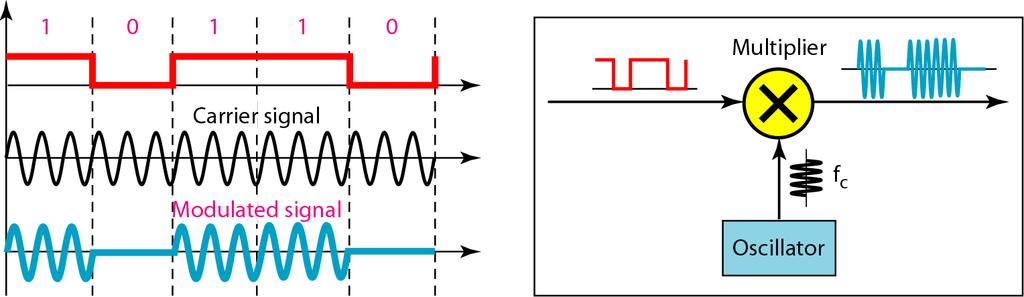
59 Unit-5 Error ControlCoding Memoryless modulation techniques Modulation is defined as the process by which some characteristics of a carrier is varied in accordance with a modulating wave. In digital communications, the modulating wave consists of binary data or an M-ary encoded version of it and the carrier is sinusoidal wave. Different Shift keying methods that are used in digital modulation techniques are Amplitude shift keying [ASK] Frequency shift keying [FSK] Phase shift keying [PSK] Fig shows different modulations 59
60 Hierarchy of digital modulation technique Digital Modulation Technique Coherent Non - Coherent Binary (m) = 2 M - ary Hybrid Binary (m) = 2 M - ary * ASK M-ary ASK M-ary APK * FSK M-ary FSK M-ary QAM * PSK M-ary PSK (QPSK) * ASK M-ary ASK * FSK M-ary FSK * DPSK M-ary DPSK 60
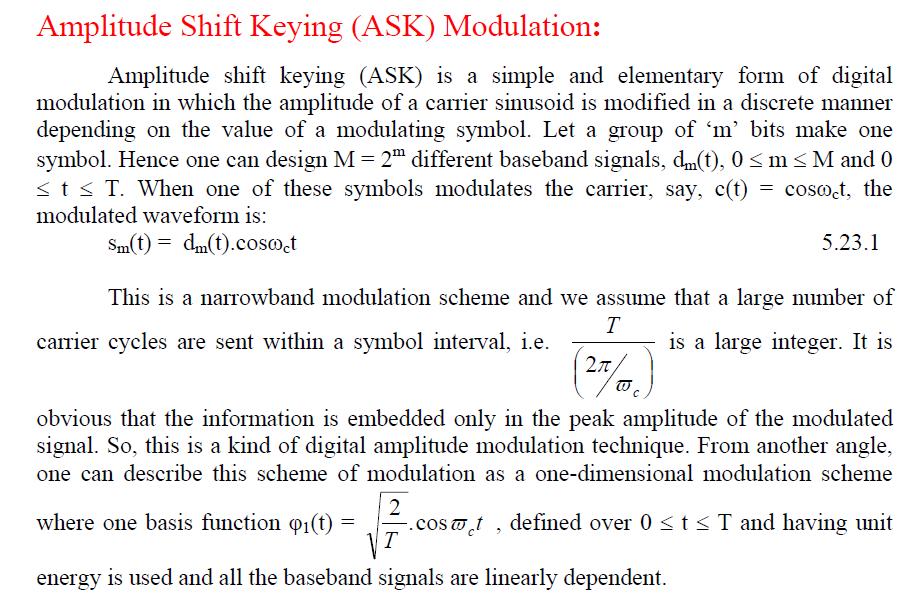
61 Implementation of binary ASK: 61
 0 E b 2 Message Point 1 Signal Space representation of BASK signal In transmitter the binary data sequence is given to an on-off encoder.")
62 BINARY AMPLITUDE SHIFT KEYING, BANDWIDTH: d 0-related to the condition of the line B = (1+d) x S = (1+d) x N x 1/r The BASK system has one dimensional signal space with two messages (N=1, M=2) Region E 2 Region E 1 Message Point 2 E b ᶲ(t) 0 E b 2 Message Point 1 Signal Space representation of BASK signal In transmitter the binary data sequence is given to an on-off encoder. Which gives an output E b volts for symbol 1 and 0 volt for symbol 0. The resulting binary wave [in unipolar form] and sinusoidal carrier are applied to a product modulator. The desired BASK wave is obtained at the modulator output. 62

63 In demodulator, the received noisy BASK signal x(t) is apply to correlator with coherent reference signal. The correlator output x is compared with threshold λ. If x > λ the receiver decides in favour of symbol 1. If x < λ the receiver decides in favour of symbol 0. Generation and Detection:- 63
64 FSK transmitter fig b FSK receiver A binary FSK Transmitter is as shown,the incoming binary data sequence is applied to on-off level encoder. The output of encoder is E b volts for symbol 1 and 0 volts for symbol 0. When we have symbol 1 the upper channel is switched on with oscillator frequency f 1, for symbol 0, because of inverter the lower channel is switched on with oscillator frequency f 2. These two frequencies are combined using an adder circuit and then transmitted. required BFSK signal. The transmitted signal is nothing but The detector consists of two correlators. The incoming noisy BFSK signal x(t) is common to both correlator. The Coherent reference signal ᶲ 1 (t) & ᶲ 2 (t) are supplied to upper and lower correlators respectively. The correlator outputs are then subtracted one from the other and resulting a random vector l (l=x 1 - x 2 ). The output l is compared with threshold of zero volts. If l > 0, the receiver decides in favour of symbol 1. l < 0, the receiver decides in favour of symbol 0. FSK Bandwidth: 64

65 Limiting factor: Physical capabilities of the carrier Not susceptible to noise as much as ASK Applications On voice-grade lines, used up to 1200bps Used for high-frequency (3 to 30 MHz) radio transmission used at higher frequencies on LANs that use coaxial cable. Therefore Binary FSK system has 2 dimensional signal space with two messages S 1 (t) and S 2 (t), [N=2, m=2] they are represented, Fig. Signal Space diagram of Coherent binary FSK system. 65
66 PHASE SHIFT KEYING(PSK): Binary Data Sequence Non Return to Zero Level Encoder Product Modulator Binary PSK Signal 1 (t) 2 Cos2 f c t T b Fig(a) Block diagram of BPSK transmitter x(t) T b dt 0 x 1 Decision Device Choose 1 if x 1 >0 Choose 0 if x 1 <0 1 (t) Correlator Threshold λ = 0 Fig (b) Coherent binary PSK receiver In a Coherent binary PSK system the pair of signals S 1 (t) and S 2 (t) are used to represent binary symbol 1 and 0 respectively. To generate a binary PSK signal we have to represent the input binary sequence in polar form with symbol 1 and 0 represented by constant amplitude levels To detect the original binary sequence of 1 s and 0 s we apply the noisy PSK signal x(t) to a Correlator, which is also supplied with a locally generated coherent reference signal The correlator output x 1 is compared with a threshold of zero volt. If x 1 > 0, the receiver decides in favour of symbol 1. If x 1 < 0, the receiver decides in favour of symbol 0. 66
67 The signal space representation is as shown in fig (N=1 & M=2) Region R 2 Region R 1 - E b E b Message Point 2 S 2 (t) 0 Decision Boundary Message Point 1 S 1 (t) Fig. Signal Space Representation of BPSK QUADRATURE PHASE SHIFT KEYING(QPSK) In a sense, QPSK is an expanded version from binary PSK where in a symbol consists of two bits and two orthonormal basis functions are used. A group of two bits is often called a dibit. So, four dibits are possible. Each symbol carries same energy. Let, E: Energy per Symbol and T: SymbolDuration = 2.* Tb, where Tb: duration of 1 bit. Fig. (a) QPSK Transmitter 67
68 Fig. (b) QPSK Receiver Fig. QPSK Waveform the phase. In QPSK system the information carried by the transmitted signal is contained in 68
 are each compared with a threshold value of zero.")
69 QPSK Receiver:- The QPSK receiver consists of a pair of correlators with a common input and supplied with a locally generated pair of coherent reference signals ᶲ 1 (t) & ᶲ 2 (t)as shown in fig(b).the correlator outputs x 1 and x 2 produced in response to the received signal x(t) are each compared with a threshold value of zero. The in-phase channel output : If x 1 > 0 a decision is made in favour of symbol 1 x 1 < 0 a decision is made in favour of symbol 0 Similarly quadrature channel output: If x 2 >0 a decision is made in favour of symbol 1 and x 2 <0 a decision is made in favour of symbol 0 Finally these two binary sequences at the in phase and quadrature channel outputs are combined in a multiplexer (Parallel to Serial) to reproduce the original binary sequence. Probability of error:- A QPSK system is in fact equivalent to two coherent binary PSK systems working in parallel and using carriers that are in-phase and quadrature. The in-phase channel output x 1 and the Q-channel output x 2 may be viewed as the individual outputs of the two coherent binary PSK systems. Thus the two binary PSK systems may be characterized as follows. - The signal energy per bit E 2 69
UNIT-1. Basic signal processing operations in digital communication
 UNIT-1 Lecture-1 Basic signal processing operations in digital communication The three basic elements of every communication systems are Transmitter, Receiver and Channel. The Overall purpose of this system
Chapter-1: Introduction
 Chapter-1: Introduction The purpose of a Communication System is to transport an information bearing signal from a source to a user destination via a communication channel. MODEL OF A COMMUNICATION SYSTEM
CHAPTER 3 Syllabus (2006 scheme syllabus) Differential pulse code modulation DPCM transmitter
 Differential pulse code modulation DPCM transmitter") CHAPTER 3 Syllabus 1) DPCM 2) DM 3) Base band shaping for data tranmission 4) Discrete PAM signals 5) Power spectra of discrete PAM signal. 6) Applications (2006 scheme syllabus) Differential pulse code
CHAPTER 3 Syllabus 1) DPCM 2) DM 3) Base band shaping for data tranmission 4) Discrete PAM signals 5) Power spectra of discrete PAM signal. 6) Applications (2006 scheme syllabus) Differential pulse code
Time division multiplexing The block diagram for TDM is illustrated as shown in the figure
 CHAPTER 2 Syllabus: 1) Pulse amplitude modulation 2) TDM 3) Wave form coding techniques 4) PCM 5) Quantization noise and SNR 6) Robust quantization Pulse amplitude modulation In pulse amplitude modulation,
EEE 309 Communication Theory
 EEE 309 Communication Theory Semester: January 2016 Dr. Md. Farhad Hossain Associate Professor Department of EEE, BUET Email: mfarhadhossain@eee.buet.ac.bd Office: ECE 331, ECE Building Part 05 Pulse Code
Chapter-2 SAMPLING PROCESS
 Chapter-2 SAMPLING PROCESS SAMPLING: A message signal may originate from a digital or analog source. If the message signal is analog in nature, then it has to be converted into digital form before it can
QUESTION BANK EC 1351 DIGITAL COMMUNICATION YEAR / SEM : III / VI UNIT I- PULSE MODULATION PART-A (2 Marks) 1. What is the purpose of sample and hold
 1. What is the purpose of sample and hold") QUESTION BANK EC 1351 DIGITAL COMMUNICATION YEAR / SEM : III / VI UNIT I- PULSE MODULATION PART-A (2 Marks) 1. What is the purpose of sample and hold circuit 2. What is the difference between natural sampling
QUESTION BANK EC 1351 DIGITAL COMMUNICATION YEAR / SEM : III / VI UNIT I- PULSE MODULATION PART-A (2 Marks) 1. What is the purpose of sample and hold circuit 2. What is the difference between natural sampling
EC 6501 DIGITAL COMMUNICATION UNIT - II PART A
 EC 6501 DIGITAL COMMUNICATION 1.What is the need of prediction filtering? UNIT - II PART A [N/D-16] Prediction filtering is used mostly in audio signal processing and speech processing for representing
Chapter-3 Waveform Coding Techniques
 Chapter-3 Waveform Coding Techniques PCM [Pulse Code Modulation] PCM is an important method of analog to-digital conversion. In this modulation the analog signal is converted into an electrical waveform
EEE 309 Communication Theory
 EEE 309 Communication Theory Semester: January 2017 Dr. Md. Farhad Hossain Associate Professor Department of EEE, BUET Email: mfarhadhossain@eee.buet.ac.bd Office: ECE 331, ECE Building Types of Modulation
EC 2301 Digital communication Question bank
 EC 2301 Digital communication Question bank UNIT I Digital communication system 2 marks 1.Draw block diagram of digital communication system. Information source and input transducer formatter Source encoder
PULSE CODE MODULATION (PCM)
") PULSE CODE MODULATION (PCM) 1. PCM quantization Techniques 2. PCM Transmission Bandwidth 3. PCM Coding Techniques 4. PCM Integrated Circuits 5. Advantages of PCM 6. Delta Modulation 7. Adaptive Delta Modulation
PULSE CODE MODULATION (PCM) 1. PCM quantization Techniques 2. PCM Transmission Bandwidth 3. PCM Coding Techniques 4. PCM Integrated Circuits 5. Advantages of PCM 6. Delta Modulation 7. Adaptive Delta Modulation
QUESTION BANK. SUBJECT CODE / Name: EC2301 DIGITAL COMMUNICATION UNIT 2
 QUESTION BANK DEPARTMENT: ECE SEMESTER: V SUBJECT CODE / Name: EC2301 DIGITAL COMMUNICATION UNIT 2 BASEBAND FORMATTING TECHNIQUES 1. Why prefilterring done before sampling [AUC NOV/DEC 2010] The signal
Department of Electronics and Communication Engineering 1
 UNIT I SAMPLING AND QUANTIZATION Pulse Modulation 1. Explain in detail the generation of PWM and PPM signals (16) (M/J 2011) 2. Explain in detail the concept of PWM and PAM (16) (N/D 2012) 3. What is the
DHANALAKSHMI COLLEGE OF ENGINEERING ELECTRONICS AND COMMUNICATION ENGINEERING EC DIGITAL COMMUNICATION DCE
 DHANALAKSHMI COLLEGE OF ENGINEERING ELECTRONICS AND COMMUNICATION ENGINEERING EC 6501 - S.No CONTENTS PAGE NO UNIT I SAMPLING & QUANTIZATION 1.1 Sampling theorem for Low pass signals 01 1.2 Aliasing and
Communications I (ELCN 306)
") Communications I (ELCN 306) c Samy S. Soliman Electronics and Electrical Communications Engineering Department Cairo University, Egypt Email: samy.soliman@cu.edu.eg Website: http://scholar.cu.edu.eg/samysoliman
Communications I (ELCN 306) c Samy S. Soliman Electronics and Electrical Communications Engineering Department Cairo University, Egypt Email: samy.soliman@cu.edu.eg Website: http://scholar.cu.edu.eg/samysoliman
MAHALAKSHMI ENGINEERING COLLEGE TIRUCHIRAPALLI
 MAHALAKSHMI ENGINEERING COLLEGE TIRUCHIRAPALLI 621213 QUESTION BANK DEPARTMENT: ECE SEMESTER: V SUBJECT CODE / Name: EC2301 DIGITAL COMMUNICATION UNIT-I DIGITAL COMMUNICATION SYSTEMS PART -A (2 Marks)
Communications and Signals Processing
 Communications and Signals Processing Dr. Ahmed Masri Department of Communications An Najah National University 2012/2013 1 Dr. Ahmed Masri Chapter 5 - Outlines 5.4 Completing the Transition from Analog
CODING TECHNIQUES FOR ANALOG SOURCES
 CODING TECHNIQUES FOR ANALOG SOURCES Prof.Pratik Tawde Lecturer, Electronics and Telecommunication Department, Vidyalankar Polytechnic, Wadala (India) ABSTRACT Image Compression is a process of removing
LATHA MATHAVAN ENGINEERING COLLEGE Alagarkovil, Madurai
 UNIT I - SAMPLING & QUANTIZATION PART A 1. What is aliasing? (EC6501 June 2016) 2. What is Companding? Sketch the input-output characteristics of a compressor and an expander. (EC6501 June 2016) 3. An
Lecture 3 Concepts for the Data Communications and Computer Interconnection
 Lecture 3 Concepts for the Data Communications and Computer Interconnection Aim: overview of existing methods and techniques Terms used: -Data entities conveying meaning (of information) -Signals data
Downloaded from 1
 VII SEMESTER FINAL EXAMINATION-2004 Attempt ALL questions. Q. [1] How does Digital communication System differ from Analog systems? Draw functional block diagram of DCS and explain the significance of
Fundamentals of Digital Communication
 Fundamentals of Digital Communication Network Infrastructures A.A. 2017/18 Digital communication system Analog Digital Input Signal Analog/ Digital Low Pass Filter Sampler Quantizer Source Encoder Channel
EC6501 Digital Communication
 EC6501 Digital Communication UNIT -1 DIGITAL COMMUNICATION SYSTEMS Digital Communication system 1) Write the advantages and disadvantages of digital communication. [A/M 11] The advantages of digital communication
Digital Communication (650533) CH 3 Pulse Modulation
 CH 3 Pulse Modulation") Philadelphia University/Faculty of Engineering Communication and Electronics Engineering Digital Communication (650533) CH 3 Pulse Modulation Instructor: Eng. Nada Khatib Website: http://www.philadelphia.edu.jo/academics/nkhatib/
Philadelphia University/Faculty of Engineering Communication and Electronics Engineering Digital Communication (650533) CH 3 Pulse Modulation Instructor: Eng. Nada Khatib Website: http://www.philadelphia.edu.jo/academics/nkhatib/
QUESTION BANK SUBJECT: DIGITAL COMMUNICATION (15EC61)
") QUESTION BANK SUBJECT: DIGITAL COMMUNICATION (15EC61) Module 1 1. Explain Digital communication system with a neat block diagram. 2. What are the differences between digital and analog communication systems?
QUESTION BANK SUBJECT: DIGITAL COMMUNICATION (15EC61) Module 1 1. Explain Digital communication system with a neat block diagram. 2. What are the differences between digital and analog communication systems?
6. FUNDAMENTALS OF CHANNEL CODER
 82 6. FUNDAMENTALS OF CHANNEL CODER 6.1 INTRODUCTION The digital information can be transmitted over the channel using different signaling schemes. The type of the signal scheme chosen mainly depends on
TE 302 DISCRETE SIGNALS AND SYSTEMS. Chapter 1: INTRODUCTION
 TE 302 DISCRETE SIGNALS AND SYSTEMS Study on the behavior and processing of information bearing functions as they are currently used in human communication and the systems involved. Chapter 1: INTRODUCTION
Syllabus. osmania university UNIT - I UNIT - II UNIT - III CHAPTER - 1 : INTRODUCTION TO DIGITAL COMMUNICATION CHAPTER - 3 : INFORMATION THEORY
 i Syllabus osmania university UNIT - I CHAPTER - 1 : INTRODUCTION TO Elements of Digital Communication System, Comparison of Digital and Analog Communication Systems. CHAPTER - 2 : DIGITAL TRANSMISSION
KINGS COLLEGE OF ENGINEERING DEPARTMENT OF ELECTRONICS AND COMMUNICATION ENGINEERING QUESTION BANK. Subject Name: Digital Communication Techniques
 KINGS COLLEGE OF ENGINEERING DEPARTMENT OF ELECTRONICS AND COMMUNICATION ENGINEERING QUESTION BANK Subject Code: EC1351 Year/Sem: III/IV Subject Name: Digital Communication Techniques UNIT I PULSE MODULATION
EXPERIMENT WISE VIVA QUESTIONS
 EXPERIMENT WISE VIVA QUESTIONS Pulse Code Modulation: 1. Draw the block diagram of basic digital communication system. How it is different from analog communication system. 2. What are the advantages of
UNIT I Source Coding Systems
 SIDDHARTH GROUP OF INSTITUTIONS: PUTTUR Siddharth Nagar, Narayanavanam Road 517583 QUESTION BANK (DESCRIPTIVE) Subject with Code: DC (16EC421) Year & Sem: III-B. Tech & II-Sem Course & Branch: B. Tech
UNIT TEST I Digital Communication
 Time: 1 Hour Class: T.E. I & II Max. Marks: 30 Q.1) (a) A compact disc (CD) records audio signals digitally by using PCM. Assume the audio signal B.W. to be 15 khz. (I) Find Nyquist rate. (II) If the Nyquist
Comm 502: Communication Theory. Lecture 4. Line Coding M-ary PCM-Delta Modulation
 Comm 502: Communication Theory Lecture 4 Line Coding M-ary PCM-Delta Modulation PCM Decoder PCM Waveform Types (Line Coding) Representation of binary sequence into the electrical signals that enter the
QUESTION BANK (VI SEM ECE) (DIGITAL COMMUNICATION)
 (DIGITAL COMMUNICATION)") QUESTION BANK (VI SEM ECE) (DIGITAL COMMUNICATION) UNIT-I: PCM & Delta modulation system Q.1 Explain the difference between cross talk & intersymbol interference. Q.2 What is Quantization error? How does
QUESTION BANK (VI SEM ECE) (DIGITAL COMMUNICATION) UNIT-I: PCM & Delta modulation system Q.1 Explain the difference between cross talk & intersymbol interference. Q.2 What is Quantization error? How does
KINGS DEPARTMENT OF ELECTRONICS AND COMMUNICATION ENGINEERING DIGITAL COMMUNICATION TECHNIQUES YEAR/SEM: III / VI BRANCH : ECE PULSE MODULATION
 KINGS COLLEGE OF ENGINEERING DEPARTMENT OF ELECTRONICS AND COMMUNICATION ENGINEERING SUB.NAME : EC1351 DIGITAL COMMUNICATION TECHNIQUES BRANCH : ECE YEAR/SEM: III / VI UNIT I PULSE MODULATION PART A (2
Chapter 2: Fundamentals of Data and Signals
 Chapter 2: Fundamentals of Data and Signals TRUE/FALSE 1. The terms data and signal mean the same thing. F PTS: 1 REF: 30 2. By convention, the minimum and maximum values of analog data and signals are
DIGITAL COMMINICATIONS
 Code No: R346 R Set No: III B.Tech. I Semester Regular and Supplementary Examinations, December - 23 DIGITAL COMMINICATIONS (Electronics and Communication Engineering) Time: 3 Hours Max Marks: 75 Answer
10 Speech and Audio Signals
 0 Speech and Audio Signals Introduction Speech and audio signals are normally converted into PCM, which can be stored or transmitted as a PCM code, or compressed to reduce the number of bits used to code
CHAPTER 4. PULSE MODULATION Part 2
 CHAPTER 4 PULSE MODULATION Part 2 Pulse Modulation Analog pulse modulation: Sampling, i.e., information is transmitted only at discrete time instants. e.g. PAM, PPM and PDM Digital pulse modulation: Sampling
 Sixth Semester B.E. Degree Examination, May/June 2010 Digital Communication Note: Answer any FIVEfull questions, selecting at least TWO questionsfrom each part. PART-A a. With a block diagram, explain
Physical Layer: Modulation, FEC. Wireless Networks: Guevara Noubir. S2001, COM3525 Wireless Networks Lecture 3, 1
 Wireless Networks: Physical Layer: Modulation, FEC Guevara Noubir Noubir@ccsneuedu S, COM355 Wireless Networks Lecture 3, Lecture focus Modulation techniques Bit Error Rate Reducing the BER Forward Error
Pulse Code Modulation
 Pulse Code Modulation Modulation is the process of varying one or more parameters of a carrier signal in accordance with the instantaneous values of the message signal. The message signal is the signal
SEN366 Computer Networks
 SEN366 Computer Networks Prof. Dr. Hasan Hüseyin BALIK (5 th Week) 5. Signal Encoding Techniques 5.Outline An overview of the basic methods of encoding digital data into a digital signal An overview of
2. By convention, the minimum and maximum values of analog data and signals are presented as voltages.
 Chapter 2: Fundamentals of Data and Signals Data Communications and Computer Networks A Business Users Approach 8th Edition White TEST BANK Full clear download (no formatting errors) at: https://testbankreal.com/download/data-communications-computer-networksbusiness-users-approach-8th-edition-white-test-bank/
Class 4 ((Communication and Computer Networks))
)") Class 4 ((Communication and Computer Networks)) Lesson 5... SIGNAL ENCODING TECHNIQUES Abstract Both analog and digital information can be encoded as either analog or digital signals. The particular encoding
Class 4 ((Communication and Computer Networks)) Lesson 5... SIGNAL ENCODING TECHNIQUES Abstract Both analog and digital information can be encoded as either analog or digital signals. The particular encoding
Pulse Code Modulation
 Pulse Code Modulation EE 44 Spring Semester Lecture 9 Analog signal Pulse Amplitude Modulation Pulse Width Modulation Pulse Position Modulation Pulse Code Modulation (3-bit coding) 1 Advantages of Digital
AMSEC/ECE
 EC6501 -DIGITAL COMMUNICATION UNIT-I SAMPLING & QUANTIZATION 1. Define Dirac comb or ideal sampling function. What is its Fourier Transform? Dirac comb is nothing but a periodic impulse train in which
Convolutional Coding Using Booth Algorithm For Application in Wireless Communication
 Available online at www.interscience.in Convolutional Coding Using Booth Algorithm For Application in Wireless Communication Sishir Kalita, Parismita Gogoi & Kandarpa Kumar Sarma Department of Electronics
SIGNALS AND SYSTEMS LABORATORY 13: Digital Communication
 SIGNALS AND SYSTEMS LABORATORY 13: Digital Communication INTRODUCTION Digital Communication refers to the transmission of binary, or digital, information over analog channels. In this laboratory you will
Digital Communication - Analog to Digital
 Unit 26. Digital Communication Digital Communication - Analog to Digital The communication that occurs in our day-to-day life is in the form of signals. These signals, such as sound signals, generally,
Theory of Telecommunications Networks
 Theory of Telecommunications Networks Anton Čižmár Ján Papaj Department of electronics and multimedia telecommunications CONTENTS Preface... 5 1 Introduction... 6 1.1 Mathematical models for communication
Digital data (a sequence of binary bits) can be transmitted by various pule waveforms.
 can be transmitted by various pule waveforms.") Chapter 2 Line Coding Digital data (a sequence of binary bits) can be transmitted by various pule waveforms. Sometimes these pulse waveforms have been called line codes. 2.1 Signalling Format Figure 2.1
Chapter 2 Line Coding Digital data (a sequence of binary bits) can be transmitted by various pule waveforms. Sometimes these pulse waveforms have been called line codes. 2.1 Signalling Format Figure 2.1
Physical Layer: Outline
 18-345: Introduction to Telecommunication Networks Lectures 3: Physical Layer Peter Steenkiste Spring 2015 www.cs.cmu.edu/~prs/nets-ece Physical Layer: Outline Digital networking Modulation Characterization
QUESTION BANK. Staff In-Charge: M.MAHARAJA, AP / ECE
 FATIMA MICHAEL COLLEGE OF ENGINEERING & TECHNOLOGY Senkottai Village, Madurai Sivagangai Main Road, Madurai -625 020 An ISO 9001:2008 Certified Institution QUESTION BANK Sub. Code : EC 2301 Class : III
Chapter 2: Signal Representation
 Chapter 2: Signal Representation Aveek Dutta Assistant Professor Department of Electrical and Computer Engineering University at Albany Spring 2018 Images and equations adopted from: Digital Communications
Lecture Fundamentals of Data and signals
 IT-5301-3 Data Communications and Computer Networks Lecture 05-07 Fundamentals of Data and signals Lecture 05 - Roadmap Analog and Digital Data Analog Signals, Digital Signals Periodic and Aperiodic Signals
 UNIT III -- DATA AND PULSE COMMUNICATION PART-A 1. State the sampling theorem for band-limited signals of finite energy. If a finite energy signal g(t) contains no frequency higher than W Hz, it is completely
Department of Electronics & Telecommunication Engg. LAB MANUAL. B.Tech V Semester [ ] (Branch: ETE)
![Department of Electronics & Telecommunication Engg. LAB MANUAL. B.Tech V Semester [ ] (Branch: ETE)](/thumbs/86/93078052.jpg "Department of Electronics & Telecommunication Engg. LAB MANUAL. B.Tech V Semester [ ] (Branch: ETE)") Department of Electronics & Telecommunication Engg. LAB MANUAL SUBJECT:-DIGITAL COMMUNICATION SYSTEM [BTEC-501] B.Tech V Semester [2013-14] (Branch: ETE) KCT COLLEGE OF ENGG & TECH., FATEHGARH PUNJAB TECHNICAL
Department of Electronics & Telecommunication Engg. LAB MANUAL SUBJECT:-DIGITAL COMMUNICATION SYSTEM [BTEC-501] B.Tech V Semester [2013-14] (Branch: ETE) KCT COLLEGE OF ENGG & TECH., FATEHGARH PUNJAB TECHNICAL
Outline. Communications Engineering 1
 Outline Introduction Signal, random variable, random process and spectra Analog modulation Analog to digital conversion Digital transmission through baseband channels Signal space representation Optimal
Computer Networks - Xarxes de Computadors
 Computer Networks - Xarxes de Computadors Outline Course Syllabus Unit 1: Introduction Unit 2. IP Networks Unit 3. Point to Point Protocols -TCP Unit 4. Local Area Networks, LANs 1 Outline Introduction
Handout 11: Digital Baseband Transmission
 ENGG 23-B: Principles of Communication Systems 27 8 First Term Handout : Digital Baseband Transmission Instructor: Wing-Kin Ma November 7, 27 Suggested Reading: Chapter 8 of Simon Haykin and Michael Moher,
Voice Transmission --Basic Concepts--
 Voice Transmission --Basic Concepts-- Voice---is analog in character and moves in the form of waves. 3-important wave-characteristics: Amplitude Frequency Phase Telephone Handset (has 2-parts) 2 1. Transmitter
(Refer Slide Time: 3:11)
") Digital Communication. Professor Surendra Prasad. Department of Electrical Engineering. Indian Institute of Technology, Delhi. Lecture-2. Digital Representation of Analog Signals: Delta Modulation. Professor:
Digital Communication. Professor Surendra Prasad. Department of Electrical Engineering. Indian Institute of Technology, Delhi. Lecture-2. Digital Representation of Analog Signals: Delta Modulation. Professor:
Digital Communication Prof. Bikash Kumar Dey Department of Electrical Engineering Indian Institute of Technology, Bombay
 Digital Communication Prof. Bikash Kumar Dey Department of Electrical Engineering Indian Institute of Technology, Bombay Lecture - 03 Quantization, PCM and Delta Modulation Hello everyone, today we will
UNIT I AMPLITUDE MODULATION
 UNIT I AMPLITUDE MODULATION Prepared by: S.NANDHINI, Assistant Professor, Dept. of ECE, Sri Venkateswara College of Engineering, Sriperumbudur, Tamilnadu. CONTENTS Introduction to communication systems
UNIT I ELEMENTS OF DIGITAL COMMUNICATION SYSTEMS
 UNIT I ELEMENTS OF DIGITAL COMMUNICATION SYSTEMS The purpose of a Communication System is to transport an information bearing signal from a source to a user destination via a communication channel. MODEL
DEPARTMENT OF CSE QUESTION BANK
 DEPARTMENT OF CSE QUESTION BANK SUBJECT CODE: CS6304 SUBJECT NAME: ANALOG AND DIGITAL COMMUNICATION Part-A UNIT-I ANALOG COMMUNICATION 1.Define modulation? Modulation is a process by which some characteristics
Introduction to Discrete-Time Control Systems
 Chapter 1 Introduction to Discrete-Time Control Systems 1-1 INTRODUCTION The use of digital or discrete technology to maintain conditions in operating systems as close as possible to desired values despite
Outline / Wireless Networks and Applications Lecture 3: Physical Layer Signals, Modulation, Multiplexing. Cartoon View 1 A Wave of Energy
 Outline 18-452/18-750 Wireless Networks and Applications Lecture 3: Physical Layer Signals, Modulation, Multiplexing Peter Steenkiste Carnegie Mellon University Spring Semester 2017 http://www.cs.cmu.edu/~prs/wirelesss17/
Principles of Baseband Digital Data Transmission
 Principles of Baseband Digital Data Transmission Prof. Wangrok Oh Dept. of Information Communications Eng. Chungnam National University Prof. Wangrok Oh(CNU) / 3 Overview Baseband Digital Data Transmission
7.1 Introduction 7.2 Why Digitize Analog Sources? 7.3 The Sampling Process 7.4 Pulse-Amplitude Modulation Time-Division i i Modulation 7.
 Chapter 7 Digital Representation of Analog Signals Wireless Information Transmission System Lab. Institute of Communications Engineering g National Sun Yat-sen University Contents 7.1 Introduction 7.2
Part A: Question & Answers UNIT I AMPLITUDE MODULATION
 PANDIAN SARASWATHI YADAV ENGINEERING COLLEGE DEPARTMENT OF ELECTRONICS & COMMUNICATON ENGG. Branch: ECE EC6402 COMMUNICATION THEORY Semester: IV Part A: Question & Answers UNIT I AMPLITUDE MODULATION 1.
EEE482F: Problem Set 1
 EEE482F: Problem Set 1 1. A digital source emits 1.0 and 0.0V levels with a probability of 0.2 each, and +3.0 and +4.0V levels with a probability of 0.3 each. Evaluate the average information of the source.
TCET3202 Analog and digital Communications II
 NEW YORK CITY COLLEGE OF TECHNOLOGY The City University of New York DEPARTMENT: SUBJECT CODE AND TITLE: COURSE DESCRIPTION: REQUIRED COURSE Electrical and Telecommunications Engineering Technology TCET3202
Department of Electronics & Communication Engineering LAB MANUAL SUBJECT: DIGITAL COMMUNICATION LABORATORY [ECE324] (Branch: ECE)
![Department of Electronics & Communication Engineering LAB MANUAL SUBJECT: DIGITAL COMMUNICATION LABORATORY [ECE324] (Branch: ECE)](/thumbs/96/127341232.jpg "Department of Electronics & Communication Engineering LAB MANUAL SUBJECT: DIGITAL COMMUNICATION LABORATORY [ECE324] (Branch: ECE)") Department of Electronics & Communication Engineering LAB MANUAL SUBJECT: DIGITAL COMMUNICATION LABORATORY [ECE324] B.Tech Year 3 rd, Semester - 5 th (Branch: ECE) Version: 01 st August 2018 The LNM Institute
Department of Electronics & Communication Engineering LAB MANUAL SUBJECT: DIGITAL COMMUNICATION LABORATORY [ECE324] B.Tech Year 3 rd, Semester - 5 th (Branch: ECE) Version: 01 st August 2018 The LNM Institute
Chapter 3 Pulse Modulation
 Chapter 3 Pulse Modulation Outline Sampling Process: Sampling Theory, Anti-Aliasing Pulse Modulation Analog Pulse Modulation: PAM, PDM, PWM, PPM Digital Pulse Modulation: PCM, DM, DPCM Quantization Process:
ECE 556 BASICS OF DIGITAL SPEECH PROCESSING. Assıst.Prof.Dr. Selma ÖZAYDIN Spring Term-2017 Lecture 2
 ECE 556 BASICS OF DIGITAL SPEECH PROCESSING Assıst.Prof.Dr. Selma ÖZAYDIN Spring Term-2017 Lecture 2 Analog Sound to Digital Sound Characteristics of Sound Amplitude Wavelength (w) Frequency ( ) Timbre
Signal Encoding Techniques
 2 Techniques ITS323: to Data Communications CSS331: Fundamentals of Data Communications Sirindhorn International Institute of Technology Thammasat University Prepared by Steven Gordon on 3 August 2015
Digital Transmission (Line Coding) EE4367 Telecom. Switching & Transmission. Pulse Transmission
 EE4367 Telecom. Switching & Transmission. Pulse Transmission") Digital Transmission (Line Coding) Pulse Transmission Source Multiplexer Line Coder Line Coding: Output of the multiplexer (TDM) is coded into electrical pulses or waveforms for the purpose of transmission
Digital Transmission (Line Coding) Pulse Transmission Source Multiplexer Line Coder Line Coding: Output of the multiplexer (TDM) is coded into electrical pulses or waveforms for the purpose of transmission
DEPARTMENT OF INFORMATION TECHNOLOGY QUESTION BANK. Subject Name: Information Coding Techniques UNIT I INFORMATION ENTROPY FUNDAMENTALS
 DEPARTMENT OF INFORMATION TECHNOLOGY QUESTION BANK Subject Name: Year /Sem: II / IV UNIT I INFORMATION ENTROPY FUNDAMENTALS PART A (2 MARKS) 1. What is uncertainty? 2. What is prefix coding? 3. State the
Problem Sheet 1 Probability, random processes, and noise
 Problem Sheet 1 Probability, random processes, and noise 1. If F X (x) is the distribution function of a random variable X and x 1 x 2, show that F X (x 1 ) F X (x 2 ). 2. Use the definition of the cumulative
2. TELECOMMUNICATIONS BASICS
 2. TELECOMMUNICATIONS BASICS The purpose of any telecommunications system is to transfer information from the sender to the receiver by a means of a communication channel. The information is carried by
SKP Engineering College
 SKP Engineering College Tiruvannamalai 606611 A Course Material on Digital Communication By Dr.P.Sivakumar Professor Electronics and Communication Engineering Department Electronics and Communication Engineering
Introduction to Telecommunications and Computer Engineering Unit 3: Communications Systems & Signals
 Introduction to Telecommunications and Computer Engineering Unit 3: Communications Systems & Signals Syedur Rahman Lecturer, CSE Department North South University syedur.rahman@wolfson.oxon.org Acknowledgements
Speech, music, images, and video are examples of analog signals. Each of these signals is characterized by its bandwidth, dynamic range, and the
 Speech, music, images, and video are examples of analog signals. Each of these signals is characterized by its bandwidth, dynamic range, and the nature of the signal. For instance, in the case of audio
3.6 Intersymbol interference. 1 Your site here
 3.6 Intersymbol intererence 1 3.6 Intersymbol intererence what is intersymbol intererence and what cause ISI 1. The absolute bandwidth o rectangular multilevel pulses is ininite. The channels bandwidth
Chapter 1 INTRODUCTION TO SOURCE CODING AND CHANNEL CODING. Whether a source is analog or digital, a digital communication
 1 Chapter 1 INTRODUCTION TO SOURCE CODING AND CHANNEL CODING 1.1 SOURCE CODING Whether a source is analog or digital, a digital communication system is designed to transmit information in digital form.
Digital signal is denoted by discreet signal, which represents digital data.there are three types of line coding schemes available:
 Digital-to-Digital Conversion This section explains how to convert digital data into digital signals. It can be done in two ways, line coding and block coding. For all communications, line coding is necessary
Jitter in Digital Communication Systems, Part 1
 Application Note: HFAN-4.0.3 Rev.; 04/08 Jitter in Digital Communication Systems, Part [Some parts of this application note first appeared in Electronic Engineering Times on August 27, 200, Issue 8.] AVAILABLE
Year : TYEJ Sub: Digital Communication (17535) Assignment No. 1. Introduction of Digital Communication. Question Exam Marks
 Assignment No. 1. Introduction of Digital Communication. Question Exam Marks") Assignment 1 Introduction of Digital Communication Sr. Question Exam Marks 1 Draw the block diagram of the basic digital communication system. State the function of each block in detail. W 2015 6 2 State
Assignment 1 Introduction of Digital Communication Sr. Question Exam Marks 1 Draw the block diagram of the basic digital communication system. State the function of each block in detail. W 2015 6 2 State
Data Communication. Chapter 3 Data Transmission
 Data Communication Chapter 3 Data Transmission ١ Terminology (1) Transmitter Receiver Medium Guided medium e.g. twisted pair, coaxial cable, optical fiber Unguided medium e.g. air, water, vacuum ٢ Terminology
Level 6 Graduate Diploma in Engineering Communication systems
 9210-118 Level 6 Graduate Diploma in Engineering Communication systems Sample Paper You should have the following for this examination one answer book non-programmable calculator pen, pencil, ruler, drawing
CSCD 433 Network Programming Fall Lecture 5 Physical Layer Continued
 CSCD 433 Network Programming Fall 2016 Lecture 5 Physical Layer Continued 1 Topics Definitions Analog Transmission of Digital Data Digital Transmission of Analog Data Multiplexing 2 Different Types of
Chapter 2 Direct-Sequence Systems
 Chapter 2 Direct-Sequence Systems A spread-spectrum signal is one with an extra modulation that expands the signal bandwidth greatly beyond what is required by the underlying coded-data modulation. Spread-spectrum
Communication Channels
 Communication Channels wires (PCB trace or conductor on IC) optical fiber (attenuation 4dB/km) broadcast TV (50 kw transmit) voice telephone line (under -9 dbm or 110 µw) walkie-talkie: 500 mw, 467 MHz
Review of Lecture 2. Data and Signals - Theoretical Concepts. Review of Lecture 2. Review of Lecture 2. Review of Lecture 2. Review of Lecture 2
 Data and Signals - Theoretical Concepts! What are the major functions of the network access layer? Reference: Chapter 3 - Stallings Chapter 3 - Forouzan Study Guide 3 1 2! What are the major functions
Data Encoding g(p (part 2)
") Data Encoding g(p (part 2) CSE 3213 Instructor: U.T. Nguyen 10/11/2007 12:44 PM 1 Analog Data, Digital Signals (5.3) 2 1 Analog Data, Digital Signals Digitization Conversion of analog data into digital
Data Encoding g(p (part 2) CSE 3213 Instructor: U.T. Nguyen 10/11/2007 12:44 PM 1 Analog Data, Digital Signals (5.3) 2 1 Analog Data, Digital Signals Digitization Conversion of analog data into digital
SUMMER 15 EXAMINATION. 1) The answers should be examined by key words and not as word-to-word as given in the
 The answers should be examined by key words and not as word-to-word as given in the") SUMMER 15 EXAMINATION Subject Code: 17535 Model Answer Important Instructions to examiners: 1) The answers should be examined by key words and not as word-to-word as given in the model answer scheme. 2)
SUMMER 15 EXAMINATION Subject Code: 17535 Model Answer Important Instructions to examiners: 1) The answers should be examined by key words and not as word-to-word as given in the model answer scheme. 2)
Signals and Systems Lecture 9 Communication Systems Frequency-Division Multiplexing and Frequency Modulation (FM)
") Signals and Systems Lecture 9 Communication Systems Frequency-Division Multiplexing and Frequency Modulation (FM) April 11, 2008 Today s Topics 1. Frequency-division multiplexing 2. Frequency modulation
Signals and Systems Lecture 9 Communication Systems Frequency-Division Multiplexing and Frequency Modulation (FM) April 11, 2008 Today s Topics 1. Frequency-division multiplexing 2. Frequency modulation