DEVICE FOR STRUCTURING OF ELECTROMAGNETIC RADIATION
|
|
|
- Joy Atkins
- 5 years ago
- Views:
Transcription
1 PATENT FOR INVENTION DEVICE FOR STRUCTURING OF ELECTROMAGNETIC RADIATION Patentee(s): Inventor(s): Application Priority of invention of December 22, Registered in the State Register of Inventions of the Russian Federation on September 20, The term of the patent expires on December 22, Head of the Federal Service of Intellectual Property, Patents and Trademarks /signature/ B. P. Simonov
2 (19) RU (11) (13) C2 (12) FEDERAL SERVICE OF INTELLECTUAL PROPERTY, PATENTS AND TRADEMARKS (51) IPC G12B 17/02 ( ) (21), (22), Application: /28, (72) Inventor(s): (24) Initial date of the term of patent: (43) Date of publication: 10/06/2006 (45) Issued: Bulletin. 26 (56) List of documents cited in the search report: RU С1, RU А, RU С1, RU С1, RU 9999 U1, WO 01/54221 А1, WO 99/25044 А1, US А, US А, AU А1, JP А, Correspondence address: 5 ul. Prof. Popova, Saint Petersburg, K. I. Berkovsky, Patent Department, Saint Petersburg State Electrotechnical University (SPSEU) (73) Patentee(s): (54) DEVICE FOR STRUCTURING OF ELECTROMAGNETIC RADIATION (57) Patent claims 1. A device for structuring of electromagnetic radiation in the wavebands between submicron and millimeter, containing a substrate bearing a topological layout, including an aggregate of concentric circumferences with each radius equal to R 2 n 1, where n is the ordinal number of the circumference from the center, characterized in that the topology is made in the form of an aggregate of circumferences with radius R, each of the circumferences is the geometric locus containing the same number of the centers of the neighboring circumferences; each of the centers located on the same circumference is at equal distances from the two neighboring ones, and each center of a circumference with radius R is the center of the same number of concentric circumferences, with each of their radius equal to R 2 n 1, where n max =7. 2. A device for structuring of electromagnetic radiation as per cl. 1 where the substrate is made of silicon, and the topology is made of metal. 3. A device for structuring of electromagnetic radiation as per cl. 1 characterized in that the substrate is made of aluminum, and the topology is graphite. 4. A device for structuring of electromagnetic radiation as per cl. 1 characterized in that the substrate is made up by slits with a width and depth of at least 1 mcm. 5. A device for structuring of electromagnetic radiation as per cl. 4 characterized in that the substrate is made of polyvinyl. 6. A device for structuring of electromagnetic radiation as per cl. 4 characterized in that the substrate is a layered structure with the upper layer in the form of a semi-transparent reflective coating that ensures reflection from the lower layer.
 Date of publication: 10.06.2006 (45) Issued: 20.09.2006 Bulletin. 26 (73) Patentee(s): (56) List of documents cited in the search report: RU 2231137 С1, 20.06.2004. RU 2002129253 А, 20.")
3 (19) RU (11) (13) C2 FEDERAL SERVICE OF INTELLECTUAL PROPERTY, PATENTS AND TRADEMARKS (12) PATENT DESCRIPTION (51) IPC G12B 17/02 ( ) (21), (22), Application: /28, (72) Inventor(s): (24) Initial date of the term of patent: (43) Date of publication: (45) Issued: Bulletin. 26 (73) Patentee(s): (56) List of documents cited in the search report: RU С1, RU А, RU С1, RU С1, RU 9999 U1, WO 01/54221 А1, WO 99/25044 А1, US А, US А, AU А1, JP А, Correspondence address: 5 ul. Prof. Popova, Saint Petersburg, K. I. Berkovsky, Patent Department, Saint Petersburg State Electrotechnical University (SPSEU) (54) DEVICE FOR STRUCTURING OF ELECTROMAGNETIC RADIATION (57) Summary: The invention relates to Technical Physics and can be used to secure influence of structured electromagnetic radiation on various physical, chemical and biological processes. The device has a substrate bearing a topological layout containing an aggregate of concentric circumferences with each radius equal to R 2 n 1, where n is the ordinal number of the circumference. The topology is made in the form of an aggregate of circumferences with radius R, each of the circumferences is the geometric locus containing the same number of the centers of the neighboring circumferences; each of the centers located on the same circumference is at equal distances from the two neighboring ones, and each center of a circumference with radius R is the center of the same number of concentric circumferences, with each of their radius equal to R 2 n 1. Because the dimensions of the sector where the density of the lines making up the topology are equal and can be arbitrarily large, the technical result shall consist in higher uniformity of structuring of electromagnetic radiation along the surface of the device. 5 claims, 5 figs.
4 The proposed invention relates to the area of Technical Physics and can be used mainly in areas where one has to secure influence of structured electromagnetic field on various physical, chemical and biological processes, for example, in manufacture of thin nano-scale films with fractal structure, protection of biological objects from harmful effect of anthropogenic electromagnetic field etc. Electromagnetic field can be structured by means of different diffraction gratings. From the physical point of view, a diffraction grating converts a plane wave falling on it to an aggregate of plane waves propagating from the grating at certain angles, and an infinite superposition of surface waves playing an important part only near the grating. Known is a device (V. P. Shestopalov e.a. Diffraction of Waves on Gratings. Kharkov, Kharkov University Publishing House, 1993, p. 287) made in the form of a periodic structure that consists of infinitesmally thin and infinitely long perfectly conductive stripes of a certain width and a certain period; the plane of the stripes and the normal line of the grating's plane make up an angle. In such gratings there appears a mirror resonance if the direction of wave propagations above the grating coincides with the direction of the specularly reflected ray. Also, in the slits between the stripes there are several constant waveguide waves, interference between which causes spikes on the curves of dependencies of amplitude ratios of divergent waves on the frequency and parameters of the grating. Interference of a TEM wave and the first waveguide wave in slits causes full resonance reflection of energy. In terms of its application, a drawback of the existing device is the narrow frequency range of electromagnetic field conversion. The set of critical attributes closest to the proposed ones is demonstrated by the device (patent RU No ) for structuring of electromagnetic field that has a substrate bearing a topological layout containing an aggregate of concentric circumferences with each radius equal to R 2 n 1, where n is the ordinal number of the circumference from the center. Such devices are called fractal-matrix structurizers (FMS). A peculiarity of manufacturing this device is the fact that the center of the topology is a fractal structure of the first fractalization level, around which a structure of a higher fractalization level is built. As a rule, the highest level does not exceed three. The lines of the circumferences make up a multicomponent diffraction grating. One of the crucial properties of multicomponent gratings is expansion of the polarization susceptibility area. As frequency rises, the wavelength becomes commensurable with finer details in the lattice spacing; therefore the resonance region in multicomponent gratings is wider than in single-component ones. The effect of the existing device is based on its ability to convert electromagnetic field to a three-dimensional spatial system of diffraction maximums and interference minimums that are localized in the space above the FMS and have an ordered structure correlating with the structure of the fractal graphics. It is clear, for example, where nanoscale films are grown in the presence of one or more existing devices (Patent RU No ) within the deposition volume, but outside the transport area of the deposited material. On the substrate, structures grow that tend to replicate the topology of the existing device. A drawback of the existing device is lack of uniformity in structuring of the electromagnetic field along the entire surface of the device. This is because the packing density of the lines that make up the topology generated on the substrate decreases from the center to the periphery. This phenomenon is predetermined by the regularity of the fractal-matrix structure. To produce a topology with a more uniform packing density of lines, a square is cut out of every matrix that contains its central part; and those squares are "stitched" together to form the topology. However, it should be remarked that even in a small square packing density of the lines decreases from the center to the periphery; but the greatest flaw is that the lines in the square junctions show uncontrolled irregularity, which breaks regularity of the field under structurization. The purpose of the proposed invention is to design a device for structuring of the electromagnetic field that contains a sector with uniform packing density of the lines comprising the topology. The achieved technical result is a more uniform structuring of the electromagnetic field along the surface of the device. The task at hand is accomplished owing to the fact that the proposed device, as well as the earlier one, has a substrate bearing a topological layout containing an aggregate of concentric circumferences with each radius equal to R 2 n 1, where n is the ordinal number of the circumference. However, unlike the earlier device, the middle part of the topology is made as an aggregate of circumferences with radius R; each of the circumferences is the geometric locus containing the same number of the centers of the neighboring circumferences; each of the centers located on the same circumference is at equal distances from the two neighboring ones, and each center of a circumference with radius R is the center of the same number of concentric circumferences, with each of their radius equal to R 2 n 1. The structure under consideration has a sector on the substrate where the density of the lines that make up the topology will be uniform (the sector filled with the circumferences with radius R). Its dimensions can be arbitrarily large and are determined based on the urgency of the specific task. Preferably, the size of the substrate should suffice for circumferences with the greatest diameter that are concentric in relation to the outermost circumferences with radius R. Failure to meet that condition will result in distorting phenomena caused by the breaks in the circumference lines affecting the electromagnetic field. The substrate and the above-described topology generated on it are a diffraction grating with a complex design comprised of curved closed elements. The minimum size of the diffracting element and, consequently, the wavelength of the diffracting radiation will depend on the minimal size of peak of the angle formed by intersection of the radial arcs. Considering that mutual interfacing occurs at different angles in the broadest range of angles whose sizes are determined by the geometric parameters of the lines, their mutual configuration and layout, there will be continuous accumulation of diffracting elements characterized by different geometric features beginning from submicron (minimum possible wavelengths of diffraction spectrum lie within optical spectrum and UV). Considering that the topology in question can be treated as a continuous accumulation of diffracting elements of various sizes up to the largest one, limited by the borders of the topology and lying as far as the millimeter bandwidth area, the proposed device is a broadband converter and structurizer of electromagnetic field in that bandwidth. It should be
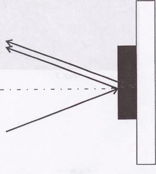
5 taken into account that even a topology with moderately dense graphics, with a line size of several microns will contain approximately 400,000 orderly arranged diffracting elements that will produce a diverse, ordered diffraction pattern. Orderliness will depend on whether all circumferences are built in compliance with the same law. The part of the substrate with uniform line density, i. e. filled with the circumferences of radius R, will evenly structure the field along the whole sector with uniform line density. Thus, the part of the substrate is evenly filled with lines of different radii without the "seams" that were used to generate quasi-uniform line density in the existing device and made the structuring of the electromagnetic field non-uniform. The set of attributes stated in cl. 2 of the Claims characterizes a device for structuring of electromagnetic field, where the substrate is made of silicon, and the topology is made of metal. The set of attributes stated in cl. 3 of the Claims characterizes a device for structuring of electromagnetic field, where the substrate is made of aluminum, and the topology is graphite. The choice of materials for the substrate and fractal topology is of great importance. Upon general consideration, efficiency of a diffraction structure will clearly be the longer, the greater the difference in their density is. Considerable difference in refraction ratio in every pair of the materials specified in cls. 2 and 3 of the Claims ensures distinctly pronounced diffraction pattern in both cases. The set of attributes stated in cl. 4 of the Claims characterizes a device for structuring of electromagnetic field, where the fractal topology is made up by slits with a width and depth of at least 1 mcm. The slits in the diffraction grating act as waveguides on which electromagnetic waves propagate. In the slits, there appears interference of several constant electromagnetic waves. The originating resonance phenomena lead to full refection of energy. The resonance phenomena influence the interference fringe pattern in the remote and near zones. This phenomenon can be interpreted as expansion of the near zone into the remote one. The minimal slit width, i. e. 0.1 mcm, is related to the covered spectral band of electromagnetic radiation (0.1 mcm is the UV wavelength). However, experiments show that even 7-mcm slits are sufficient to structure the whole optical spectrum. It can be explained by the fact that the minimal covered wavelength will depend not only on the slit parameters, but also on the dimensions of the most acute angle in the implemented fractal graphic. The minimal slit depth of 0.1 mcm is chosen empirically, by general physical consideration: the height of a step as of a diffracting element cannot be less than the wavelength of electromagnetic radiation. With that depth, the structured area reaches several centimeters. Creating a topology by means of slits is most efficient for producing a distinctly pronounced diffraction pattern. The set of attributes stated in cl. 5 of the Claims characterizes a device for structuring of electromagnetic field, where the topology is made of slits, and the substrate is made of polyvinyl. Such flexible structures can act as protective screens, for example, for cathode ray tube devices. The set of attributes specified in cl. 6 of the Claims characterizes a device where the topology is made of slits, and the substrate is a layered structure with the upper layer in the form of a semi-transparent reflective coating that ensures reflection from the lower layer. The semi-transparent reflection layer adds another structuring element. Each beam (Fig. З) hitting the coating will be reflected twice: first time from the outer surface, and second time upon entering the coating with refraction, from the borderline between the coating and the next layer. Thus, different wavelength bands will be reflected from every element of the structure. The reflected packet waves of different length from a large number of elements will interfere. The invention is illustrated by means of designs: Fig. 1 shows a device for structuring of electromagnetic field; Fig. 2 shows an example of origination of a topology. Fig. З shows a diagram of progress of beams for a device in the form of a layered structure; Figs. 4 and 5 are photographs of the structured electromagnetic field. Fig. 1 shows the type of topology generated by concentric circumferences, with each radius determined as R 2 n 1, where n is the ordinal number of the circumference. In this case the last circumference is the seventh. The topology is made on a substrate. Fig. 2 shows the initial stage of building a topology. The middle part of the substrate is filled with nine circumferences with a minimum radius equal to R; the center of each circumference is located on the neighboring circumference. The center of each of them is the center of seven concentric circumferences. The materials of the substrate and lines should have different refraction ratios. The more they differ from each other, the greater the structuring effect of the electromagnetic field will be. Consider an example of making a device where the topology is made up by slits. The slits are formed as follows. The substrate is coated, for instance, with a positive resist. The required pattern of graphics is formed within the layer, for example, by means of contact printing. Then a metal film is deposited. It is thinner than the resist layer. Then the resist is subjected to explosive lithography, where the resist along with the metal film on its surface are removed, and the metal film with the generated fractal topology remains on the substrate, the open parts of the substrate to undergo etching. The next stage is dry etching. The ratio of the slit depth to the width can be up to A device was manufactured where the substrate was made of glass, and the slits were 3 mcm wide and 2 mcm deep. Uniformly structured field extends for 3 cm from the substrate (Fig. 4). A device like the one above was also made, but the glass was additionally coated with a 0.1 mcm thick nickel film. The structured field extends for 4 cm from the substrate (Fig. 5). When the substrate was silicon, and the lines making up the matrix were made of aluminum, the structured electromagnetic field extends for 1 cm from the substrate. Experiments that confirm structuring of the electromagnetic field were conducted using a nonmonochromatic light source. Experiments reveal that the proposed device ensured uniform distribution of the electromagnetic field along the surface of the substrate sector where the topology is formed with uniform line density, and that effect is ensured by the uniform structure of the matrix. Patent Claims
6 7. A device for structuring of electromagnetic radiation in the wavebands between submicron and millimiter; it has a substrate bearing a topological layout containing an aggregate of concentric circumferences with each radius equal to R 2 n 1, where n is the ordinal number of the circumference from the center, characterized in that the topology is made in the form of an aggregate of circumferences with radius R, each of the circumferences is the geometric locus containing the same number of the centers of the neighboring circumferences; each of the centers located on the same circumference is at equal distances from the two neighboring ones, and each center of a circumference with radius R is the center of the same number of concentric circumferences, with each of their radius equal to R 2 n 1, where n max =7. 8. A device for structuring of electromagnetic radiation as per cl. 1 characterized in that the substrate is made of silicon, and the topology is made of metal. 9. A device for structuring of electromagnetic radiation as per cl. 1 characterized in that the substrate is made of aluminum, and the topology is graphite. 10. A device for structuring of electromagnetic radiation as per cl. 1 characterized in that the substrate is made up by slits with a width and depth of at least 1 mcm. 11. A device for structuring of electromagnetic radiation as per cl. 4 characterized in that the substrate is made of polyvinyl. 12. A device for structuring of electromagnetic radiation as per cl. 4 characterized in that the substrate is a layered structure with the upper layer in the form of a semi-transparent reflective coating that ensures reflection from the lower layer.

7 Fig. 2 Fig. 3
DEVICE FOR CONVERTING ELECTROMAGNETIC RADIATION TO A COHERENT FORM
 PATENT FOR INVENTION 2312384 DEVICE FOR CONVERTING ELECTROMAGNETIC RADIATION TO A COHERENT FORM Patentee(s): Igor Nikolayevich Serov (RU) Inventor(s): Igor Nikolayevich Serov (RU) Application 2006134068
Diffraction. Interference with more than 2 beams. Diffraction gratings. Diffraction by an aperture. Diffraction of a laser beam
 Diffraction Interference with more than 2 beams 3, 4, 5 beams Large number of beams Diffraction gratings Equation Uses Diffraction by an aperture Huygen s principle again, Fresnel zones, Arago s spot Qualitative
Chapters 1 & 2. Definitions and applications Conceptual basis of photogrammetric processing
 Chapters 1 & 2 Chapter 1: Photogrammetry Definitions and applications Conceptual basis of photogrammetric processing Transition from two-dimensional imagery to three-dimensional information Automation
Optics and Images. Lenses and Mirrors. Matthew W. Milligan
 Optics and Images Lenses and Mirrors Light: Interference and Optics I. Light as a Wave - wave basics review - electromagnetic radiation II. Diffraction and Interference - diffraction, Huygen s principle
Big League Cryogenics and Vacuum The LHC at CERN
 Big League Cryogenics and Vacuum The LHC at CERN A typical astronomical instrument must maintain about one cubic meter at a pressure of
DWDM FILTERS; DESIGN AND IMPLEMENTATION
 DWDM FILTERS; DESIGN AND IMPLEMENTATION 1 OSI REFERENCE MODEL PHYSICAL OPTICAL FILTERS FOR DWDM SYSTEMS 2 AGENDA POINTS NEED CHARACTERISTICS CHARACTERISTICS CLASSIFICATION TYPES PRINCIPLES BRAGG GRATINGS
Chapter Ray and Wave Optics
 109 Chapter Ray and Wave Optics 1. An astronomical telescope has a large aperture to [2002] reduce spherical aberration have high resolution increase span of observation have low dispersion. 2. If two
(A) 2f (B) 2 f (C) f ( D) 2 (E) 2
 2f (B) 2 f (C) f ( D) 2 (E) 2") 1. A small vibrating object S moves across the surface of a ripple tank producing the wave fronts shown above. The wave fronts move with speed v. The object is traveling in what direction and with what
1. A small vibrating object S moves across the surface of a ripple tank producing the wave fronts shown above. The wave fronts move with speed v. The object is traveling in what direction and with what
LOS 1 LASER OPTICS SET
 LOS 1 LASER OPTICS SET Contents 1 Introduction 3 2 Light interference 5 2.1 Light interference on a thin glass plate 6 2.2 Michelson s interferometer 7 3 Light diffraction 13 3.1 Light diffraction on a
GEOMETRICAL OPTICS Practical 1. Part I. BASIC ELEMENTS AND METHODS FOR CHARACTERIZATION OF OPTICAL SYSTEMS
 GEOMETRICAL OPTICS Practical 1. Part I. BASIC ELEMENTS AND METHODS FOR CHARACTERIZATION OF OPTICAL SYSTEMS Equipment and accessories: an optical bench with a scale, an incandescent lamp, matte, a set of
R.B.V.R.R. WOMEN S COLLEGE (AUTONOMOUS) Narayanaguda, Hyderabad.
 Narayanaguda, Hyderabad.") R.B.V.R.R. WOMEN S COLLEGE (AUTONOMOUS) Narayanaguda, Hyderabad. DEPARTMENT OF PHYSICS QUESTION BANK FOR SEMESTER III PAPER III OPTICS UNIT I: 1. MATRIX METHODS IN PARAXIAL OPTICS 2. ABERATIONS UNIT II
R.B.V.R.R. WOMEN S COLLEGE (AUTONOMOUS) Narayanaguda, Hyderabad. DEPARTMENT OF PHYSICS QUESTION BANK FOR SEMESTER III PAPER III OPTICS UNIT I: 1. MATRIX METHODS IN PARAXIAL OPTICS 2. ABERATIONS UNIT II
ABC Math Student Copy. N. May ABC Math Student Copy. Physics Week 13(Sem. 2) Name. Light Chapter Summary Cont d 2
 Name. Light Chapter Summary Cont d 2") Page 1 of 12 Physics Week 13(Sem. 2) Name Light Chapter Summary Cont d 2 Lens Abberation Lenses can have two types of abberation, spherical and chromic. Abberation occurs when the rays forming an image
Page 1 of 12 Physics Week 13(Sem. 2) Name Light Chapter Summary Cont d 2 Lens Abberation Lenses can have two types of abberation, spherical and chromic. Abberation occurs when the rays forming an image
Introduction Visible light is an electromagnetic wave, characterized by a wavelength, an amplitude
 Thin Film Interferences of SiO2 and TiO2 : Thickness and Iridescence Eman Mousa Alhajji North Carolina State University Department of Materials Science and Engineering MSE 355 Lab Report 201 A Matthew
N.N.Soboleva, S.M.Kozel, G.R.Lockshin, MA. Entin, K.V. Galichsky, P.L. Lebedinsky, P.M. Zhdanovich. Moscow Institute ofphysics and Technology
 Computer assisted optics teaching at the Moscow Institute ofphysics and Technology N.N.Soboleva, S.M.Kozel, G.R.Lockshin, MA. Entin, K.V. Galichsky, P.L. Lebedinsky, P.M. Zhdanovich Moscow Institute ofphysics
Supporting Information: Achromatic Metalens over 60 nm Bandwidth in the Visible and Metalens with Reverse Chromatic Dispersion
 Supporting Information: Achromatic Metalens over 60 nm Bandwidth in the Visible and Metalens with Reverse Chromatic Dispersion M. Khorasaninejad 1*, Z. Shi 2*, A. Y. Zhu 1, W. T. Chen 1, V. Sanjeev 1,3,
Chapter 17: Wave Optics. What is Light? The Models of Light 1/11/13
 Chapter 17: Wave Optics Key Terms Wave model Ray model Diffraction Refraction Fringe spacing Diffraction grating Thin-film interference What is Light? Light is the chameleon of the physical world. Under
Electromagnetic Radiation
 Electromagnetic Radiation EMR Light: Interference and Optics I. Light as a Wave - wave basics review - electromagnetic radiation II. Diffraction and Interference - diffraction, Huygen s principle - superposition,
INTRODUCTION THIN LENSES. Introduction. given by the paraxial refraction equation derived last lecture: Thin lenses (19.1) = 1. Double-lens systems
 = 1. Double-lens systems") Chapter 9 OPTICAL INSTRUMENTS Introduction Thin lenses Double-lens systems Aberrations Camera Human eye Compound microscope Summary INTRODUCTION Knowledge of geometrical optics, diffraction and interference,
Chapter 9 OPTICAL INSTRUMENTS Introduction Thin lenses Double-lens systems Aberrations Camera Human eye Compound microscope Summary INTRODUCTION Knowledge of geometrical optics, diffraction and interference,
Phys214 Fall 2004 Midterm Form A
 1. A clear sheet of polaroid is placed on top of a similar sheet so that their polarizing axes make an angle of 30 with each other. The ratio of the intensity of emerging light to incident unpolarized
Conceptual Physics Fundamentals
 Conceptual Physics Fundamentals Chapter 13: LIGHT WAVES This lecture will help you understand: Electromagnetic Spectrum Transparent and Opaque Materials Color Why the Sky is Blue, Sunsets are Red, and
Chapter Wave Optics. MockTime.com. Ans: (d)
") Chapter Wave Optics Q1. Which one of the following phenomena is not explained by Huygen s construction of wave front? [1988] (a) Refraction Reflection Diffraction Origin of spectra Q2. Which of the following
Chapter Wave Optics Q1. Which one of the following phenomena is not explained by Huygen s construction of wave front? [1988] (a) Refraction Reflection Diffraction Origin of spectra Q2. Which of the following
This writeup is adapted from Fall 2002, final project report for by Robert Winsor.
 Optical Waveguides in Andreas G. Andreou This writeup is adapted from Fall 2002, final project report for 520.773 by Robert Winsor. September, 2003 ABSTRACT This lab course is intended to give students
Lithography. 3 rd. lecture: introduction. Prof. Yosi Shacham-Diamand. Fall 2004
 Lithography 3 rd lecture: introduction Prof. Yosi Shacham-Diamand Fall 2004 1 List of content Fundamental principles Characteristics parameters Exposure systems 2 Fundamental principles Aerial Image Exposure
CHAPTER 7. Waveguide writing in optimal conditions. 7.1 Introduction
 CHAPTER 7 7.1 Introduction In this chapter, we want to emphasize the technological interest of controlled laser-processing in dielectric materials. Since the first report of femtosecond laser induced refractive
Mirrors and Lenses. Images can be formed by reflection from mirrors. Images can be formed by refraction through lenses.
 Mirrors and Lenses Images can be formed by reflection from mirrors. Images can be formed by refraction through lenses. Notation for Mirrors and Lenses The object distance is the distance from the object
Exercise 8: Interference and diffraction
 Physics 223 Name: Exercise 8: Interference and diffraction 1. In a two-slit Young s interference experiment, the aperture (the mask with the two slits) to screen distance is 2.0 m, and a red light of wavelength
Grating-waveguide structures and their applications in high-power laser systems
 Grating-waveguide structures and their applications in high-power laser systems Marwan Abdou Ahmed*, Martin Rumpel, Tom Dietrich, Stefan Piehler, Benjamin Dannecker, Michael Eckerle, and Thomas Graf Institut
The Method of Verifying an Authenticity of Printing Production. Samples
 1 The Method of Verifying an Authenticity of Printing Production Samples Abstract: The invention is related to protection of printed production against counterfeit using the technologies where the original
Chapter 18 Optical Elements
 Chapter 18 Optical Elements GOALS When you have mastered the content of this chapter, you will be able to achieve the following goals: Definitions Define each of the following terms and use it in an operational
MASSACHUSETTS INSTITUTE OF TECHNOLOGY. 2.71/2.710 Optics Spring 14 Practice Problems Posted May 11, 2014
 MASSACHUSETTS INSTITUTE OF TECHNOLOGY 2.71/2.710 Optics Spring 14 Practice Problems Posted May 11, 2014 1. (Pedrotti 13-21) A glass plate is sprayed with uniform opaque particles. When a distant point
End-of-Chapter Exercises
 End-of-Chapter Exercises Exercises 1 12 are conceptual questions designed to see whether you understand the main concepts in the chapter. 1. Red laser light shines on a double slit, creating a pattern
Unit Test Strand: The Wave Nature of Light
 22K 11T 2A 3C Unit Test Strand: The Wave Nature of Light Expectations: E1. analyse technologies that use the wave nature of light, and assess their impact on society and the environment; E2. investigate,
Diffractive interferometer for visualization and measurement of optical inhomogeneities
 Diffractive interferometer for visualization and measurement of optical inhomogeneities Irina G. Palchikova,2, Ivan А. Yurlagin 2 Technological Design Institute of Scientific Instrument Engineering (TDI
Supplementary Figure 1 Reflective and refractive behaviors of light with normal
 Supplementary Figures Supplementary Figure 1 Reflective and refractive behaviors of light with normal incidence in a three layer system. E 1 and E r are the complex amplitudes of the incident wave and
(51) Int Cl.: G01B 9/02 ( ) G01B 11/24 ( ) G01N 21/47 ( )
 Int Cl.: G01B 9/02 ( ) G01B 11/24 ( ) G01N 21/47 ( )") (19) (12) EUROPEAN PATENT APPLICATION (11) EP 1 939 581 A1 (43) Date of publication: 02.07.2008 Bulletin 2008/27 (21) Application number: 07405346.3 (51) Int Cl.: G01B 9/02 (2006.01) G01B 11/24 (2006.01)
(19) (12) EUROPEAN PATENT APPLICATION (11) EP 1 939 581 A1 (43) Date of publication: 02.07.2008 Bulletin 2008/27 (21) Application number: 07405346.3 (51) Int Cl.: G01B 9/02 (2006.01) G01B 11/24 (2006.01)
CHIRPED FIBER BRAGG GRATING (CFBG) BY ETCHING TECHNIQUE FOR SIMULTANEOUS TEMPERATURE AND REFRACTIVE INDEX SENSING
 BY ETCHING TECHNIQUE FOR SIMULTANEOUS TEMPERATURE AND REFRACTIVE INDEX SENSING") CHIRPED FIBER BRAGG GRATING (CFBG) BY ETCHING TECHNIQUE FOR SIMULTANEOUS TEMPERATURE AND REFRACTIVE INDEX SENSING Siti Aisyah bt. Ibrahim and Chong Wu Yi Photonics Research Center Department of Physics,
CHIRPED FIBER BRAGG GRATING (CFBG) BY ETCHING TECHNIQUE FOR SIMULTANEOUS TEMPERATURE AND REFRACTIVE INDEX SENSING Siti Aisyah bt. Ibrahim and Chong Wu Yi Photonics Research Center Department of Physics,
Invited Paper. recording. Yuri N. Denisyuk, Nina M. Ganzherli and Irma A. Maurer
 Invited Paper Thick-layered light-sensitive dichromated gelatin for 3D hologram recording Yuri N. Denisyuk, Nina M. Ganzherli and Irma A. Maurer loffe Physico-Technical Institute of the Academy of Sciences
Chapter 28 Physical Optics: Interference and Diffraction
 Chapter 28 Physical Optics: Interference and Diffraction 1 Overview of Chapter 28 Superposition and Interference Young s Two-Slit Experiment Interference in Reflected Waves Diffraction Resolution Diffraction
Physics 1520, Spring 2013 Quiz 2, Form: A
 Physics 1520, Spring 2013 Quiz 2, Form: A Name: Date: Section 1. Exercises 1. The index of refraction of a certain type of glass for red light is 1.52. For violet light, it is 1.54. Which color of light,
Electromagnetic Waves Chapter Questions
 Electromagnetic Waves Chapter Questions 1. Sir Isaac Newton was one of the first physicists to study light. What properties of light did he explain by using the particle model? 2. Who was the first person
Tutorial Zemax 9: Physical optical modelling I
 Tutorial Zemax 9: Physical optical modelling I 2012-11-04 9 Physical optical modelling I 1 9.1 Gaussian Beams... 1 9.2 Physical Beam Propagation... 3 9.3 Polarization... 7 9.4 Polarization II... 11 9 Physical
Sonic crystal noise barrier using locally resonant scatterers
 PROCEEDINGS of the 22 nd International Congress on Acoustics Road Traffic Noise Modeling and Noise Barrier: Paper ICA2016-904 Sonic crystal noise barrier using locally resonant scatterers Nicole Kessissoglou
Chapter 29: Light Waves
 Lecture Outline Chapter 29: Light Waves This lecture will help you understand: Huygens' Principle Diffraction Superposition and Interference Polarization Holography Huygens' Principle Throw a rock in a
Absentee layer. A layer of dielectric material, transparent in the transmission region of
 Glossary of Terms A Absentee layer. A layer of dielectric material, transparent in the transmission region of the filter, due to a phase thickness of 180. Absorption curve, absorption spectrum. The relative
High Performance Thin Film Optical Coatings Technical Reference Document 09/13. Coatings Capabilities. Heat Control - Hot Mirror Filters
 Heat Control - Hot Mirror Filters A hot mirror is in essence a thin film coating applied to substrates in an effort to reflect infra-red radiation either as a means to harness the reflected wavelengths
LECTURE 26: Interference
 ANNOUNCEMENT *Final: Thursday December 14, 2017, 1 PM 3 PM *Location: Elliot Hall of Music *Covers all readings, lectures, homework from Chapters 28.6 through 33. *The exam will be multiple choice. Be
Physics 248 Spring 2009 Lab 1: Interference and Diffraction
 Name Section Physics 248 Spring 2009 Lab 1: Interference and Diffraction Your TA will use this sheet to score your lab. It is to be turned in at the end of lab. You must clearly explain your reasoning
Chapter 36: diffraction
 Chapter 36: diffraction Fresnel and Fraunhofer diffraction Diffraction from a single slit Intensity in the single slit pattern Multiple slits The Diffraction grating X-ray diffraction Circular apertures
PHY 431 Homework Set #5 Due Nov. 20 at the start of class
 PHY 431 Homework Set #5 Due Nov. 0 at the start of class 1) Newton s rings (10%) The radius of curvature of the convex surface of a plano-convex lens is 30 cm. The lens is placed with its convex side down
Research Article A Polymer Film Dye Laser with Spatially Modulated Emission Controlled by Transversely Distributed Pumping
 Optical Technologies Volume 2016, Article ID 1548927, 4 pages http://dx.doi.org/10.1155/2016/1548927 Research Article A Polymer Film Dye Laser with Spatially Modulated Emission Controlled by Transversely
I. Optics. 1) A convex spherical mirror has a focal distance f =1cm. An object is placed 3cm away. What is the image position, i? [5 points.
 A convex spherical mirror has a focal distance f =1cm. An object is placed 3cm away. What is the image position, i? [5 points.") I. Optics 1) A convex spherical mirror has a focal distance f =1cm. An object is placed 3cm away. What is the image position, i? [5 points.] (1) 1.5 cm (2) 0.75 cm (3) 1.2 cm (4) 1.5 cm (5) 0.75 cm (6)
I. Optics 1) A convex spherical mirror has a focal distance f =1cm. An object is placed 3cm away. What is the image position, i? [5 points.] (1) 1.5 cm (2) 0.75 cm (3) 1.2 cm (4) 1.5 cm (5) 0.75 cm (6)
Shortened 3D Corner Reflector Antenna Dragoslav Dobričić, YU1AW
 Shortened 3D Corner Reflector Antenna Dragoslav Dobričić, YU1AW Abstract In this text two 3D corner reflector antenna modifications are described. The first modification is regarding the input impedance
ii) When light falls on objects, it reflects the light and when the reflected light reaches our eyes then we see the objects.
 When light falls on objects, it reflects the light and when the reflected light reaches our eyes then we see the objects.") Light i) Light is a form of energy which helps us to see objects. ii) When light falls on objects, it reflects the light and when the reflected light reaches our eyes then we see the objects. iii) Light
Light i) Light is a form of energy which helps us to see objects. ii) When light falls on objects, it reflects the light and when the reflected light reaches our eyes then we see the objects. iii) Light
The analysis of optical wave beams propagation in lens systems
 Journal of Physics: Conference Series PAPER OPEN ACCESS The analysis of optical wave beams propagation in lens systems To cite this article: I Kazakov et al 016 J. Phys.: Conf. Ser. 735 01053 View the
Rec. ITU-R P RECOMMENDATION ITU-R P PROPAGATION BY DIFFRACTION. (Question ITU-R 202/3)
") Rec. ITU-R P.- 1 RECOMMENDATION ITU-R P.- PROPAGATION BY DIFFRACTION (Question ITU-R 0/) Rec. ITU-R P.- (1-1-1-1-1-1-1) The ITU Radiocommunication Assembly, considering a) that there is a need to provide
Rec. ITU-R P.- 1 RECOMMENDATION ITU-R P.- PROPAGATION BY DIFFRACTION (Question ITU-R 0/) Rec. ITU-R P.- (1-1-1-1-1-1-1) The ITU Radiocommunication Assembly, considering a) that there is a need to provide
HUYGENS PRINCIPLE AND INTERFERENCE
 HUYGENS PRINCIPLE AND INTERFERENCE VERY SHORT ANSWER QUESTIONS Q-1. Can we perform Double slit experiment with ultraviolet light? Q-2. If no particular colour of light or wavelength is specified, then
Principles of Optics for Engineers
 Principles of Optics for Engineers Uniting historically different approaches by presenting optical analyses as solutions of Maxwell s equations, this unique book enables students and practicing engineers
Flat Top, Ultra-Narrow Band Pass Optical Filters Using Plasma Deposited Hard Oxide Coatings
 Flat Top, Ultra-Narrow Band Pass Optical Filters Using Plasma Deposited Hard Oxide Coatings Alluxa Engineering Staff September 2012 0 1 0.1 1 cav 2 cav 3 cav 4 cav 5 cav 0.01 0.001 635 636 637 638 639
The Wave Nature of Light
 The Wave Nature of Light Physics 102 Lecture 7 4 April 2002 Pick up Grating & Foil & Pin 4 Apr 2002 Physics 102 Lecture 7 1 Light acts like a wave! Last week we saw that light travels from place to place
College Physics II Lab 3: Microwave Optics
 ACTIVITY 1: RESONANT CAVITY College Physics II Lab 3: Microwave Optics Taner Edis with Peter Rolnick Spring 2018 We will be dealing with microwaves, a kind of electromagnetic radiation with wavelengths
Surface Topography and Alignment Effects in UV-Modified Polyimide Films with Micron Size Patterns
 CHINESE JOURNAL OF PHYSICS VOL. 41, NO. 2 APRIL 2003 Surface Topography and Alignment Effects in UV-Modified Polyimide Films with Micron Size Patterns Ru-Pin Pan 1, Hua-Yu Chiu 1,Yea-FengLin 1,andJ.Y.Huang
INDEX OF REFRACTION index of refraction n = c/v material index of refraction n
 INDEX OF REFRACTION The index of refraction (n) of a material is the ratio of the speed of light in vacuuo (c) to the speed of light in the material (v). n = c/v Indices of refraction for any materials
LIGHT. ENERGY FOR LIFE 2 Presented by- Ms.Priya
 LIGHT ENERGY FOR LIFE 2 Presented by- Ms.Priya VOCABULARY 1. Opaque 2. Transparent 3. Translucent 4. Refraction 5. Reflection 6. Ray 7. Image 8. Virtual image 9. Medium 10.Vacuum 11. Lens 12. Spectrum
CHAPTER 2 MICROSTRIP REFLECTARRAY ANTENNA AND PERFORMANCE EVALUATION
 43 CHAPTER 2 MICROSTRIP REFLECTARRAY ANTENNA AND PERFORMANCE EVALUATION 2.1 INTRODUCTION This work begins with design of reflectarrays with conventional patches as unit cells for operation at Ku Band in
PHYS 241 FINAL EXAM December 11, 2006
 1. (5 points) Light of wavelength λ is normally incident on a diffraction grating, G. On the screen S, the central line is at P and the first order line is at Q, as shown. The distance between adjacent
Image Formation. Light from distant things. Geometrical optics. Pinhole camera. Chapter 36
 Light from distant things Chapter 36 We learn about a distant thing from the light it generates or redirects. The lenses in our eyes create images of objects our brains can process. This chapter concerns
Laser Beam Analysis Using Image Processing
 Journal of Computer Science 2 (): 09-3, 2006 ISSN 549-3636 Science Publications, 2006 Laser Beam Analysis Using Image Processing Yas A. Alsultanny Computer Science Department, Amman Arab University for
25 cm. 60 cm. 50 cm. 40 cm.
 Geometrical Optics 7. The image formed by a plane mirror is: (a) Real. (b) Virtual. (c) Erect and of equal size. (d) Laterally inverted. (e) B, c, and d. (f) A, b and c. 8. A real image is that: (a) Which
SUPPLEMENTARY INFORMATION
 A transparent bending-insensitive pressure sensor Sungwon Lee 1,2, Amir Reuveny 1,2, Jonathan Reeder 1#, Sunghoon Lee 1,2, Hanbit Jin 1,2, Qihan Liu 5, Tomoyuki Yokota 1,2, Tsuyoshi Sekitani 1,2,3, Takashi
PRINCIPLE PROCEDURE ACTIVITY. AIM To observe diffraction of light due to a thin slit.
 ACTIVITY 12 AIM To observe diffraction of light due to a thin slit. APPARATUS AND MATERIAL REQUIRED Two razor blades, one adhesive tape/cello-tape, source of light (electric bulb/ laser pencil), a piece
Diffraction, Fourier Optics and Imaging
 1 Diffraction, Fourier Optics and Imaging 1.1 INTRODUCTION When wave fields pass through obstacles, their behavior cannot be simply described in terms of rays. For example, when a plane wave passes through
Spectrophotometer. An instrument used to make absorbance, transmittance or emission measurements is known as a spectrophotometer :
 Spectrophotometer An instrument used to make absorbance, transmittance or emission measurements is known as a spectrophotometer : Spectrophotometer components Excitation sources Deuterium Lamp Tungsten
Physics 197 Lab 8: Interference
 Physics 197 Lab 8: Interference Equipment: Item Part # per Team # of Teams Bottle of Bubble Solution with dipper 1 8 8 Wine Glass 1 8 8 Straw 1 8 8 Optics Bench PASCO OS-8518 1 8 8 Red Diode Laser and
Effects of Photographic Gamma on Hologram Reconstructions*
 1650 JOURNAL OF THE OPTICAL SOCIETY OF AMERICA VOLUME 59. NUMBER 12 DECEMBER 1969 Effects of Photographic Gamma on Hologram Reconstructions* J AMES C. WYANT AND M. PA RKER G IVENS The Institute of Optics,
Basic Optics System OS-8515C
 40 50 30 60 20 70 10 80 0 90 80 10 20 70 T 30 60 40 50 50 40 60 30 70 20 80 90 90 80 BASIC OPTICS RAY TABLE 10 0 10 70 20 60 50 40 30 Instruction Manual with Experiment Guide and Teachers Notes 012-09900B
Module - 2 Lecture - 13 Lithography I
 Nano Structured Materials-Synthesis, Properties, Self Assembly and Applications Prof. Ashok. K.Ganguli Department of Chemistry Indian Institute of Technology, Delhi Module - 2 Lecture - 13 Lithography
Will contain image distance after raytrace Will contain image height after raytrace
 Name: LASR 51 Final Exam May 29, 2002 Answer all questions. Module numbers are for guidance, some material is from class handouts. Exam ends at 8:20 pm. Ynu Raytracing The first questions refer to the
Waveguiding in PMMA photonic crystals
 ROMANIAN JOURNAL OF INFORMATION SCIENCE AND TECHNOLOGY Volume 12, Number 3, 2009, 308 316 Waveguiding in PMMA photonic crystals Daniela DRAGOMAN 1, Adrian DINESCU 2, Raluca MÜLLER2, Cristian KUSKO 2, Alex.
COUPLED SECTORIAL LOOP ANTENNA (CSLA) FOR ULTRA-WIDEBAND APPLICATIONS *
 FOR ULTRA-WIDEBAND APPLICATIONS *") COUPLED SECTORIAL LOOP ANTENNA (CSLA) FOR ULTRA-WIDEBAND APPLICATIONS * Nader Behdad, and Kamal Sarabandi Department of Electrical Engineering and Computer Science University of Michigan, Ann Arbor, MI,
COUPLED SECTORIAL LOOP ANTENNA (CSLA) FOR ULTRA-WIDEBAND APPLICATIONS * Nader Behdad, and Kamal Sarabandi Department of Electrical Engineering and Computer Science University of Michigan, Ann Arbor, MI,
Experiment 1: Fraunhofer Diffraction of Light by a Single Slit
 Experiment 1: Fraunhofer Diffraction of Light by a Single Slit Purpose 1. To understand the theory of Fraunhofer diffraction of light at a single slit and at a circular aperture; 2. To learn how to measure
A process for, and optical performance of, a low cost Wire Grid Polarizer
 1.0 Introduction A process for, and optical performance of, a low cost Wire Grid Polarizer M.P.C.Watts, M. Little, E. Egan, A. Hochbaum, Chad Jones, S. Stephansen Agoura Technology Low angle shadowed deposition
Raman images constructed from. Raman Imaging: Defining the Spatial Resolution of the Technology
 18 Raman Technology for Today s Spectroscopists June 26 Raman Imaging: Defining the Spatial Resolution of the Technology Chemical images of polystyrene beads on silicon acquired using Raman mapping and
Module 19 : WDM Components
 Module 19 : WDM Components Lecture : WDM Components - I Part - I Objectives In this lecture you will learn the following WDM Components Optical Couplers Optical Amplifiers Multiplexers (MUX) Insertion
MASSACHUSETTS INSTITUTE OF TECHNOLOGY Department of Electrical Engineering and Computer Science
 Student Name Date MASSACHUSETTS INSTITUTE OF TECHNOLOGY Department of Electrical Engineering and Computer Science 6.161 Modern Optics Project Laboratory Laboratory Exercise No. 3 Fall 2005 Diffraction
Physical Optics. Diffraction.
 Physical Optics. Diffraction. Interference Young s interference experiment Thin films Coherence and incoherence Michelson interferometer Wave-like characteristics of light Huygens-Fresnel principle Interference.
Technical Notes. Introduction. Optical Properties. Issue 6 July Figure 1. Specular Reflection:
 Technical Notes This Technical Note introduces basic concepts in optical design for low power off-grid lighting products and suggests ways to improve optical efficiency. It is intended for manufacturers,
A thin foil optical strain gage based on silicon-on-insulator microresonators
 A thin foil optical strain gage based on silicon-on-insulator microresonators D. Taillaert* a, W. Van Paepegem b, J. Vlekken c, R. Baets a a Photonics research group, Ghent University - INTEC, St-Pietersnieuwstraat
Advanced Features of InfraTec Pyroelectric Detectors
 1 Basics and Application of Variable Color Products The key element of InfraTec s variable color products is a silicon micro machined tunable narrow bandpass filter, which is fully integrated inside the
The diffraction of light
 7 The diffraction of light 7.1 Introduction As introduced in Chapter 6, the reciprocal lattice is the basis upon which the geometry of X-ray and electron diffraction patterns can be most easily understood
General Physics II. Ray Optics
 General Physics II Ray Optics 1 Dispersion White light is a combination of all the wavelengths of the visible part of the electromagnetic spectrum. Red light has the longest wavelengths and violet light
Major Fabrication Steps in MOS Process Flow
 Major Fabrication Steps in MOS Process Flow UV light Mask oxygen Silicon dioxide photoresist exposed photoresist oxide Silicon substrate Oxidation (Field oxide) Photoresist Coating Mask-Wafer Alignment
is a method of transmitting information from one place to another by sending light through an optical fiber. The light forms an electromagnetic
 is a method of transmitting information from one place to another by sending light through an optical fiber. The light forms an electromagnetic carrier wave that is modulated to carry information. The
Lecture Outline Chapter 28. Physics, 4 th Edition James S. Walker. Copyright 2010 Pearson Education, Inc.
 Lecture Outline Chapter 28 Physics, 4 th Edition James S. Walker Chapter 28 Physical Optics: Interference and Diffraction Units of Chapter 28 Superposition and Interference Young s Two-Slit Experiment
Spatial-Phase-Shift Imaging Interferometry Using Spectrally Modulated White Light Source
 Spatial-Phase-Shift Imaging Interferometry Using Spectrally Modulated White Light Source Shlomi Epshtein, 1 Alon Harris, 2 Igor Yaacobovitz, 1 Garrett Locketz, 3 Yitzhak Yitzhaky, 4 Yoel Arieli, 5* 1AdOM
Examination Optoelectronic Communication Technology. April 11, Name: Student ID number: OCT1 1: OCT 2: OCT 3: OCT 4: Total: Grade:
 Examination Optoelectronic Communication Technology April, 26 Name: Student ID number: OCT : OCT 2: OCT 3: OCT 4: Total: Grade: Declaration of Consent I hereby agree to have my exam results published on
Slide 1 / 99. Electromagnetic Waves
 Slide 1 / 99 Electromagnetic Waves Slide 2 / 99 The Nature of Light: Wave or Particle The nature of light has been debated for thousands of years. In the 1600's, Newton argued that light was a stream of
StarBright XLT Optical Coatings
 StarBright XLT Optical Coatings StarBright XLT is Celestron s revolutionary optical coating system that outperforms any other coating in the commercial telescope market. Our most popular Schmidt-Cassegrain
EE-527: MicroFabrication
 EE-57: MicroFabrication Exposure and Imaging Photons white light Hg arc lamp filtered Hg arc lamp excimer laser x-rays from synchrotron Electrons Ions Exposure Sources focused electron beam direct write
National 3 Physics Waves and Radiation. 1. Wave Properties
 1. Wave Properties What is a wave? Waves are a way of transporting energy from one place to another. They do this through some form of vibration. We see waves all the time, for example, ripples on a pond
Angela Piegari ENEA, Optical Coatings Laboratory, Roma, Italy
 Optical Filters for Space Instrumentation Angela Piegari ENEA, Optical Coatings Laboratory, Roma, Italy Trieste, 18 February 2015 Optical Filters Optical Filters are commonly used in Space instruments