MIC4223/MIC4224/MIC4225
|
|
|
- Bertram Dorsey
- 5 years ago
- Views:
Transcription
1 Dual 4A, 4.5V to 18V, 15ns Switch Time, Low-Side MOSFET Drivers with Enable General Description The are a family of a dual 4A, High-Speed, Low-side MOSFET drivers with logic-level driver enables. The devices are fabricated on Micrel s Bipolar/CMOS/DMOS (BCD) process and operate from a 4.5V to 18V supply voltage. The devices parallel Bipolar and CMOS output stage architecture provides high-current throughout the MOSFETs Miller Region allowing the driver to sink and source 4A of peak current from a 12V supply and quickly charge and discharge a 2pF load capacitance in under 15ns, while allowing the outputs to swing within.3v of V DD and.16v of ground. The driver and enable inputs feature TTL and CMOS logic-level thresholds which are independent of supply voltage. Each driver features a dedicated active-high enable input which is internally pulled high to V DD through 1kΩ, allowing the pins to be left unconnected if it is not required to disable the driver outputs. The driver inputs have been designed to protect against ground bounce and are protected to withstand -5V of voltage swing at -4mA. Driver outputs are also protected to withstand 5mA of reverse current. The are available in three configurations using industry standard pin out; dual inverting (MIC4223), dual non-inverting (MIC4224) and complimentary (MIC4225). They are available in 8-pin SOIC and thermally enhanced e-pad 8-pin MSOP and support operating junction temperatures from -4 C to +125 C. Applications High-Efficiency MOSFET switching Switch mode power supplies DC-to-DC converters Motor and solenoid drivers Clock and line drivers Synchronous rectifiers Pulse transformer drive Class D switching amplifiers Features 4.5V to 18V supply voltage operating range High peak source/sink current ±3A at V DD = 8V ±4A at V DD = 12V 15ns/15ns Rise and Fall times with 2pF load 25ns/35ns (Rising/Falling) input propagation delay 2ns/45ns (Rising/Falling) enable propagation delay Active-high driver enable inputs with 1kΩ pull-ups CMOS and TTL logic input and enable thresholds independent of supply voltage Driver input protection to -5V at -4mA Output Latch-up protection to >5mA reverse current Industry standard pin out with two package options epad MSOP-8 (θ JA = 6 C/W) 8-pin SOIC (θ JA = 12 C/W) Available in dual-inverting (MIC4223), dual noninverting (MIC4224) and complementary (MIC4225) Dual output drive by paralleling channels -4 C to +125 C operating junction temperature range Block Diagram Micrel Inc. 218 Fortune Drive San Jose, CA USA tel +1 (48) fax + 1 (48) June 29 M A (48) 944-8
2 Ordering Information Part Number Configuration Junction Temp. Range Package Lead Finish MIC4223YM Dual Inverting 4 to +125 C 8-pin SOIC Pb-Free MIC4223YMME Dual Inverting 4 to +125 C 8-pin EPAD-MSOP Pb-Free MIC4224YM Dual Non-inverting 4 to +125 C 8-pin SOIC Pb-Free MIC4224YMME Dual Non-inverting 4 to +125 C 8-pin EPAD-MSOP Pb-Free MIC4225YM Inverting + Non-inverting 4 to +125 C 8-pin SOIC Pb-Free MIC4225YMME Inverting + Non-inverting 4 to +125 C 8-pin EPAD-MSOP Pb-Free Pin Configuration 8-Pin SOIC (YM) 8-Pin epad MSOP (YMME) 8-Pin SOIC (YM) 8-Pin epad MSOP (YMME) 8-Pin SOIC (YM) 8-Pin epad-msop (YMME) Pin Description Pin Number Pin Name Pin Function 1 ENA Enable pin for output A. TTL/CMOS-compatible logic input. A logic-level high enables the device. An internal pull-up enables the part if pin is open. A logic-level low disables the device and the output will be low regardless of the input state. 2 INA Control Input A: TTL/CMOS-compatible logic input. Connect to V DD or ground if not used and connect ENA to ground to disable driver A. 3 GND Ground 4 INB Control Input B: TTL/CMOS compatible logic input. Connect to V DD or ground if not used and connect ENB to ground to disable driver B. 5 OUTB Output B: Parallel Bipolar/CMOS output. 6 VDD Voltage Supply Input: +4.5V to +18V 7 OUTA Output A: Parallel Bipolar/CMOS output. 8 ENB Enable pin for output B. TTL/CMOS-compatible logic input. A logic-level high enables the device. An internal pull-up enables the part if pin is open. A logic-level low disables the device and the output will be low regardless of the input state. EP GND Exposed thermal pad for epad MSOP package only (Not available on SOIC-8L package). Connect to ground. Must make a full connection to the ground plane to maximize thermal performance of the package. June 29 2 M A (48) 944-8
3 Absolute Maximum Ratings (1) Supply Voltage (V DD )...+2V Input Voltage (V INA, V INB )... V DD +.3V to GND - 5V Enable Voltage (V ENA, V ENB ) V to V DD +.3V Junction Temperature (T J ) C to +15 C Storage Temperature C to +15 C Lead Temperature (1 sec.)... 3 C ESD Rating... HBM = 2kV, MM = 2V (3) Operating Ratings (2) Supply Voltage (V DD ) V to +18V Junction Temperature (T J )... 4 C to +125 C Package Thermal Resistance EPAD MSOP (θ JA )...6 C/W SOIC (θ JA )...12 C/W Electrical Characteristics 4.5V V DD 18V; C L = 2pF. T A = 25 C, bold values indicate full operating junction temperature range, unless noted. Symbol Parameter Condition Min Typ Max Units Input V IH Logic 1 Input Voltage V V IL Logic Input Voltage V Hysteresis.25 V I IN Input Current V IN V DD 1 1 µa 1 1 µa V IN = -5V -4 ma Output V OH High Output Voltage I OUT = -1mA, V DD = 18V V DD -.45 V V OL Low Output Voltage I OUT = 1mA, V DD = 18V.3 V RO Output Resistance Source Output Resistance Sink Peak Output Current I OUT = -1mA, V DD = 18V I OUT = 1mA, V DD = 18V IPK V DD = 8V ±3 A V DD = 12V ±4 I Latch-Up Protection Withstand reverse current >5 ma Switching Time t R Rise Time Test Figure 1; C L = 2pF 15 4 ns t F Fall Time Test Figure 1; C L = 2pF 15 4 ns t D1 Delay Time Test Figure 1; C L = 2pF ns t D2 Delay Time Test Figure 1; C L = 2pF 35 5 ns Enable (ENA, ENB) V EN_H High Level Enable Voltage LO to HI transition V V EN_L Low Level Enable Voltage HI to LO transition V Hysteresis.35 V R EN Enable Impedance V DD = 18V, V ENA = V ENB = GND 1 kω t D3 Propagation Delay Time C L = 2pF 2 6 ns t D4 Propagation Delay Time C L = 2pF ns Power Supply I SH Power Supply Current V INA = V INB = 3.V, V ENA = V ENB = open ma I SL Power Supply Current V INA = V INB =.V, V ENA = V ENB = open ma Notes: 1. Exceeding the absolute maximum rating may damage the device. 2. The device is not guaranteed to function outside its operating rating. 3. Devices are ESD sensitive. Handling precautions recommended. Human body model, 1.5kΩ in series with 1pF Ω June 29 3 M A (48) 944-8
4 Test Circuit Figure 1. Test Circuit Timing Diagram Inverting Driver Non-Inverting Driver Enable to Output Timing Diagram June 29 4 M A (48) 944-8
5 Typical Characteristics Conditions: T A =25ºC. Threshold (V) V INA, B Threshold vs. V DD Enable Threshold vs. Temperature V DD =12V V IH V IL V EN_H V EN_L I DD vs. Temperature (Disabled) V DD = 12; V IN = V DD V DD = 4.5V; V IN = V DD V DD = 12V; V IN = V DD = 4.5V; V IN = I DD vs. Frequency (V DD = 5V) Both Drivers Switching 2.2nF 1nF 47pF Frequency (khz) Threshold (V) V INA, B Threshold vs. Temperature V DD =12V I DD vs. V DD (Disabled) V INA = V INB = V DD I DD vs. Temperature (Enabled) V DD = 12; V IN = V DD V DD = 4.5; V IN = V DD V DD = 4.5V; V IN = V DD = 12; V IN = V IL V IH V INA = V INB = I DD vs. Frequency (V DD = 5V) Both Drivers Switching 1nF 4.7nF Frequency (khz) V ENA, B Threshold vs. V DD V EN_H V EN_L I DD vs. V DD (Enabled) V INA = V INB = V DD V INA = V INB = I DD vs. Temperature (Switching) V DD = 12V; V IN = 5kHz V DD = 4.5V; V IN = 5kHz I DD vs. Frequency (V DD = 12V) Both Drivers Switching 2.2nF 1nF 47pF Frequency (khz) June 29 5 M A (48) 944-8
6 Conditions: T A = 25ºC I DD vs. Frequency (V DD = 12V) Both Drivers Switching 1nF 4.7nF Frequency (khz) I DD vs. V DD (C L = 2.2nF) Both Drivers Switching 2kHz 1kHz 5kHz I DD vs. V DD (C L = 2.2nF) Both Drivers Switching 2MHz 1MHz 5kHz I DD vs. V DD (C L = 4.7nF) Both Drivers Switching 2kHz 1kHz 5kHz I DD vs. V DD (C L = 4.7nF) Both Drivers Switching 2MHz 1MHz 5kHz Output Rise Time (ns) Output Rise Time vs. V DD 2.2nF 1nF 47pF Output Rise Time (ns) Output Rise Time vs. V DD 1nF 4.7nF Output Fall Time (ns) Output Fall Time vs. V DD 2.2nF 1nF 47pF Output Fall Time (ns) Output Fall Time vs. V DD 1nF 4.7nF Propagation Delay (t D1 ) Propagation Delay (t D1 ) Propagation Delay (t D2 ) 3 vs. V DD 35 vs. V DD 3 vs. V DD Propagation Delay (ns) nF 47pF 1nF Propagation Delay (ns) nF 4.7nF Propagation Delay (ns) nF 1nF 47pF June 29 6 M A (48) 944-8
7 Conditions: T A = 25ºC. Propagation Delay (ns) Propagation Delay (t D2 ) vs. V DD 1nF 4.7nF Resistance (Ω) Output Source Resistance vs. Temperature I DD = 1mA V DD = 4.5V V DD = 12V V DD = 18V Resistance (Ω) Output Sink Resistance vs. Temperature I DD = 1mA V DD = 4.5V V DD = 12V V DD = 18V Output Rise Time vs. Temperature Output Fall Time vs. Temperature Prop. Delay (Inverting) vs. Temperature Output Rise Time (ns) C L = 2nF V DD = 18V V DD = 4.5V V DD = 12V Output Fall Time (ns) C L = 2nF V DD = 18V V DD = 4.5V V DD = 12V Delay (ns) C L = 2nF V DD = 12V; t D1 V DD = 4.5V; t D2 V DD = 4.5V; t D1 V DD = 12V; t D Delay (ns) Prop. Delay (Non-Inverting) vs. Temperature C L = 2nF V DD = 4.5V; t D2 V DD = 12V; t D1 V DD = 4.5V; t D1 V DD = 12V; t D Prop. Delay (ns) Enable to Output Delay (t D3 ) vs. Temperature C L = 2nF V DD = 4.5V V DD = 12V V DD = 18V Prop. Delay (ns) Enable to Output Delay (t D4 ) vs. Temperature C L = 2nF V DD = 4.5V V DD = 18V V DD = 12V June 29 7 M A (48) 944-8
8 Functional Diagram Logic Table Enables Inputs MIC4223 MIC4224 MIC4225 ENA ENB INA INB OUTA OUTB OUTA OUTB OUTA OUTB H H L L H H L L H L H H L H H L L H H H H H H L L H H L L L H H H H L L H H L H L L X X L L L L L L Block Diagram June 29 8 M A (48) 944-8
9 Functional Description The MIC4223, MIC4224 and MIC4225 are a family of dual high speed, high current drivers. The drivers come in both inverting and non-inverting versions. Each driver has an enable pin that turns the output off (low) regardless of the input. The MIC4223 is a dual inverting driver. The MIC4224 is a dual non-inverting driver and the MIC4225 contains an inverting and non-inverting driver. Enable Each output has an independent enable pin that forces the output low when the enable pin is driven low. Each enable pin is internally pulled-up to V DD. The outputs are enabled by default if the enable pin is left open. Pulling the enable pin low, below its threshold voltage, forces the output low. A fast propagation delay between the enable and output pins quickly disables the output, which is a requirement during a system fault condition. Input Stage The driver input stage is high impedance, TTL-compatible input stage. The driver s input threshold voltage makes it compatible with TTL and CMOS devices that are powered from supply voltages between 3V and V DD. Hysteresis on the input pin improves noise immunity and prevents input signals with slow rise times from falsely triggering the output. The VDD pin current is slightly higher when the input voltage is above the high level threshold. See the Typical Characteristic graphs for additional information. The input voltage signal may go up to -5V below ground without damage to the driver or cause a latch up condition. Negative input voltages that are.7v below ground or greater will increase propagation delay. Figure 2. Output Driver The slew rate of the output is non-adjustable and depends only on the V DD voltage and how much capacitance is present at the OUTA, B pin. Changing the slew rate at the driver s input pin will not affect the output rise or fall times. The slew rate at the MOSFET gate can be adjusted by adding a resistor between the MOSFET gate and the driver output. Output Driver Section A functional diagram of the driver output is shown in Figure 2. The output drive is a parallel combination of MOSFET and Bipolar transistor. For a given silicon area, a bipolar device has a lower on-resistance than an equivalent MOS device. It sources and sinks current more consistently as the voltage across it changes. The low drive impedance of the bipolar allows fast turn-on and turn-off of the external MOSFET. The driver s internal MOSFET gives the output near rail-to-rail drive capability. This ensures a low R DSON for the external MOSFET as well as noise immunity from dv/dt induced glitching. June 29 9 M A (48) 944-8
10 Application Information Power Dissipation Considerations Power dissipation in the driver can be separated into two areas: Output driver stage dissipation Quiescent current dissipation used to supply the internal logic and control functions. Output Driver Stage Power Dissipation Power dissipation in the driver s output stage is mainly caused by charging and discharging the gate to source and gate to drain capacitance of the external MOSFET. Figure 3 shows a simplified circuit of the MIC4223 driving an external MOSFET. Figure 4. MOSFET Gate Charge vs. V GS The energy dissipated during turn-on is calculated as: 1 2 E = 2 Ciss VGS where C is the MOSFET's total gate capacitance iss Figure 3. Functional MOSFET/Driver Diagram Dissipation Caused by Switching the External MOSFET Energy from capacitor C VDD is used to charge up the input capacitance of the MOSFET (C GD and C GS ). The energy delivered to the MOSFET is dissipated in the upper driver MOSFET and Bipolar impedances. The effective capacitance of C GD and C GS is difficult to calculate since they vary non-linearly with I D, V GS, and V DS. Fortunately, most power MOSFET specifications include a typical graph of total gate charge vs. V GS. Figure 4 shows a typical MOSFET gate charge curve. The graph illustrates that for a gate voltage of 1V, the MOSFET requires about 23.5nC of charge. but : Q = C V so E = 1/2 Q G V GS An equivalent amount of energy is dissipated in the driver s sink circuit when the MOSFET turns off. The total energy and power dissipated by the drive components is: E and P DRIVER DRIVER = Q = Q G G V V GS GS f S Where: E DRIVER is the energy dissipated per switching cycle P DRIVER is the power dissipated by switching the MOSFET on and off Q G is the total Gate charge at V GS V GS is the MOSFETs Gate to Source voltage f S is the switching frequency of the Gate drive circuit June 29 1 M A (48) 944-8
11 Quiescent Current Power Dissipation Quiescent current powers the internal logic, level shifting circuitry and bias for the output drivers. This current is proportional to operating frequency and V DD voltage. The typical characteristic graphs show how supply current varies with switching frequency and supply voltage. The power dissipated by the driver s quiescent current is: Pdiss = V I quiescent DD DD Total Power Dissipation and Thermal Considerations Total package power dissipation equals the power dissipation of each driver caused by driving the external MOSFETs plus the supply current. Pdiss = Pdiss + Pdriver + Pdriver TOTAL quiescent The die temperature may be calculated once the total power dissipation is known. T = T + Pdiss θ J A TOTAL Where: T A is the Maximum ambient temperature T J is the junction temperature ( C) Pdiss TOTAL is the power dissipation of the Driver θ JA is the thermal resistance from junction-toambient air ( C/W) The following graphs help determine the maximum gate charge that can be driven with respect to switching frequency, supply voltage and ambient temperature. Figure 5a shows the power dissipation in the driver for different values of gate charge with V DD = 5V. Figure 5b shows the power dissipation at V DD = 12V. Figure 5c show the maximum power dissipation for a given ambient temperature for the SOIC and epad MSOP packages. The maximum operating frequency of the driver may be limited by the maximum power dissipation of the driver package. JA A B PDISS (W) k PDISS: GATE Charge vs. Frequency V DD =5V 1M FREQUENCY (Hz) 5nC 4nC 3nC 2nC 1nC 1M Figure 5a. P DISS vs. Q G and f S for V DD = 5V PDISS (W) k PDISS: GATE Charge vs. Frequency V DD =12V 5nC 1M FREQUENCY (Hz) 4nC 3nC 2nC 1nC 1M Figure 5b. P DISS vs. Q G and f S for V DD = 12V Maximum Power Dissipation 2. Power Dissipation (W) Ambient Figure 5c. Maximum P DISS vs. Ambient Temperature June M A (48) 944-8
12 Bypass Capacitor Selection Bypass capacitors are required for proper operation by supplying the charge necessary to drive the external MOSFETs as well as minimize the voltage ripple on the supply pins. Ceramic capacitors are recommended because of their low impedance and small size. Z5U type ceramic capacitor dielectrics are not recommended due to the large change in capacitance over temperature and voltage. Manufacturer specifications should be checked to insure voltage and temperature do not reduce the capacitance below the value needed. A minimum value of 1µF is required regardless of the MOSFETs being driven. Larger MOSFETs, with their higher input capacitance may require larger decoupling capacitance values for proper operation. The voltage rating of the capacitors depends on the supply voltage, ambient temperature and the voltage derating used for reliability. Placement of the decoupling capacitors is critical. The bypass capacitor for V DD should be placed as close as possible between the VDD and GND pins. The etch connections must be short, wide and direct. The use of a ground plane to minimize connection impedance is recommended. Multiple vias insure a low inductance path and help with power dissipation. Refer to the section on layout and component placement for more information. Grounding, Component Placement and Circuit Layout Nanosecond switching speeds and ampere peak currents in and around the MOSFET driver necessitate proper placement and trace routing of all components. Improper placement may cause degraded noise immunity, false switching and excessive ringing. Figure 6 shows the critical current paths when the driver outputs go high and turn on the external MOSFETs. It also helps demonstrate the need for a low impedance ground plane. Charge needed to turn-on the MOSFET gates comes from the decoupling capacitors C VDD. Current in the gate driver flows from C VDD through the internal driver, into the MOSFET gate and out the Source. The return connection back to the decoupling capacitor is made through the ground plane. Any inductance or resistance in the ground return path causes a voltage spike or ringing to appear on the source of the MOSFET. This voltage works against the gate drive voltage and can either slow down or turn off the MOSFET during the period where it should be turned on. Figure 6. Driver Turn-On Current Path Figure 7 shows the critical current paths when the driver outputs go low and turn off the external MOSFETs. Short, low impedance connections are important during turn-off for the same reasons given in the turn-on explanation. Current from the V DD supply replenishes charge in the decoupling capacitor, C VDD. Figure 7. Driver Turn-Off Current Path The following circuit guidelines should be adhered to for optimum circuit performance: The V DD bypass capacitor must be placed close to the VDD and ground pins. It is critical that the etch length between the decoupling capacitor and the VDD and GND pins be minimized to reduce pin inductance. Multiple vias in parallel help minimize inductance in the ground and V DD paths. A ground plane is recommended to minimize parasitic inductance and impedance of the return paths. The MIC4223 family of drivers is capable of high peak currents and very fast transition times. Any impedance between the driver, the decoupling capacitors and the external MOSFET will degrade the performance of the circuit. Trace out the high di/dt and dv/dt paths, as shown in Figures 6 and 7 and minimize etch length and loop area for these connections. Minimizing these parameters decreases the parasitic inductance and the radiated EMI generated by fast rise and fall times. June M A (48) 944-8
13 Evaluation Board Schematic (SOIC) SOIC Package June M A (48) 944-8
14 Bill of Materials (SOIC) Item Part Number Manufacturer Description Qty. C1 VJ63Y14KXXAT Vishay (1).1µF/25V, X7R Ceramic Capacitor, Size 63 1 C2, C7 C168X5R1E15M TDK (2) 1µF/25V, X5R, Ceramic Capacitor, Size 63 2 or 633D15MAT AVX (3) 1µF/25V, X5R, Ceramic Capacitor, Size 63 2 or GRM188R61E15KA93 MuRata (4) 1µF/25V, X5R, Ceramic Capacitor, Size 63 2 C4, C5 C3216X7R1E15K TDK (2) 1µF/25V, X7R, Ceramic Capacitor, Size or 1263D15MAT AVX (3) 1µF/25V, X7R, Ceramic Capacitor, Size or GRM31MR71H15KA1 MuRata (4) 1µF/25V, X7R, Ceramic Capacitor, Size Q1, Q2 Si4174DY Vishay (1) 3V N-Channel MOSFET 2 C3, Open location Size 63 R4, C6, R9, R1, R2, R6, R8 R5, R7 CRCW12611FRT1 Vishay (1) 1kΩ Resistor, Size U1 MIC4223YM Micrel, Inc. (5) Dual Inverting 4A MOSFET Driver with SOIC Package 1 or MIC4224YM Micrel, Inc. (5) Dual Non-Inverting 4A MOSFET Driver with SOIC Package 1 or MIC4225YM Micrel, Inc. (5) Dual Inverting/Non-Inverting 4A MOSFET Driver with SOIC 1 Package Notes: 1. Vishay: 2. TDK: 3. AVX: 4. MuRata: 5. Micrel, Inc: June M A (48) 944-8


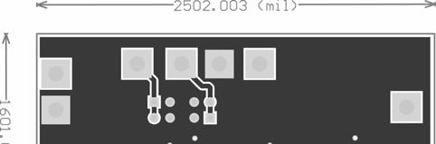
15 PCB Layout (SOIC) June M A (48) 944-8
16 Evaluation Board Schematic (e-pad MSOP) epad MSOP June M A (48) 944-8

")

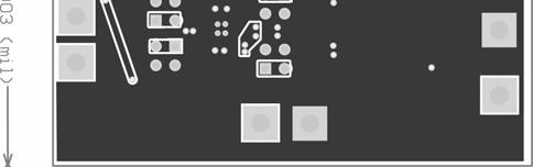
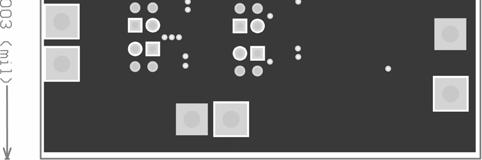
17 PCB Layout (epad MSOP) June M A (48) 944-8
18 Bill of Materials (epad MSOP) Item Part Number Manufacturer Description Qty. C1 VJ63Y14KXXAT Vishay (1).1µF/25V, X7R Ceramic Capacitor, Size 63 1 C2, C7 C168X5R1E15M TDK (2) 1µF/25V, X5R, Ceramic Capacitor, Size 63 2 or 633D15MAT AVX (3) 1µF/25V, X5R, Ceramic Capacitor, Size 63 2 or GRM188R61E15KA93 MuRata (4) 1µF/25V, X5R, Ceramic Capacitor, Size 63 2 C4, C5 C3216X7R1E15K TDK (2) 1µF/25V, X7R, Ceramic Capacitor, Size or 1263D15MAT AVX (3) 1µF/25V, X7R, Ceramic Capacitor, Size 2 or GRM31MR71H15KA1 MuRata (4) 1µF/25V, X7R, Ceramic Capacitor, Size 2 C3, Open location Size 63 R4, C6, R9, R1, R2, R6, R8 Q1, Q2 Si4174DY Vishay (1) 3V N-Channel MOSFET 2 R5, R7 CRCW12611FRT1 Vishay (1) 1kΩ Resistor, Size U1 MIC4223YMME Micrel, Inc. (5) Dual Inverting 4A MOSFET Driver with epad MSOP Package 1 or MIC4224YMME Micrel, Inc. (5) Dual Non-Inverting 4A MOSFET Driver with epad MSOP 1 or Package MIC4225YM Micrel, Inc. (5) Dual Inverting/Non-Inverting 4A MOSFET Driver with epad 1 MSOP Package Notes: 1. Vishay: 2. TDK: 3. AVX: 4. MuRata: 5. Micrel, Inc: June M A (48) 944-8
19 Package Information 8-Pin SOIC (M) June M A (48) 944-8
20 8-Pin epad MSOP (MME) MICREL, INC. 218 FORTUNE DRIVE SAN JOSE, CA USA TEL +1 (48) FAX +1 (48) WEB The information furnished by Micrel in this data sheet is believed to be accurate and reliable. However, no responsibility is assumed by Micrel for its use. Micrel reserves the right to change circuitry and specifications at any time without notification to the customer. Micrel Products are not designed or authorized for use as components in life support appliances, devices or systems where malfunction of a product can reasonably be expected to result in personal injury. Life support devices or systems are devices or systems that (a) are intended for surgical implant into the body or (b) support or sustain life, and whose failure to perform can be reasonably expected to result in a significant injury to the user. A Purchaser s use or sale of Micrel Products for use in life support appliances, devices or systems is a Purchaser s own risk and Purchaser agrees to fully indemnify Micrel for any damages resulting from such use or sale. 29 Micrel, Incorporated. June 29 2 M A (48) 944-8
MIC4478/4479/4480. General Description. Features. Applications. Typical Application. 32V Low-Side Dual MOSFET Drivers
 32V Low-Side Dual MOSFET Drivers General Description The MIC4478, MIC4479, and MIC4480 are low-side dual MOSFET drivers are designed to switch N-channel enhancement type MOSFETs from TTL-compatible control
MIC4414/4415. General Description. Features. Applications. Typical Application. 1.5A, 4.5V to 18V, Low-Side MOSFET Driver
 MIC4414/4415 1.5A, 4.5V to 18V, Low-Side MOSFET Driver General Description The MIC4414 and MIC4415 are low-side MOSFET drivers designed to switch an N-channel enhancement type MOSFET in low-side switch
MIC4812. Features. General Description. Applications. Typical Application
 High Current 6 Channel Linear WLED Driver with DAM and Ultra Fast PWM Control General Description The is a high efficiency linear White LED (WLED) driver designed to drive up to six high current WLEDs
Features SLEW ENA ELA VDD. 332k ELB RSW MIC M COM REL ENB GND. VIN Li Ion 3V to 4.2V 2.2nF 250V. Low Noise Dual EL Driver
 Low Noise Dual 22 V PP Driver With Output Voltage Slew Rate Control General Description The is a low noise dual Electroluminescent () Panel driver used in backlighting applications. The converts a low
MIC4451/4452. General Description. Features. Applications. Functional Diagram V S. 12A-Peak Low-Side MOSFET Driver. Bipolar/CMOS/DMOS Process
 12A-Peak Low-Side MOSFET Driver Bipolar/CMOS/DMOS Process General Description MIC4451 and MIC4452 CMOS MOSFET drivers are robust, efficient, and easy to use. The MIC4451 is an inverting driver, while the
Features MIC4421 INVERTING. 0.3mA OUT IN MIC4422 NONINVERTING
 MIC4421/4422 9A-Peak Low-Side MOSFET Driver Bipolar/CMOS/DMOS Process General Description MIC4421 and MIC4422 MOSFET drivers are rugged, efficient, and easy to use. The MIC4421 is an inverting driver,
Features. Slope Comp Reference & Isolation
 MIC388/389 Push-Pull PWM Controller General Description The MIC388 and MIC389 are a family of complementary output push-pull PWM control ICs that feature high speed and low power consumption. The MIC388/9
MIC General Description. Features. Applications: Typical Application. 1A High Speed Low VIN LDO
 1A High Speed Low VIN LDO General Description The is a high speed, Low V IN LDO capable of delivering up to 1A and designed to take advantage of point of load applications that use multiple supply rails
MIC5375/6/7/8. General Description. Features. Applications. Typical Application. High Performance Low Dropout 150mA LDO
 High Performance Low Dropout 150mA LDO General Description The is an advanced general purpose linear regulator offering low dropout in an ultra small package. The MIC5375/6 provides fixed output voltage
Features. *Siliconix. Load voltage limited only by MOSFET drain-to-source rating +12V MIC4416 CTL GND. Low-Side Power Switch
 MIC6/7 MIC6/7 IttyBitty Low-Side MOSFET Driver eneral Description The MIC6 and MIC7 IttyBitty low-side MOSFET drivers are designed to switch an N-channel enhancementtype MOSFET from a TTL-compatible control
MIC4421/4422. Bipolar/CMOS/DMOS Process. General Description. Features. Applications. Functional Diagram. 9A-Peak Low-Side MOSFET Driver
 9A-Peak Low-Side MOSFET Driver Micrel Bipolar/CMOS/DMOS Process General Description MIC4421 and MIC4422 MOSFET drivers are rugged, efficient, and easy to use. The MIC4421 is an inverting driver, while
MIC Features. General Description. Applications. Typical Application. Dual High Side Power Switches
 Dual High Side Power Switches General Description The are dual high-side load switches designed for operation between 1.7V to 5.5V. The devices contain a pair of low on-resistance, 115mΩ(max) P-channel
Features. Applications
 High PSRR Low Noise 300mA µcap Ultra-Low Dropout LDO Regulator General Description The is a high-performance, 300mA LDO regulator, offering extremely high PSRR and very low noise while consuming low ground
MIC General Description. Features. Applications. Typical Application. HELDO 1.5A High Efficiency Low Dropout Regulator
 HELDO 1.5A High Efficiency Low Dropout Regulator General Description The is a 1.5A continuous output current step down converter. This is a follow on product in the new HELDO (High Efficiency Low DropOut
Features. R1 10k. 10nF. R2 3.83k
 High Efficiency 1MHz Synchronous Buck Regulator General Description The Micrel is a high efficiency 1MHz PWM synchronous buck switching regulator. The features low noise constant frequency PWM operation
MIC5396/7/8/9. General Description. Features. Applications. Typical Application. Low-Power Dual 300mA LDO in 1.2mm x 1.
 Low-Power Dual 300mA LDO in 1.2mm x 1.6mm Extra Thin DFN General Description The is an advanced dual LDO ideal for powering general purpose portable devices. The provides two high-performance, independent
Features. RAMP Feed Forward Ramp/ Volt Sec Clamp Reference & Isolation. Voltage-Mode Half-Bridge Converter CIrcuit
 MIC3838/3839 Flexible Push-Pull PWM Controller General Description The MIC3838 and MIC3839 are a family of complementary output push-pull PWM control ICs that feature high speed and low power consumption.
Features. Applications
 Dual 500mA µcap Low Dropout, Micropower Linear Regulator General Description The is an advanced dual, micropower, low dropout linear regulator. The provides low quiescent current operation, using only
MIC4420/4429. General Description. Features. Applications. Functional Diagram. 6A-Peak Low-Side MOSFET Driver. Bipolar/CMOS/DMOS Process
 MIC442/4429 6A-Peak ow-side MOSFET Driver Bipolar/CMOS/DMOS Process General Description MIC442, MIC4429 and MIC429 MOSFET drivers are tough, efficient, and easy to use. The MIC4429 and MIC429 are inverting
Features. Applications. RF Power Supply Circuit
 High Performance, Low Noise Dual 500mA ULDO General Description The is a tiny Dual Ultra Low Dropout (ULDO ) linear regulator ideally suited for portable electronics due to its low output noise. The provides
Features. Applications. 1.2MHz Boost Converter with OVP in Thin SOT-23-6
 1.2MHz PWM Boost Converter with OVP General Description The is a 1.2MHz pulse width modulated (PWM) step-up switching regulator that is optimized for low power, high output voltage applications. With a
MIC5365/6. General Description. Features. Applications. Typical Application. High-Performance Single 150mA LDO
 High-Performance Single 150mA LDO General Description The is an advanced general purpose linear regulator offering high power supply rejection (PSRR) in an ultra-small 1mm 1mm package. The MIC5366 includes
MIC General Description. Features. Applications. Typical Application. 1.5A Low Voltage LDO Regulator w/dual Input Voltages
 MIC4915 1.5A Low oltage LDO Regulator w/dual Input oltages General Description The MIC4915 is a high-bandwidth, low-dropout, 1.5A voltage regulator ideal for powering core voltages of lowpower microprocessors.
MIC5317. Features. General Description. Applications. Typical Application. High-Performance Single 150mA LDO
 High-Performance Single 150mA LDO General Description The is a high performance 150mA low dropout regulator offering high power supply rejection (PSRR) in an ultra-small 1mm 1mm package for stringent space
MIC5316. General Description. Features. Applications. Typical Application. Low Voltage Dual 300mA LDO with Power on Reset and Voltage Select
 Low Voltage Dual 300mA LDO with Power on Reset and Voltage Select General Description The is a high performance, dual low input voltage, low dropout regulator with Power On Reset (POR) and voltage select.
Features. Functional Configuration IN+
 IttyBitty Rail-to-Rail Input Comparator General Description The MIC7211 and MIC7221 are micropower comparators featuring rail-to-rail input performance in Micrel s IttyBitty SOT-23-5 package. The MIC7211/21
MIC5524. Features. General Description. Applications. Typical Application. High-Performance 500mA LDO in Thin DFN Package
 High-Performance 500mA LDO in Thin DFN Package General Description The is a low-power, µcap, low dropout regulator designed for optimal performance in a very-small footprint. It is capable of sourcing
Features MIC2193BM. Si9803 ( 2) 6.3V ( 2) VDD OUTP COMP OUTN. Si9804 ( 2) Adjustable Output Synchronous Buck Converter
 6.3V ( 2) VDD OUTP COMP OUTN. Si9804 ( 2) Adjustable Output Synchronous Buck Converter") MIC2193 4kHz SO-8 Synchronous Buck Control IC General Description s MIC2193 is a high efficiency, PWM synchronous buck control IC housed in the SO-8 package. Its 2.9V to 14V input voltage range allows
MIC2193 4kHz SO-8 Synchronous Buck Control IC General Description s MIC2193 is a high efficiency, PWM synchronous buck control IC housed in the SO-8 package. Its 2.9V to 14V input voltage range allows
MIC2203 Evaluation Board
 High Efficiency 1MHz Buck Converter General Description The MIC2203 is an ultra-high efficiency, high frequency synchronous buck (step-down) switching regulator. Efficiencies above 90% are easily obtainable
Features. Applications
 IttyBitty Integrated High-Side Switch General Description The is an integrated high-side power switch that consists of a TTL compatible input and protected P- channel MOSFET. The can be used instead of
MIC2245. Features. General Description. Applications. Typical Application. 4MHz PWM Synchronous Buck Regulator with LDO Standby Mode
 4MHz PWM Synchronous Buck Regulator with LDO Standby Mode General Description The Micrel is a high efficiency 4MHz pulse width modulated (PWM) synchronous buck (stepdown) regulator that features a LOWQ
MIC5333. General Description. Features. Applications. Typical Application. Micro-Power High Performance Dual 300mA ULDO with Dual POR
 Micro-Power High Performance Dual 300mA ULDO with Dual POR General Description The is a tiny dual low quiescent current LDO ideal for applications that are power sensitive. The integrates two high performance,
Features. Applications
 105MHz Low-Power SOT23-5 Op Amp General Description The is a high-speed operational amplifier which is unity gain stable regardless of resistive and capacitive load. It provides a gain-bandwidth product
MIC37150/51/52/53. General Description. Features. Applications. Typical Application. 1.5A, Low Voltage µcap LDO Regulator
 1.5A, Low Voltage µcap LDO Regulator General Description The Micrel is a 1.5A low-dropout linear voltage regulator that provides a low voltage, high current output with a minimum of external components.
MIC38C42A/43A/44A/45A
 MIC38C42A/43A/44A/45A BiCMOS Current-Mode PWM Controllers General Description The MIC38C4xA are fixed frequency, high performance, current-mode PWM controllers. Micrel s BiCMOS devices are pin compatible
MIC3385. General Description. Features. Applications. Typical Application. 8MHz Inductorless Buck Regulator with LDO Standby Mode
 8MHz Inductorless Buck Regulator with LDO Standby Mode General Description The Micrel is a high efficiency inductorless buck regulator that features a LOWQ LDO standby mode that draws only 18µA of quiescent
MIC2290. General Description. Features. Applications. Typical Application. 2mm 2mm PWM Boost Regulator with Internal Schotty Diode
 2mm 2mm PWM Boost Regulator with Internal Schotty Diode General Description The is a 1.2MHz, PWM, boost-switching regulator housed in the small size 2mm 2mm 8-pin MLF package. The features an internal
MIC3975. General Description. Features. Applications. Ordering Information. Typical Applications. 750mA µcap Low-Voltage Low-Dropout Regulator
 MIC3975 750mA µcap Low-Voltage Low-Dropout Regulator General Description The MIC3975 is a 750mA low-dropout linear voltage regulators that provide low-voltage, high-current output from an extremely small
MIC69151/153. General Description. Features. Applications. Typical Application. Single Supply V IN, Low V IN, Low V OUT, 1.5A LDO
 Single Supply V IN, Low V IN, Low V OUT, 1.5A LDO General Description The is the 1.5A output current member of the MIC69xxx family of high current, low voltage regulators, which support currents of 1A,
MIC5018. General Description. Features. Applications. Typical Applications. IttyBitty High-Side MOSFET Driver
 IttyBitty High-Side MOSFET Driver General Description The IttyBitty high-side MOSFET driver is designed to switch an N-channel enhancement-type MOSFET from a TTL compatible control signal in high- or low-side
MIC5387. Features. General Description. Applications. Typical Application. Ultra-Small Triple 150mA Output LDO
 Ultra-Small Triple Output LDO General Description The is an advanced, general-purpose, triple linear regulator offering high power supply rejection (PSRR) in an ultra-small, 6-pin, 1.6mm x 1.6mm Thin MLF
Features MIC5236 GND. Regulator with Adjustable Output
 MIC56 Low Quiescent Current µcap LDO Regulator General Description The MIC56 is a low quiescent current, µcap low-dropout regulator. With a maximum operating input voltage of V and a quiescent current
MIC5206. General Description. Features. Applications. Typical Application. 150mA Low-Noise LDO Regulator
 MIC526 5mA Low-Noise LDO Regulator General Description The MIC526 is an efficient linear voltage regulator with very low dropout voltage (typically 7 at light loads and 65 at 5mA), and very low ground
MIC2033. General Description. Features. Applications. Typical Application. High-Accuracy, High-Side, Fixed Current Limit Power Switch
 High-Accuracy, High-Side, Fixed Current Limit Power Switch General Description The is a high-side MOSFET power distribution switch providing increased system reliability utilizing 5% current limit accuracy.
Features. Applications. Figure 1. Typical Application Circuit
 3A, Low Voltage, Adjustable LDO Regulator with Dual Input Supply General Description The is a high-bandwidth, low-dropout, 3A voltage regulator ideal for powering core voltages of lowpower microprocessors.
MIC5332. Features. General Description. Applications. Typical Application. Micro-Power, High-Performance Dual 300mA ULDO
 Micro-Power, High-Performance Dual 300mA ULDO General Description The is a tiny, dual, low quiescent current LDO ideal for applications that are power sensitive. The integrates two high-performance 300mA
Features. 5V Reference UVLO. Oscillator S R
 MIC38C42/3/4/5 BiCMOS Current-Mode PWM Controllers General Description The MIC38C4x are fixed frequency, high performance, current-mode PWM controllers. Micrel s BiCMOS devices are pin compatible with
MIC5385. Features. General Description. Applications. Typical Application. Ultra Small Triple 150mA Output LDO
 Ultra Small Triple 1 Output LDO General Description The is an advanced general purpose triple linear regulator offering high power supply rejection (PSRR) in an ultra-small 2mm x 2mm 8 pin Thin MLF package.
MIC5380/1. General Description. Features. Applications. Typical Application. High Performance Dual 150mA LDO 1mm x 1mm Thin MLF
 High Performance Dual 15mA LDO 1mm x 1mm Thin MLF General Description The is an advanced dual LDO ideal for powering space constrained portable devices. The provides two independently controlled, high
Features. Applications
 Low Input Voltage, Single-Supply High-Current LDO General Description The Micrel is a 3A output, low input voltage, single-supply regulator. This regulator operates over a single input voltage range of
MIC5331. General Description. Features. Applications. Typical Application. Micro-Power High Performance Dual 300mA ULDO
 Micro-Power High Performance Dual 300mA ULDO General Description The is a tiny dual low quiescent current LDO ideal for applications that are power sensitive. The integrates two high performance, 300mA
MIC2238. General Description. Features. Applications. Typical Application. 2.5MHz Dual Phase PWM Buck Regulator
 2.5MHz Dual Phase PWM Buck Regulator General Description The Micrel is dual output 2-phase synchronous buck (step down) PWM DC/DC switching regulator. Power conversion efficiencies of above 95% are easily
Features. Applications. Adjustable Regulator Application. (*See Minimum Load Current Section)
") 3A, Low Voltage µcap LDO Regulator General Description The is a 3A low-dropout linear voltage regulator that provides a low voltage, high current output with a minimum of external components. It offers
3A, Low Voltage µcap LDO Regulator General Description The is a 3A low-dropout linear voltage regulator that provides a low voltage, high current output with a minimum of external components. It offers
MIC2296. General Description. Features. Applications. High Power Density 1.2A Boost Regulator
 High Power Density 1.2A Boost Regulator General Description The is a 600kHz, PWM dc/dc boost switching regulator available in a 2mm x 2mm MLF package option. High power density is achieved with the s internal
MIC5501/2/3/4. General Description. Features. Applications. Typical Application. Single 300mA LDO in 1.0mm 1.0mm DFN Package
 Single 300mA LDO in 1.0mm 1.0mm DFN Package General Description The is an advanced general-purpose LDO ideal for powering general-purpose portable devices. The family of products provides a highperformance
Features. 5V Reference UVLO. Oscillator S R GND*(AGND) 5 (9) ISNS 3 (5)
 5 (9) ISNS 3 (5)") MIC38HC42/3/4/5 BiCMOS 1A Current-Mode PWM Controllers General Description The MIC38HC4x family are fixed frequency current-mode PWM controllers with 1A drive current capability. Micrel s BiCMOS devices
MIC38HC42/3/4/5 BiCMOS 1A Current-Mode PWM Controllers General Description The MIC38HC4x family are fixed frequency current-mode PWM controllers with 1A drive current capability. Micrel s BiCMOS devices
MIC5225. General Description. Features. Applications. Typical Application. Ultra-Low Quiescent Current 150mA µcap Low Dropout Regulator
 Ultra-Low Quiescent Current 15mA µcap Low Dropout Regulator General Description The is a 15mA highly accurate, low dropout regulator with high input voltage and ultra-low ground current. This combination
Features MIC2194BM VIN EN/ UVLO CS OUTP VDD FB. 2k COMP GND. Adjustable Output Buck Converter MIC2194BM UVLO
 MIC2194 400kHz SO-8 Buck Control IC General Description s MIC2194 is a high efficiency PWM buck control IC housed in the SO-8 package. Its 2.9V to 14V input voltage range allows it to efficiently step
MIC5388/9. Features. General Description. Applications. Typical Application. Dual 200mA Peak LDO in Wafer Level Chip Scale Package
 Dual 2mA Peak LDO in Wafer Level Chip Scale Package General Description The is an advanced dual LDO ideal for powering general purpose portable devices. The provides two independently-controlled, highperformance,
MIC5216. General Description. Features. Applications. Typical Application. 500mA-Peak Output LDO Regulator
 500mA-Peak Output LDO Regulator General Description The is an efficient linear voltage regulator with high peak output current capability, very low dropout voltage, and better than 1% output voltage accuracy.
MIC5238. General Description. Features. Applications. Typical Application. Ultra-Low Quiescent Current, 150mA µcap LDO Regulator
 Ultra-Low Quiescent Current, 150mA µcap LDO Regulator General Description The is an ultra-low voltage output, 150mA LDO regulator. Designed to operate in a single supply or dual supply mode, the consumes
Features. Applications
 High Input Voltage Low IQ µcap LDO Regulator General Description The is a 100mA highly accurate, low dropout regulator with high input voltage and ultra-low ground current. This combination of high voltage
Features INVERTING. 0.6mA OUTA INA NONINVERTING INVERTING. 0.6mA NONINVERTING
 MIC//8 MIC//8 Dual 1.-Peak Low-Side MOSFET Driver Final Information General Description The MIC//8 family are highly-reliable dual lowside MOSFET drivers fabricated on a icmos/dmos process for low power
Features. Applications. V OUT Enable Shutdown
 MIC53 μcap 8mA Low-Dropout Regulator General Description The MIC53 is a µcap 8mA linear voltage regulator with very low dropout voltage (typically mv at light loads and 3mV at 8mA) and very low ground
MIC2196. Features. General Description. Applications. Typical Application. 400kHz SO-8 Boost Control IC
 400kHz SO-8 Boost Control IC General Description Micrel s is a high efficiency PWM boost control IC housed in a SO-8 package. The is optimized for low input voltage applications. With its wide input voltage
Features. Applications
 MIC532 15mA ULDO in Ultra-Small 1.2mm x 1.6mm Thin MLF General Description The MIC532 is an ultra-small, ultra-low dropout CMOS regulator, ULDO that is ideal for today s most demanding portable applications
MIC5248. Features. General Description. Applications. Typical Application. 150mA µcap CMOS LDO Regulator w/power Good VIN VOUT C OUT GND
 150mA µcap CMOS LDO Regulator w/power Good General Description The is an efficient, general purpose 1.2V CMOS voltage regulator with a power good output function. The offers better than 3%initial accuracy,
Features. Applications SOT-23-5
 135MHz, Low-Power SOT-23-5 Op Amp General Description The is a high-speed, unity-gain stable operational amplifier. It provides a gain-bandwidth product of 135MHz with a very low, 2.4mA supply current,
MIC2605/6. Features. General Description. Applications. Typical Application
 0.5A,.2MHz / 2MHz Wide Input Range Boost Regulator with Integrated Switch and Schottky Diode General Description The is a.2mhz/2mhz, PWM DC/DC boost switching regulator available in a 2mm x 2mm MLF package.
MIC5309. Features. General Description. Applications. Typical Application. Low V IN /V OUT 300mA High PSRR ULDO with Ultra-Low IQ
 Low V IN /V OUT 3mA High PSRR ULDO with Ultra-Low IQ General Description The is a high performance, µcap low dropout regulator, offering ultra-low operating current while maintaining very fast transient
MIC69101/103. General Description. Features. Applications. Typical Application. Single Supply V IN, LOW V IN, LOW V OUT, 1A LDO
 MIC6911/13 Single Supply V IN, LOW V IN, LOW V OUT, 1A LDO General Description The MIC6911/13 is the 1A output current member of the MIC69xxx family of high current, low voltage regulators, which support
Features. Applications V IN ENABLE SHUTDOWN. C IN = 1.0µF
 300mA High PSRR, Low Noise µcap CMOS LDO General Description The is an efficient CMOS voltage regulator optimized for low-noise applications. It offers 1.5% initial accuracy, low dropout voltage (300mV
Features MIC1555 VS MIC1557 VS OUT 5
 MIC555/557 MIC555/557 IttyBitty RC Timer / Oscillator General Description The MIC555 IttyBitty CMOS RC timer/oscillator and MIC557 IttyBitty CMOS RC oscillator are designed to provide rail-to-rail pulses
Features. Ordering Information. Part Identification
 MIC9 MHz Low-Power SC-7 Op Amp General Description The MIC9 is a high-speed operational amplifier with a gain-bandwidth product of MHz. The part is unity gain stable. It has a very low.ma supply current,
MIC2601/2. Features. General Description. Applications. Typical Application. 1.2A, 1.2MHz/2MHz Wide Input Range Integrated Switch Boost Regulator
 1.2A, 1.2MHz/2MHz Wide Input Range Integrated Switch Boost Regulator General Description The is a 1.2MHz/2MHz, PWM DC/DC boost switching regulator available in a 2mm x 2mm MLF package. High power density
MIC94090/1/2/3/4/5. Features. General Description. Applications. Typical Application. High Side Load Switches for Consumer Applications
 High Side Load Switches for Consumer Applications General Description The is a family of high-side load switches designed for operation from 1.7V to 5.5V input voltage. The load switch pass element is
Features. Applications
 MIC67 IttyBitty Comparator General Description The MIC67 is a precision voltage comparator with an offset voltage specification of maximum. The MIC67 is designed to operate from a single V to 6V power
Features MIC5022 C TH. Sense H+ C TL. Sense L. DC Motor Control Application
 MIC0 MIC0 Half-Bridge MOSFET Driver Not Recommended for New Designs General Description The MIC0 half-bridge MOSFET driver is designed to operate at frequencies up to 00kHz (khz PWM for % to 00% duty cycle)
MIC BML MIC BML
 MIC9/93 High Frequency PWM White LED Drivers with Internal Schottky Diode and OVP General Description The MIC9 and MIC93 are high frequency, Pulse Width Modulator (PWM) boost regulators optimized for constantcurrent,
Features. MIC5253-x.xBC5 V IN. Ultra-Low-Noise Regulator Application
 1mA Low Noise µcap Teeny LDO General Description The is an efficient, CMOS voltage regulator optimized for ultra-low-noise applications. It offers 1.5% initial accuracy, extremely low dropout voltage (165mV
MIC5370/1. Features. General Description. Applications. Typical Application. High-Performance Dual 150mA LDO 1.6mm x 1.
 High-Performance Dual 15mA LDO 1.6mm x 1.6mm General Description The is an advanced dual LDO ideal for powering general purpose portable devices. The provides two independently-controlled, highperformance
TC4421/TC A High-Speed MOSFET Drivers. General Description. Features. Applications. Package Types (1)
") 9A High-Speed MOSFET Drivers Features High Peak Output Current: 9A Wide Input Supply Voltage Operating Range: - 4.5V to 18V High Continuous Output Current: 2A Max Fast Rise and Fall Times: - 3 ns with
9A High-Speed MOSFET Drivers Features High Peak Output Current: 9A Wide Input Supply Voltage Operating Range: - 4.5V to 18V High Continuous Output Current: 2A Max Fast Rise and Fall Times: - 3 ns with
MIC2291. General Description. Features. Applications. Typical Application. 1.2A PWM Boost Regulator Photo Flash LED Driver
 1.2A PWM Boost Regulator Photo Flash LED Driver General Description The is a 1.2MHz Pulse Width Modulation (PWM), boost-switching regulator that is optimized for high-current, white LED photo flash applications.
3.3V DIFFERENTIAL LVPECL/CML/LVDS-to-LVTTL TRANSLATOR
 3.3V DIFFERENTIAL LVPECL/CML/LVDS-to-LVTTL TRANSLATOR FEATURES 3.3V power supply 1.9ns typical propagation delay 275MHz f MAX Differential LVPECL/CML/LVDS inputs 24mA LVTTL outputs Flow-through pinouts
MIC2251. General Description. Features. Applications. Typical Application. High-Efficiency Low EMI Boost Regulator
 High-Efficiency Low EMI Boost Regulator General Description The is a general purpose DC/DC boost switching regulator that features low noise, EMI reduction circuitry, and high efficiency across a wide
MIC2141. General Description. Features. Applications. Typical Application. Micropower Boost Converter
 Micropower Boost Converter General Description The is a micropower boost switching regulator that can operate from 3- or 4-cell nickel-metal-hydride batteries or a single Li-ion cell. This regulator employs
Features. Ordering Information. Part Number Standard Marking Pb-Free Marking
 MIC9 MIC9 8MHz Low-Power SC-7 Op Amp General Description The MIC9 is a high-speed operational amplifier with a gain-bandwidth product of 8MHz. The part is unity gain stable. It has a very low µa supply
MIC5374/84. Features. General Description. Applications. Typical Application. Triple 200mA µcap LDO and 1mA RTC LDO in 2.5mm x 2.
 Triple 2mA µcap LDO and 1mA RTC LDO in 2.5mm x 2.5mm Thin MLF General Description The is a four output device with three 2mA LDOs and a real time clock (RTC) 1mA LDO which is ideal for application processor
MIC YML MIC YML
 MIC2292/93 High Frequency PWM White LED Drivers with Internal Schottky Diode and OP General Description The MIC2292 and MIC2293 are high frequency, Pulse Width Modulator (PWM) boost regulators optimized
MIC Features. General Description. Applications. Typical Application. 4MHz PWM Buck Regulator with HyperLight Load and Voltage Scaling
 4MHz PWM Buck Regulator with HyperLight Load and Voltage Scaling General Description The Micrel is a high efficiency 600mA PWM synchronous buck (step-down) regulator featuring HyperLight Load, a patented
MIC5373/83. Features. General Description. Applications. Typical Application. Triple 200mA µcap LDO in 2.5mm x 2.5mm Thin MLF
 Triple 2mA µcap LDO in 2.5mm x 2.5mm Thin MLF General Description The is a triple output device with three 2mA LDOs which is ideal for application processor support in mobile platforms. The MIC5373 provides
Features. Applications. Markets
 Low Voltage 1.2V/1.8V/2.5V CML 1:4 Fanout Buffer with /EN 3.2Gbps, 3.2GHz General Description The is a fully differential, low voltage 1.2V/1.8V/2.5V CML 1:4 Fanout Buffer with active-low Enable (/EN).
MIC915. Features. General Description. Applications. Ordering Information. Pin Configuration. Pin Description. Dual 135MHz Low-Power Op Amp
 MIC915 Dual 135MHz Low-Power Op Amp General Description The MIC915 is a high-speed, unity-gain stable operational amplifier. It provides a gain-bandwidth product of 135MHz with a very low, 2.4mA supply
Features. +12V to +36V MIC nf. High-Side Driver with Overcurrent Trip and Retry
 MIC0 MIC0 High-Speed High-Side MOSFET Driver General Description The MIC0 high-side MOSFET driver is designed to operate at frequencies up to 00kHz (khz PWM for % to 00% duty cycle) and is an ideal choice
MIC94040/1/2/3. Features. General Description. Applications. Typical Application. 28mΩ R DSON 3A High Side Load Switch in 1.2mm x 1.
 28mΩ R DSON 3A High Side Load Switch in 1.2mm x 1.2mm MLF package General Description The is a family of high-side load switches designed to operate from 1.7V to 5.5V input voltage. The load switch pass
MIC General Description. Features. Applications. Typical Application. 3A Low Voltage LDO Regulator with Dual Input Voltages
 3A Low Voltage LDO Regulator with Dual Input Voltages General Description The is a high-bandwidth, low-dropout, 3.0A voltage regulator ideal for powering core voltages of lowpower microprocessors. The
Features. Applications. Markets
 1GHz Precision, LVDS 3, 5 Clock Divider with Fail Safe Input and Internal Termination General Description The is a precision, low jitter 1GHz 3, 5 clock divider with an LVDS output. A unique Fail- Safe
MIC General Description. Features. Applications. Typical Application. 8MHz PWM 400mA Buck Regulator with HyperLight Load
 8MHz PWM 400mA Buck Regulator with HyperLight Load General Description The is a high efficiency 8MHz 400mA synchronous buck regulator with HyperLight Load mode. HyperLight Load provides very high efficiency
The ASD5001 is available in SOT23-5 package, and it is rated for -40 to +85 C temperature range.
 General Description The ASD5001 is a high efficiency, step up PWM regulator with an integrated 1A power transistor. It is designed to operate with an input Voltage range of 1.8 to 15V. Designed for optimum
MIC5235. General Description. Features. Applications. Typical Application. Ultra-Low Quiescent Current, 150mA µcap LDO Regulator
 MIC535 Ultra-Low Quiescent Current, 5mA µcap LDO Regulator General Description The MIC535 is a 5mA highly accurate, low dropout regulator with high input voltage and ultra-low ground current. This combination