Features. Applications
|
|
|
- Nickolas Elliott
- 6 years ago
- Views:
Transcription
1 Low Input Voltage, Single-Supply High-Current LDO General Description The Micrel is a 3A output, low input voltage, single-supply regulator. This regulator operates over a single input voltage range of 1.1V to 3.6V and offers an ultra-low dropout less than 35mV over the entire operating temperature range. The is designed to drive digital circuits requiring low voltages at high currents such as DSPs, FPGAs, microcontrollers, etc. The regulator is available as a 1.V fixed-output voltage option or as an adjustable-output voltage option. The is stable with a 47µF, low-esr ceramic output capacitor, and includes protection features such as thermal shutdown, current limiting and logic enable. The is offered in two different packages: a lowprofile, leadless 1-pin 3mm x 3mm MLF and a 1-pin epad MSOP. The has an operating junction temperature range of 4 C to +125 C. Data sheets and support documentation can be found on Micrel s web site at: Features Single V IN rail: 1.1V to 3.6V Output voltage accuracy: ±2.5% over temperature Typical dropout of 15mV at room temperature Maximum dropout of 35mV at full load over temperature Output voltage adjustable down to.5v Soft-start control via external capacitor Excellent line and load regulation Logic controlled shutdown Thermal-shutdown and current-limit protection 1-pin 3mm 3mm MLF package 1-pin epad MSOP package Junction temperature range from 4 C to +125 C Applications Point-of-load applications ASIC / Microprocessor power supply FPGA power supply Telecom / Networking cards Wireless infrastructure Typical Application DROPOUT VOLTAGE (mv) Dropout Voltage vs. Output Current V IN = 1.5V V FB = V T A = 25ºC OUTPUT CURRENT (A) MLF and MicroLeadFrame are registered trademarks of Amkor Technology, Inc. Micrel Inc. 218 Fortune Drive San Jose, CA USA tel +1 (48) fax + 1 (48) October 211 M B
2 Ordering Information Part Number Top Mark Voltage Temperature Range Package Lead Finish YMME 613 Adjustable 4 C to +125 C epad MSOP-1L Pb Free -1YMME Z1J 1.V 4 C to +125 C epad MSOP-1L Pb Free YML ZJ3 Adjustable 4 C to +125 C 3mmx3mm MLF -1L Pb Free -1YML 1ZJ 1.V 4 C to +125 C 3mmx3mm MLF -1L Pb Free Pin Configuration 1-Pin epad MSOP (MME) 1-Pin 3mm x 3mm MLF (ML) Pin Description Pin Number Pin Name Pin Function 1, 2 IN Input Voltage. 3 GND Ground: Input and output return pin. 4 EN Enable: Active-high control input that allows turn-on/-off of the LDO. 5, 6 NC No external function. Tie to ground. 7 CP 8 FB SENSE 9, 1 OUT EP GND Connect to GND. Internal Charge Pump Circuit Output: Connect a.1µf to 1µF capacitor from CP pin-to-gnd to control the ramp rate of the output. Adjustable Regulator Feedback Input: Connect to the resistor voltage divider network that is placed from OUT pin to GND pin in order to set the output voltage. Fixed-Output Voltage Sense Input: Apply a Kelvin connection from this pin of the fixed output at the point-of-load to sense the output voltage level. Regulator Output: The output voltage is set by the resistor divider connected from V OUT to GND (with the divided connection tied to FB). A 47µF ceramic capacitor with low ESR is required to maintain stability. See Applications Information. October M B
3 (1, 2) Absolute Maximum Ratings V IN to GND....3V to 4.5V V CP to GND....3V to 5.5V V OUT to GND....3V to V IN V SENSE to GND....3V to V IN V EN to GND....3V to 4.5V V FB to GND....3V to V IN Junction Temperature (T J ) C Lead Temperature (soldering, 1 sec.) C Storage Temperature (T S ) C to +15 C Operating Ratings (3) Supply Voltage (V IN ) V to 3.6V Enable Voltage (V EN )....3V to 3.6V Output Voltage Range (V OUT )....5V to 3.V Ambient Temperature Range (T A )... 4 C to +85 C Junction Temperature (T J )... 4 C to +125 C Maximum Power Dissipation (P D )... Note 4 Package Thermal Resistance 3mm 3mm MLF-1L (θ JA ) C/W epad MSOP-1 (θ JA ) C/W Electrical Characteristics (5) V IN = V OUT +.4V; V EN = 1.1V; I OUT = 1mA; C CP =.1µF; C OUT = 47µF; T J = 25 C. Bold values indicate 4 C T J +125 C, unless noted. Parameter Condition Min. Typ. Max. Units Power Supply Input Input Voltage Range (V IN ) V Ground Pin Current I OUT = 3A; V IN = 1.4V 1.8 I OUT = 3A; V IN = 3.6V ma Ground Current in Shutdown V EN = V; V IN = 2V; V OUT = V.1 1 µa Reference Feedback Pin Voltage (FB Pin) Output Voltage Accuracy (SENSE Pin) Adjustable Output Fixed Output Load Regulation I OUT = 1mA to 3A % Line Regulation (6) V IN = (V OUT +.4V) to 3.6V %/V FB Pin Current V FB =.5V.1 1 µa Current Limit Current Limit V OUT = V A Dropout Voltage Dropout Voltage (V IN V OUT ) I OUT = 3A mv Notes: 1. Exceeding the absolute maximum rating may damage the device. 2. Devices are ESD sensitive. Handling precautions recommended. Human body model (HBM), 1.5k in series with 1pF. 3. The device is not guaranteed to function outside its operating rating. 4. P D(MAX) = (T J(MAX) T A ) / θ JA, where θ JA, depends upon the printed circuit layout. See Applications Information. 5. Specification for packaged product only. 6. V OUT (%) = (.12) V IN V % October M B
4 Electrical Characteristics (5) (Continued) V IN = V OUT +.4V; V EN = 1.1V; I OUT = 1mA; C CP =.1µF; C OUT = 47µF; T J = 25 C. Bold values indicate 4 C T J +125 C, unless noted. Parameter Condition Min. Typ. Max. Units Enable Input EN Logic Level High V EN Logic Level Low.5.2 V EN Hysteresis 1 mv EN Pin Current Start-Up Time Minimum Load Current V EN =.2V (Regulator Shutdown).2 V EN = 3.6V (Regulator Enabled) 15 C CP =.1µF; C OUT = 1µF V IN = 1.2V, V OUT =.5V µa µs Minimum Load Current 1 ma Thermal Protection Over-Temperature Shutdown T J Rising 16 C Over-Temperature Shutdown Hysteresis 5 C October M B
5 Typical Characteristics DROPOUT VOLTAGE (mv) Dropout Voltage vs. Input Voltage I OUT = 1mA ADJUSTABLE OPTION V FB = V I OUT = 3A I OUT = 1.5A INPUT VOLTAGE (V) GROUND CURRENT (ma) GND Pin Current vs. Input Voltage INPUT VOLTAGE (V) V IN = V OUT +.4V I OUT = 3A GROUND CURRENT (µa) Shutdown Ground Current vs. Input Voltage V OUT = V V EN = V INPUT VOLTAGE (V).51 Feedback Voltage vs. Input Voltage 3 Feedback Pin Current vs. Input Voltage.1 Load Regulation vs. Input Voltage FEEDBACK VOLTAGE (V) V OUT = 1.V I OUT = 1mA FB PIN CURRENT (na) I OUT = A V FB =.5V LOAD REGULATION (%) V OUT = 1.V I OUT = 1mA to 3A INPUT VOLTAGE (V) INPUT VOLTAGE (V) INPUT VOLTAGE (V) CURRENT LIMIT (A) Short-Circuit Current vs. Input Voltage V OUT = V INPUT VOLTAGE (V) ENABLE PIN CURRENT (µa) Enable Pin Current vs. Input Voltage V OUT = 1.V I OUT = 1mA V EN = 3.6V INPUT VOLTAGE (V) CHARGE PUMP VOLTAGE (V) Charge Pump Voltage vs. Input Voltage V OUT =.5V I OUT = 5mA INPUT VOLTAGE (V) October M B
6 Typical Characteristics (Continued) GROUND CURRENT (ma) GND Pin Current vs. Temperature V IN = 1.4V V OUT = 1.V I OUT = 5mA GROUND CURRENT (µa) Shutdown Ground Current vs. Temperature V IN =1.5V V OUT = V VIN THRESHOLD (V) V IN Turn-On Threshold vs. Temperature TEMPERATURE ( C) TEMPERATURE ( C) TEMPERATURE ( C) 3 EN Pin Current vs. Temperature 4 Dropout Voltage vs. Temperature 1 Short Circuit Current vs. Temperature EN PIN CURRENT (µa) V IN = 1.5V V OUT = 1.V V EN = 3.6V DROPOUT VOLTAGE (mv) V IN = 1.5V V FB = V I OUT = 3A I OUT = 1A CURRENT LIMIT (A) V IN = 1.5V V OUT = V TEMPERATURE ( C) TEMPERATURE ( C) TEMPERATURE ( C) FEEDBACK VOLTAGE (V) Feedback Voltage vs. Temperature V IN = 1.5V V OUT = 1.V I OUT = 1mA FB PIN CURRENT (na) Feedback Pin Current vs. Temperature V IN = 1.5V V FB =.5V I OUT = 1mA LINE REGULATION (%/V) Line Regulation vs. Temperature V IN = 1.1V to 3.6V V OUT = 1.V I OUT = 1mA TEMPERATURE ( C) TEMPERATURE ( C) TEMPERATURE ( C) October M B
7 Typical Characteristics (Continued) 3 Dropout Voltage vs. Output Current.51 Feedback Voltage vs. Output Current 5 GND Pin Current vs. Output Current DROPOUT VOLTAGE (mv) V IN = 1.5V V FB = V T A = 85ºC T A =125ºC T A = 25ºC FEEDBACK VOLTAGE (V) V IN = 1.5V V OUT = 1.V GROUND CURRENT (ma) V IN = 1.5V V OUT = 1.V T A = -4ºC OUTPUT CURRENT (A) OUTPUT CURRENT (A) OUTPUT CURRENT (A).2 Line Regulation vs. Output Current 2. Power Dissipation vs. Output Current 1 Case Temperature* (ML) vs. Output Current LINE REGULATION (%/V) V IN = 1.6V to 3.6V V OUT = 1.2V POWER DISSIPATION (W) V OUT = 1.5V V OUT = 1.V CASE TEMPERATURE ( C) V IN = 1.5V V OUT = 1.V OUTPUT CURRENT (A) OUTPUT CURRENT (A) OUTPUT CURRENT (A) OUTPUT NOISE (µv/ Hz) Output Noise vs. Frequency V IN =1.2V V OUT = 1.V I OUT = 3A C OUT = 47µF Noise Spectral Density RIPPLE REJECTION (db) Ripple Rejection vs. Frequency V IN =1.5V V OUT = 1.V I OUT = 1mA C OUT = 47µF Gain (db) RIPPLE REJECTION (db) V IN =1.5V V OUT = 1.V I OUT = 1A C OUT = 47µF Ripple Rejection vs. Frequency Gain (db) FREQUENCY (khz) FREQUENCY (khz) FREQUENCY (khz) Case Temperature*: The temperature measurement was taken at the hottest point on the case mounted on a 2.25 square inch PCB at an ambient temperature of 25 C; see Thermal Measurement section. Actual results will depend upon the size of the PCB, ambient temperature and proximity to other heat emitting components. October M B
8 Functional Characteristics October M B
 October 211 9")
9 Functional Characteristics (Continued) October M B
10 Functional Characteristics (Continued) October M B
11 Functional Diagram Figure 1. Block Diagram Fixed Figure 2. Block Diagram Adjustable October M B
12 Functional Description The is an ultra-high-performance, low-dropout linear regulator designed for high-current applications that require low input voltage operation. The operates from a single input supply and generates an internal supply that is higher than the input voltage to drive an on-chip N-Channel MOSFET. The N-Channel MOSFET significantly reduces the dropout voltage when compared to a traditional P-Channel MOSFET. P-Channel MOSFETs are usually used in single-supply low-dropout linear voltage regulators. However, for input voltages below 1.5V, there is not sufficient gate drive to turn on the P-Channel. To solve this issue, the uses a simple internal charge pump to drive the internal N-Channel MOSFET s gate higher than the input voltage, see Functional Diagram. The N-Channel MOSFET greatly reduces the dropout voltage for the same die area when compared to that of a P-Channel. Other added benefits of the charge pump include the ability to control the output voltage rise time and to improve the power supply rejection ratio (PSRR). This is accomplished by using the V CP supply to power the error amplifier. The other significant advantage of the over a P-Channel regulator is its transient response. The N- Channel in the follower configuration is much faster than its P-channel counter part and is simpler to compensate. Any type of output capacitor can be placed in parallel with it as long as the minimum value output ceramic capacitor is placed next to the. See the Output Capacitor section for specific details. Also, the regulator is fully protected from damage due to fault conditions by offering linear current limiting and thermal shutdown. Soft-Start Soft-start reduces the power supply input surge current at startup by controlling the output voltage rise time. The input surge appears while the output capacitor is charged up. A slower output rise time will draw a lower input surge current. The CP pin is the output of the internal charge pump. The soft-start rise time is controlled by the external capacitor connected from CP pin-to-gnd. During softstart, the charge pump feeds a current to C CP. The output voltage rise time is dependent upon the value of C CP, the input voltage, output voltage and the current limit. The value of the charge pump external capacitor selected is recommended in the range of.1µf to 1µF. Input Capacitor A 1µF ceramic input capacitor is all that is required for most applications. However, fast load transient and low headroom (V IN V OUT ) requires additional bulk bypass capacitance to ensure that the regulator does not drop out of regulation. The input capacitor must be placed on the same side of the board and next to the to minimize the dropout voltage and voltage ringing during transient and short circuit conditions. It is also recommended to use two vias for each end of the capacitor to connect to the power and ground plane. X7R or X5R dielectric ceramic capacitors are recommended because of their temperature performance. X7R-type capacitors change capacitance by 15% over their operating temperature range and are the most stable type of ceramic capacitors. Z5U and Y5V dielectric capacitors change value by as much as 5% and 6% respectively over their operating temperature ranges. To use a ceramic chip capacitor with Y5V dielectric, the value must be much higher than an X7R ceramic or a tantalum capacitor to ensure the same capacitance value over the operating temperature range. Tantalum capacitors have a very stable dielectric (1% over their operating temperature range) and can also be used in parallel with the ceramic capacitor(s). See Typical Characteristics section for examples of load transient response. Output Capacitor As part of the frequency compensation, the requires a 47µF ceramic output capacitor. However, any other type of capacitor can be placed in parallel as long as the 47µF ceramic output capacitor is placed next to the. Output voltages below.8v require either a 1µF or 2x 47µF output capacitance for large output transients. The increased output capacitance reduces the output voltage drop caused by load transients, which increases as a percentage of the output voltage as the output voltage is lowered. The output capacitor type and placement criteria are the same as the input capacitor. See the Input Capacitor section for a detailed description. Minimum Load Current The requires a minimum load of 1mA to maintain output voltage regulation. October M B
13 Adjustable Regulator Design The adjustable version allows programming the output voltage from.5v to 3.V by placing a resistor divider network (R1, R2) from V OUT to GND (see Application Circuit). The high side of R1 should be connected at the point-of-load for high-accuracy Kelvin sensing. V OUT is determined by the following equation: R1 V OUT = Eq. 1 R2 where V OUT is the desired output voltage. The resistor (R2) value between the FB pin and GND is selected to maintain a minimum 1mA load on the output. The resistor values are calculated from the previous equation, resulting in the following: VOUT R1 = R2 1.5 Eq. 2 Table 1 is a list of resistor combinations to set the output voltage. A 1% tolerance is recommended for both R1 and R2. For a unity gain,.5v output voltage, connect the FB pin directly to the output. V OUT R1 R2.5V 49.9Ω.6V 1.Ω 49.9Ω.7V 2.Ω 49.9Ω.8V 3.1Ω 49.9Ω.9V 4.2Ω 49.9Ω Ω 49.9Ω 1.1V 6.4Ω 49.9Ω 1.2V 69.8Ω 49.9Ω 1.5V 1Ω 49.9Ω 1.8V 13Ω 49.9Ω 2.2V 169Ω 49.9Ω Thermal Design Linear regulators are simple to use. The most complicated design parameters to consider are thermal characteristics. To help reduce the thermal resistance, the epad (underneath the IC) should be soldered to the PCB ground and the placement of thermal vias either underneath or near the epad is highly recommended. Thermal design requires the following applicationspecific parameters: Maximum ambient temperature (T A ) Output current (I OUT ) Output voltage (V OUT ) Input voltage (V IN ) Ground current (I GND ) First, calculate the power dissipation of the regulator from these numbers and the device parameters from this datasheet: P D = (V IN - V OUT ) I OUT + (V IN I GND ) Eq. 3 where the ground current is approximated by using numbers from the Electrical Characteristics or Typical Characteristics sections For example, given an expected maximum ambient temperature (T A ) of 75 C with V IN = 1.2V, V OUT =.9V, and I OUT = 1.5A, first calculate the expected P D using Equation 1: P D = (1.2V.9V) 1.5A + 1.2V.15A =.468W Eq. 4 Next, determnine the junction temperature for the expected power dissipation above using the thermal resistance (θ JA ) of the 1-pin 3mm 3mm MLF (YML) adhering to the following criteria for the PCB design: 1oz. copper and 1mm 2 copper area for the. T J = (θ JA P D ) + T A = (6.7 C/W.468W) + 75 C = 13.4 C Eq. 5 Table 1. Resistor Selection for Specific V OUT October M B
14 To determine the maximum power dissipation allowed that would not exceed the IC s maximum junction temperature (125 C) when operating at a maximum ambient temperature of 75 C by: P D(MAX) = (T J(MAX) T A ) / θ JA = (125 C 75 C) / (6.7 C/W) =.824W Eq. 6 Thermal Measurements It is always wise to measure the IC s case temperature to make sure that it is within its operating limits. Although this might seem like a very elementary task, it is very easy to get erroneous results. The most common mistake is to use the standard thermal couple that comes with the thermal voltage meter. This thermal couple wire gauge is large, typically 22 gauge, and behaves like a heatsink, resulting in a lower case measurement. There are two suggested methods for measuring the IC case temperature: a thermal couple or an infrared thermometer. If a thermal couple is used, it must be constructed of 36 gauge wire or higher to minimize the wire heatsinking effect. In addition, the thermal couple tip must be covered in either thermal grease or thermal glue to make sure that the thermal couple junction is making good contact to the case of the IC. This thermal couple from Omega (5SC-TT-K-36-36) is adequate for most applications. To avoid this messy thermal couple grease or glue, an infrared thermometer is recommended. Most infrared thermometers spot size are too large for an accurate reading on small form factor ICs. However, an IR thermometer from Optris has a 1mm spot size, which makes it ideal for the 3mm 3mm MLF package. Also, get the optional stand. The stand makes it easy to hold the beam on the IC for long periods of time. Enable The features an active high enable input (EN) that allows ON/OFF control of the regulator. The current through the device reduces to near zero when the device is shutdown, with only microamperes of leakage current. The EN input may be directly tied to V IN or driven by a voltage that is higher than V IN as long as the voltage does not exceed the maximum operating rating of the EN pin. October M B
15 YML Evaluation Board Schematic (3mm 3mm 1-Pin epad MLF ) Bill of Materials Item Part Number Manufacturer Description Qty. C1 C85ZD16KAT2A AVX (1) 1µF/1V Ceramic Capacitor, X5R,Size 85 1 C3216X5ROJ476M TDK (2) 47µF/6.3V Ceramic Capacitor, X5R, Size 126 or C2 GRM31Cr6J476ME19L Murata (3) 47µF/6.3V Ceramic Capacitor, X5R, Size 126 or D476MAT2A AVX (1) 47µF/6.3V Ceramic Capacitor, X5R, Size 126 C3 C635C14KAT2A AVX (1).1µF/5V Ceramic Capacitor, X7R, Size 63 GRM188R71H14KA93D Murata (3).1µF/5V Ceramic Capacitor, X7R, Size 63 1 R1 CRCW8569R8F Vishay (5) 69.8Ω Film Resistor, Size 85, 1% 1 R2 CRCW8549R9F Vishay (5) 49.9Ω Film Resistor, Size 85, 1% 1 R3 CRCW8512F Vishay (5) 1kΩ Film Resistor, Size 85, 1% 1 R4 CRCW85RF Vishay (5) Ω Film Resistor, Size 85, 1% 1 U1 YML Micrel, Inc. (6) 3A Low-Voltage, Single-Supply LDO 1 Notes: 1. AVX: 2. TDK: 3. Murata: 4. Vishay: 5. Micrel, Inc.: October M B

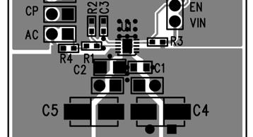
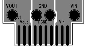
16 YML PCB Layout Recommendations YML Evaluation Board Top Layer YML Evaluation Board Bottom Layer October M B
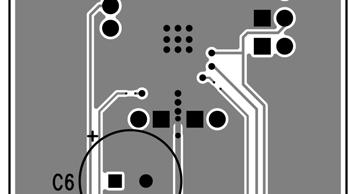
17 YMME Evaluation Board Schematic (1-Pin epad MSOP) Bill of Materials Item Part Number Manufacturer Description Qty. C1 C85ZD16KAT2A AVX (1) 1µF/1V Ceramic Capacitor, X5R,Size 85 1 C3216X5ROJ476M TDK (2) 47µF/6.3V Ceramic Capacitor, X5R, Size 126 or C2 GRM31Cr6J476ME19L Murata (3) 47µF/6.3V Ceramic Capacitor, X5R, Size 126 or D476MAT2A AVX (1) 47µF/6.3V Ceramic Capacitor, X5R, Size 126 C3 C635C14KAT2A AVX (1).1µF/5V Ceramic Capacitor, X7R, Size 63 GRM188R71H14KA93D Murata (3).1µF/5V Ceramic Capacitor, X7R, Size 63 1 R1 CRCW8569R8F Vishay (5) 69.8Ω Film Resistor, Size 85, 1% 1 R2 CRCW8549R9F Vishay (5) 49.9Ω Film Resistor, Size 85, 1% 1 R3 CRCW8512F Vishay (5) 1kΩ Film Resistor, Size 85, 1% 1 R4 CRCW85RF Vishay (5) Ω Film Resistor, Size 85, 1% 1 U1 YMME Micrel, Inc. (6) 3A Low-Voltage, Single-Supply LDO 1 Notes: 1. AVX: 2. TDK: 3. Murata: 4. Vishay: 5. Micrel, Inc.: October M B


18 YMME PCB Layout Recommendations YMME Evaluation Board Top Layer YMME Evaluation Board Bottom Layer October M B
19 Package Information 1-Pin 3mm x 3mm MLF (ML) October M B
20 Package Information (Continued) 1-Pin e-pad MSOP (MME) October M B
21 Landing Pattern 1-Pin 3mm x 3mm MLF (ML) October M B
22 Landing Pattern (Continued) 1-Pin e-pad MSOP (ME) MICREL, INC. 218 FORTUNE DRIVE SAN JOSE, CA USA TEL +1 (48) FAX +1 (48) WEB Micrel makes no representations or warranties with respect to the accuracy or completeness of the information furnished in this data sheet. This information is not intended as a warranty and Micrel does not assume responsibility for its use. Micrel reserves the right to change circuitry, specifications and descriptions at any time without notice. No license, whether express, implied, arising by estoppel or otherwise, to any intellectual property rights is granted by this document. Except as provided in Micrel s terms and conditions of sale for such products, Micrel assumes no liability whatsoever, and Micrel disclaims any express or implied warranty relating to the sale and/or use of Micrel products including liability or warranties relating to fitness for a particular purpose, merchantability, or infringement of any patent, copyright or other intellectual property right. Micrel Products are not designed or authorized for use as components in life support appliances, devices or systems where malfunction of a product can reasonably be expected to result in personal injury. Life support devices or systems are devices or systems that (a) are intended for surgical implant into the body or (b) support or sustain life, and whose failure to perform can be reasonably expected to result in a significant injury to the user. A Purchaser s use or sale of Micrel Products for use in life support appliances, devices or systems is a Purchaser s own risk and Purchaser agrees to fully indemnify Micrel for any damages resulting from such use or sale. 21 Micrel, Incorporated. October M B
MIC2033. General Description. Features. Applications. Typical Application. High-Accuracy, High-Side, Fixed Current Limit Power Switch
 High-Accuracy, High-Side, Fixed Current Limit Power Switch General Description The is a high-side MOSFET power distribution switch providing increased system reliability utilizing 5% current limit accuracy.
Features. Applications
 Dual 500mA µcap Low Dropout, Micropower Linear Regulator General Description The is an advanced dual, micropower, low dropout linear regulator. The provides low quiescent current operation, using only
MIC5396/7/8/9. General Description. Features. Applications. Typical Application. Low-Power Dual 300mA LDO in 1.2mm x 1.
 Low-Power Dual 300mA LDO in 1.2mm x 1.6mm Extra Thin DFN General Description The is an advanced dual LDO ideal for powering general purpose portable devices. The provides two high-performance, independent
MIC5365/6. General Description. Features. Applications. Typical Application. High-Performance Single 150mA LDO
 High-Performance Single 150mA LDO General Description The is an advanced general purpose linear regulator offering high power supply rejection (PSRR) in an ultra-small 1mm 1mm package. The MIC5366 includes
MIC37110/MIC37112 MIC37120/MIC37122
 High-Performance, Low-Noise, 1A LDOs General Description The and are high-performance, low-noise, low dropout regulators. Each of these LDOs is capable of sourcing 1A output current, offers high power
Features. Applications
 High PSRR Low Noise 300mA µcap Ultra-Low Dropout LDO Regulator General Description The is a high-performance, 300mA LDO regulator, offering extremely high PSRR and very low noise while consuming low ground
Features. Applications. RF Power Supply Circuit
 High Performance, Low Noise Dual 500mA ULDO General Description The is a tiny Dual Ultra Low Dropout (ULDO ) linear regulator ideally suited for portable electronics due to its low output noise. The provides
MIC5317. Features. General Description. Applications. Typical Application. High-Performance Single 150mA LDO
 High-Performance Single 150mA LDO General Description The is a high performance 150mA low dropout regulator offering high power supply rejection (PSRR) in an ultra-small 1mm 1mm package for stringent space
MIC5332. Features. General Description. Applications. Typical Application. Micro-Power, High-Performance Dual 300mA ULDO
 Micro-Power, High-Performance Dual 300mA ULDO General Description The is a tiny, dual, low quiescent current LDO ideal for applications that are power sensitive. The integrates two high-performance 300mA
MIC General Description. Features. Applications: Typical Application. 1A High Speed Low VIN LDO
 1A High Speed Low VIN LDO General Description The is a high speed, Low V IN LDO capable of delivering up to 1A and designed to take advantage of point of load applications that use multiple supply rails
MIC5524. Features. General Description. Applications. Typical Application. High-Performance 500mA LDO in Thin DFN Package
 High-Performance 500mA LDO in Thin DFN Package General Description The is a low-power, µcap, low dropout regulator designed for optimal performance in a very-small footprint. It is capable of sourcing
MIC5375/6/7/8. General Description. Features. Applications. Typical Application. High Performance Low Dropout 150mA LDO
 High Performance Low Dropout 150mA LDO General Description The is an advanced general purpose linear regulator offering low dropout in an ultra small package. The MIC5375/6 provides fixed output voltage
Features. Applications
 MIC9431 2mA LDO with Ripple Blocker Technology General Description The MIC9431 Ripple Blocker is a monolithic integrated circuit that provides low-frequency ripple attenuation (switching noise rejection)
MIC5370/1. Features. General Description. Applications. Typical Application. High-Performance Dual 150mA LDO 1.6mm x 1.
 High-Performance Dual 15mA LDO 1.6mm x 1.6mm General Description The is an advanced dual LDO ideal for powering general purpose portable devices. The provides two independently-controlled, highperformance
MIC4812. Features. General Description. Applications. Typical Application
 High Current 6 Channel Linear WLED Driver with DAM and Ultra Fast PWM Control General Description The is a high efficiency linear White LED (WLED) driver designed to drive up to six high current WLEDs
MIC69101/103. General Description. Features. Applications. Typical Application. Single Supply V IN, LOW V IN, LOW V OUT, 1A LDO
 MIC6911/13 Single Supply V IN, LOW V IN, LOW V OUT, 1A LDO General Description The MIC6911/13 is the 1A output current member of the MIC69xxx family of high current, low voltage regulators, which support
Features. Applications. Figure 1. Typical Application Circuit
 3A, Low Voltage, Adjustable LDO Regulator with Dual Input Supply General Description The is a high-bandwidth, low-dropout, 3A voltage regulator ideal for powering core voltages of lowpower microprocessors.
Features. Applications. Adjustable Regulator Application. (*See Minimum Load Current Section)
") 3A, Low Voltage µcap LDO Regulator General Description The is a 3A low-dropout linear voltage regulator that provides a low voltage, high current output with a minimum of external components. It offers
3A, Low Voltage µcap LDO Regulator General Description The is a 3A low-dropout linear voltage regulator that provides a low voltage, high current output with a minimum of external components. It offers
MIC69151/153. General Description. Features. Applications. Typical Application. Single Supply V IN, Low V IN, Low V OUT, 1.5A LDO
 Single Supply V IN, Low V IN, Low V OUT, 1.5A LDO General Description The is the 1.5A output current member of the MIC69xxx family of high current, low voltage regulators, which support currents of 1A,
MIC5501/2/3/4. General Description. Features. Applications. Typical Application. Single 300mA LDO in 1.0mm 1.0mm DFN Package
 Single 300mA LDO in 1.0mm 1.0mm DFN Package General Description The is an advanced general-purpose LDO ideal for powering general-purpose portable devices. The family of products provides a highperformance
MIC General Description. Features. Applications. Typical Application. 3A Low Voltage LDO Regulator with Dual Input Voltages
 3A Low Voltage LDO Regulator with Dual Input Voltages General Description The is a high-bandwidth, low-dropout, 3.0A voltage regulator ideal for powering core voltages of lowpower microprocessors. The
MIC5374/84. Features. General Description. Applications. Typical Application. Triple 200mA µcap LDO and 1mA RTC LDO in 2.5mm x 2.
 Triple 2mA µcap LDO and 1mA RTC LDO in 2.5mm x 2.5mm Thin MLF General Description The is a four output device with three 2mA LDOs and a real time clock (RTC) 1mA LDO which is ideal for application processor
MIC5373/83. Features. General Description. Applications. Typical Application. Triple 200mA µcap LDO in 2.5mm x 2.5mm Thin MLF
 Triple 2mA µcap LDO in 2.5mm x 2.5mm Thin MLF General Description The is a triple output device with three 2mA LDOs which is ideal for application processor support in mobile platforms. The MIC5373 provides
Features. Applications. Portable Application
 500mA LDO in 1.6mm 1.6mm Package General Description The is a high-performance, single-output, ultralow LDO (ULDO ) regulator, offering a low total output noise of 30μV RMS. The is capable of sourcing
Features. MIC5318-x.xYMT EN BYP GND. Portable Application
 High Performance 3mA µcap ULDO General Description The is a high performance, single output ultra low drop-out (ULDO ) regulator, offering low total output noise in an ultra-small Thin MLF package. The
MIC5388/9. Features. General Description. Applications. Typical Application. Dual 200mA Peak LDO in Wafer Level Chip Scale Package
 Dual 2mA Peak LDO in Wafer Level Chip Scale Package General Description The is an advanced dual LDO ideal for powering general purpose portable devices. The provides two independently-controlled, highperformance,
MIC5331. General Description. Features. Applications. Typical Application. Micro-Power High Performance Dual 300mA ULDO
 Micro-Power High Performance Dual 300mA ULDO General Description The is a tiny dual low quiescent current LDO ideal for applications that are power sensitive. The integrates two high performance, 300mA
MIC5387. Features. General Description. Applications. Typical Application. Ultra-Small Triple 150mA Output LDO
 Ultra-Small Triple Output LDO General Description The is an advanced, general-purpose, triple linear regulator offering high power supply rejection (PSRR) in an ultra-small, 6-pin, 1.6mm x 1.6mm Thin MLF
MIC5385. Features. General Description. Applications. Typical Application. Ultra Small Triple 150mA Output LDO
 Ultra Small Triple 1 Output LDO General Description The is an advanced general purpose triple linear regulator offering high power supply rejection (PSRR) in an ultra-small 2mm x 2mm 8 pin Thin MLF package.
MIC4414/4415. General Description. Features. Applications. Typical Application. 1.5A, 4.5V to 18V, Low-Side MOSFET Driver
 MIC4414/4415 1.5A, 4.5V to 18V, Low-Side MOSFET Driver General Description The MIC4414 and MIC4415 are low-side MOSFET drivers designed to switch an N-channel enhancement type MOSFET in low-side switch
MIC5309. Features. General Description. Applications. Typical Application. Low V IN /V OUT 300mA High PSRR ULDO with Ultra-Low IQ
 Low V IN /V OUT 3mA High PSRR ULDO with Ultra-Low IQ General Description The is a high performance, µcap low dropout regulator, offering ultra-low operating current while maintaining very fast transient
MIC5333. General Description. Features. Applications. Typical Application. Micro-Power High Performance Dual 300mA ULDO with Dual POR
 Micro-Power High Performance Dual 300mA ULDO with Dual POR General Description The is a tiny dual low quiescent current LDO ideal for applications that are power sensitive. The integrates two high performance,
MIC5271. Applications. Low. output current). Zero-current off mode. and reduce power. GaAsFET bias Portable cameras. le enable pin, allowing the user
. Zero-current off mode. and reduce power. GaAsFET bias Portable cameras. le enable pin, allowing the user") µcap Negative Low-Dropout Regulator General Description The is a µcap 100mA negativee regulator in a SOT-23-this regulator provides a very accurate supply voltage for applications that require a negative
µcap Negative Low-Dropout Regulator General Description The is a µcap 100mA negativee regulator in a SOT-23-this regulator provides a very accurate supply voltage for applications that require a negative
Features. Applications
 MIC532 15mA ULDO in Ultra-Small 1.2mm x 1.6mm Thin MLF General Description The MIC532 is an ultra-small, ultra-low dropout CMOS regulator, ULDO that is ideal for today s most demanding portable applications
MIC5316. General Description. Features. Applications. Typical Application. Low Voltage Dual 300mA LDO with Power on Reset and Voltage Select
 Low Voltage Dual 300mA LDO with Power on Reset and Voltage Select General Description The is a high performance, dual low input voltage, low dropout regulator with Power On Reset (POR) and voltage select.
MIC General Description. Features. Applications. Typical Application. 5A, Low V IN, Low V OUT µcap LDO Regulator
 MIC6952, Low V IN, Low V OUT µcap LDO Regulator General Description The MIC6952 is a, low dropout linear regulator that provides low voltage high current outputs with a minimum of external components.
MIC5380/1. General Description. Features. Applications. Typical Application. High Performance Dual 150mA LDO 1mm x 1mm Thin MLF
 High Performance Dual 15mA LDO 1mm x 1mm Thin MLF General Description The is an advanced dual LDO ideal for powering space constrained portable devices. The provides two independently controlled, high
MIC General Description. Features. Applications. Typical Application. HELDO 1.5A High Efficiency Low Dropout Regulator
 HELDO 1.5A High Efficiency Low Dropout Regulator General Description The is a 1.5A continuous output current step down converter. This is a follow on product in the new HELDO (High Efficiency Low DropOut
MIC2245. Features. General Description. Applications. Typical Application. 4MHz PWM Synchronous Buck Regulator with LDO Standby Mode
 4MHz PWM Synchronous Buck Regulator with LDO Standby Mode General Description The Micrel is a high efficiency 4MHz pulse width modulated (PWM) synchronous buck (stepdown) regulator that features a LOWQ
Features. MIC5301-x.xYMT EN BYP GND. Portable Application
 Single, 1mA µcap ULDO General Description The is a high performance, single output ultra low LDO (ULDO ) regulator, offering low total output noise. The is capable of sourcing 1mA output current and offers
Features. Applications
 3.0A, Low-Voltage µcap LDO Regulator General Description The Micrel is a 3.0A low-dropout linear voltage regulator that provides a low voltage, high current output with a minimum number of external components.
Features. Applications
 MIC9431 2mA LDO with Ripple Blocker Technology General Description The MIC9431 Ripple Blocker is a monolithic integrated circuit that provides low-frequency ripple attenuation (switching noise rejection)
Features. Applications. V OUT
 MIC535 5mA µcap Ultra-Low Dropout LDO Regulator General Description The MIC535 is a high-performance, 5mA LDO regulator, offering extremely high PSRR and very low noise while consuming low ground current.
Features. RF Power Supply Circuit
 Dual 300mA µcap LDO in 2mm x 2mm MLF General Description The is a tiny Dual Ultra Low Dropout (ULDO ) linear regulator ideally suited for portable electronics due to its high power supply ripple rejection
MIC2251. General Description. Features. Applications. Typical Application. High-Efficiency Low EMI Boost Regulator
 High-Efficiency Low EMI Boost Regulator General Description The is a general purpose DC/DC boost switching regulator that features low noise, EMI reduction circuitry, and high efficiency across a wide
Features. Applications
 High-Current Low-Dropout Regulators General Description The is a high current, high accuracy, lowdropout voltage regulators. Using Micrel's proprietary Super βeta PNP process with a PNP pass element, these
Features. Applications V IN ENABLE SHUTDOWN. C IN = 1.0µF
 300mA High PSRR, Low Noise µcap CMOS LDO General Description The is an efficient CMOS voltage regulator optimized for low-noise applications. It offers 1.5% initial accuracy, low dropout voltage (300mV
Features. Applications
 High Input Voltage Low IQ µcap LDO Regulator General Description The is a 100mA highly accurate, low dropout regulator with high input voltage and ultra-low ground current. This combination of high voltage
MIC Features. General Description. Applications. Typical Application. 1.5A, Low-Voltage µcap LDO Regulator
 1.5A, Low-Voltage µcap LDO Regulator General Description The Micrel is a 1.5A low-dropout linear voltage regulator that provides a low-voltage, high-current output with a minimum of external components.
MIC37150/51/52/53. General Description. Features. Applications. Typical Application. 1.5A, Low Voltage µcap LDO Regulator
 1.5A, Low Voltage µcap LDO Regulator General Description The Micrel is a 1.5A low-dropout linear voltage regulator that provides a low voltage, high current output with a minimum of external components.
MIC General Description. Features. Applications. Typical Application. 1.5A Low Voltage LDO Regulator w/dual Input Voltages
 MIC4915 1.5A Low oltage LDO Regulator w/dual Input oltages General Description The MIC4915 is a high-bandwidth, low-dropout, 1.5A voltage regulator ideal for powering core voltages of lowpower microprocessors.
MIC5225. General Description. Features. Applications. Typical Application. Ultra-Low Quiescent Current 150mA µcap Low Dropout Regulator
 Ultra-Low Quiescent Current 15mA µcap Low Dropout Regulator General Description The is a 15mA highly accurate, low dropout regulator with high input voltage and ultra-low ground current. This combination
MIC3385. General Description. Features. Applications. Typical Application. 8MHz Inductorless Buck Regulator with LDO Standby Mode
 8MHz Inductorless Buck Regulator with LDO Standby Mode General Description The Micrel is a high efficiency inductorless buck regulator that features a LOWQ LDO standby mode that draws only 18µA of quiescent
Features. Applications. Camera DSP Power Supply Circuit
 High-Performance Dual 150mA LDO General Description The is a tiny dual low-dropout linear regulator ideally suited for portable electronics. It is ideal for general purpose/digital applications which require
Features. R1 10k. 10nF. R2 3.83k
 High Efficiency 1MHz Synchronous Buck Regulator General Description The Micrel is a high efficiency 1MHz PWM synchronous buck switching regulator. The features low noise constant frequency PWM operation
MIC37501/ General Description. Features. Applications. Typical Applications. 5A, Low Voltage μcap LDO Regulator
 MIC375/375, Low Voltage μcap LDO Regulator General Description The MIC375 and MIC375 are, low dropout linear voltage regulator that provide low voltage, high current outputs with a minimum of external
MIC5238. General Description. Features. Applications. Typical Application. Ultra-Low Quiescent Current, 150mA µcap LDO Regulator
 Ultra-Low Quiescent Current, 150mA µcap LDO Regulator General Description The is an ultra-low voltage output, 150mA LDO regulator. Designed to operate in a single supply or dual supply mode, the consumes
Features. Applications SOT-23-5
 135MHz, Low-Power SOT-23-5 Op Amp General Description The is a high-speed, unity-gain stable operational amplifier. It provides a gain-bandwidth product of 135MHz with a very low, 2.4mA supply current,
MIC5248. Features. General Description. Applications. Typical Application. 150mA µcap CMOS LDO Regulator w/power Good VIN VOUT C OUT GND
 150mA µcap CMOS LDO Regulator w/power Good General Description The is an efficient, general purpose 1.2V CMOS voltage regulator with a power good output function. The offers better than 3%initial accuracy,
Features. Applications
 Teeny Ultra-Low Power Op Amp General Description The is a rail-to-rail output, operational amplifier in Teeny SC70 packaging. The provides 4MHz gain-bandwidth product while consuming an incredibly low
MIC2215. Features. General Description. Applications. Typical Application. Triple High PSRR, Low Noise µcap LDO
 Triple High PSRR, Low Noise µcap LDO General Description The is a high performance, triple LDO voltage regulator, with each regulator capable of providing 250mA continuous output current. Ideal for battery
MIC General Description. Features. Applications. Dual 2A LDO Regulator
 Dual 2A LDO Regulator General Description The is a dual high peak current LDO regulator designed specifically for powering applications such as FPGA core voltages that require high start up current with
Features. Applications SOT-23-5 (M5)
") 1.8V to 11V, 15µA, 25kHz GBW, Rail-to-Rail Input and Output Operational Amplifier General Description The is a low-power operational amplifier with railto-rail inputs and outputs. The device operates from
1.8V to 11V, 15µA, 25kHz GBW, Rail-to-Rail Input and Output Operational Amplifier General Description The is a low-power operational amplifier with railto-rail inputs and outputs. The device operates from
MIC5310. General Description. Features. Applications. Typical Application. Dual 150mA µcap LDO in 2mm x 2mm MLF
 Dual 15mA µcap LDO in 2mm x 2mm MLF General Description The is a tiny Dual Ultra Low Dropout (ULDO ) linear regulator ideally suited for portable electronics due to its high power supply ripple rejection
MIC A Sequencing LDO with Tracking and Ramp Control. General Description. Features. Applications
 2A Sequencing LDO with Tracking and Ramp Control General Description The is a high peak current LDO regulator designed specifically for powering applications such as FPGA core voltages that require high
MIC5235. General Description. Features. Applications. Typical Application. Ultra-Low Quiescent Current, 150mA µcap LDO Regulator
 MIC535 Ultra-Low Quiescent Current, 5mA µcap LDO Regulator General Description The MIC535 is a 5mA highly accurate, low dropout regulator with high input voltage and ultra-low ground current. This combination
Features. Applications V IN C IN
 3.A, Low-Voltage µcap LDO Regulator General Description The Micrel is a 3.A low-dropout linear voltage regulator that provides a low-voltage, high-current output with a minimum number of external components.
Features. Applications
 Teeny Ultra-Low-Power Op Amp General Description The is a rail-to-rail output, input common-mode to ground, operational amplifier in Teeny SC70 packaging. The provides a 400kHz gain-bandwidth product while
MIC2290. General Description. Features. Applications. Typical Application. 2mm 2mm PWM Boost Regulator with Internal Schotty Diode
 2mm 2mm PWM Boost Regulator with Internal Schotty Diode General Description The is a 1.2MHz, PWM, boost-switching regulator housed in the small size 2mm 2mm 8-pin MLF package. The features an internal
Features. Applications
 MIC9431 2mA LDO with Ripple Blocker Technology General Description The MIC9431 Ripple Blocker is a monolithic integrated circuit that provides low-frequency ripple attenuation (switching noise rejection)
Features. MIC5253-x.xBC5 V IN. Ultra-Low-Noise Regulator Application
 1mA Low Noise µcap Teeny LDO General Description The is an efficient, CMOS voltage regulator optimized for ultra-low-noise applications. It offers 1.5% initial accuracy, extremely low dropout voltage (165mV
MIC2238. General Description. Features. Applications. Typical Application. 2.5MHz Dual Phase PWM Buck Regulator
 2.5MHz Dual Phase PWM Buck Regulator General Description The Micrel is dual output 2-phase synchronous buck (step down) PWM DC/DC switching regulator. Power conversion efficiencies of above 95% are easily
MIC4478/4479/4480. General Description. Features. Applications. Typical Application. 32V Low-Side Dual MOSFET Drivers
 32V Low-Side Dual MOSFET Drivers General Description The MIC4478, MIC4479, and MIC4480 are low-side dual MOSFET drivers are designed to switch N-channel enhancement type MOSFETs from TTL-compatible control
MIC2296. General Description. Features. Applications. High Power Density 1.2A Boost Regulator
 High Power Density 1.2A Boost Regulator General Description The is a 600kHz, PWM dc/dc boost switching regulator available in a 2mm x 2mm MLF package option. High power density is achieved with the s internal
Features ENABLE SHUTDOWN. Ultra-Low-Noise Regulator Application
 5mA Low Noise µcap CMOS LDO General Description The is an efficient, precise CMOS voltage regulator optimized for ultra-low-noise applications. It offers % initial accuracy, extremely-low dropout voltage
Features SLEW ENA ELA VDD. 332k ELB RSW MIC M COM REL ENB GND. VIN Li Ion 3V to 4.2V 2.2nF 250V. Low Noise Dual EL Driver
 Low Noise Dual 22 V PP Driver With Output Voltage Slew Rate Control General Description The is a low noise dual Electroluminescent () Panel driver used in backlighting applications. The converts a low
MIC94161/2/3/4/5. Features. General Description. Applications. Typical Application. 3A High-Side Load Switch with Reverse Blocking
 3A High-Side Load Switch with Reverse Blocking General Description The is a family of high-side load switches designed to operate from 1.7V to 5.5V input voltage. The load switch pass element is an internal
Features. Applications. RF Transceiver
 15mA µcap Dual LDO Regulator General Description The is a dual 15mA LDO in tiny 2.5mm x 2.5mm MLF packaging ideal for applications where cost is the priority. The is ideal for any application in portable
Features. Applications
 3A High-Speed Low V IN DDR Terminator General Description The is a 3A, high-speed, linear, low V IN, double data rate (DDR), memory terminator power supply. The part is small and requires small output
MIC33153 Evaluation Board
 4MHz 1.2A PWM Buck Regulator with HyperLight Load and Power Good General Description This board enables the evaluation of the MIC33153, a fully integrated 1.2A, 4MHz switching regulator featuring HyperLight
Features. Applications. 1.2MHz Boost Converter with OVP in Thin SOT-23-6
 1.2MHz PWM Boost Converter with OVP General Description The is a 1.2MHz pulse width modulated (PWM) step-up switching regulator that is optimized for low power, high output voltage applications. With a
MIC Features. General Description. Applications. Typical Application. 4MHz PWM Buck Regulator with HyperLight Load and Voltage Scaling
 4MHz PWM Buck Regulator with HyperLight Load and Voltage Scaling General Description The Micrel is a high efficiency 600mA PWM synchronous buck (step-down) regulator featuring HyperLight Load, a patented
MIC3975. General Description. Features. Applications. Ordering Information. Typical Applications. 750mA µcap Low-Voltage Low-Dropout Regulator
 MIC3975 750mA µcap Low-Voltage Low-Dropout Regulator General Description The MIC3975 is a 750mA low-dropout linear voltage regulators that provide low-voltage, high-current output from an extremely small
MIC2846A. General Description. Features. Applications. High Efficiency 6 Channel Linear WLED Driver with DAM, Digital Control and Dual Low I Q LDOs
 High Efficiency 6 Channel Linear WLED Driver with DAM, Digital Control and Dual Low I Q LDOs General Description The is a high efficiency White LED (WLED) driver featuring two low quiescent current LDOs.
MIC Features. General Description. Applications. Typical Application. 4MHz PWM Buck Regulator with HyperLight Load Switching Scheme
 4MHz PWM Buck Regulator with HyperLight Load Switching Scheme General Description The Micrel is a high-efficiency, 600mA, PWM, synchronous buck (step-down) regulator featuring the HyperLight Load patented
RT A, Low Input Voltage, Ultra-Low Dropout LDO Regulator with Enable. Features. General Description. Applications. Ordering Information
 RT2516 2A, Low Input Voltage, Ultra-Low Dropout LDO Regulator with Enable General Description The RT2516 is a high performance positive voltage regulator designed for use in applications requiring ultra-low
MIC803. Features. General Description. Applications. Typical Application. 3-Pin Microprocessor Supervisor Circuit with Open-Drain Reset Output
 3-Pin Microprocessor Supervisor Circuit with Open-Drain Reset Output General Description The is a single-voltage supervisor with open-drain reset output that provides accurate power supply monitoring and
MIC23156 Evaluation Board
 1.5A, 3MHz Synchronous Buck Regulator with HyperLight Load and I 2 C Control for Dynamic Voltage Scaling General Description The MIC23156 evaluation board allows the customer to evaluate a fully-integrated
Features. MIC2212-xxBML VOUT2 POR CBYP SET GND. MIC2212 Typical Cell Phone Application
 MIC2212 Dual µcap LDO and Power-On Reset General Description The MIC2212 is a dual µcap low dropout regulator with power-on reset circuit. The first regulator is capable of sourcing 15mA, while the second
Features. Applications
 Comparator with 1.25% Reference and Adjustable Hysteresis General Description The MIC841 and MIC842 are micropower, precision voltage comparators with an on-chip voltage reference. Both devices are intended
RTQ2516-QT. 2A, Low Input Voltage, Ultra-Low Dropout LDO Regulator with Enable. General Description. Features. Applications. Ordering Information
 RTQ2516-QT 2A, Low Input Voltage, Ultra-Low Dropout LDO Regulator with Enable General Description The RTQ2516 is a high performance positive voltage regulator designed for use in applications requiring
MIC MHz PWM 2A Buck Regulator with HyperLight Load and Power Good. General Description. Features. Applications. Typical Application
 3MHz PWM 2A Buck Regulator with HyperLight Load and Power Good General Description The is a high-efficiency 3MHz 2A synchronous buck regulator with HyperLight Load mode, power good output indicator, and
MP2009 Ultra-Low-Noise Low-Dropout, 120mA Linear Regulator
 MP2009 Ultra-Low-Noise Low-Dropout, 120mA Linear Regulator DESCRIPTION The MP2009 is an ultra low noise, low dropout linear regulator. The output voltage of MP2009 ranges from 1.5V to 4.5V in 100mV increments
RT2517A. 1A, 6V, Ultra Low Dropout Linear Regulator. General Description. Features. Applications. Ordering Information. Marking Information
 RT2517A 1A, 6V, Ultra Low Dropout Linear Regulator General Description The RT2517A is a high performance positive voltage regulator designed for applications requiring low input voltage and ultra low dropout
Features. Applications
 105MHz Low-Power SOT23-5 Op Amp General Description The is a high-speed operational amplifier which is unity gain stable regardless of resistive and capacitive load. It provides a gain-bandwidth product
MIC2601/2. Features. General Description. Applications. Typical Application. 1.2A, 1.2MHz/2MHz Wide Input Range Integrated Switch Boost Regulator
 1.2A, 1.2MHz/2MHz Wide Input Range Integrated Switch Boost Regulator General Description The is a 1.2MHz/2MHz, PWM DC/DC boost switching regulator available in a 2mm x 2mm MLF package. High power density
MIC2605/6. Features. General Description. Applications. Typical Application
 0.5A,.2MHz / 2MHz Wide Input Range Boost Regulator with Integrated Switch and Schottky Diode General Description The is a.2mhz/2mhz, PWM DC/DC boost switching regulator available in a 2mm x 2mm MLF package.
MIC5206. General Description. Features. Applications. Typical Application. 150mA Low-Noise LDO Regulator
 MIC526 5mA Low-Noise LDO Regulator General Description The MIC526 is an efficient linear voltage regulator with very low dropout voltage (typically 7 at light loads and 65 at 5mA), and very low ground
RT μA I Q, 250mA Low-Dropout Linear Regulator. General Description. Features
 RT9073 1μA I Q, 250mA Low-Dropout Linear Regulator General Description The RT9073 is a low-dropout (LDO) voltage regulators with enable function that operates from 1.2V to 5.5V. It provides up to 250mA
MIC4223/MIC4224/MIC4225
 Dual 4A, 4.5V to 18V, 15ns Switch Time, Low-Side MOSFET Drivers with Enable General Description The are a family of a dual 4A, High-Speed, Low-side MOSFET drivers with logic-level driver enables. The devices