MIC2846A. General Description. Features. Applications. High Efficiency 6 Channel Linear WLED Driver with DAM, Digital Control and Dual Low I Q LDOs
|
|
|
- Arthur Butler
- 5 years ago
- Views:
Transcription
1 High Efficiency 6 Channel Linear WLED Driver with DAM, Digital Control and Dual Low I Q LDOs General Description The is a high efficiency White LED (WLED) driver featuring two low quiescent current LDOs. It is designed to drive up to six LEDs and greatly extend battery life for portable display backlighting and keypad backlighting in mobile devices. The architecture provides the highest possible efficiency by eliminating switching losses present in traditional charge pumps or inductive boost circuits. With a typical dropout of 40mV at 20mA, the allows the LEDs to be driven directly from the battery eliminating switching noise and losses present with the use of boost circuitry. The features Dynamic Averaged Matching (DAM ) which is specifically designed to get the optimum matching despite process variations. This ensures a typical matching of ±1.5% between all six LED channels. The LED brightness is preset by an external resistor and can be dimmed using a single-wire digital control. The digital interface takes commands from digital programming pulses to change the brightness in a logarithmic scale similar to the eye s perception of brightness. The singlewire digital brightness control is divided into two modes of operation; full brightness mode or battery saving mode for a total of 49 brightness steps. The also features two independently enabled low quiescent current LDOs. Each LDO offers ±3% accuracy over temperature, low dropout voltage 150mA), and low ground current under all load conditions (typically 35µA). Both LDOs can be turned off to draw virtually no current. The is available in the 2.5mm x 2.5mm 14-pin Thin MLF leadless package with a junction temperature range of -40 C to +125 C Datasheet and support documentation can be found on Micrel s web site at: Features WLED Driver High Efficiency (no Voltage Boost losses) Dynamic Average Matching (DAM ) Single wire digital control Input voltage range: 3.0V to 5.5V Dropout of 40mV at 20mA Matching better than ±1.5% (typical) Current accuracy better than ±1.5% (typical) Maintains proper regulation regardless of how many channels are utilized LDOs Very low ground current Typical 35µA Stable with 1µF ceramic output capacitor Dropout at 150mV at 150mA Thermal shutdown and current limit protection Available in a 2.5mm x 2.5mm 14-pin Thin MLF package Applications Mobile handsets LCD Handset backlighting Handset keypad backlighting Digital cameras Portable media/mp3 players Portable navigation devices (GPS) Portable applications DAM, Dynamic Average Matching is a trademark of Micrel, Inc. MLF and MicroLeadFrame are registered trademark Amkor Technology Inc. Micrel Inc Fortune Drive San Jose, CA USA tel +1 (408) fax + 1 (408) April 2010 M D
2 Typical Application Digital LCD Display Backlight with 6 WLEDs and Camera Module 6 Digital High Current Flash Driver April M D
3 Ordering Information (1,2,3) Part Number Mark Code LDO1 VOUT LDO2 VOUT Temperature Range Package -MFYMT YPMF 2.8V 1.5V 40 C to +125 C 14-Pin 2.5mm x 2.5mm TMLF -MGYMT YPMG 2.8V 1.8V 40 C to +125 C 14-Pin 2.5mm x 2.5mm TMLF -PGYMT YPPG 3.0V 1.8V 40 C to +125 C 14-Pin 2.5mm x 2.5mm TMLF -PPYMT YPPP 3.0V 3.0V 40 C to +125 C 14-Pin 2.5mm x 2.5mm TMLF -SCYMT YPSC 3.3V 1.0V 40 C to +125 C 14-Pin 2.5mm x 2.5mm TMLF Note: 1. Thin MLF = Pin 1 identifier. 2. Thin MLF is a GREEN RoHS-compliant package. Lead finish is NiPdAu. Mold compound is halogen free. 3. Contact Micrel for other output voltages. Pin Configuration Pin Description 14-Pin 2.5mm x 2.5mm Thin MLF (MT) (Top View) Pin Number Pin Name Pin Function 1 VIN Voltage Input. Connect at least 1µF ceramic capacitor between VIN and GND. 2 LDO2 Output of LDO2. Connect at least 1µF ceramic output capacitor. 3 EN2 Enable Input for LDO2. Active High Input. Logic High = On; Logic Low = Off; Do not leave floating. 4 DC Enable input for LED driver. Can be used for dimming using the digital control interface. See Digital Dimming Interface for details. Do not leave floating. 5 RSET An internal 1.27V reference sets the nominal maximum LED current. Example, apply a 20.5kΩ resistor between RSET and GND to set LED current to 20mA at 100% duty cycle. 6 D1 LED1 driver. Connect LED anode to VIN and cathode to this pin. 7 D2 LED2 driver. Connect LED anode to VIN and cathode to this pin. 8 D3 LED3 driver. Connect LED anode to VIN and cathode to this pin. 9 GND Ground. 10 D4 LED4 driver. Connect LED anode to VIN and cathode to this pin. 11 D5 LED5 driver. Connect LED anode to VIN and cathode to this pin. 12 D6 LED6 driver. Connect LED anode to VIN and cathode to this pin. 13 EN1 Enable Input for LDO1. Active High Input. Logic High = On; Logic Low = Off; Do not leave floating. 14 LDO1 Output of LDO1. Connect at least 1µF ceramic output capacitor. EPAD HS PAD Heat sink pad. Not internally connected. Connect to ground. April M D
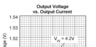
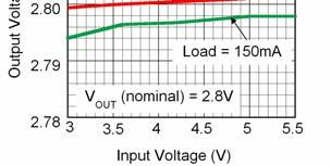
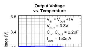
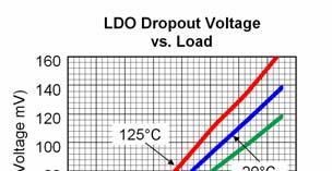
4 Absolute Maximum Ratings (1) Main Input Voltage (V IN ) V to +6V Enable Input Voltage (V DC, V EN1, V EN2 ) V to +6V LED Driver Voltage (V D1-D6 ) V to +6V Power Dissipation... Internally Limited (3) Lead Temperature (soldering, 10sec.) C Storage Temperature (T s ) C to +150 C ESD Rating (4)... ESD Sensitive Operating Ratings (2) Supply Voltage (V IN ) V to +5.5V Enable Input Voltage (V DC, V EN1, V EN2 )... 0V to V IN LED Driver Voltage (V D1-6 )... 0V to V IN Junction Temperature (T J ) C to +125 C Junction Thermal Resistance 2.5mm x 2.5mm Thin MLF-14L (θ JA )...89 C/W Electrical Characteristics Linear WLED Drivers V IN = V DC = 3.8V, V EN1 = V EN2 = 0V, R SET = 20.5kΩ; V D1-D6 = 0.6V; T J = 25 C, bold values indicate 40 C T J 125 C; unless noted. Parameter Conditions Min Typ Max Units Current Accuracy (5) 1.5 % Matching (6) 1.5 % Drop-out Where I LED = 90% of LED current seen at V DROPNOM = 0.6V, 100% brightness level mv Ground/Supply Bias Current I LED = 20mA ma Shutdown Current (current source leakage) Digital Dimming V DC Input Voltage (V DC ) V DC = 0V for more than 1260µs µa Logic Low 0.2 V Logic High 1.2 V V DC Enable Input Current V DC = 1.2V µa t SHUTDOWN Time DC pin is low to shutdown the device 1260 µs t MODE_UP Time DC pin is low to change to Count Up Mode µs t MODE_DOWN Time DC pin is low to change to Count Down Mode µs t PROG_HIGH, t PROG_LOW Time for valid edge count; Ignored if outside limit range 2 32 µs t DELAY t PROG_SETUP t START_UP Time DC pin must remain high before a mode change can occur First down edge must occur in this window during presetting brightness Delay time starting when DC is first pulled high until LEDs start up 100 µs 5 75 µs 140 µs LDOs V IN = V EN1 = V EN2 = 3.8V, V DC = 0V; C OUT1 = C OUT2 = 1μF, I OUT1 = I OUT1 = 100μA; T J = 25 C, bold values indicate 40 C T J 125 C; unless noted. Parameter Conditions Min Typ Max Units Output Voltage Accuracy Variation from nominal V OUT V IN Line Regulation %/V Load Regulation I OUT = 100μA to 150mA 7 mv Dropout Voltage (7) V OUT >= 3.0V; I OUT = 150mA mv Ground Pin Current µa Ground Pin Current in Shutdown V EN = 0V µa % % April M D
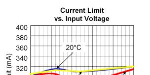
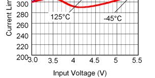
5 LDOs (continued) Parameter Conditions Min Typ Max Units Ripple Rejection f = 1kHz; C OUT = 2.2μF 65 db Current Limit V OUT = 0V ma Output Voltage Noise Frequency 10Hz to 100kHz 200 µv RMS Enable Inputs (EN1,2) Enable Input Voltage Logic Low 0.2 V Logic High 1.2 V Enable Input Current V EN1 = V EN1 = 1.2V µa Turn-on Time C OUT = 1µF; 90% of V OUT µs Notes: 1. Exceeding the absolute maximum rating may damage the device. 2. The device is not guaranteed to function outside its operating rating. 3. The maximum allowable power dissipation of any T A (ambient temperature) is P D(max) = (T J(max) T A ) / θ JA. Exceeding the maximum allowable power dissipation will result in excessive die temperature, and the regulator will go into thermal shutdown (150 C). 4. Devices are ESD sensitive. Handling precautions recommended. Human Body Model (HBM), 1.5kΩ in series with 100pF. 5. As determined by average current of all channels in use and all channels loaded. 6. The current through each channel meets the stated limits from the average current of all channels. 7. Dropout voltage is defined as the input-output differential at which the output voltage drops 2% below its nominal value measured at V IN = V OUT + 1V. April M D
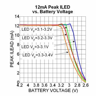
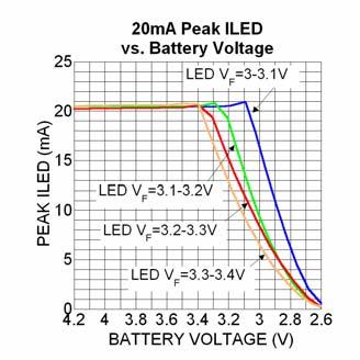
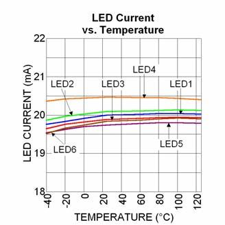
6 Typical Characteristics (WLED Driver) April M D
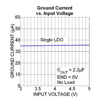
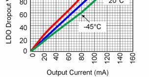
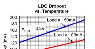
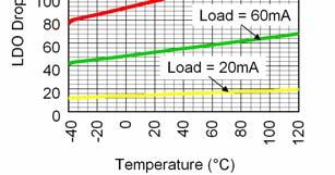
7 Typical Characteristics (LDO) April M D
8 Functional Characteristics (WLED Driver) April M D
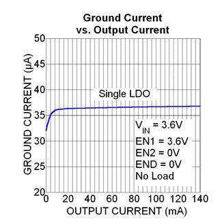
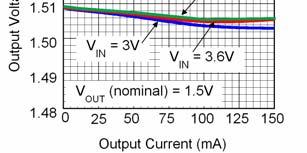
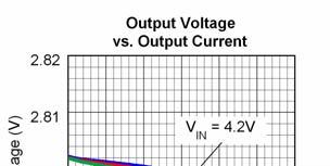
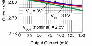
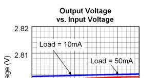
9 Functional Characteristics (LDO) April M D
10 Functional Diagram Figure 1. Functional Block Diagram Functional Description The is a six channel linear LED driver with dual 150mA LDOs. The LED driver incorporates a Dynamic Averaged Matching TM (DAM TM ) technique designed specifically to optimize on current accuracy and matching across process variation. It can maintain proper current regulation with LED current accuracy of 1.5% while the typical matching between the six channels is 1.5% at room temperature. The LED currents are independently driven from the input supply and will maintain regulation with a dropout of 40mV at 20mA. The low dropout of the linear LED Drivers allows the LEDs to be driven directly from the battery voltage and eliminates the need for boost or large and inefficient charge pumps. The maximum LED current for each channel is set via an external resistor while a single-wire digital interface controls dimming. The has two LDOs with a dropout voltage of 150mV at 150mA and consume 35µA of current in operation. Each LDO has an independent enable pin, which reduces the operating current to less than 1µA in shutdown. Both linear regulators are stable with just 1µF of output capacitance. Block Diagram As shown in Figure 1, the consists of two LDOs with six current mirrors set to copy a master current determined by R SET. The linear LED drivers have a designated control block for enabling and dimming of the LEDs. The dimming is controlled by the Digital Control block that receives digital signals for dimming. The LDOs each have their own control and are independent of the linear LED drivers. Each LDO consists of internal feedback resistors, an error amplifier, a PFET transistor and a control circuit for enabling. April M D
 pin and the ground (GND) pin. Refer to the layout recommendations section for details on placing the input capacitor (C1).")
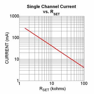
11 VIN The input supply (VIN) provides power to the LDOs, the linear LED drivers and the control circuitry. The V IN operating range is 3V to 5.5V. A minimum bypass capacitor of 1µF should be placed close to the input (VIN) pin and the ground (GND) pin. Refer to the layout recommendations section for details on placing the input capacitor (C1). LDO1/LDO2 The output pins for LDO one and LDO two are labeled LDO1 and LDO2, respectively. A minimum of 1µF bypass capacitor should be placed as close as possible to the output pin of each LDO. Refer to the layout recommendations section for details on placing the output capacitor (C2, C3) of the LDOs. EN1/EN2 A logic high signal on the enable pin activates the LDO output voltage of the device. A logic low signal on the enable pin deactivates the output and reduces supply current to less than 1µA. EN1 controls LDO1 and EN2 controls LDO2. Do not leave these control pins floating. DC The DC pin is used to enable and control dimming of the linear drivers on the. See the Digital Dimming Interface in the Application Information section for details. Pulling the DC pin low for more than 1260μs puts the into a low I Q sleep mode. The DC pin cannot be left floating; a floating enable pin may cause an indeterminate state on the outputs. A 200kΩ pull down resistor is recommended. R SET Figure 2. Peak LED Current vs. R SET (100% Duty Cycle) D1-D6 The D1 through D6 pins are the LED driver for LED 1 through 6, respectively. The anodes of the LEDs are connected to VIN and the cathodes of the LEDs are connected to D1 through D6. When operating with less than six LEDs, leave the unused D pins unconnected. The six LED channels are independent of one another and may be combined or used separately. During startup, the D1 through D6 channels are turned on in synchronization at around 250µs apart. GND The ground pin is the ground path for the linear drivers and LDOs. The ground of the input capacitor should be routed with low impedance traces to the GND pin and made as short as possible. Refer to the layout recommendations for more details. The R SET pin is used by connecting a R SET resistor to ground to set the peak current of the linear LED driver. The average LED current can be calculated by the equation (1). I LED (ma) = 410 * ADC / R SET (kω) (1) ADC is the average duty cycle of the LED current controlled by the single-wire digital dimming. See Table 1 for ADC values. When the device is fully on the average duty cycle equals 100% (ADC=1). A plot of I LED versus R SET at 100% duty cycle is shown in Figure 2. April M D
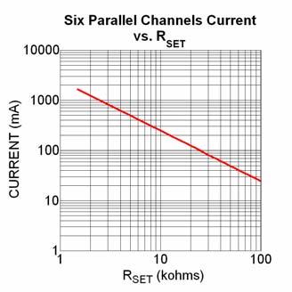
12 Application Information Brightness Level (0-48) Average Duty Cycle (%) Average I LED (ma) I PEAK (ma) 60% of I PEAK R SET = 20.5kΩ I PEAK = 12mA % of I PEAK Table 1. Digital Interface Brightness Level Table 100% of I PEAK R SET = 20.5kΩ I PEAK = 20mA Dynamic Average Matching (DAM ) The Dynamic Average Matching architecture multiplexes four voltage references to provide highly accurate LED current and channel matching. The achieves industry leading LED channel matching of 1.5% across the entire dimming range. High Current Parallel Operation Digital 6 Figure 3. High Current LED Driver Circuit The linear drivers are independent of each other and can be used individually or paralleled in any combination for higher current 4applications. A single WLED can be driven with all 6 linear drivers by connecting D1 through D6 in parallel to the cathode of the WLED as shown in Figure 3. This will generate a current 6 times the individual channel current and can be used for higher current WLEDs such as those used in flash or torch applications. Digital Dimming The utilizes an internal dynamic pulse width to generate an average duty cycle for each brightness level. By varying the duty cycle the average current achieves 49 logarithmically spaced brightness levels. This generates a brightness scale similar to the perception of brightness seen by the human eye. Figure 4 shows the LED current at different brightness levels. When dimming, the D1 through D6 pins are 60 out of phase from each other to reduce electromagnetic interference. The uses an internal frequency of approximately 700Hz to dim the WLEDs. With the period of approximately 1.43ms, the 60 phase shift equates to a timing offset of 238μs. As shown in Figure 5, brightness level 32 was selected to show the phase shift across the channels. April M D
, the will")
13 brightness level. Figure 4. LED Current with Brightness Level Change Start Up Assuming the has been off for a long time and no presetting brightness command is issued (presetting is discussed in a later section), the will start-up in its default mode approximately 140µs (t START_UP ) after a logic level high is applied to the DC pin, shown in Figure 6. In the default mode the LEDs are turned on at the maximum brightness level of 48. Each falling edge during the t PROG_SETUP period will cause the default brightness level to decrease by one. This is discussed in more detail in the Presetting Brightness section. Figure 6. Typical Start-Up Timing Figure 5. LED Current 60 Phase Shift Digital Dimming Interface The incorporates an easy to use single-wire, serial programming interface that allows users to set LED brightness up to 49 different levels, as shown in the table1. Brightness levels 0 through 15 are logarithmically spaced with a peak current equal to 60% of the current programmed by R SET. Brightness level 16 is provided for applications that want to fade to black with no current flowing through the LEDs. Brightness Level 17 has the same duty cycle as level 18, but the peak current is only 60% of the current set by R SET ; therefore, the average current is 0.1mA. Brightness levels 18 through 48 are also logarithmically spaced, but the peak current is equal to 100% of the current determined by R SET. Refer to Table 1 for the translation from brightness level to average LED duty cycle and current. The is designed to receive programming pulses to increase or decrease brightness. Once the brightness change signal is received, the DC pin is simply pulled high to maintain the brightness. This set and forget feature relieves processor computing power by eliminating the need to constantly send a PWM signal to the dimming pin. With a digital control interface, brightness levels can also be preset so that LEDs can be turned on at any particular Shutdown Whenever the DC input pin is pulled low for a period greater than or equal to t SHUTDOWN (1260µs), the will be shutdown as shown in Figure 7. Figure 7. Shutdown Timing Once the device is shutdown, the control circuit supply is disabled and the LEDs are turned off, drawing only 0.01µA. Brightness level information stored in the prior to shutdown will be erased. Count Up Mode/Count Down Mode The mode of can be in either Count Up Mode or Count Down Mode. The Count Down/Up Modes determine what the falling edges of the programming pulses will do to the brightness. In Count Up Mode, subsequent falling edges will increase brightness while in Count Down Mode, subsequent falling edges will decrease brightness. By default, the is in Count Down Mode when first turned on. The counting mode can be changed to Count Up Mode, by pulling the DC pin low for a period equal to t MODE_UP (100µs to 160µs), shown in Figure 8. The device will remain in April M D
14 Count Up Mode until its mode is changed to Count Down Mode or by disabling the to reset the mode back to default. Figure 8. Mode Change to Count Up To change the mode back to Count Down Mode, pull the DC pin low for a period equal to t MODE_DOWN (420µs to 500µs), shown in Figure 9. Now the internal circuitry will remain in Count Down Mode until changed to Count Up as described previously. Figure10. Brightness Programming Pulses Multiple brightness levels can be set as shown in Figure 11. When issuing multiple brightness level adjustments to the DC pin, ensure both t PROG_LOW and t PROG_HIGH are within 2µs to 32µs. To maintain operation at the current brightness level simply maintain a logic level high at the DC pin. Figure 9. Mode Change to Count Down Programming the Brightness Level is designed to start driving the LEDs 140µs (t START_UP ) after the DC pin is first pulled high at the maximum brightness level of 48. After start up, the internal control logic is ready to decrease the LED brightness upon receiving programming pulses (negative edges applied to DC pin). Since starts in Count Down Mode, the brightness level can be decreased without a mode change by applying two programming pulses, as shown in Figure10. Note that the extra pulse is needed to decrease brightness because the first edge is ignored. Anytime the first falling edge occurs later than 32µs after a Mode Change, it will be ignored. Ignoring the first falling edge is necessary in order that Mode Change (t MODE_UP, t MODE_DOWN ) pulses do not result in adjustments to the brightness level. Each programming pulse has a high (t PROG_HIGH ) and a low (t PROG_LOW ) pulse width that must be between 2µs to 32µs. The will remember the brightness level and mode it was changed to. For proper operation, ensure that the DC pin remains high for at least t DELAY (140µs) before issuing a mode change command. Figure11. Decreasing Brightness Several Levels As mentioned, can be programmed to set LED drive current to produce one of 49 distinct brightness levels. The internal logic keeps track of the brightness level with an Up/Down counter circuit. The following section explains how the brightness counter functions with continued programming edges. Counter Roll-Over The internal up/down counter contains registers from 0 to 48 (49 levels). When the brightness level is at 0 and a programming pulse forces the brightness to step down, then the counter will roll-over to level 48. This is illustrated in Figure 12. Figure 12. Down Counter Roll-Over April M D
15 Similarly, when the counter mode is set to Count Up and a programming pulse forces the brightness level to step up from level 48, then the counter will roll-over to level 0 as illustrated in Figure 13. Figure 13. Up Counter Roll-Over Presetting Brightness Presetting the brightness will allow the to start-up at any brightness level (0 to 48). The does not turn on the linear LED driver until the DC pin is kept high for t START_UP (140µs). This grants the user time to preset the brightness level by sending a series of programming edges via the DC pin. The precise timing for the first down edge is between 5µs to 75µs after the DC pin is first pulled high. The 70µs timeframe between 5µs and 75µs is the t PROG_SETUP period. The first presetting pulse edge must occur somewhere between the timeframe of 5µs to 75µs, otherwise the may continue to start up at the full (default) brightness level. One-Step Brightness Changes The One-Step brightness change procedure relieves the user from keeping track of the s up/down counter mode. It combines a Mode Change with a programming edge; therefore, regardless of the previous Count Mode, it will change the brightness level by one. Figure 14. One-Step Brightness Decrease The One-Step Brightness Decrease method is quite simple. First, the DC pin is pulled low for a period equal to the t MODE_DOWN (420µs to 500µs) and immediately followed by a falling edge within t PROG_HIGH (2µs to 32µs) as shown in Figure 14. This will decrease the brightness level by 1. Similarly a One-Step Brightness Increase can be assured by first generating a DC down pulse whose period is equal to the t MODE_UP (100µs to 160µs) and immediately followed by a falling edge within t PROG_HIGH (2µs to 32µs). Figure 15 illustrates the proper timing for execution of a One-Step Brightness Increase. Figure 16. Presetting Timing Figure 16 shows the correct presetting sequence to set the brightness to level 39 prior to start up. Notice that when using the presetting feature the first programming pulse is not ignored. This is because the counter s default mode is Count Down and a Mode Change cannot be performed in the presetting mode. (Note that the t PROG_HIGH and t PROG_LOW pulse width must still be between 2µs to 32µs.) Figure 15. One-Step Brightness Increase April M D
16 LDO LDOs are low noise 150mA LDOs. The LDO regulator is fully protected from damage due to fault conditions, offering linear current limiting and thermal shutdown. Input Capacitor The stability can be maintained using a ceramic input capacitor of 1µF. Low-ESR ceramic capacitors provide optimal performance at a minimum amount of space. Additional high-frequency capacitors, such as small-valued NPO dielectric-type capacitors, help filter out high-frequency noise and are good practice in any noise sensitive circuit. X5R or X7R dielectrics are recommended for the input capacitor. Y5V dielectrics lose most of their capacitance over temperature and are therefore, not recommended. Output Capacitor The LDOs require an output capacitor of at least 1µF or greater to maintain stability, however, the output capacitor can be increased to 2.2µF to reduce output noise without increasing package size. The design is optimized for use with low-esr ceramic chip capacitors. High ESR capacitors are not recommended because they may cause high frequency oscillation. X7R/X5R dielectric-type ceramic capacitors are recommended due to their improved temperature performance compared to Z5U and Y5V capacitors. X7R-type capacitors change capacitance by 15% over their operating temperature range and are the most stable type of ceramic capacitors. Z5U and Y5V dielectric capacitors change value by as much as 50% and 60%, respectively, over their operating temperature ranges. To use a ceramic chip capacitor with Y5V dielectric, the value must be much higher than an X7R ceramic capacitor to ensure the same minimum capacitance over the equivalent operating temperature range. No-Load Stability Unlike many other voltage regulators, the LDOs will remain stable and in regulation with no load. Thermal Considerations The LDOs are each designed to provide 150mA of continuous current. Maximum ambient operating temperature can be calculated based on the output current and the voltage drop across the part. For example if the input voltage is 3.6V, the output voltage is 2.8V, and the output current = 150mA. The actual power dissipation of the regulator circuit can be determined using the equation: P LDO1 = (V IN V OUT1 ) I OUT + V IN I GND Because this device is CMOS and the ground current (I GND ) is typically <100µA over the load range, the power dissipation contributed by the ground current is < 1% and can be ignored for this calculation. P LDO1 = (3.6V 2.8V) 150mA P LDO1 = 0.120W Since there are two LDOs in the same package, the power dissipation must be calculated individually and then summed together to arrive at the total power dissipation. P TOTAL = P LDO1 + P LDO2 To determine the maximum ambient operating temperature of the package, use the junction-to-ambient thermal resistance (θ JA = 60 C/W) of the device and the following basic equation: TJ(max) TA P = TOTAL(max) θ JA T J(max) = 125 C, is the maximum junction temperature of the die and θ JA, is the thermal resistance = 60 C/W. Substituting P TOTAL for P TOTAL(max) and solving for the ambient operating temperature will give the maximum operating conditions for the regulator circuit. For example, when operating the LDOs (LDO1=2.8V and LDO2=1.5V) at an input voltage of 3.6V with 150mA load on each, the maximum ambient operating temperature T A can be determined as follows: P LDO1 = (3.6V 2.8V) 150mA = 0.120W P LDO2 = (3.6V 1.5V) 150mA = 0.315W P TOTAL =0.120W W = 0.435W = (125 C T A )/(60 C/W) T A = 125 C 0.435W 60 C/W T A = 98.9 C Therefore, under the above conditions, the maximum ambient operating temperature of 98.9 C is allowed. April M D
17 Typical Application Circuit 6 Digital Bill of Materials Item Part Number Manufacturer Description Qty. C1608X5R0J105K TDK (1) C1, C2, 06036D105KAT2A AVX (2) C3 GRM188R60J105KE19D Murata (3) Ceramic Capacitor, 1µF, 6.3V, X5R, Size VJ0603G225KXYAT Vishay (4) D1 D6 SWTS1007 Seoul Semiconductor (5) UNC EverLight (6) WLED 6 R1 CRCW060320K5F5EA Vishay (4) Resistor, 20.5k, 1%, 1/16W, Size R2 CRCW FKEA Vishay (4) Resistor, 200k, 1%, 1/16W, Size (7) 6 Channel Digital Control Linear WLED Driver with U1 -xxymt Micrel, Inc. DAM and Dual Low IQ LDO Notes: 1. TDK: 2. AVX: 3. Murata: 4. Vishay: 5. Seoul Semiconductor: 6. EverLight: 7. Micrel, Inc.: 1 April M D


18 PCB Layout Recommendations (Fixed) Top Layer Bottom Layer April M D
19 Package Information 14-Pin (2.5mm x 2.5mm) Thin MLF (MT) MICREL, INC FORTUNE DRIVE SAN JOSE, CA USA TEL +1 (408) FAX +1 (408) WEB The information furnished by Micrel in this data sheet is believed to be accurate and reliable. However, no responsibility is assumed by Micrel for its use. Micrel reserves the right to change circuitry and specifications at any time without notification to the customer. Micrel Products are not designed or authorized for use as components in life support appliances, devices or systems where malfunction of a product can reasonably be expected to result in personal injury. Life support devices or systems are devices or systems that (a) are intended for surgical implant into the body or (b) support or sustain life, and whose failure to perform can be reasonably expected to result in a significant injury to the user. A Purchaser s use or sale of Micrel Products for use in life support appliances, devices or systems is a Purchaser s own risk and Purchaser agrees to fully indemnify Micrel for any damages resulting from such use or sale Micrel, Incorporated. April M D
MIC4812. Features. General Description. Applications. Typical Application
 High Current 6 Channel Linear WLED Driver with DAM and Ultra Fast PWM Control General Description The is a high efficiency linear White LED (WLED) driver designed to drive up to six high current WLEDs
MIC5375/6/7/8. General Description. Features. Applications. Typical Application. High Performance Low Dropout 150mA LDO
 High Performance Low Dropout 150mA LDO General Description The is an advanced general purpose linear regulator offering low dropout in an ultra small package. The MIC5375/6 provides fixed output voltage
MIC5385. Features. General Description. Applications. Typical Application. Ultra Small Triple 150mA Output LDO
 Ultra Small Triple 1 Output LDO General Description The is an advanced general purpose triple linear regulator offering high power supply rejection (PSRR) in an ultra-small 2mm x 2mm 8 pin Thin MLF package.
MIC5387. Features. General Description. Applications. Typical Application. Ultra-Small Triple 150mA Output LDO
 Ultra-Small Triple Output LDO General Description The is an advanced, general-purpose, triple linear regulator offering high power supply rejection (PSRR) in an ultra-small, 6-pin, 1.6mm x 1.6mm Thin MLF
MIC5396/7/8/9. General Description. Features. Applications. Typical Application. Low-Power Dual 300mA LDO in 1.2mm x 1.
 Low-Power Dual 300mA LDO in 1.2mm x 1.6mm Extra Thin DFN General Description The is an advanced dual LDO ideal for powering general purpose portable devices. The provides two high-performance, independent
MIC5316. General Description. Features. Applications. Typical Application. Low Voltage Dual 300mA LDO with Power on Reset and Voltage Select
 Low Voltage Dual 300mA LDO with Power on Reset and Voltage Select General Description The is a high performance, dual low input voltage, low dropout regulator with Power On Reset (POR) and voltage select.
MIC5309. Features. General Description. Applications. Typical Application. Low V IN /V OUT 300mA High PSRR ULDO with Ultra-Low IQ
 Low V IN /V OUT 3mA High PSRR ULDO with Ultra-Low IQ General Description The is a high performance, µcap low dropout regulator, offering ultra-low operating current while maintaining very fast transient
MIC5365/6. General Description. Features. Applications. Typical Application. High-Performance Single 150mA LDO
 High-Performance Single 150mA LDO General Description The is an advanced general purpose linear regulator offering high power supply rejection (PSRR) in an ultra-small 1mm 1mm package. The MIC5366 includes
MIC5524. Features. General Description. Applications. Typical Application. High-Performance 500mA LDO in Thin DFN Package
 High-Performance 500mA LDO in Thin DFN Package General Description The is a low-power, µcap, low dropout regulator designed for optimal performance in a very-small footprint. It is capable of sourcing
MIC5331. General Description. Features. Applications. Typical Application. Micro-Power High Performance Dual 300mA ULDO
 Micro-Power High Performance Dual 300mA ULDO General Description The is a tiny dual low quiescent current LDO ideal for applications that are power sensitive. The integrates two high performance, 300mA
Features. Applications
 MIC532 15mA ULDO in Ultra-Small 1.2mm x 1.6mm Thin MLF General Description The MIC532 is an ultra-small, ultra-low dropout CMOS regulator, ULDO that is ideal for today s most demanding portable applications
MIC5332. Features. General Description. Applications. Typical Application. Micro-Power, High-Performance Dual 300mA ULDO
 Micro-Power, High-Performance Dual 300mA ULDO General Description The is a tiny, dual, low quiescent current LDO ideal for applications that are power sensitive. The integrates two high-performance 300mA
MIC5333. General Description. Features. Applications. Typical Application. Micro-Power High Performance Dual 300mA ULDO with Dual POR
 Micro-Power High Performance Dual 300mA ULDO with Dual POR General Description The is a tiny dual low quiescent current LDO ideal for applications that are power sensitive. The integrates two high performance,
MIC5380/1. General Description. Features. Applications. Typical Application. High Performance Dual 150mA LDO 1mm x 1mm Thin MLF
 High Performance Dual 15mA LDO 1mm x 1mm Thin MLF General Description The is an advanced dual LDO ideal for powering space constrained portable devices. The provides two independently controlled, high
Features. Applications
 High PSRR Low Noise 300mA µcap Ultra-Low Dropout LDO Regulator General Description The is a high-performance, 300mA LDO regulator, offering extremely high PSRR and very low noise while consuming low ground
MIC5370/1. Features. General Description. Applications. Typical Application. High-Performance Dual 150mA LDO 1.6mm x 1.
 High-Performance Dual 15mA LDO 1.6mm x 1.6mm General Description The is an advanced dual LDO ideal for powering general purpose portable devices. The provides two independently-controlled, highperformance
MIC General Description. Features. Applications: Typical Application. 1A High Speed Low VIN LDO
 1A High Speed Low VIN LDO General Description The is a high speed, Low V IN LDO capable of delivering up to 1A and designed to take advantage of point of load applications that use multiple supply rails
MIC5317. Features. General Description. Applications. Typical Application. High-Performance Single 150mA LDO
 High-Performance Single 150mA LDO General Description The is a high performance 150mA low dropout regulator offering high power supply rejection (PSRR) in an ultra-small 1mm 1mm package for stringent space
MIC5501/2/3/4. General Description. Features. Applications. Typical Application. Single 300mA LDO in 1.0mm 1.0mm DFN Package
 Single 300mA LDO in 1.0mm 1.0mm DFN Package General Description The is an advanced general-purpose LDO ideal for powering general-purpose portable devices. The family of products provides a highperformance
Features. Applications. Portable Application
 500mA LDO in 1.6mm 1.6mm Package General Description The is a high-performance, single-output, ultralow LDO (ULDO ) regulator, offering a low total output noise of 30μV RMS. The is capable of sourcing
Features. MIC5301-x.xYMT EN BYP GND. Portable Application
 Single, 1mA µcap ULDO General Description The is a high performance, single output ultra low LDO (ULDO ) regulator, offering low total output noise. The is capable of sourcing 1mA output current and offers
MIC3289. General Description. Features. 1.2MHz PWM White LED Driver with Internal Schottky Diode and True 1-Wire Digital Control.
 1.2MHz PWM White LED Driver with Internal Schottky Diode and True 1-Wire Digital Control General Description The is a PWM boost-switching regulator that is optimized for constant-current white LED driver
Features. Applications
 Dual 500mA µcap Low Dropout, Micropower Linear Regulator General Description The is an advanced dual, micropower, low dropout linear regulator. The provides low quiescent current operation, using only
Features. MIC5318-x.xYMT EN BYP GND. Portable Application
 High Performance 3mA µcap ULDO General Description The is a high performance, single output ultra low drop-out (ULDO ) regulator, offering low total output noise in an ultra-small Thin MLF package. The
MIC5374/84. Features. General Description. Applications. Typical Application. Triple 200mA µcap LDO and 1mA RTC LDO in 2.5mm x 2.
 Triple 2mA µcap LDO and 1mA RTC LDO in 2.5mm x 2.5mm Thin MLF General Description The is a four output device with three 2mA LDOs and a real time clock (RTC) 1mA LDO which is ideal for application processor
MIC5373/83. Features. General Description. Applications. Typical Application. Triple 200mA µcap LDO in 2.5mm x 2.5mm Thin MLF
 Triple 2mA µcap LDO in 2.5mm x 2.5mm Thin MLF General Description The is a triple output device with three 2mA LDOs which is ideal for application processor support in mobile platforms. The MIC5373 provides
Features. Applications. RF Power Supply Circuit
 High Performance, Low Noise Dual 500mA ULDO General Description The is a tiny Dual Ultra Low Dropout (ULDO ) linear regulator ideally suited for portable electronics due to its low output noise. The provides
Features. Applications. Camera DSP Power Supply Circuit
 High-Performance Dual 150mA LDO General Description The is a tiny dual low-dropout linear regulator ideally suited for portable electronics. It is ideal for general purpose/digital applications which require
MIC5238. General Description. Features. Applications. Typical Application. Ultra-Low Quiescent Current, 150mA µcap LDO Regulator
 Ultra-Low Quiescent Current, 150mA µcap LDO Regulator General Description The is an ultra-low voltage output, 150mA LDO regulator. Designed to operate in a single supply or dual supply mode, the consumes
Features. Applications
 MIC9431 2mA LDO with Ripple Blocker Technology General Description The MIC9431 Ripple Blocker is a monolithic integrated circuit that provides low-frequency ripple attenuation (switching noise rejection)
Features. Applications
 High Input Voltage Low IQ µcap LDO Regulator General Description The is a 100mA highly accurate, low dropout regulator with high input voltage and ultra-low ground current. This combination of high voltage
MIC5388/9. Features. General Description. Applications. Typical Application. Dual 200mA Peak LDO in Wafer Level Chip Scale Package
 Dual 2mA Peak LDO in Wafer Level Chip Scale Package General Description The is an advanced dual LDO ideal for powering general purpose portable devices. The provides two independently-controlled, highperformance,
Features. Applications. V OUT
 MIC535 5mA µcap Ultra-Low Dropout LDO Regulator General Description The MIC535 is a high-performance, 5mA LDO regulator, offering extremely high PSRR and very low noise while consuming low ground current.
Features. Applications V IN ENABLE SHUTDOWN. C IN = 1.0µF
 300mA High PSRR, Low Noise µcap CMOS LDO General Description The is an efficient CMOS voltage regulator optimized for low-noise applications. It offers 1.5% initial accuracy, low dropout voltage (300mV
MIC2215. Features. General Description. Applications. Typical Application. Triple High PSRR, Low Noise µcap LDO
 Triple High PSRR, Low Noise µcap LDO General Description The is a high performance, triple LDO voltage regulator, with each regulator capable of providing 250mA continuous output current. Ideal for battery
Features. Applications. Figure 1. Typical Application Circuit
 3A, Low Voltage, Adjustable LDO Regulator with Dual Input Supply General Description The is a high-bandwidth, low-dropout, 3A voltage regulator ideal for powering core voltages of lowpower microprocessors.
MIC5225. General Description. Features. Applications. Typical Application. Ultra-Low Quiescent Current 150mA µcap Low Dropout Regulator
 Ultra-Low Quiescent Current 15mA µcap Low Dropout Regulator General Description The is a 15mA highly accurate, low dropout regulator with high input voltage and ultra-low ground current. This combination
Features. Applications. Adjustable Regulator Application. (*See Minimum Load Current Section)
") 3A, Low Voltage µcap LDO Regulator General Description The is a 3A low-dropout linear voltage regulator that provides a low voltage, high current output with a minimum of external components. It offers
3A, Low Voltage µcap LDO Regulator General Description The is a 3A low-dropout linear voltage regulator that provides a low voltage, high current output with a minimum of external components. It offers
Features. RF Power Supply Circuit
 Dual 300mA µcap LDO in 2mm x 2mm MLF General Description The is a tiny Dual Ultra Low Dropout (ULDO ) linear regulator ideally suited for portable electronics due to its high power supply ripple rejection
Features SLEW ENA ELA VDD. 332k ELB RSW MIC M COM REL ENB GND. VIN Li Ion 3V to 4.2V 2.2nF 250V. Low Noise Dual EL Driver
 Low Noise Dual 22 V PP Driver With Output Voltage Slew Rate Control General Description The is a low noise dual Electroluminescent () Panel driver used in backlighting applications. The converts a low
MIC General Description. Features. Applications. Typical Application. 5A, Low V IN, Low V OUT µcap LDO Regulator
 MIC6952, Low V IN, Low V OUT µcap LDO Regulator General Description The MIC6952 is a, low dropout linear regulator that provides low voltage high current outputs with a minimum of external components.
MIC3385. General Description. Features. Applications. Typical Application. 8MHz Inductorless Buck Regulator with LDO Standby Mode
 8MHz Inductorless Buck Regulator with LDO Standby Mode General Description The Micrel is a high efficiency inductorless buck regulator that features a LOWQ LDO standby mode that draws only 18µA of quiescent
MIC5271. Applications. Low. output current). Zero-current off mode. and reduce power. GaAsFET bias Portable cameras. le enable pin, allowing the user
. Zero-current off mode. and reduce power. GaAsFET bias Portable cameras. le enable pin, allowing the user") µcap Negative Low-Dropout Regulator General Description The is a µcap 100mA negativee regulator in a SOT-23-this regulator provides a very accurate supply voltage for applications that require a negative
µcap Negative Low-Dropout Regulator General Description The is a µcap 100mA negativee regulator in a SOT-23-this regulator provides a very accurate supply voltage for applications that require a negative
Features. MIC5253-x.xBC5 V IN. Ultra-Low-Noise Regulator Application
 1mA Low Noise µcap Teeny LDO General Description The is an efficient, CMOS voltage regulator optimized for ultra-low-noise applications. It offers 1.5% initial accuracy, extremely low dropout voltage (165mV
MIC69101/103. General Description. Features. Applications. Typical Application. Single Supply V IN, LOW V IN, LOW V OUT, 1A LDO
 MIC6911/13 Single Supply V IN, LOW V IN, LOW V OUT, 1A LDO General Description The MIC6911/13 is the 1A output current member of the MIC69xxx family of high current, low voltage regulators, which support
Features. Applications
 MIC9431 2mA LDO with Ripple Blocker Technology General Description The MIC9431 Ripple Blocker is a monolithic integrated circuit that provides low-frequency ripple attenuation (switching noise rejection)
MIC5248. Features. General Description. Applications. Typical Application. 150mA µcap CMOS LDO Regulator w/power Good VIN VOUT C OUT GND
 150mA µcap CMOS LDO Regulator w/power Good General Description The is an efficient, general purpose 1.2V CMOS voltage regulator with a power good output function. The offers better than 3%initial accuracy,
MIC Features. General Description. Applications. Typical Application. 1.5A, Low-Voltage µcap LDO Regulator
 1.5A, Low-Voltage µcap LDO Regulator General Description The Micrel is a 1.5A low-dropout linear voltage regulator that provides a low-voltage, high-current output with a minimum of external components.
MIC2245. Features. General Description. Applications. Typical Application. 4MHz PWM Synchronous Buck Regulator with LDO Standby Mode
 4MHz PWM Synchronous Buck Regulator with LDO Standby Mode General Description The Micrel is a high efficiency 4MHz pulse width modulated (PWM) synchronous buck (stepdown) regulator that features a LOWQ
MIC69151/153. General Description. Features. Applications. Typical Application. Single Supply V IN, Low V IN, Low V OUT, 1.5A LDO
 Single Supply V IN, Low V IN, Low V OUT, 1.5A LDO General Description The is the 1.5A output current member of the MIC69xxx family of high current, low voltage regulators, which support currents of 1A,
MIC General Description. Features. Applications. Typical Application. 3A Low Voltage LDO Regulator with Dual Input Voltages
 3A Low Voltage LDO Regulator with Dual Input Voltages General Description The is a high-bandwidth, low-dropout, 3.0A voltage regulator ideal for powering core voltages of lowpower microprocessors. The
MIC2238. General Description. Features. Applications. Typical Application. 2.5MHz Dual Phase PWM Buck Regulator
 2.5MHz Dual Phase PWM Buck Regulator General Description The Micrel is dual output 2-phase synchronous buck (step down) PWM DC/DC switching regulator. Power conversion efficiencies of above 95% are easily
Features. Applications. RF Transceiver
 15mA µcap Dual LDO Regulator General Description The is a dual 15mA LDO in tiny 2.5mm x 2.5mm MLF packaging ideal for applications where cost is the priority. The is ideal for any application in portable
MIC5310. General Description. Features. Applications. Typical Application. Dual 150mA µcap LDO in 2mm x 2mm MLF
 Dual 15mA µcap LDO in 2mm x 2mm MLF General Description The is a tiny Dual Ultra Low Dropout (ULDO ) linear regulator ideally suited for portable electronics due to its high power supply ripple rejection
MIC37150/51/52/53. General Description. Features. Applications. Typical Application. 1.5A, Low Voltage µcap LDO Regulator
 1.5A, Low Voltage µcap LDO Regulator General Description The Micrel is a 1.5A low-dropout linear voltage regulator that provides a low voltage, high current output with a minimum of external components.
MIC5235. General Description. Features. Applications. Typical Application. Ultra-Low Quiescent Current, 150mA µcap LDO Regulator
 MIC535 Ultra-Low Quiescent Current, 5mA µcap LDO Regulator General Description The MIC535 is a 5mA highly accurate, low dropout regulator with high input voltage and ultra-low ground current. This combination
MIC General Description. Features. Applications. Typical Application. HELDO 1.5A High Efficiency Low Dropout Regulator
 HELDO 1.5A High Efficiency Low Dropout Regulator General Description The is a 1.5A continuous output current step down converter. This is a follow on product in the new HELDO (High Efficiency Low DropOut
MIC Features. General Description. Applications. Typical Application. 4MHz PWM Buck Regulator with HyperLight Load and Voltage Scaling
 4MHz PWM Buck Regulator with HyperLight Load and Voltage Scaling General Description The Micrel is a high efficiency 600mA PWM synchronous buck (step-down) regulator featuring HyperLight Load, a patented
MIC General Description. Features. Applications. Typical Application. 1.5A Low Voltage LDO Regulator w/dual Input Voltages
 MIC4915 1.5A Low oltage LDO Regulator w/dual Input oltages General Description The MIC4915 is a high-bandwidth, low-dropout, 1.5A voltage regulator ideal for powering core voltages of lowpower microprocessors.
MIC94090/1/2/3/4/5. Features. General Description. Applications. Typical Application. High Side Load Switches for Consumer Applications
 High Side Load Switches for Consumer Applications General Description The is a family of high-side load switches designed for operation from 1.7V to 5.5V input voltage. The load switch pass element is
MIC General Description. Features. Applications. Typical Application. 8MHz PWM 400mA Buck Regulator with HyperLight Load
 8MHz PWM 400mA Buck Regulator with HyperLight Load General Description The is a high efficiency 8MHz 400mA synchronous buck regulator with HyperLight Load mode. HyperLight Load provides very high efficiency
MIC2296. General Description. Features. Applications. High Power Density 1.2A Boost Regulator
 High Power Density 1.2A Boost Regulator General Description The is a 600kHz, PWM dc/dc boost switching regulator available in a 2mm x 2mm MLF package option. High power density is achieved with the s internal
Features. Applications. 1.2MHz Boost Converter with OVP in Thin SOT-23-6
 1.2MHz PWM Boost Converter with OVP General Description The is a 1.2MHz pulse width modulated (PWM) step-up switching regulator that is optimized for low power, high output voltage applications. With a
Features. Applications
 Low Input Voltage, Single-Supply High-Current LDO General Description The Micrel is a 3A output, low input voltage, single-supply regulator. This regulator operates over a single input voltage range of
MIC2290. General Description. Features. Applications. Typical Application. 2mm 2mm PWM Boost Regulator with Internal Schotty Diode
 2mm 2mm PWM Boost Regulator with Internal Schotty Diode General Description The is a 1.2MHz, PWM, boost-switching regulator housed in the small size 2mm 2mm 8-pin MLF package. The features an internal
MIC37110/MIC37112 MIC37120/MIC37122
 High-Performance, Low-Noise, 1A LDOs General Description The and are high-performance, low-noise, low dropout regulators. Each of these LDOs is capable of sourcing 1A output current, offers high power
Features. Applications
 High-Current Low-Dropout Regulators General Description The is a high current, high accuracy, lowdropout voltage regulators. Using Micrel's proprietary Super βeta PNP process with a PNP pass element, these
Features. Applications
 MIC9431 2mA LDO with Ripple Blocker Technology General Description The MIC9431 Ripple Blocker is a monolithic integrated circuit that provides low-frequency ripple attenuation (switching noise rejection)
MIC3975. General Description. Features. Applications. Ordering Information. Typical Applications. 750mA µcap Low-Voltage Low-Dropout Regulator
 MIC3975 750mA µcap Low-Voltage Low-Dropout Regulator General Description The MIC3975 is a 750mA low-dropout linear voltage regulators that provide low-voltage, high-current output from an extremely small
MIC2291. General Description. Features. Applications. Typical Application. 1.2A PWM Boost Regulator Photo Flash LED Driver
 1.2A PWM Boost Regulator Photo Flash LED Driver General Description The is a 1.2MHz Pulse Width Modulation (PWM), boost-switching regulator that is optimized for high-current, white LED photo flash applications.
Features. R1 10k. 10nF. R2 3.83k
 High Efficiency 1MHz Synchronous Buck Regulator General Description The Micrel is a high efficiency 1MHz PWM synchronous buck switching regulator. The features low noise constant frequency PWM operation
Features. MIC2212-xxBML VOUT2 POR CBYP SET GND. MIC2212 Typical Cell Phone Application
 MIC2212 Dual µcap LDO and Power-On Reset General Description The MIC2212 is a dual µcap low dropout regulator with power-on reset circuit. The first regulator is capable of sourcing 15mA, while the second
MIC2251. General Description. Features. Applications. Typical Application. High-Efficiency Low EMI Boost Regulator
 High-Efficiency Low EMI Boost Regulator General Description The is a general purpose DC/DC boost switching regulator that features low noise, EMI reduction circuitry, and high efficiency across a wide
MIC MHz PWM 2A Buck Regulator with HyperLight Load and Power Good. General Description. Features. Applications. Typical Application
 3MHz PWM 2A Buck Regulator with HyperLight Load and Power Good General Description The is a high-efficiency 3MHz 2A synchronous buck regulator with HyperLight Load mode, power good output indicator, and
Features ENABLE SHUTDOWN. Ultra-Low-Noise Regulator Application
 5mA Low Noise µcap CMOS LDO General Description The is an efficient, precise CMOS voltage regulator optimized for ultra-low-noise applications. It offers % initial accuracy, extremely-low dropout voltage
MIC2601/2. Features. General Description. Applications. Typical Application. 1.2A, 1.2MHz/2MHz Wide Input Range Integrated Switch Boost Regulator
 1.2A, 1.2MHz/2MHz Wide Input Range Integrated Switch Boost Regulator General Description The is a 1.2MHz/2MHz, PWM DC/DC boost switching regulator available in a 2mm x 2mm MLF package. High power density
Features. Applications
 White LED Driver Internal Schottky Diode and OVP General Description The is a PWM (pulse width modulated), boostswitching regulator that is optimized for constant-current white LED driver applications.
MIC2298. Features. General Description. Applications. Typical Application. 3.5A Minimum, 1MHz Boost High Brightness White LED Driver
 3.5A Minimum, 1MHz Boost High Brightness White LED Driver General Description The is a high power boost-switching regulator that is optimized for constant-current control. The is capable of driving up
MIC94040/1/2/3. Features. General Description. Applications. Typical Application. 28mΩ R DSON 3A High Side Load Switch in 1.2mm x 1.
 28mΩ R DSON 3A High Side Load Switch in 1.2mm x 1.2mm MLF package General Description The is a family of high-side load switches designed to operate from 1.7V to 5.5V input voltage. The load switch pass
Features. Applications
 White LED Driver Internal Schottky Diode and OVP General Description The is a PWM (pulse width modulated), boostswitching regulator that is optimized for constant-current white LED driver applications.
MIC2287. Features. General Description. Applications. Typical Application. 1.2MHz PWM White LED Driver with OVP in 2mm 2mm MLF and Thin SOT-23
 MIC2287 1.2MHz PWM White LED Driver with OVP in 2mm 2mm MLF and Thin SOT-23 General Description The MIC2287 is a 1.2MHz pulse width modulated (PWM), boost-switching regulator that is optimized for constantcurrent,
MIC4414/4415. General Description. Features. Applications. Typical Application. 1.5A, 4.5V to 18V, Low-Side MOSFET Driver
 MIC4414/4415 1.5A, 4.5V to 18V, Low-Side MOSFET Driver General Description The MIC4414 and MIC4415 are low-side MOSFET drivers designed to switch an N-channel enhancement type MOSFET in low-side switch
MIC5216. General Description. Features. Applications. Typical Application. 500mA-Peak Output LDO Regulator
 500mA-Peak Output LDO Regulator General Description The is an efficient linear voltage regulator with high peak output current capability, very low dropout voltage, and better than 1% output voltage accuracy.
MIC29510/ General Description. Features. Applications. Typical Application. 5A Fast-Response LDO Regulator
 5A Fast-Response LDO Regulator General Description The MIC29510 and MIC29512 are high-current, highaccuracy, low-dropout voltage regulators featuring fast transient recovery from input voltage surges and
Features. Applications
 3.0A, Low-Voltage µcap LDO Regulator General Description The Micrel is a 3.0A low-dropout linear voltage regulator that provides a low voltage, high current output with a minimum number of external components.
MIC General Description. Features. Applications. Dual 2A LDO Regulator
 Dual 2A LDO Regulator General Description The is a dual high peak current LDO regulator designed specifically for powering applications such as FPGA core voltages that require high start up current with
Features. Applications V IN C IN
 3.A, Low-Voltage µcap LDO Regulator General Description The Micrel is a 3.A low-dropout linear voltage regulator that provides a low-voltage, high-current output with a minimum number of external components.
MIC2287. Features. General Description. Applications. Typical Application CMDSH MHz PWM White LED Driver with OVP in 2mm 2mm MLF and Thin SOT-23
 MIC2287 1.2MHz PWM White LED Driver with OVP in 2mm 2mm MLF and Thin SOT-23 General Description The MIC2287 is a 1.2MHz pulse width modulated (PWM), boost-switching regulator that is optimized for constantcurrent,
MIC Features. General Description. Applications. Typical Application. Dual High Side Power Switches
 Dual High Side Power Switches General Description The are dual high-side load switches designed for operation between 1.7V to 5.5V. The devices contain a pair of low on-resistance, 115mΩ(max) P-channel
Features. Applications
 105MHz Low-Power SOT23-5 Op Amp General Description The is a high-speed operational amplifier which is unity gain stable regardless of resistive and capacitive load. It provides a gain-bandwidth product
MIC2295. Features. General Description. Applications. High Power Density 1.2A Boost Regulator
 High Power Density 1.2A Boost Regulator General Description The is a 1.2Mhz, PWM dc/dc boost switching regulator available in low profile Thin SOT23 and 2mm x 2mm MLF package options. High power density
MIC BML MIC BML
 MIC9/93 High Frequency PWM White LED Drivers with Internal Schottky Diode and OVP General Description The MIC9 and MIC93 are high frequency, Pulse Width Modulator (PWM) boost regulators optimized for constantcurrent,
MIC2605/6. Features. General Description. Applications. Typical Application
 0.5A,.2MHz / 2MHz Wide Input Range Boost Regulator with Integrated Switch and Schottky Diode General Description The is a.2mhz/2mhz, PWM DC/DC boost switching regulator available in a 2mm x 2mm MLF package.
MIC Features. General Description. Applications. Ordering Information. 3A Fast-Response LDO Regulator for USB
 3A Fast-Response LDO Regulator for USB General Description The is a 3A, fast response, low-dropout (LDO) voltage regulator. Using Micrel s proprietary Super βeta PNP process, the offers exceptional dropout
MIC YML MIC YML
 MIC2292/93 High Frequency PWM White LED Drivers with Internal Schottky Diode and OP General Description The MIC2292 and MIC2293 are high frequency, Pulse Width Modulator (PWM) boost regulators optimized
MIC General Description. Features. Applications. Typical Application. 4MHz Dual 400mA Synchronous Buck Regulator with HyperLight Load
 4MHz Dual 4mA Synchronous Buck Regulator with HyperLight Load General Description The is a high efficiency 4MHz dual 4mA synchronous buck regulator with HyperLight Load mode. HyperLight Load provides very
MIC5206. General Description. Features. Applications. Typical Application. 150mA Low-Noise LDO Regulator
 MIC526 5mA Low-Noise LDO Regulator General Description The MIC526 is an efficient linear voltage regulator with very low dropout voltage (typically 7 at light loads and 65 at 5mA), and very low ground
Features. Applications. V OUT Enable Shutdown
 MIC53 μcap 8mA Low-Dropout Regulator General Description The MIC53 is a µcap 8mA linear voltage regulator with very low dropout voltage (typically mv at light loads and 3mV at 8mA) and very low ground
MIC2033. General Description. Features. Applications. Typical Application. High-Accuracy, High-Side, Fixed Current Limit Power Switch
 High-Accuracy, High-Side, Fixed Current Limit Power Switch General Description The is a high-side MOSFET power distribution switch providing increased system reliability utilizing 5% current limit accuracy.
MIC2203 Evaluation Board
 High Efficiency 1MHz Buck Converter General Description The MIC2203 is an ultra-high efficiency, high frequency synchronous buck (step-down) switching regulator. Efficiencies above 90% are easily obtainable