See last page for document revision number. Image source: NASA
|
|
|
- Luke Edwards
- 5 years ago
- Views:
Transcription

1 See last page for document revision number Image source: NASA
2 CALLISTO-NA Construction Manual Table of Contents Section Page I. Description... II. General Building Tips...4 III. Intermediate Frequency Transformers...5 IV. Printed Circuit Board...8 V. Power Supply Tests... 3 VI. Install the Integrated Circuits... 6 VII. Cables and Panels... 8 VIII. Assemble the Enclosure IX. Receiver Test and Alignment X. Circuit Description XI. Maintenance Appendix A Printed Circuit Board Layout and Location Grid Appendix B Using SysInternals PortMon... 5 Appendix C In-System Programming Appendix D Basic RF Performance Tests Appendix E Connector Pin-Outs Appendix F FPU Connector Logic Table Document History Additional information on the CALLISTO Receiver may be found here: Additional information on e-callisto, including a description of the e-callisto Network, may be found here: e-callisto logo on cover courtesy of Christian Monstein. Some images and portions of this manual were provided by Christian Monstein and are used with his permission File: CALLISTOConstruction.doc, Page 0

 Receiver is available in kit, partially-built and ready-built and tested versions.")
3 I. Description I. Introduction This manual describes the CALLISTO-NA Receiver and how to build it; it primarily is a hardware manual. Also included are specifications and hardware and circuit descriptions. An accompanying CALLISTO Software Setup Guide describes the software application programs and software tools that are used with the CALLISTO Receiver. I.2 CALLISTO Receiver Versions The CALLISTO-NA (North America) Receiver is available in kit, partially-built and ready-built and tested versions. The NA version incorporates all engineering change requests (ECR) and remedies all nonconformance reports (NCR) through October 20. The main differences between the North American and Swiss Institute of Technology (ETH Zurich) versions are panel layout and the dc power input connector. The receiver is referred to as CALLISTO, CALLISTO-NA Receiver or CALLISTO Receiver in the manuals. Kit (p/n CR-KIT): The Kit version is no longer available. Partially-Built (p/n CR-PBT): If you ordered the Partially-Built version, the PCB assembly tasks in Sect. III through VI have been completed. You need to assemble the interconnecting cables and enclosure and perform receiver tests and alignment described in Sect. VII, VIII and IX. Assembly time: Approximately 2 ~ 3 hours. After assembly is completed, go to the CALLISTO Software Setup Guide. Ready-Built (p/n CR-RBT): If you ordered the Ready-Built version, you do not need to do any construction at all and this manual is your hardware reference document. Assembly time: None. Go to the CALLISTO Software Setup Guide. I.3 System Description e-callisto is a worldwide network of frequency-agile solar spectrometers. e-callisto is an acronym for extended Compact Astronomical -cost -frequency Instrument for Spectroscopy and Transportable Observatory. Callisto is the name of one of Jupiter s larger moons, and the name also is found in Greek mythology a nymph of Artemis. Additional information on e-callisto can be found at: File: CALLISTOConstruction.doc, Page
4 The receiver instrument itself is called CALLISTO. CALLISTO was designed by Christian Monstein at ETH Zurich. CALLISTO can be used in a basic system consisting of the receiver, a linear polarized antenna system and control/logging software. A more advanced system includes a tower-mounted preamplifier or low noise amplifier, additional antennas and a focal plane unit (FPU) with antenna polarization switching and noise calibration capabilities. The receiver and associated software can be setup for linear, right-hand circular polarization (RHCP) or left-hand circular polarization (LHCP) but one receiver is required for each polarization. I.4 Components Required but Not Supplied Qty Required for basic operation Remarks Standard desktop or laptop PC with: GB hard drive, GHz clock, one available serial port or USB port, network interface card (NIC) or equivalent. Recommended memory (RAM): GB for Windows XP and 2 GB for Windows 2000, Vista and 7 Windows operating system: Windows 2000, Vista, XP, 7 or 0 with firewall and anti-virus programs. All service packs must be installed. XP is the preferred operating system for its relative simplicity. Important note: The software supplied is not compatible with Linux operating systems. DO NOT use Windows emulators on LINUX systems; always use native Windows installations to avoid strange system behavior. Antenna system with at least one polarization (linear, LHCP, RHCP) Optional serial interface cable, DB9-F/DB-9M, straight-through wiring, 3 m Note Optional USB-serial adapter if native serial port is not available Note Optional power supply, 2 Vdc, 500 ma minimum (North America only) Note Optional for participation in e-callisto network Full-time internet connection FTP-WatchDog software Optional for advanced operation Tower-mounted preamplifier or low noise amplifier Note Focal plane unit with LNA and noise calibration External clock source, MHz TTL with cable and 50 ohm termination Table note: These optional items may be ordered with the CALLISTO Receiver Kit NOTICE: All parts in the CALLISTO Receiver Kits are new. However, the reclosable (ziplock) bags holding some parts may be recycled. Your order may include bags with writing or marks on them. Ignore any such markings. File: CALLISTOConstruction.doc, Page 2
5 I.5 Receiver Specifications Front-end: Philips Semiconductor CD36LS-I/V3 tuner Frequency range: 45 ~ 870 MHz Frequency resolution: 62.5 khz Intermediate frequencies: st IF: 36.3 MHz, bandwidth 7 MHz 2 nd IF: 0.7 MHz, bandwidth 300 khz Observation bandwidth: 300 khz at 3 db points, 378 khz at 0 db points RF input impedance: 50 ohms Dynamic range: 20 to 0 dbm (typical) [note ] Spurious-free dynamic range: > 40 db Noise figure: 0 db [note ] Channel sample rate: 800 channels/second (typically 200 channels in 250 ms) Frequency sweep rate: 30.0 MHz/ms Number of channels:, 2, 4, 5, 8, 0, 20,..., 500 (400 typical maximum) [note 2] Sample rate: 800 samples/s (internal clock) or 000 samples/s (external clock) [note 3] Detector output gradient: 25.4 ± mv/db Allan time: > 00 s at 290 K Time uncertainty: 0.3 s Analog-digital converter (ADC) resolution: 0 bits (North American version) Interfaces: RF input (N-F) Video (detector) output (3.5 mm mono phone jack) External clock (BNC-F) EIA-232 I/O (DB-9F) Focal plane unit control (DB-25F) Power input (North American version: 2. mm x 5.5 mm coaxial jack, center +) Clock: Internal or external ( MHz TTL) NOT required for basic operation Auxiliary output control: Focal plane unit (FPU) NOT required for basic operation Control method: Windows software (Callisto) COMM parameters: 5200-N-8- Software input: callisto.cfg (ASCII) scheduler.cfg (ASCII) frqxxxxx.cfg, where x = integer to (ASCI) Software Output: Data amplitude, frequency, time (XXXX_yyyymmdd_hhmmss_ff.fit) [note 4] Activity log (LOGyyyymmddhhmmss.txt) Lightcurve amplitude, time for up to five frequencies (LCyyyymmdd_uuu_nnnnn.txt) Spectral overview amplitude, frequency of whole spectrum (OV_XXXX_yyyymmddhhmmss.prn) Input voltage: 2 Vdc nominal (9 ~ 5 Vdc) Input current: 255 ma nominal (no focal plane unit control), 465 ma worst case (includes receiver plus focal plane unit control pins sourcing 35 ma each) Warm-up time: 5 min Weight: 0.9 kg Dimensions: 200 mm long x 0 mm wide x 82 mm high, not including connectors Notes:. Sensitivity and noise figure depends on gain control voltage setting 2. There is some loss of channels at the low end of the sweep due to the finite speed of the VCO in the internal synthesizer. A channel loss of.25% of the number of pixels per sweep is typical. For example, for a sweep rate of 800 pixels/s (800 channels/s), a loss of 0 channels is expected. These channels must be ignored during data analysis. 3. er measuring speeds are possible but signal-to-noise ratio is reduced. 4. XXXX = Station name, yyyymmdd_hhmmss = Date and time File: CALLISTOConstruction.doc, Page 3
6 II. General Building Tips READ THIS BEFORE STARTING: The CALLISTO Receiver Kit uses surface mount technology (also called surface mount device, SMT/SMD) and is NOT recommended as a first-time kit or inexperienced builders You will need a digital or analog multimeter that is able to read resistance up to Mohm and voltage up to about 20 Vdc to properly assemble and test this kit. An RF signal generator and a noise source (5 db ENR) covering at least 45 to 870 MHz will aid in performance testing Before starting assembly, perform an inventory of all components see the README document and Excel file CALLISTO-NA Parts List.xls on the CD Parts are packaged in reclosable bags. DO NOT remove SMT components from their bags until you are ready to solder them. Many SMT parts cannot be visually identified, and you must be very careful to not mix-up the parts. SMT parts inventory is limited to confirming the proper quantity. The bags have a label indicating the nomenclature and value of enclosed SMT parts Many parts are very small and easy to lose or may become tangled with other parts (for example, connector contacts), so be careful emptying the reclosable plastic bags and keeping track of the parts As you inventory the parts, put them back into their bags so they are not lost Work slowly and methodically. When soldering SMT components open only one bag at a time and solder all of each value in one session. DO NOT open another SMT bag until all components from the previous bag have been soldered and their location double-checked The parts required for construction are listed in a table at the beginning of each section. As each component or group of components is soldered, place a checkmark in the boxes provided READ ALL NOTES AND COMMENTS in each section before assembling or soldering any components After completing each section, use a magnifying glass and bright work light to examine each and every solder joint for inadvertent bridges or cold solder. Do not proceed with the next section until repairs are made The leads of some components have tape on them. Do not pull the leads out of the tape and then try to solder. The tape gum may make soldering difficult. There is plenty of extra lead so simply cut the part of the lead contacting the tape Leave all integrated circuits and other semiconductor devices in their anti-static carriers until they are to be installed. DO NOT handle the ICs and semiconductor unnecessarily Use anti-static protection (grounded wrist-strap) whenever installing integrated circuits and other semiconductor devices After integrated circuits and other semiconductor devices are installed on the PCB, use static protection whenever handling the PCB Sockets are provided for all dual-inline integrated circuits. They do not have to be used but all test and alignment instructions are based on socketed integrated circuits. Also, when sockets are used, troubleshooting is greatly simplified The diode has a bar or stripe on one end and it must be oriented with the bar indicated on the PCB and drawing Radial through-hole electrolytic and tantalum capacitors are marked with a bar on one side, indicating the NEGATIVE lead, and one of the leads is longer, indicating the POSITIVE lead SMT tantalum capacitors are marked with a silver bar on one end, indicating the POSITIVE end. Be sure to orient these devices properly as indicated on the PCB and drawing Use 0.05 in (0.4 mm) solder for SMT soldering. DO NOT attempt to solder SMT parts with larger diameter solder. You may use 0.03 in (0.8 mm) solder for soldering non-smt components Use a temperature controlled soldering iron with 0.6 mm bevel tip or 0.2 and 0.3 mm conical tip or bent tip. Set temperature to 300 ~ 35 C Dimensions are given in trade sizes where applicable; therefore, you will note that some dimensions are in metric and some in non-metric units File: CALLISTOConstruction.doc, Page 4
7 III. Intermediate Frequency Transformers A. General CALLISTO uses two IF transformers, one for the st IF at 36.3 MHz and another for the 2 nd IF 0.7 MHz. Except for the color of the core, the transformer components appear identical. Be very careful to NOT mix up these two different transformers. DO NOT remove the transformer components from the bags until directed to do so. Hand coils of coated magnet wire are provided for the transformers and it is necessary to cut them to length. It takes about 5-30 minutes to wind each transformer. Tools: Temperature-controlled soldering iron set to C 0.05 in (0.4 mm) diameter solder Pair of sharp tweezers or small needle-nose pliers Small flush side-cutters Sharp hobby knife or scalpel Magnifying goggles or visor Required parts: Parts list ID Qty Description L FM. (56376) transformer kit, black core L2 FM.0 (5634) transformer kit, yellow core 28 AWG green coated magnet wire, secondary, 3 cm long 28 AWG red coated magnet wire, primary, 4 cm long The exact length of the primary and secondary windings depends on which one you put on first. The order of winding is not critical. The length given below is long enough so that either winding can be placed first. You will need to trim the wires and remove their insulating coatings before soldering to the coil form pins. Scrape away the coating with a sharp knife and then tin the wire. DO NOT attempt to solder the wires to the pins without first removing the coating or else you will damage the coil form. Soldering the tinned wire must be done very quickly and precisely so as to not damage the wire coating or melt the coil form. Solder the wires as close to the base of the pins as possible. Work carefully. Refer to the drawings for each transformer and to the photographs at the end of this section. The table below summarizes the transformer winding information (Table ). Table ~ Summary of transformer winding data Designation Type Primary Primary Secondary Secondary color turns color turns Core L FM. Red 6 Green 9 Black L2 FM.0 Green 4 Red 2 Yellow Remarks File: CALLISTOConstruction.doc, Page 5


8 B. st IF Transformer (36.3 MHz), L Open the bag marked L: FM. form (black core) and remove the components (figure ). Use a fine-tip permanent marker to mark the transformer can L and FM.. From the hand coil of green coated wire, cut 3 cm. Wind 9 turns for the secondary. Trim the pigtails to 3 ~ 4 mm length and prepare them as described above. Solder on the side of the coil form with 3 pins using the two outer pins (see bottom view of coil form below-left). L ~ FM. Secondary Primary From the hand coil of red coated wire, cut 0 cm. Wind 6 turns for the primary. Trim pigtails to 3 ~ 4 mm length and prepare them as described above. Solder on the side of the coil form with 2 pins. Check resistance between the pins for the primary and secondary windings with an ohmmeter. The resistance should be < ohm for each winding. Place the ferrite jacket on the coil form and screw the black ferrite core into the form. Slip the assembly into the metal can. The can is rectangular and the coil form will fit easily. At the top of the metal can on one side is a small indentation (below). The top of the coil form has four small tabs, one slightly shorter than the other three. This short tab is oriented toward the indentation when the form is inserted in the can. You will feel the tab lightly snap into the indentation DO NOT force. The very top of the form should be flush with the top of the can when it is inserted all the way. Due to manufacturing tolerances, the hole in the can may be slightly offset from center. If so, simply carve out the hole with a hobby knife so the form fits properly. Use an ohmmeter to check that the coils are isolated from the metal can and from each other (infinite resistance in both measurements). DO NOT install the transformer on the PCB at this time. Place the transformer back in the bag and set aside. C. 2 nd IF Transformer (0.7 MHz), L2 Figure : FM. parts from left-to-right: metal-can, ferrite jacket, coil form, ferrite core (black). (courtesy of Christian Monstein) Open the bag marked L2: FM.0 form (yellow core) and remove the components (figure 2). Use a fine-tip permanent marker to mark the transformer can L2 and FM.0. From the hand coil of green coated wire, cut 8 cm. Wind 4 turns for the primary. Trim the pigtails to 3 ~ 4 mm length and prepare them as described above. Solder on the side of the coil form with 3 pins using the two outer pins. Note: The color of L2 primary and secondary is different than L. (see bottom view of coil form right) L2 ~ FM.0 Primary Secondary File: CALLISTOConstruction.doc, Page 6


. (courtesy of Christian Monstein) D.")
 ~ Left-to- Right: (a) Two windings on coil form (ferrite jacket not installed).")
 soldered wires and the metal can Ferrite jacket mounted and ferrite core screwed into the body, ready to be installed in the metal can (d)")
9 From the hand coil of red coated wire, cut 4 cm. Wind 2 turns for the secondary. Trim pigtails to 3 ~ 4 mm length and prepare them as described above. Solder on the side of the coil form with 2 pins. Check the resistance between the pins for the primary and secondary windings with an ohmmeter. The resistance should be < ohm. Place the ferrite jacket on the coil form and screw the yellow ferrite core into the form. Note: The core supplied with some forms may be a brownish-red. Slip the assembly into the metal can using the same procedure as L above. Use an ohmmeter to check that the coils are isolated from the metal can and from each other (infinite resistance in both measurements). DO NOT install the transformer on the PCB at this time. Place the transformer back in the bag and set aside. Figure 2: FM.0 parts from left-to-right: metal-can, ferrite jacket, coil form, ferrite core (yellow). (courtesy of Christian Monstein) D. Completed transformers The completed transformers should appear generally as shown (figure 3). There may be slight variations in wire color. Figure 3 (courtesy of Christian Monstein) ~ Left-to- Right: (a) Two windings on coil form (ferrite jacket not installed). Wires on the back pins are already soldered and wires in the front are not yet soldered (b) Two windings installed on the coil form and soldered to the pins. Ferrite jacket installed. Be very careful to prevent short circuits between (c) soldered wires and the metal can Ferrite jacket mounted and ferrite core screwed into the body, ready to be installed in the metal can (d) Transformer completed. Carefully check with an ohmmeter for isolation between each pin and the metal case. The resistance should be infinite. In case of a short circuit, remove the metal can and use a small file to remove the solder balls that are causing the short circuit. Reinstall the coil in the metal can and check isolation again with the ohmmeter File: CALLISTOConstruction.doc, Page 7
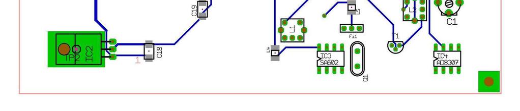
10 IV. Printed Circuit Board A. General The printed circuit board (PCB) has circuit traces and components on both top and bottom (see photos of completed PCB at end of this section). The component locations are silkscreened on the PCB. To aid construction, a layout and location grid is provided in Appendix A. Tables are provided in par. B and C below show the grid location for each component. Management of the work will be aided by printing the PCB layouts and then marking each component location with a colored marker pen as it is installed. Tools: Temperature-controlled soldering iron set to C 0.05 in (0.4 mm) diameter solder SMT soldering tools Regular soldering tools Magnifying goggles or visor B. Surface Mount Technology Parts Installation SMT PARTS ARE ALMOST IMPOSSIBLE TO RE-IDENTIFY VISUALLY IF THEY ARE ACCIDENTALLY MIXED TOGETHER. TO KEEP THIS FROM HAPPENING, DO NOT REMOVE THE SMT COMPONENTS FROM THEIR RECLOSABLE BAGS UNTIL YOU NEED THEM, AND SOLDER ALL COMPONENTS FROM A GIVEN BAG BEFORE OPENING ANOTHER BAG. Install all listed components on the top or bottom of the PCB as indicated. It is easier to install the physically lower components first, followed by higher components in stages until the highest components are installed last. There are 67 SMT components and installation time is between.5 and 3 hours. Work slowly and methodically to avoid costly mistakes. Solder all SMT resistors in the order given in the parts list Solder all SMT capacitors except C8, C9, C36 and C37 in the order given in the parts list After all other capacitors are soldered, install C36 and C37 (3528 form factor) followed by C8 and C9 (6032 form factor). C8, C9, C36 and C37 are tantalum capacitors and are polarity sensitive. Be sure they are oriented properly. The POSITIVE electrode is indicated by a silver bar on the top of the capacitor and slightly rounded terminal on the bottom. The PCB silkscreen does not indicate polarity so pre-mark polarity locations for these capacitors with an indelible marking pen. See PCB images at end of this sub-section. Solder all SMT inductors Required parts: Parts list ID Qty Description PCB location R8, R2, SMD-R 3 5 ohm, 0805 Bottom R6, R ohm, 0805 Bottom R9 330 ohm, 0805 Bottom R, R ohm, 0805 Bottom R9, R20, R5 3.0k ohm, 0805 Bottom R3, R4 2.5k ohm, 0805 Bottom R5 0k ohm, 0805 Bottom File: CALLISTOConstruction.doc, Page 8
11 R 20k ohm, 0805 Bottom R0 8k ohm, 0805 Bottom R7 22k ohm, 0805 Bottom R4, R6 2 56k ohm, 0805 Bottom R7, R8, R k ohm, 0805 Bottom R2, R22 2.0M ohm, 0805 Bottom R24 27k ohm, 0805 Bottom C2, C3, C4, C5, C6, C7, C3, C4, C5, C20, C2, C23, C24, C25, C26, C27, C28, C3, C32, C33, C34, C F, 0805 Bottom Bottom Bottom Bottom Bottom Bottom Bottom Bottom C0, C6, C nf (0.00 F), 0805 Bottom C39 See Table Note 50 pf, 0805 Bottom C8 5 pf, 0805 Bottom C29, C pf, 0805 Bottom C 27 pf, 0805 Bottom C7 33 nf (0.033 F), 0805 Bottom C9, C pf, 0805 Bottom C36, C F, 3528 Bottom C8, C F, 6032 Top L3, L4, L H, 20 Top L5.5 H, 20 Top L7 47 nh (0.047 H), 20 Bottom Indicates pay attention to polarity or direction Table Note: If your kit is supplied with C, pf trimmer capacitor (orange body), install C39. If your kit is supplied with C, pf trimmer capacitor (black body), DO NOT install C39. Location Grid (T = Top, see Appendix A for grid layout) R8-A3 R2-A3 SMD-R- A4 R6- B4C4 R25-B4C4 R9-A3 R-B3 R2-B3 R9-C2 R20-C2 R5-A3 R3-A2 R4-A2 R5-C2 R-C3 R0-A4 R7-A3 R4-C2 R6-A4 R7-B2 R8-B2 R23-B3 R2-B2 R22-B R24-B3 C2-A C3-A C4-B3 C5-A4 C6-A3 C7-A4 C3-A4 C4-A4 C5-A4 C20-A3 C2-A3 C23-C C24-C2 C25- B3C3 C26-C4 C27-B2 C28-C2 C3-B4 C32-B3 C33-B3 C34-B4 C35-B2 C0-A3 C6-A4 C38-C2 C39-A4 C8-A3 C29-B3B2 C30-B3 C-A3 C7-A4 C9-A3 C2-A3 C36-C2 C37-B2 C8-A3T C9- A3T L3-BT L4-A2T L6-BT L5-A2T L7-C File: CALLISTOConstruction.doc, Page 9


12 C. Through-Hole Parts installation Install all remaining PCB components EXCEPT the integrated circuits IC through IC9 (these will be installed after the power supplies are tested). Use the same procedures as above shortest components first and tallest components last and install them in the order shown in the parts list. The diode D is polarity sensitive and must be installed with the proper orientation. The bar or stripe on one end of the diode indicates the cathode and it must correspond with the bar on the PCB silkscreen Cut two small paper insulators to place between the PCB and the two crystals Q and Q2 (to prevent their metal case from shorting to the PCB) In North American receivers s/n NA008 and later, crystal Q frequency is MHz and capacitor C is pf. In earlier receivers Q was MHz and C was pf. The variable capacitor C supplied with your kit may have two or three pins. If it has two pins install it with the flat side of the capacitor body as shown on the silkscreen If you use the supplied DIL sockets with the integrated circuits, be sure to orient the end with the alignment notch or dimple as shown on the PCB drawing. Before installing the sockets, check for bent pins The 4-position PCB header connector has polarizing slots. The connector supplied with your kit will have one slot in the middle of one side. Some connectors Orient FL so the marking is on this side also may have two slots on the other side. Be sure to orient the side with ONE slot as shown on the PCB drawing The 0.7 MHz bandpass filter FL is marked on one side (L0.7A). Install the filter so this marking is oriented as shown on drawing right The two IF transformers Land L2 can be installed in only one direction. Be sure they are placed in the correct positions: L is installed to the left of FL and L2 is installed to the right The 6- and 8-position PCB headers Kand K3 are unpolarized. After soldering, put a small dab of red fingernail polish on the PCB next to pin of both PCB headers (see PCB images above). This will be used to align the unpolarized connectors associated with interface Cable 2 and an In-System Programming (ISP) cable (the ISP connector is not required for normal operation but can be used for future firmware updating; see Appendix C). While you have the fingernail polish out, put a small dab on the corresponding end of the 8-pin connector in Cable 2 and on positive side of the power input terminal block KL File: CALLISTOConstruction.doc, Page 0
13 Electrolytic capacitor C22 is polarity sensitive and must be installed with the proper orientation. The bar marked on the side of the capacitor indicates the NEGATIVE lead, and the longest lead is the POSITIVE. Be sure to put the long lead in the hole marked with the + polarity Bend the leads on U2 and U6 so the TO-220 tab lies flat on the heatsink and PCB with the holes lined up. Spread a small amount of heatsink compound (not supplied) on the tab before mounting on the heatsink. Use 4-40 hardware (supplied) to secure the tab and heatsink. Insert the screw with a flat washer from the bottom of the PCB and place another flat washer, split lock washer and nut on the top. The larger heatsink goes with IC2 and the smaller heatsink with IC6 Required parts: Parts List ID Qty Description PCB Location D N4007 Top Q MHz, ±0 ppm, 8 pf Top Q MHZ, ±50 ppm, 20 pf Top C See Table Note Trimmer, 6 50 pf (black) Top T BF99 Top Socket, IC7 6-pin socket Top Socket, IC8 20-pin socket Top Socket, IC5 40-pin socket Top Socket, IC3, IC4, IC9 3 8-pin socket Top FL L0.7A bandpass filter Top Header PCB connector, K 6-pin, 2x3 Top Header PCB connector, K2 4-pin, 2x7 Top Header PCB connector, K3 8-pin, 2x4 Top Terminal block, KL 2-position, screw-clamp Top R3 S0K4 varistor (VDR) Top Fuse socket 2-pin socket Top Fuse.0 A, 250 V, radial Top L FM-. (black core) Top L2 FM-.0 (yellow core) Top C22 Top 470 F, 35 V, radial IC2, IC CT voltage regulator Top Heatsink (large), IC thermal resistance (22 mm) Top Heatsink (small), IC6 5.6 thermal resistance (6 mm) Top Heatsink compound Not supplied Machine screw x 3/8 in. Bottom Flat washer 4 Standard x #4 Bottom Split lock washer 2 Standard x #4 Top Hex nut Top Indicates pay attention to polarity or direction Table Note: Early kits were supplied with pf trimmer capacitor (orange body). Kits s/n NA008 and later are supplied with pf trimmer capacitor (black body). File: CALLISTOConstruction.doc, Page


14 Location Grid (T = Top, see Appendix A) D -C4T Q-A2T Q2-B2T C-AT T-AT IC7-B2BT IC8-C2T IC5-C3C2T IC3-A2T IC4-AT IC9-B3T FL-A2T K-B3T K2-CT K3-BT KL-C4T R3-C4T Fuse-C4T L-A2T L2-AT C22-C4T IC2-A4T IC6-C4C3T D. Check Installation Double-check all components for location and check polarity sensitive components (electrolytic capacitors, diodes), voltage regulators and integrated circuit sockets for proper orientation. Double-check all soldering with a bright light and magnifying visor or magnifying glass Double-check that the fuse is installed Pictures of PCB bottom and top after all components have been installed (below) File: CALLISTOConstruction.doc, Page 2
15 V. Power Supply Tests A. Power Source The power supply components are now ready to test. You will need a nominal 2 Vdc power supply. The power supply or ac adapter should have the following characteristics Output voltage: 9 to 5 Vdc when under load Output current: 500 ma AC power adapters are a huge source of problems because they generally are very cheap and many are poorly designed. If you purchased your CALLISTO Receiver Kit with an optional ac adapter (North America customers only), you received a quality brand with sufficient capacity and well-filtered output. If you supply your own ac adapter for the receiver only and no focal plane unit control, its output must be rated at least 9 Vdc, 500 ma. AVOID ac adapters that use switch-mode technology (they generally are electrically very noisy). DO NOT attempt to power the CALLISTO receiver with an under-rated or lowquality ac adapter. DO NOT use an ac adapter with an output higher than approximately 5 Vdc when under load. The 7805 voltage regulators have a maximum input voltage rating of 35 Vdc but you should allow for a margin of /2. Similarly, the CALLISTO input current draw is approximately 255 ma (fully built with integrated circuits installed and in measurement mode) but you should allow for a margin of at least 2. Note: For reference, each of the six FPU control pins on the FPU connector can source up to 35 ma. Thus, for the situation where the receiver controls a focal plane unit, the receiver can draw its normal operating load plus a maximum of 20 ma additional load for the FPU control. The worst-case load would be approximately 465 ma and the power supply should be rated at least.0 A. However, for receiver testing purposes you only need a 500 ma power supply. Check your ac adapter leads for polarity with a voltmeter before connection. If you connect the power adapter backwards, you probably will not hurt anything but, of course, the receiver will not work. The PCB includes a reverse polarity guard diode (D) and a fuse (Fuse). The North American version of the receiver uses a coaxial dc power input jack (2. mm x 5.5 mm). The center pin of the coaxial power connector is positive. The ETH version of the receiver uses a DIN connector for dc power input. B. Voltage and Current Tests Tools: Digital multimeter (DMM) or analog multimeter Be sure the PCB is not sitting on a conductive surface. Configure the multimeter to measure dc current and connect it between the 2 Vdc power supply and the KL terminal block on the PCB (illustration below). Check your setup and then plug the power supply into an ac receptacle. Measure the dc load current. It should be as shown in the table on the next page. If the current is significantly higher than the range shown, there is a short circuit (for example, solder bridge) or faulty component. If the current is significantly lower, there is an open circuit (for example, cold solder joint) or faulty component. File: CALLISTOConstruction.doc, Page 3
 lead to ground (for example, the tab on IC2 or IC6 or the negative terminal of KL terminal block) and then probe the measurement points with the meter positive")
16 Reconfigure the multimeter to measure dc voltage. With the multimeter set to the 20 Vdc range, check voltages with respect to ground. Connect the meter negative (black) lead to ground (for example, the tab on IC2 or IC6 or the negative terminal of KL terminal block) and then probe the measurement points with the meter positive (red) lead. All voltage measurements may be made from the top of the PCB except IC. Refer to illustration and tables below. Nominal input current ~ ma dc Measured range 0 2 ma Remarks No load from integrated circuits Nominal voltage +5 V dc +2 V dc to V +9 to +5 V Determined by 7805 voltage regulator Actual input voltage at KL and actual input voltage less ~0.7 V at other points +2 Vdc +5 Vdc pin Vdc PIN 7,8 +2 Vdc +5 Vdc pin 6 +5 Vdc PIN 0 +5 Vdc +5 Vdc pin 2 +5 Vdc PIN 3 +5 Vdc PIN +5 Vdc pin 8 +5 Vdc pin 6,7 +5 Vdc +2 Vdc If all voltages and load current are within the specified ranges, the power supply components are working properly. Remove the dc power before continuing! File: CALLISTOConstruction.doc, Page 4
17 If the voltages or load current are not within the specified ranges, check for shorts, solder bridges and orientation of polarity sensitive components (electrolytic and tantalum capacitors, diodes, and voltage regulator ICs). Do not continue until you have fixed the problem. IC IC (CD36LS/IV-3) IC2 (7805) IC3 (SA602) IC4 (AD8307) IC5 (ATmega6) IC6 (7805) IC7 (MAX232) IC8 (74HC244) IC9 (25LC320) Ground pin Case Vcc pin (+5 Vdc) 2, 3 (output) 8 6, (output) , 7, 8 Vcc Source IC2 Pin is input (+2 Vdc) IC2 IC2 IC6 Pin is input (+2 Vdc) IC6 IC6 IC6 File: CALLISTOConstruction.doc, Page 5

18 VI. Install the Integrated Circuits A. General Use anti-static protection (grounded wrist strap) when handling the integrated circuits. Do not remove them from the anti-static pad until you install them on the PCB. B. Tuner IC IC must be installed on the top of the PCB and oriented with the coaxial connectors pointed toward the end of the PCB where the voltage regulators (IC2 and IC6) are located. One ground tab on the bottom corner of the tuner is slightly larger than the other three and it may be necessary to file a small slot in the hole on the PCB for that pin (use a thin jeweler s file). Do not force IC into the PCB. After inserting the tuner in the PCB, tack-solder two ground tabs, one in each corner. Lightly press the tuner case against the PCB and quickly resolder the two tabs to make sure the tuner is completely seated on the PCB and is perfectly vertical. After you are sure it is properly seated, solder the other two ground tabs and then the 5 power/input/output pins. Filling the ground tab holes with solder is NOT recommended (if you ever have to remove the tuner, you will regret having filled the holes with solder). Required parts: Parts List ID Qty Description IC CD36LS/IV-3 tuner Indicates pay attention to polarity or direction FROM THIS POINT FORWARD, DO NOT HANDLE THE INTEGRATED CIRCUITS AND PCB UNLESS YOU ARE WEARING ANTI-STATIC PROTECTION. C. Remaining Integrated Circuits Plug in the remaining integrated circuits, being sure they are oriented properly in their sockets. The sockets and ICs have a notch or dimple at one end, and they must line up. Now, just for fun, go back and check all the ICs for proper orientation. Note: Most ICs are shipped with the leads at a slight angle away from the body. It is much easier inserting them into a socket by first carefully bending the leads so they are at right-angles to the body. To do this, grip the IC at both ends and lay one side of the IC and pins on a hard, flat, smooth surface. Carefully rotate the body toward the pins a few degrees so the pins are uniformly bent at a right angle to the IC body. Flip the IC over and repeat on the other side. File: CALLISTOConstruction.doc, Page 6
19 Required parts: Parts List ID Qty Description IC3 Mixer SA602A (see Note) IC4 Log detector AD8307 IC5 Microprocessor ATmega6-6PU IC7 Transceiver MAX232EIN IC8 Buffer 74HC244 IC9 EEPROM 25LC320 Indicates pay attention to polarity or direction D. Check Installation Double-check all components for location and check polarity sensitive components (electrolytic capacitors, diodes), voltage regulators and integrated circuits and sockets for proper orientation Triple-check all soldering with a bright light and magnifying visor or magnifying glass Double-check location and orientation of integrated circuit in their sockets E. Test Power Supplies with ICs Installed Repeat the tests described in Sect. VI except use the table below. Nominal voltage +5 V dc +2 V dc Measured range to V +9 to +5 V Remarks Determined by 7805 voltage regulator Actual input voltage less ~0.7 V Nominal current ~230 ma dc ma Load current does not include the front panel LED. Load increases with CPU activity (for this test, the CPU is not active) If all voltages and load current are within the specified ranges, there are no major short circuits. Remove the dc power before continuing! If the voltages or load current are not within the specified ranges, check that all integrated circuits are installed correctly and there are no bent pins. To check for bent pins you will need to remove the ICs from their sockets. Also, check for shorts, solder bridges and orientation of polarity sensitive components (electrolytic and tantalum capacitors, diodes, and voltage regulator ICs). Although you already checked these devices, check them again. Do not continue until you have fixed the problem. File: CALLISTOConstruction.doc, Page 7
20 VII. Cables and Panels A. General Several cables are used in the CALLISTO receiver including: Cable Focal plane unit interface cable Cable 2 Serial interface, clock and detector output cable Cable 3 RF input cable Cable 4 Internal power cable Cable 5 External power cable Cables through 4 are associated with the front and rear panels and, when constructed, one end of each cable is connected to panel-mounted components and the other end connects to the PCB. Note: If the CALLISTO Receiver will never be used with a Focal Plane Unit or with an External Clock source, the associated cables and connectors do not need to be installed. Elimination of the FPU cable (Cable ) alone will reduce build time by a couple hours. Tools: Soldering iron set to C 0.03 in (0.8 mm) diameter or smaller solder Electronic construction hand tools including screwdrivers and assorted small hex nut drivers in non-metric sizes Magnifying goggles or visor B. Internal focal plane unit Cable Interface Cable uses a polarized 4-pin header connector at the PCB end and DB-25F connector at the rear panel end. The header connector and ribbon cable are preassembled. Strip, solder and connect the blunt end of the cable to the DB-25F connector as shown in the schematic below. An illustration showing the ribbon cable trimming pattern also is shown. A picture of the completed cable is shown at the end of this section. Plan your work and trim the ribbon cable so that it has enough slack to allow the rear panel to be removed for troubleshooting but not so much slack that it takes up a lot of space inside the enclosure. You can trim the cable by, say, 3.5 cm but check your own installation beforehand. Use the trimmings to make the ground bridge on pins 22 to 25. Heatshrink tubing is provided for the connections to the DB25F connector cut into 5 mm lengths. Mount the DB-25F on the rear panel as shown in the detail drawing below. The solder lug for grounding can be installed on the DB-9F connector in Cable 2 or the DB-25F connector.. File: CALLISTOConstruction.doc, Page 8
21 Required parts: Parts list ID K2 assy FPU Qty 2 Description Rear panel with cutouts Preassembled ribbon cable, 4C with header connector 4-40 jack screw set for D-sub connector DB-25F connector, solder cup Wire, 24 AWG, 300 V, green, 5 cm Heat shrink tubing, 0 mm Directions:. Place socket as shown (body in wide slot and key in narrow slot) 2. Slide ribbon cable in from right with red stripe toward far side 3. Drop press and compress until the socket latch clicks 4. Fold cable over top of connector and snap strain relief in position 50 IDC Adapter Block 3M p/n P IDC Socket Red stripe (pin ) Yellow stripe for Rainbow cable Pin 4C ribbon cable Polarizing Key 00 mm 0 mm 0 mm Wide slot 4C Cable Crimp Details File: CALLISTOConstruction.doc, Page 9
22 2x7 Top Ribbon cable, 28 AWG Red stripe Yellow stripe (rainbow cable) RearView 6 Cable DB-25F FPU ~ 28 AWG K2 Note position of polarizer C. Solder lug See also Cable 2 Rear panel chassis ground Green Solder wire & cable to DB-25F in following order: 3, 25 thru 6, 8 thru 3. Use heatshrink sleeves Internal interface Cable 2 Interface Cable 2 uses an unpolarized 8-pin header connector (K3) at the PCB end and various connectors at the rear panel end. A picture of the completed cable is shown at the end of this section. Using the provided socket contacts wire the header. If you do not use a crimping tool on the socket contacts, you must solder them. Do not rely on a mechanical crimp made with pliers without solder. Plan your work in the same way as Cable. All panel connectors in Cable 2 EXCEPT the BNC-F clock input connector mount from the rear of the panel. DO NOT solder the Trimming dimensions for coaxial cable to the BNC-F connector until you mount the connector connector K3 on the rear panel. ~4 mm LMR00A coaxial cable 3 mm Trimming dimensions for BNC-F ~9 mm LMR00A coaxial cable 5 mm After soldering one end, twist the individual wires together in groups as shown in the drawing. Do a neat job. Heatshrink tubing is provided for the connections to the DB-9F connector cut to length as required. The solder lug for grounding can be installed on the DB-9F connector or DB-25F connector in Cable. You may have to trim or file the solder lug on one side so that it fits properly on the back of the D-sub connector. Trim the LMR-00A coaxial cable used between connector K3 and the BNC-F connector as shown left. The center conductor is solid so after File: CALLISTOConstruction.doc, Page 20

23 crimping the socket contact for K3, apply a small amount of solder to reinforce the crimp. Be careful to not allow solder to wick up into to contact well or spring. Required parts: Parts list ID EIA-232 Clock Video K3 Qty Note header connector has no polarizer Description DB-9F connector, solder cup 4-40 jack screw set for D-sub connector BNC-F connector, front bulkhead mount Phone jack, mono, 3.5 mm Solder lug, #4 8-pin header connector, 2x4 Socket contact for header connector ( spare) Wire, 24 AWG, 300 V, green, 5 cm Wire, 24 AWG, 300 V, brown, 5 cm Wire, 24 AWG, 300 V, yellow, 5 cm Wire, 24 AWG, 300 V, blue, 5 cm Coaxial cable, LMR-00A, 5 cm Heatshrink tubing, 40 mm 3.5 mm mono Video output jack Twist together Cable 2 Blue T Alternate Jack Blue Green 2x4 Top T Green Shield Center LMR-00A coaxial cable BNC-F front bulkhead mount Clock input jack 3 Center R R RearView Green Yellow DB-9F EIA Brown K3 Twist together 6 Use heatshrink sleeves Green Solder lug D. Rear panel chassis ground (lug under D-Sub fastener) Internal RF input Cable 3 The RF input cable is supplied ready-built. Leave it in the plastic bag until directed to install it in Sect. VIII. Required parts: Parts list ID Qty Description RF input cable, N-F rear bulkhead RF Cable 3 mount connector to IEC PAL-M right angle connector File: CALLISTOConstruction.doc, Page 2
24 E. Installation on Rear Panel Mount the connectors for Cables, 2 and 3 on the rear panel. The drawing left shows the locations of the rear panel components (top). To keep from scratching or marring the panel, lightly tack some masking tape around the mounting holes and then tighten the hardware. Remove the tape when done and set aside the rear panel assembly. If you need to clean the panels, use a damp cloth; DO NOT use chemicals or else the silkscreen may dissolve. F. Internal power Cable 4 The internal power cable is a collection of interconnected parts mounted on the front panel with pigtails for connection to the PCB. Mount the components to the front panel and wire as shown in the schematic below. A drawing that shows the location of the connectors and controls on the front panel is provided left. Use the short 4-40 x 7/32 in machine screw to mount the turret terminal and solder lug as shown in the detail drawing below. The LED and coaxial power jack are slipped in their respective cutouts from the front of the panel, so do not connect them until they are mounted. The LED is press-fit. The tantalum capacitor, It is suggested that the plug be inserted in the coaxial power jack before wires are soldered to the jack this will help minimize distortion of the jack plastic insulator if you use too much heat. C-P is polarity sensitive, and the positive (+) terminal is indicated on the body (look with magnifier) and is the longest lead. Cut all leads as short as possible to minimize RFI coupling to and from the power supply. When finished, set aside the front panel assembly. Required parts: Parts list ID Qty Description Front panel with cutouts Turret terminal, 0.42 in x 4-40 x 0.25 in thread depth. Machine screw, 4-40 x 7/32 in Split washer, #4 Solder lug, #4 Switch SPDT miniature toggle switch, On-Off LED LED, Green, with internal resistor and leads Power Coaxial power jack, 2. mm x 5.5 mm C-P Capacitor, tantalum, 0 μf, 35 V C2-P Capacitor, ceramic, 0.0 μf, 50 V Wire, 24 AWG, 300 V, red, 5 cm Wire, 24 AWG, 300 V, black, 5 cm Indicates pay attention to polarity or direction File: CALLISTOConstruction.doc, Page 22
 to minimize voltage drop for the length of cable needed (< 0.5 V).")
25 G. External power Cable 5 If you purchased the optional ac adapter, it is supplied with coaxial power connector installed and ready-for-use. If you plan to use your own power supply, a 2. mm x 5.5 mm coaxial plug is provided with the kit. Wire the plug center-positive and use a large enough wire (not supplied) to minimize voltage drop for the length of cable needed (< 0.5 V). A 2-conductor, stranded, 8 AWG (.0 mm dia.) cable is suitable for most installations. Picture of almost completed Cable (right) and Cable 2 (left). Neither cable has the solder lug installed and Cable 2 does not yet have the BNC-F connector installed. They will be installed when the parts are mounted on the panel. File: CALLISTOConstruction.doc, Page 23

26 VIII. Assemble the Enclosure A. General The enclosure consists of top and bottom sections and front and rear end panels. Assembly consists of installing the PCB, connecting the cables on the end panels and installing screw fasteners to hold the assembly together. B. Assembly Tools: Phillips screwdriver, No. blade Torx screwdriver, No. T0 bit Slot screwdriver, /8 in (3 mm) blade Required parts: Parts list ID Qty Description Cable Focal plane unit interface cable from Sect. IV Cable 2 Serial interface, clock interface and detector output cable from Sect. IV Cable 3 RF input cable from Sect. IV Cable 4 Internal power cable from Sect. IV Front end panel, custom machined and labeled Rear end panel, custom machined and labeled Enclosure, two pieces, one shallow and one deep (note) 8 #4 x 3/8 in self-threading screws, Phillips pan head (note) 4 Stick-on rubber feet (note) Table note: The enclosure, as supplied by the Gie-Tec factory, includes two blank end panels, eight 2.9 x 9.5 mm self-threading screws and four rubber feet. The factory end panels are replaced by the custom machined end panels. The factory screws may require a Torx T0 driver or Phillips driver and may be replaced by the extra Phillips screws listed in the parts table. If you use the factory screws you will have to enlarge the corner holes in the end panels to 3.2 mm diameter. Before installation of the PCB and panels, run the self-threading screws in the corners of the upper and lower sections of the enclosure to cut the threads. Now, slide the PCB into the bottom section of the enclosure. If necessary, rub some candle wax on the edges of the PCB to help it slide easier. The bottom is the shallow section (see picture below). Plug the interface cables into their respective header connectors on the PCB. Cable connector is mechanically polarized and will fit only one way. Cable 2 connector is not polarized so you must be careful to match its pin with pin on the PCB header connector (the red dot made with fingernail polish). Do not force the connectors or you may damage the PCB. Connect the two power conductor pigtails from the front panel to KL on the PCB, observing File: CALLISTOConstruction.doc, Page 24


27 polarity: Red + and Black. DO NOT over-tighten the connector screws. The right-angle IEC PAL-M connector plug on Cable 3 plugs into the upper connector on the tuner IC. Dress the slack in this cable along the side of the PCB where the IF components are located. Check the mating interface between the top and bottom sections of the enclosure and you will notice that the rabbets (grooves) line up properly only one way. Place the top section on the bottom section and fasten the end panels to them using the No. 4 or factory supplied self-threading screws. Install the small stick-on rubber feet supplied with the enclosure on the bottom corners. After the enclosure has been fully assembled, apply power through the coaxial power connector on the front panel. The LED should glow green when the switch is turned on. Measure the receiver input current; it will be about 0 ~ 20 ma higher than listed in the table in Sect. VII (the added current is from the LED). Electrical and mechanical assembly is now complete. Go to the next section for final tests and adjustments. File: CALLISTOConstruction.doc, Page 25
28 IX. Receiver Test and Alignment A. General This section provides procedures to test basic receiver serial interface functionality including microprocessor operation and communication between the microprocessor and the front-end tuner. The CALLISTO Software Setup Guide provides detailed descriptions for setting up the receiver for actual operation. Tools: Non-metallic coil alignment tool, 2mm (3/32 in) blade Required parts: Parts list ID Qty Description EIA-232 cable, DB-9M/DB-9F, straight-through, 3 m long, shielded (optionally available) USB-serial adapter (if required) AC power adapter, 2 Vdc, 500 ma (user supplied or optionally available for North American customers) Antenna (see text) Connect a serial interface cable between the CALLISTO EIA-232 connector and the serial port on the computer or USB-serial adapter. Note: The cable uses only pins 2, 3 and 5 on the DB-9F and DB-9M connectors. The pins are wired straight-through as shown below. A shielded cable is recommended and it should be no more than 3 m long. If you ordered the optional cable with your receiver you received a quality shielded cable. A USB-serial interface adapter (optionally available) is required if your PC does not have a built-in serial port. If you use a USB-serial adapter, be sure that it is installed and working properly and that you are using the latest device drivers. DO NOT proceed until you have verified that you have the latest drivers. This is especially important if you are using Windows 7. Check for the latest drivers now. Note: It has been found that some USB-Serial Adapters built prior to deployment of Windows 7 do not work reliably even though the manufacturer has Windows 7 drivers available. If your serial connection is unreliable, try another, more modern adapter. For testing purposes, DO NOT connect the USB-serial adapter through a USB hub; connect the adapter directly to the PC. The CALLISTO Receiver has been tested with externally powered USB hubs but a hub should not be used at this time. If you have other USB devices connected to your PC, unplug them (except, of course, your USB mouse and keyboard if you have them) to avoid port conflicts. B. Setup HyperTerminal To test the EIA-232 serial port, it will be necessary to use a terminal emulator program. The following description uses HyperTerminal. File: CALLISTOConstruction.doc, Page 26
.")

. If you have multiple COM Ports in use, you can find the one associated with the USB-serial adapter by unplugging and then plugging it")

29 Start the HyperTerminal program (Start All Programs Accessories Communications) and create a new connection. Select File New Connection and type a name such as CALLISTO or e-callisto and click OK (see screenshots below). The Connect To window will pop up. Choose the appropriate COM Port from the dropdown list and click OK. If you are using a USB-serial adapter, this is the COM Port used by the adapter. To find the COM Port assigned to the adapter, go to Start Control Panel System Hardware Tab Device Manager and click the + next to Ports (COM & LPT). If you have multiple COM Ports in use, you can find the one associated with the USB-serial adapter by unplugging and then plugging it back in to the USB port while watching the Device Manager window. For now, unplug all other USB adapters and devices that use COM Ports (except, of course, the keyboard and mouse if they are connected via USB ports). A new COMx Properties window will pop up (below-left). Adjust the COM Port settings in the drop-down boxes as follows: 5200 Bits per second 8 Data bits Parity None Stop bits Flow control None. Click OK. File: CALLISTOConstruction.doc, Page 27

 is configured properly and the serial port is wired correctly, the HyperTerminal window should show $CRX: followed by the firmware version and")

30 In the Connection Properties, select the Settings tab and then ASCII Setup... The ASCII Setup window will open (below). Place checkmarks in the boxes and select the radio buttons as shown. These settings will ensure that the CALLISTO Receiver will respond to the ENTER key on the main keyboard. Otherwise, the ENTER key on the NUM keypad will have to be used. Click OK until you are back to the main window. Press the Call icon button on the HyperTerminal menu bar. Now, turn the receiver on or, if it was turned on, cycle the power. If the terminal emulator program (HyperTerminal) is configured properly and the serial port is wired correctly, the HyperTerminal window should show $CRX: followed by the firmware version and firmware date as shown. If the initial screen does not appear, leave the serial port connections and HyperTerminal as they are and cycle the power to the CALLISTO receiver. The firmware version in all North American CALLISTO Receivers is v.7 or later. If nothing happens, try unplugging the USB connector of the USB-serial adapter and plugging it back into the PC. There is considerable variability in USB-serial adapters leading to many problems. If you purchased an optional USB-serial adapter with your receiver kit, you received a quality adapter that is known to work with the CALLISTO Receiver. For additional serial port troubleshooting, use SysInternals PortMon program as described in Appendix B. File: CALLISTOConstruction.doc, Page 28

31 C. Test Receiver Basic Functions Query the Status of the CALLISTO Receiver by typing a question mark?, as shown below-left and then pressing ENTER. The status of various parameters should appear as shown below-right. There are many commands (a complete list is provided in an appendix in the CALLISTO Software Setup Guide) but for initial test purposes only a few more commands are used. One final test will verify that you can read the gain control voltage, 2nd IF amplifier bias voltage and input voltage. Type U2 +ENTER, U4 + ENTER and U6 +ENTER. When you press ENTER after each command, you should see the respective values on the screen. The actual values may vary from those shown left. The initial tests are now completed. Disconnect and close HyperTerminal. The next step is to align the st and 2nd IF transformers. D. IF Transformer Alignment The CALLISTO Receiver has two variable transformers L and L2 and a variable capacitor C used in the down-converter section. These are best aligned using a special software tool, simple.exe. The program Simple allows setting a test frequency, gain setting, and integration time. In order to use Simple, the CALLISTO Receiver must have passed the previous tests using HyperTerminal. D. Connect CALLISTO Receiver Connect the CALLISTO Receiver serial port to the PC, the RF Input connector to an antenna or a piece of wire (say 0.75 m long) and the power input to a 2 Vdc power source. See block diagram. Turn on the receiver. File: CALLISTOConstruction.doc, Page 29
.")

32 Be sure HyperTerminal or another program is not using the specified COM Port before proceeding to the next step. D.2 Simple Tool Setup Go to the Software folder on the CALLISTO CD and locate and open the file simple.zip. Extract the files to a folder on your PC (for example, c:\callisto\simple). Go to this folder and double-click on simple.exe (it must be run from the folder where its support files are located). The window that opens looks something like this: Set the COM port parameter to the serial port you are using with the receiver. The default values for the other parameters are suitable for alignment but you can change them if desired. The frequency used for IF transformer alignment is not critical. You use the background noise and not a signal for transformer alignment. Click Connect and you will notice changes to the voltage bar (see below). The voltage bar indicates the receiver output level. You can make minor adjustments to the height of the voltage bar with the Gaincontrol parameter the voltage bar should be about /3 ~ /2 height. You will adjust the transformers as described below for maximum indication on the voltage bar, so you may have to increase or decrease the Gaincontrol setting to achieve the best results. simple.exe, set the Com port and click Connect. If Simple opens but you cannot connect to the receiver (connection is indicated by an active voltage bar), close it by clicking the in upper-right corner or, if necessary, right-clicking simple.exe in Windows Task Manager and selecting End Process. Now, go to the folder that holds simple.exe and right-click on the file. Select the Compatibility tab and check Run this program in compatibility mode for: From the dropdown, select Windows 95. Click OK and restart Another feature of the Simple tool is the trigger pointer on the right. Left-click on the pointer and drag it up or down. As you slide the pointer up and down you will notice that the text changes to red or green. This helps you determine if the output voltage has increased or decreased. Initially, you will set the slider so that the text just turns red (RF < Trigger). Then, as you adjust the transformers and the output rises, the text will turn green (RF > Trigger). File: CALLISTOConstruction.doc, Page 30

33 D.3 Adjust st and 2nd IF Using a small non-metallic screwdriver (a metallic screwdriver will easily damage the transformer core caps and also interact with the settings), adjust the cores in both IF transformers L and L2 and the variable capacitor C for maximum output by observing the voltage bar in the Simple window. Be careful to not adjust C to an extreme position where there is a transition. A transition occurs every 80 deg. at maximum and minimum capacitance. The drawing right shows the capacitor at maximum value (small square imprints on adjustment screw lined up with triangle); minimum value is in the opposite direction. Try to find a compromise between C setting and IF transformer L2 setting. Slightly adjust C and then L2 for maximum. Slightly adjust C again and then L2 for maximum. Find a setting that results in the highest maximum. If a compromise setting cannot be found, it is possible that a different value is needed for C or C39. Stock values for North American receivers s/n NA0008 and earlier are: C = 6~50 pf (orange) and for C39 = 50 pf and for North American receivers s/n NA0009 and later are: C = 9~50 pf (black) and C = not used. After alignment, the yellow plastic cap on L2 core may protrude -2 mm above the metal can. L2 is a non-resonant transformer and its setting generally has only a minor effect on receiver output. DO NOT force L or L2 adjustable cores to the bottom of their range. When finished click the Disconnect button. You can leave Simple open for the next test. Leave the electromechanical setup as-is and go to the next step. E. Quick Video Output Test E. Setup Refer to illustration left. Connect mono or stereo headphones to the Video output jack on CALLISTO. Alternately, connect the Video output jack to the LINE IN jack or MIC jack of a PC soundcard. If you use a soundcard, be sure the appropriate input (LINE IN or MIC) is selected for Playback and the Speaker is not muted. In the example screenshot below, the soundcard is set to play from the LINE IN jack. Amplified speakers are required. Connect a wire antenna approximately 0.75 m long or an FM antenna to the RF Input jack on the receiver. E.2 Set Frequency of Nearby FM Broadcast Radio Station File: CALLISTOConstruction.doc, Page 3

34 Using Simple, set the frequency to the frequency of a nearby VHF-FM radio station. Alternately, you can use HyperTerminal as follows: Ensure that no programs are using the receiver COM Port. Run HyperTerminal and open the connection you previously saved. Enter the frequency of a nearby VHF-FM radio station using the F0x command, where x is the desired frequency in MHz. For example, say the desired station frequency is 04.5 MHz. Type F004.5 as shown at the bottom of the screen below-left and ENTER. This commands the receiver to tune to 04.5 MHz. You can confirm the setting by typing? followed by ENTER. You should see the Frequency parameter set to 04.5MHz as shown in the screen below-right. Using HyperTerminal, you can adjust the frequency in small steps by typing + or followed by ENTER. You may have to adjust the receiver gain. The Oxxx command is used to adjust the gain. The value of xxx ranges from 000 (zero gain) to 255 (maximum gain). Normal operating range is around 00 to 20. You can confirm the gain setting by using the U2 command (both Oxxx and U2 must be followed by ENTER). The voltage read by the command U2 is proportional to the gain setting value (see chart below). After the receiver frequency is set to the FM station, you should hear the radio signal (it may be distorted). If the test is successful, your CALLISTO Receiver is ready to use. Disconnect the audio cable. When finished with this test, be sure to remove the audio cable plug from the Video jack on the receiver. The cable capacitance affects the receiver integration time (the log detector output is not buffered). File: CALLISTOConstruction.doc, Page 32
35 Go to the CALLISTO Software Setup Guide. F. FPU Connector Tests The FPU connector (FC) wiring can be verified with the FC Test software tool. This tool sends FC codes to the receiver, which asserts the corresponding logic level on pins 6 through 2 of the connector. A logic high, corresponding to binary, is +5 V and a logic low, corresponding to binary 0, is 0 V. The logic levels may be measured on the respective pins of the FC with a digital multimeter. Alternately, a simple tester may be made from a DB-25M connector, six LEDs and six 330 ohm, /4 W resistors as shown right. See Appendix E for FC pin assignments and Appendix F for the FPU connector logic table. The six control pins in FC represents six bits with allowable decimal values 00 to 63. G. Optional Performance Tests See Appendix D H. Trouble Shooting If problems occur during testing, double-check the following: Current drawn by the CALLISTO Receiver Resistors are correct values and in their correct locations Diode correctly oriented and in its correct location Capacitors in their correct locations and electrolytic and tantalum capacitors oriented correctly IC sockets soldered properly and oriented correctly ICs oriented correctly in the sockets and no bent pins File: CALLISTOConstruction.doc, Page 33
36 No cold solder joints All pins soldered No solder bridges or shorts Power supply input voltage Voltage at the U2 and U6 voltage regulator outputs If no problems are found but the CALLISTO Receiver still does not test okay, contact us by File: CALLISTOConstruction.doc, Page 34

37 X. Circuit Description: For the following descriptions, refer to the block diagram and the schematic diagrams in this section. Enlarged printed circuit board layouts are provided at the end of this section. A. CALLISTO Receiver Block Diagram dc power input Voltage regulator for digital circuits Microprocessor and EEPROM FPU and clock buffer EIA-232 transceiver CD36LS/xx tuner Voltage regulator for RF circuits B. 2nd Mixer 2nd IF and log detector Receiver Front End The receiver front-end is a Philips Semiconductor CD36L-series television tuner. The European version is used, which has a 36.3 MHz IF output. This is called the st IF in the CALLISTO Receiver. Tuner operation is controlled by the microprocessor through the inter-integrated circuit bus, or I2C bus. The frequency can be changed in 62.5 khz steps with a step interval of.25 ms. File: CALLISTOConstruction.doc, Page 35
38 The tuner is compartmentalized and has three superheterodyne RF amplifier/mixer/oscillator sections, one each for low-band, mid-band and high-band operation. The CALLISTO Receiver uses the following band configurations: -band 45 ~ 75 MHz; Mid-band 75 ~ 450 MHz; and -band 450 ~ 870 MHz. The nominal RF voltage gain of the tuner is 47 db. The balanced narrowband IF output (7 MHz bandwidth as determined by the internal SAW filter) and the RF and IF gain control functions are used in the CALLISTO Receiver. A photograph of the tuner is shown below. This one was sacrificed when it was found to be incompatible with Callisto software. The front-end tuner gain is controlled by biasing the RF AGC and IF AGC inputs of the tuner. Voltage bias, and thus gain, is controlled by the microprocessor IC5, which, in turn, is set by software. Once set in software, the gain is fixed and not automatically adjusted in response to signal level (in other words, in the CALLISTO Receiver application, it is not an automatic gain control as implied by the nomenclature AGC). The microprocessor output (pin 2) is a pulse width modulated (PWM) waveform that is filtered by R2 and C9 to produce the dc bias for the RF AGC input. This dc bias is reduced by voltage divider R23 and R24 for the IF AGC input. In software, the PWM setting is a decimal value ranging from 0 (zero gain) to 255 (maximum gain). These correspond to an RF AGC voltage range of approximately.965 to Vdc and an IF AGC voltage range of to.93 Vdc. The gain control pulse period is a nominal 46 μs, corresponding to a frequency of about 2.7 khz. The duty cycle at a PWM setting of 0 is about 4% and at 240 is about 94% (see oscilloscope screenshots below for settings of 0, 00 and 240, respectively). File: CALLISTOConstruction.doc, Page 36

39 The voltages applied to the tuner RF AGC and IF AGC pins are proportional to the PWM setting in software. The chart below shows the relationship. A.2 2nd Mixer and IF The 2nd mixer and 2nd IF amplifier are part of the down-converter stage comprised of, in order of signal flow, transformer L, mixer/oscillator/amplifier IC3, crystal Q, bandpass filter FL, bipolar transistor T and transformer L2 plus bias and other power filter components. IC3 is the Philips Semiconductor SA602A mixer-amplifier integrated circuit. Note: A Philips Semiconductor SA602A is supplied with the kit but the SA62, SE62 and NE602 are identical and may be used in the receiver. The 36.3 MHz balanced IF output from the tuner IC is coupled to mixer IC3 through the primary winding of impedance matching transformer L. It has a primary: secondary turns ratio of :.5, providing an impedance ratio of :2.25. The output from the MHz crystal-controlled oscillator (Q) is mixed with the st IF to produce the 0.7 ±3.5 MHz 2nd IF, among other frequencies. The SA602A output is filtered by ceramic bandpass filter FL to eliminate all mixing products except the desired intermediate frequency. The receiver bandwidth is determined by ceramic filter FL. FL has a center frequency of 0.7 MHz ± 30 khz, nominal 3 db bandwidth of 280 ± 50 khz and 20 db bandwidth of 650 khz. Early versions of the receiver used a 27 MHz oscillator in the 2nd mixer, resulting in a 2nd IF frequency of 9.3 ± 3.5 MHz, which easily included the filter center frequency of 0.7 MHz. The output of FL is terminated by 330 ohm resistor R9 and coupled to the 2 nd IF amplifier by C6. The amplifier consists of a bipolar junction transistor T in a common emitter amplifier configuration. The amplifier output is terminated in impedance matching transformer L2. L2 has a primary: secondary turns ratio of 7:, providing an impedance ratio of 49:. The transistor bias components consist of R6, R7 and R8. The amplifier has a power gain of about 20 and its output is coupled through L2 to the log detector. File: CALLISTOConstruction.doc, Page 37
40 C. Logarithmic Detector The secondary (load side) of L2 is terminated by 5 ohm resistor SMD-R and ac coupled through C4 to the log detector IC4. IC4, an Analog Devices AD8307, provides a voltage output that is proportional to its power input, having a nominal gradient or slope of 25.4 mv/db. The analog output of the log detector is connected to a 0-bit analog-digital converter (ADC) in the microprocessor IC5, where it is converted to a digital stream and uploaded through the EIA-232 transceiver IC7 to the logging software on a PC. The log detector output also is connected to a phone jack on the rear panel. Note: Early versions of the CALLISTO Receiver have an 8-bit ADC but all North American versions have 0-bits. D. Power Supplies The nominal 2 Vdc input to the receiver is connected through terminal block KL. An on-board fuse Fuse and polarity guard diode D protect the receiver from overcurrent and wrong polarity. Two 7805 voltage regulators (TO-220 versions) IC2 and IC6 provide regulated +5 V ±5% for the analog RF circuits and digital logic circuits, respectively. The voltage regulators are lightly loaded but are equipped with heatsinks to draw heat away from the PCB. Filter inductors and capacitors and numerous decoupling capacitors are equipped to limit self-induced on-board radio frequency interference. E. Ancillary Functions The microprocessor IC5 can control a focal plane unit (FPU) through buffer IC8 and the FPU connector on the rear panel. Functions commanded through software control include testing, antenna polarization switching and noise calibrator switching. Up to 64 logic functions may be controlled through six lines. The control consists of a Vcc line and FPx line (see Appendix E for FPx and Vcc pin assignments and Appendix F for an FPU logic table). Typically, the Vcc line on the FPU connector supplies +5 Vdc to a TTL level interface in a focal plane unit. The FPx line is pulled high (+5 V) when asserted to logic and set low (0 V) when de-asserted to logic zero in software. When the receiver is powered up, all six lines are asserted logic high. The maximum drive current at each FPx line is 35 ma. The buffer IC8 also is used to couple an external MHz TTL level clock from the BNC-F connector on the rear panel to the microprocessor for precision time stamping of the data (Note: The external clock does not control the microprocessor clocking, it only controls data time stamping). These ancillary functions are equipped and functional in the North American version of the CALLISTO Receiver but the documentation presently does not provide specific details except as described in the next three sections, Appendix E and Appendix F. The ancillary functions are not required in the basic solar radio spectrometer system. File: CALLISTOConstruction.doc, Page 38
41 F. Configurations The diagrams left show the basic (or standard) CALLISTO Receiver configuration for linear polarization and a more advanced configuration using two receivers for circular polarization. The circular polarization setup requires a 90 deg. hybrid coupler, two antennas and two receivers. Two preamplifiers are optionally needed in systems that require additional gain. The hybrid coupler and preamplifiers typically would be installed at or near the antennas with preamplifier power fed through a bias-tee coupler or direct cable. G. Focal Plane Unit The Focal Plane Unit (FPU) derives its name from the instrumentation normally located at the focal point (feed point) of a large parabolic dish antenna. In e-callisto applications, it is not necessary to use a dish antenna. Other antenna types may be used, such as wideband log periodic antennas or even narrowband antennas. When the FPU includes noise calibration functions, it normally would be located as close as possible to the antenna to improve calibration accuracy. The basic configuration is shown below. Since the receiver provides a TTL level interface for FPU control, it may be necessary to use an FPU Cable Interface at each end to provide conversion of the TTL levels to levels compatible with the cable media used to carry the control signals to the FPU. Design of the FPU Cable Interface is beyond the scope of this manual. Additional details for control of the FPU are provided in the e-callisto Software Setup Guide. File: CALLISTOConstruction.doc, Page 39
42 G.. Noise Calibration Unit Referring to the drawing below, the upper configuration uses a directional coupler to couple the noise source and the lower configuration eliminates the directional coupler and is simpler. Rly Preamplifier Directional Coupler Out Term 50 ohm Rly 2a CALLISTO Receiver In Callisto 20 db Cpl 25 db 3 ~ 6 db Rly 2b Off (cold) 0 db Rly Noise Source 35 db ENR On (hot) Preamplifier CALLISTO Receiver Callisto 20 db Rly 2a 0 db Rly 2b Off (cold) 0 ~ 20 db Noise Source 35 db ENR On (hot) File: CALLISTOConstruction.doc, Page 40
43 H. Signal Chain The tables below show an estimate of the CALLISTO Receiver performance at 50 and 860 MHz for 7 m and 20 m antenna diameters. Performance estimate for 50 MHz Source: Unit Quiet Sun 7m Solar flux SFU.0 x 0 2 Antenna temperature K 2354 RF input power (W) W 9.0 x 0 5 RF input power (dbm) dbm 0.4 Attenuation (calibration) db 0.5 Preamplifier gain db m RG-23 at 50 MHz db 2.2 Philips tuner gain (min) db 4.0 2nd IF gain (nominal) db 20.0 Total gain db nd IF power output dbm 24. Log detector offset db 70.0 Log. detector output power dbm 45.9 Log detector slope V/dB Log detector output voltage V.67 ADC output (0 bit) Digit 682 Table Note: Data provided by Christian Monstein Quiet Sun 20m.0 x x Performance estimate for 860 MHz Source: Unit Quiet Sun 7m Solar flux SFU 8.2 x 0 20 Antenna temperature K 5298 RF input power (W) W 4.46 x 0 3 RF input power (dbm) dbm 93.5 attenuation (calibration) db 0.5 Preamplifier gain db m RG-23 at 860MHz db 9.0 Philips tuner gain (min) db 4.0 2nd IF gain (nominal) db 20.0 Total gain db nd IF power output dbm 4.0 Log detector offset dbm 70.0 Log. detector output power dbm 56.0 Log detector slope V/dB Log detector output voltage V.92 ADC output (0 bit) digit 787 Table Note: Data provided by Christian Monstein Quiet Sun 20m 8.2 x x Cold load Hot load x x Cold load Hot load x x Additional details: Antenna temperature: Solar flux x Antenna area /(2 x Boltzmann constant) + Tsystem K RF input power: Boltzmann constant x Antenna temperature x Bandwidth W Antenna area: (π x Diameter2)/4 Tsystem: 960 K (estimated) File: CALLISTOConstruction.doc, Page 4
44 Tuner-Receiver Schematic Diagram File: CALLISTOConstruction.doc, Page 42
45 Down-Converter Schematic Diagram File: CALLISTOConstruction.doc, Page 43
46 Logarithmic Detector Schematic Diagram File: CALLISTOConstruction.doc, Page 44

47 Processor Schematic Diagram File: CALLISTOConstruction.doc, Page 45
48 Power Supply Schematic Diagram File: CALLISTOConstruction.doc, Page 46


49 Printed Circuit Board Layout - Top File: CALLISTOConstruction.doc, Page 47


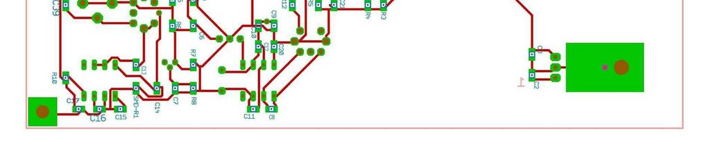
50 Printed Circuit Board Layout - Bottom File: CALLISTOConstruction.doc, Page 48
51 XI. Maintenance A. Purpose This section describes preventative maintenance that is performed to ensure the quality and reliability of data collected by the CALLISTO Receiver. The tasks are simple and routine and will keep your receiver and data in top condition. B. Monthly Preventative Maintenance Verify that the PC is synchronized with an internet time server Verify that the Scheduler file covers time of observation from actual sunrise to sunset and adjust as necessary Brush dust off the instrument being careful to not disturb the connections If additional cleaning of the enclosure and panels is required, use a damp cloth; DO NOT use any chemicals (or else the silkscreen may dissolve) C. Annual Preventative Maintenance Check the spectrum for noisy channels due to RFI. Update/edit the Frequency file to get the best channels with low RFI Check the capacity usage of the hard drive and delete old log files Defragment the hard drives used for Callisto and data storage Check for loose connectors and frayed insulation on cables Check power supply voltage, 9 ~ 5 Vdc If you use an external clock, check the amplitude and signal quality ( MHz, 5 V TTL signal) If you have access to a wide band noise source check the noise performance of the CALLISTO Receiver by applying about 5 db of excess noise to the input and analyzing the spectrum. Derive the noise figure of the instrument as follows (set gain to PWM = 200): ) Measure Vcold by applying a 50 ohm resistor to the antenna input and take a spectral overview (see CALLISTO Software Setup Guide); 2) Measure Vhot by applying the noise source to the antenna input and take a second spectral overview; 3) Calculate the Y-factor in db: Y(dB) = (V hot Vcold)/25.4 mv/db; 4) Convert Y-factor to linear ratio: Y = 0 [Y(dB)/0] 4) Derive the noise figure, NF, of the instrument from NF(dB) = ENR(dB) 0*log(Y-), where ENR is the excess noise ratio of the noise source adjusted for cable losses. NF should be less than 0 db without a preamplifier and less than about 3 db with an external low noise preamplifier. File: CALLISTOConstruction.doc, Page 49

52 Appendix A: Printed Circuit Board Layout and Location Grid Bottom Top C C B B A A File: CALLISTOConstruction.doc, Page 50
53 Appendix B: Using SysInternals PortMon Download PortMon here: Install PortMon and run. Generally, it will automatically monitor all equipped serial ports (COM Port) but you will need to check this. PortMon will not monitor a port if the port is busy when you start the program. Therefore, be sure HyperTerminal or other program is disconnected before opening PortMon. If necessary, refer to the PortMon Help for assistance setting up the program. PortMon will display and log (unless logging is shut off) all traffic on a serial port in both directions. When PortMon runs in logging mode for any length of time, say 2 hours or more, it will gradually use up all PC memory and you will notice that the hard drive continuously runs as Windows constantly swaps the cache between RAM and the hard drive. You also will notice the PC becomes sluggish and may appear to freeze (and probably has). Therefore, do not run PortMon in logging mode for more than an hour or two. To troubleshoot, compare your PortMon logs to those shown. The following log was obtained when the Connect button on HyperTerminal was pressed followed by the Disconnect button: Time Process CONNECT hypertrm.exe hypertrm.exe hypertrm.exe hypertrm.exe hypertrm.exe hypertrm.exe hypertrm.exe hypertrm.exe hypertrm.exe hypertrm.exe hypertrm.exe hypertrm.exe hypertrm.exe hypertrm.exe hypertrm.exe hypertrm.exe hypertrm.exe XonLimit:80 XoffLimit: hypertrm.exe hypertrm.exe hypertrm.exe hypertrm.exe DISCONNECT hypertrm.exe hypertrm.exe hypertrm.exe hypertrm.exe Request Port Result Other IRP_MJ_CREATE IOCTL_SERIAL_SET_QUEUE_SIZE IOCTL_SERIAL_CONFIG_SIZE IOCTL_SERIAL_GET_BAUD_RATE IOCTL_SERIAL_GET_LINE_CONTROL IOCTL_SERIAL_GET_CHARS IOCTL_SERIAL_GET_HANDFLOW IOCTL_SERIAL_GET_BAUD_RATE IOCTL_SERIAL_GET_LINE_CONTROL IOCTL_SERIAL_GET_CHARS IOCTL_SERIAL_GET_HANDFLOW IOCTL_SERIAL_SET_BAUD_RATE IOCTL_SERIAL_SET_RTS IOCTL_SERIAL_SET_DTR IOCTL_SERIAL_SET_LINE_CONTROL IOCTL_SERIAL_SET_CHAR IOCTL_SERIAL_SET_HANDFLOW ProlificSerial2 ProlificSerial2 ProlificSerial2 ProlificSerial2 ProlificSerial2 ProlificSerial2 ProlificSerial2 ProlificSerial2 ProlificSerial2 ProlificSerial2 ProlificSerial2 ProlificSerial2 ProlificSerial2 ProlificSerial2 ProlificSerial2 ProlificSerial2 ProlificSerial2 SUCCESS SUCCESS SUCCESS SUCCESS SUCCESS SUCCESS SUCCESS SUCCESS SUCCESS SUCCESS SUCCESS SUCCESS SUCCESS SUCCESS SUCCESS SUCCESS SUCCESS Options: Open InSize: 892 OutSize: 892 Size: 0 IOCTL_SERIAL_SET_TIMEOUTS IOCTL_SERIAL_SET_WAIT_MASK IOCTL_SERIAL_WAIT_ON_MASK IRP_MJ_READ ProlificSerial2 ProlificSerial2 ProlificSerial2 ProlificSerial2 SUCCESS RI:0 RM:0 RC:0 WM:0 WC:5000 SUCCESS Mask: RLSD ERR SUCCESS CANCELLED Length 80 IOCTL_SERIAL_SET_WAIT_MASK IOCTL_SERIAL_PURGE IRP_MJ_CLEANUP IRP_MJ_CLOSE ProlificSerial2 ProlificSerial2 ProlificSerial2 ProlificSerial2 SUCCESS SUCCESS SUCCESS SUCCESS Rate: 5200 StopBits: Parity: NONE WordLength: 8 EOF:0 ERR:0 BRK:0 EVT:0 XON: XOFF:3 Shake: Replace: Mask: RLSD ERR Purge: TXABORT RXABORT The following log was obtained by typing? and then ENTER:? 0 Time Process Request hypertrm.exe IRP_MJ_WRITE Port ProlificSerial2 SUCCESS ENTER hypertrm.exe IRP_MJ_WRITE ProlificSerial2 SUCCESS hypertrm.exe IRP_MJ_READ ProlificSerial2 SUCCESS elay=0msec.$crx:frequency=0.0mhz.$crx:sweeplength=0.$crx:low_ban hypertrm.exe IRP_MJ_READ ProlificSerial2 TIMEOUT X:mid_band_max=450MHz.$CRX:high_band_max=863MHz.$CRX:Idle=0x hypertrm.exe IRP_MJ_READ ProlificSerial2 SUCCESS $CRX:Debug=Off.$CRX:Trigger=No.$CRX:FPUcodex=0.$CRX:GS =62208.$C Result Other Length :? Length :. Length 80: Length 6: Length 80: File: CALLISTOConstruction.doc, Page 5

54 Appendix C: In-System Programming The ATmega6-6PU microprocessor IC5 provided with the kit is pre-programmed. It does not have a bootloader but it does support In-System Programming (ISP). The 6-pin connector K on the PCB is the ISP interface. Refer to the ATmega6-series microprocessor datasheet for ISP support. The microprocessor IC supplied with the kit was not programmed using the CALLISTO ISP interface. It was programmed as follows:. The firmware on the ATmega6 MPU consists of four separate.hex files: Lo-Fuse Hi-Fuse EEPROM Flash 2. A new MPU is programmed using AVRDude software, a shop-built USBTiny programmer, and a shop-built chip carrier platform with a Zero Insertion Force (ZIF) socket (left). The chip carrier platform has a 4 MHz crystal and associated load capacitors, which are necessary to verify the programming. Each.hex file is written in turn and then automatically verified. 3. Additional details available on request. File: CALLISTOConstruction.doc, Page 52
55 Appendix D: Basic RF Performance Tests A. The basic RF performance tests include five measurements. Gain Control Test 2. Bandpass Filter Test (Go/No-Go) 3. Noise Figure Test 4. Bandpass Filter Response Test. The resolution of this test is equal to the receiver tuning resolution of 62.5 khz 5. Minimum Discernible Signal Test B. Test hardware and software requirements. Noise generator (noise source) with a calibrated excess noise ratio (ENR) of 0 ~ 5 db across the frequency range of 45 to 870 MHz 2. RF signal generator that can be set within the receiver frequency range of 45 to 870 MHz. The output level does not have to be calibrated for the bandpass filter go/no-go test but it should be in the range of 80 to 60 db. However, for the minimum discernible signal test, the output must be calibrated. If the signal generator output is fixed, calibrated attenuators can be used to reduce the level 3. Terminal emulator program (example, HyperTerminal, see elsewhere in this manual) 4. Callisto software. Callisto software setup is covered in the CALLISTO Software setup Guide C. Gain Control Linearity Test. Open HyperTerminal and connect to receiver 2. Set PWM gain to different values (Oxxx) and read AGC voltage (U2); use PWM values of 00, 050, 00, 50 and After each PWM Value change, record the AGC voltage after it has stabilized (three readings in a row read the same voltage) 4. Plot AGC voltage vs PWM value (see example below) 5. Result: Linear 6. Disconnect HyperTerminal File: CALLISTOConstruction.doc, Page 53
 6. Adjust signal generator or Callisto frequency to peak level (for Callisto use + and keys); the peak will be broad.")
56 D. Bandpass Filter Test Go/No-Go. Open HyperTerminal and connect to receiver 2. Set PWM gain to 20 (O20) 3. Connect RF signal generator tuned to 50 MHz, 70 dbm 4. Set data format to decimal mv (%2) 5. Set Callisto to the same frequency (F050.0) 6. Adjust signal generator or Callisto frequency to peak level (for Callisto use + and keys); the peak will be broad. Measure and record frequency at peak and maximum detector voltage, Vmax (A0) 7. Set Callisto 48 MHz (F048.0) 8. Measure and record detector voltage, Vmin, low (A0) 9. Repeat for 52 MHz (F052.0), Vmin, high (A0) 0. Calculate dblow = [(Vmax Vmin, low)/25.4mv/db] and dbhigh = = [(Vmax Vmin, high)/25.4mv/db]. Result: dblow and dbhigh 38dB 2. Disconnect HyperTerminal E. Noise Figure Test. Connect unpowered (cold) noise source to receiver RF input and make other connections as shown below. Use high-quality coaxial cable and make it as short as possible. Be sure Noise Source power switch is in Cold (Off) position File: CALLISTOConstruction.doc, Page 54
57 Open Callisto and then click Edit callisto.cfg. Set [agclevel] parameter to 250. Noise figure is somewhat dependent on gain setting. Select Manual radio button. Click on Start measurement. Run for a moment to warm-up the receiver, and then select Stop measurement Save spectral overview with Callisto (this is the cold OVS) Apply power to noise source (hot), and Save spectral overview with Callisto (this is the hot OVS) Open Excel and load both OVS files (see note below) Calculate Y-factor in db, Y(dB) = [(Vhot Vcold)/25.4 mv/db] at each frequency Calculate Y-factor as a linear ratio, Y= 0[Y(dB)/0] at each frequency Calculate noise figure at each frequency, NF(dB) = ENR(dB) 0*log(Y ), where ENR is the excess noise ratio from the noise source calibration chart Plot NF(dB) vs frequency (MHz) Nominal result: 0dB across frequency band (somewhat dependent on gain setting [agclevel]). Expect reduced noise figure in middle-band and occasional spikes. Generally, there will be ± db variation around a nominal value. See example chart below File: CALLISTOConstruction.doc, Page 55
58 20 S/N NA008, PWM 200 Noise Source: Agilent 346B s/n 264A Noise Figure (db) Frequency (MHz) Note: An example Excel file (CALLISTO_NF.xls) is provided on the CD for calculating noise figure. Follow these steps to use this file: a. Open the noise figure spreadsheet CALLISTO_NF.xls and replace the values in column G with the ENR of your noise source at each frequency (to simplify, but with some accuracy loss, use one ENR for all frequencies). Be sure to adjust the ENR for cable losses (otherwise, the noise figure calculations will be overstated) b. Open cold OVS file with Excel. Select the Semicolon Delimeter and General Column data format. The OVS file has two columns, A is frequency (MHz) and B is measured output voltage (mv) of the log detector, which is proportional to power. Copy column B containing the voltage values to the Windows Clipboard. Paste the Clipboard to Column B of the noise figure spreadsheet c. Open hot OVS file with Excel using the delimiter and format as before. Copy column B voltage values to the Clipboard. Paste the Clipboard to Column C of the noise figure spreadsheet d. If necessary, update calculations (F9) e. Edit chart title and sheet name so you can identify it in the future. It is helpful for future reference to include the noise source model and serial number and receiver serial number and gain setting in the chart title f. To save the chart as an image, right-click the chart border and select Copy. Open Windows Paint or other image editing application and Paste. Use Save As... to save the image in your choice of file format and filename. F.. 2. Bandpass Filter Response Test Connect RF signal generator to RF Input; tune generator to MHz, 70 dbm, Carrier OFF (if the signal generator does not have a carrier ON/OFF control, initially substitute a 50 ohm termination on receiver RF input) Use Frequency Genie to produce a frequency file with 40 channels in a frequency range of 49 to 5 MHz. Save file using a recognizable filename (example, frq0050) and then copy it to the directory used by Callisto File: CALLISTOConstruction.doc, Page 56

![Set the [agclevel] parameter to a mid-range value, say 00 or 20, and set [db_scale]=4. Save the file Click on Start measurement Click the Spectrum y(f) button.](/docs-images/81/84621261/images/59-1.jpg "When the Spectrum y(f) window opens, select the Digits radio button (if not already selected); wait 5 seconds On the Spectrum y(f) window, select db Turn ON the signal generator carrier (or replace")
59 Open Callisto and select Manual mode. If necessary, press Stop measurements Press Load frequency file button on Callisto and then select the file produced and saved in step 2 From the Callisto menu bar, click on Edit callisto.cfg. Set the [agclevel] parameter to a mid-range value, say 00 or 20, and set [db_scale]=4. Save the file Click on Start measurement Click the Spectrum y(f) button. When the Spectrum y(f) window opens, select the Digits radio button (if not already selected); wait 5 seconds On the Spectrum y(f) window, select db Turn ON the signal generator carrier (or replace the 50 ohm termination with the signal generator output). After a moment the spectrum should appear as an individual spike at each frequency. Adjust the signal generator output so the spectral peaks are below the top of the graph. Alternately, adjust the [db_scale] or [agc_level] parameters in callisto.cfg. If [agc_level] is adjusted, click Stop measurement before changing and saving the parameter, then click Start measurement to resume testing The Spectrum y(f) chart (aboveright) shows a 62.5 khz resolution display of the receiver s frequency response On Callisto, click on the Spectrum y(f,t) button and then select Fixed BG (right). As the signal generator output is adjusted, the frequency response is shown on the Spectrum y(f,t) window as horizontal colored bands (next page, right) To measure Minimum Discernible Signal, go to par. G Note: The top window bar in the spectrographs show the default frequency file, which may be different than the file you separately loaded for the tests File: CALLISTOConstruction.doc, Page 57
 chart.")
60 G. Minimum Discernible Signal (MDS). Follow steps through in par. F above 2. Decrease signal generator output to around 00 or 0 dbm 3. Slowly decrease the signal generator output until the signal disappears into the random noise spikes seen on the Spectrum y(f) chart. Because of integration and sweep times, the display reacts rather slowly. Be patient. Slowly increase the signal generator output until the signal reappears. This provides a rough indication of the MDS. MDS is somewhat dependent on the receiver gain setting [agclevel]. As you decrease the signal generator output level, it may be necessary to change the [db_scale] parameter in callisto.cfg for better amplitude resolution. To increase the resolution, decrease the [db_scale] parameter and then Save the change. The change takes effect within about 5 seconds. The image right shows the Spectrum y(f) for a 20.0 dbm signal, which for the test receiver is a few db above the MDS (MDS will vary from receiver-to-receiver). Note that the five green signal spikes at the bottom of the chart around the center frequency of 50 MHz are near the height of the noise spikes on either side File: CALLISTOConstruction.doc, Page 58
Assembly Instructions for the 1.5 Watt Amplifier Kit
 Assembly Instructions for the 1.5 Watt Amplifier Kit 1.) All of the small parts are attached to a sheet of paper indicating both their value and id. 2.) Leave the parts affixed to the paper until you are
SoftRock v6.0 Builder s Notes. May 22, 2006
 SoftRock v6.0 Builder s Notes May 22, 2006 Be sure to use a grounded tip soldering iron in building the v6.0 SoftRock circuit board. The soldering iron needs to have a small tip, (0.05-0.1 inch diameter),
SoftRock v6.0 Builder s Notes. April 6, 2006
 SoftRock v6.0 Builder s Notes April 6, 006 Be sure to use a grounded tip soldering iron in building the v6.0 SoftRock circuit board. The soldering iron needs to have a small tip, (0.05-0. inch diameter),
Alaska geography e-callisto Solar Spectrometer Network CALLISTO Receiver system characteristics Construction Performance Conclusions
 1 Alaska geography e-callisto Solar Spectrometer Network CALLISTO Receiver system characteristics Construction Performance Conclusions 2 Mostly in the Western Hemisphere Part of it stretches into the Eastern
SoftRock v5.0 Builder s Notes. December 12, Building a QSD Kit
 SoftRock v5.0 Builder s Notes December 12, 2005 Building a QSD Kit Be sure to use a grounded tip soldering iron in building the QSD board. The soldering iron needs to have a small tip, (0.05-0.1 inch diameter),
V6.2 SoftRock Lite Builder s Notes. November 17, 2006
 V6.2 SoftRock Lite Builder s Notes November 17, 2006 Be sure to use a grounded tip soldering iron in building the v6.2 SoftRock circuit board. The soldering iron needs to have a small tip, (0.05-0.1 inch
Read This Page First
 Read This Page First If you are reading this you know the manuals are always available at QRPKITS.com. This is version 8.0 of the manual dated 4/27/2016. There is no need to print out the whole assembly
Pacific Antenna Low Pass Filter Kit
 Pacific Antenna Low Pass Filter Kit Description Many basic transmitter and/or transceiver designs have minimal filtering on their output and frequently have significant harmonic content in their signals.
Value Location Qty Potentiometers C1M Distortion 1 A10k Volume 1. Footswitch 3PDT SW1 1. Jacks 1/4 Mono 2 DC Power 1
 Distortion BUILD INSTRUCTIONS Thank you for your purchase of our Distortion+ kit! We have completely redesigned our entire line of kits to be the most user friendly, while still maintaining their same
Cricket 80a Assembly Manual v Copyright David Cripe NM0S The 4 State QRP Group
 Cricket 80a Assembly Manual v. 1.0 Copyright 2017 David Cripe NM0S The 4 State QRP Group Introduction Thank you for purchasing a CRICKET 80a Transceiver. We hope you will enjoy building it and find it
Building the Sawdust Regenerative Receiver
 Building the Sawdust Regenerative Receiver Introduction The Sawdust is a super regenerative receiver using the basic Armstrong design architecture. The receiver uses one toroidal transformer to provide
Pacific Antenna Field Strength Indicator Kit
 Pacific Antenna Field Strength Indicator Kit Description The Field Strength Indicator kit from Pacific Antenna provides a visual way to monitor the presence and relative strength RF fields through the
Bill of Materials: PWM Stepper Motor Driver PART NO
 PWM Stepper Motor Driver PART NO. 2183816 Control a stepper motor using this circuit and a servo PWM signal from an R/C controller, arduino, or microcontroller. Onboard circuitry limits winding current,
BP-1A. Band-Pass variable filter continuous tuning from 3 to 30MHz. For analogue or software-defined receivers (SDR) Assembly manual
 Assembly manual") BP-1A Band-Pass variable filter continuous tuning from 3 to 30MHz. For analogue or software-defined receivers (SDR) Assembly manual Last updated: December 1, 2017 ea3gcy@gmail.com Updates and news at:
BP-1A Band-Pass variable filter continuous tuning from 3 to 30MHz. For analogue or software-defined receivers (SDR) Assembly manual Last updated: December 1, 2017 ea3gcy@gmail.com Updates and news at:
QRPGuys Michigan Mighty Might Plus 40M Transmitter
 QRPGuys Michigan Mighty Might Plus 40M Transmitter First, familiarize yourself with the parts and check for all the components. If a part is missing, please contact us and we will send one. You must use
Pacific Antenna Easy Transmitter Kit
 Pacific Antenna Easy Transmitter Kit Introduction The Easy Transmitter kit from qrpkits.com provides a crystal controlled transmitter with VXO tuning. The circuit consists of a N3904 based crystal oscillator
Xkitz.com XLO-5CP Control Panel for Five Channel Color Light Organ
 Xkitz.com XLO-5CP Control Panel for Five Channel Color Light Organ Rev 1.15 An Optional accessory for the Xkitz XLO-5 or XLO-5DC 5 Channel Color Light Organs Introduction This kit contains all the electronics
Building the Sawdust Regenerative Receiver
 Building the Sawdust Regenerative Receiver Introduction The Sawdust is a super regenerative receiver using the basic Armstrong design architecture. The receiver uses one toroidal transformer to provide
Easy Transmitter. Support ETX_REV5_Manual V2.7 Revised
 Easy Transmitter Introduction The Easy Transmitter kit from qrpkits.com provides a basic, crystal controlled transmitter with VXO tuning to provide a small tuning range around the crystal frequency. It
Custom Front Panel Upgrade Instructions
 Custom Front Panel Upgrade Instructions Here are the directions for upgrading your SP-II to an SP-IIB, with a custom blackanodized front panel and engraved lettering. There are only forty SP-IIB s in existence
Assembly Instructions
 Assembly Instructions For the SSQ-2F 3.1 MHz Rife Controller Board Kit v1.41 Manual v1.00 2012 by Ralph Hartwell Spectrotek Services GENERAL ASSEMBLY INSTRUCTIONS Arrange for a clean work surface with
Assembly Instructions for the FRB FET FM 70 Watt Amp
 Assembly Instructions for the FRB FET FM 70 Watt Amp 1.) Orient the circuit board with the diagram 2.) Use a narrow chisel tip 25-30 watt soldering iron for assembly 3.) All the small parts are taped onto
Read This Page First
 Read This Page First If you are reading this you know the manuals are always available at QRPKITS.com. If you have questions contact qrpkits.com@gmail.com There is no need to print out the whole assembly
S-Pixie QRP Kit. Student Manual. Revision V 1-0
 S-Pixie QRP Kit Student Manual Revision V 1-0 Introduction The Pixie 2 is a small, versatile radio transceiver that is very popular with QRP (low power) amateur radio operators the world over. It reflects
PAC-12 Kit Contents. Tools Needed Soldering iron Phillips screwdriver Wire stripper Wrenches, 7/16 and 1/2 Terminal crimp tool Pliers Solder
 PAC-2 Kit Contents Part Quantity Screws: 8/32 x 3/8 Screws: 8-32 x 5/6 Screw: 8-32 x /4 #8 internal tooth washers #8 solder lug ring terminals Bolt: Aluminum, /4-20 x.5 /4 internal tooth washer Nut: Aluminum
DEM Part Number L144-28INTCK 144 MHz Transverter Kit and complete kit
 DEM Part Number L144-28INTCK 144 MHz Transverter Kit and complete kit Power Out: Noise Figure and Gain: DC Power Requirement: 50 mw linear minimum 3.5 db NF nominal, 5 dbg maximum 12-15.5 VDC, 13.8 nominal
LED Field Strength Indicator Kit
 LED Field Strength Indicator Kit Description The Field Strength Indicator kit from Qrpkits.com provides a visual way to monitor RF fields through the brightness of an LED. It will respond to RF fields
Value Location Qty Transistors 2N5485 Q1, Q2, 4 Q3, Q4 2N5087 Q5 1. Trim Pots 250k VTRIM 1. Potentiometers C500k Speed 1. Toggle Switch On/On Vibe 1
 P-90 BUILD INSTRUCTIONS Thank you for your purchase of our P-90 kit! We have completely redesigned our entire line of kits to be the most user friendly, while still maintaining their same great sound!
LDB-1 Kit Instructions Page 1 of 8
 LDB-1 Kit Instructions Page 1 of 8 Important Information Congratulations and thank you for your purchase of the LDB-1 Little Drummer Boy Analog Drum Machine Kit! Before you start, please read the enclosed
MP573 Assembly guide. Soldering. MP573 Assembly guide PCB split PCB split. Document revision 2.2 Last modification : 22/08/17
 MP573 Assembly guide Safety warning The kits are main powered and use potentially lethal voltages. Under no circumstance should someone undertake the realisation of a kit unless he has full knowledge about
Build this Direct Digital Synthesizer "Development Kit" By: Diz Gentzow, W8DIZ
 Build this Direct Digital Synthesizer "Development Kit" By: Diz Gentzow, W8DIZ A great tutorial for adding a keypad to the DDS Kit by Bruce, W8BH This manual has been prepared to be read directly on screen.
Eurorack DIY Kit Instructions. All Thonk kits are sold under our standard Terms and Conditions -
 MA VCA OVERVIEW For the most recent version of this document please visit http://thonk.co.uk/documents/ma/ For all technical support please visit http://bit.ly/1tl78e0 on Muffwiggler. All Thonk kits are
HT-1A Dual Band CW QRP Transceiver. Kit Building Instructions
 HT-A Dual Band CW QRP Transceiver Kit Building Instructions Rev B, July 8, 08 Designed by BD4RG Exclusively distributed by CRKITS.COM and its worldwide distributors Join the group http://groups.io/g/crkits
OpenROV. Guide 3 - Electronics. We will now move to the assembly of the electronics that will control the ROV. Written By: OpenROV
 OpenROV Guide 3 - Electronics We will now move to the assembly of the electronics that will control the ROV. Written By: OpenROV 2017 openrov.dozuki.com Page 1 of 33 INTRODUCTION We will introduce soldering
SDR Cube Transceiver Online Assembly Guide
 SDR Cube Transceiver Online Assembly Guide Detailed construction notes for building and testing each of the SDR Cube kit modules Home Bill of Materials I/O Board Controls Board DSP Board Softrock SR-Base
MICROGRANNY v2.1 - Assembly Guide
 last update: 9. 5. 2017 MICROGRANNY v2.1 - Assembly Guide bastl-instruments.com INTRODUCTION Welcome to the assembly guide for the MicroGranny kit. MicroGranny is a monophonic granular sampler by Bastl
Read This Page First
 Pacific Antenna 0 Watt HF Amplifier Kit Manual This is Version 5.5 dated 060505 Read This Page First If you are reading this you know the manuals are always available at QRPKITS.com. If you have questions
LITTLE NERD v1.1 Assembly Guide
 last update: 9. 3. 2016 LITTLE NERD v1.1 Assembly Guide bastl instruments.com INTRODUCTION This guide is for building Little Nerd module from Bastl Instruments. It is good to have basic soldering skills
Construction Guide European Version
 Construction Guide European Version PCB This section describes how to build up the DRO-350 printed circuit board (PCB). The bare PCB is available for purchase on the order page. Static Protection Bare
Manual Version July 2007
 Manual Version 1.2 - July 2007 Page 1 Table of Contents Section1: M3 Phono Board Build...3 Phono Board Parts List...3 Preparation...4 Fitting the Valve Bases...6 Installing the Resistors...7 Starting the
NEW DESIGN***DEM Part Number FRS***NEW DESIGN Low power 144 MHz Transverter for the Flex Radio System SDR-1000 Operating Specifications:
 NEW DESIGN***DEM Part Number 144-28FRS***NEW DESIGN Low power 144 MHz Transverter for the Flex Radio System SDR-1000 Operating Specifications: Operating Voltage: 12.0-15.5 VDC, 13.8 nominal Current Drain:
Pacific Antenna Easy TR Switch
 Pacific Antenna Easy TR Switch Kit Description The Easy TR Switch is an RF sensing circuit with a double pole double throw relay that can be used to automatically switch an antenna between a separate receiver
PM124 Installation Instructions. See important note about revisions of this board on the last page.
 Marchand Electronics Inc. PO Box 473, Webster, NY 14580 Tel:(716) 872-0980 Fax:(716) 872-1960 info@marchandelec.com http://www.marchandelec.com (c)1997 Marchand Electronics Inc. PM124 Installation Instructions
The Wave (K-MOD103) GUITAR DWELL REVERB REVERB SWITCH ON OUT OFF
 GUITAR DWELL REVERB REVERB SWITCH ON OUT OFF") The Wave (K-MOD103) OUT IN GUITAR IN DWELL REVERB REVERB SWITCH ON GUITAR OUT POWER ON OFF OFF Please note, there are no labels for this kit. The controls, switches and connectors have only been labeled
The Wave (K-MOD103) OUT IN GUITAR IN DWELL REVERB REVERB SWITCH ON GUITAR OUT POWER ON OFF OFF Please note, there are no labels for this kit. The controls, switches and connectors have only been labeled
Pacific Antenna - Easy TR Switch
 Pacific Antenna - Easy TR Switch Kit Description The Easy TR Switch is an RF sensing switch that can be used to switch an antenna between a receiver and transmitter. It also has a second switched pair
Pacific Antenna 10 Watt HF Amplifier Kit
 Pacific Antenna 0 Watt HF Amplifier Kit Description Our 0 watt Linear, HF amplifier kit is designed to increase the power output of low power transmitters. Gives up to 5dB gain and includes an input attenuator
Wiring Manual NEScaf April 2010 (August 2006)
") Wiring Manual NEScaf April 2010 (August 2006) Switched Capacitor Audio Filter The NEScaf is a switched capacitor audio filter (acronym SCAF) built around a building-block type filter chip. The NEScaf will
Wiring Manual NEScaf April 2010 (August 2006) Switched Capacitor Audio Filter The NEScaf is a switched capacitor audio filter (acronym SCAF) built around a building-block type filter chip. The NEScaf will
Build Your Own Clone Li l Analog Chorus Kit Instructions
 Build Your Own Clone Li l Analog Chorus Kit Instructions Warranty: BYOC, Inc. guarantees that your kit will be complete and that all parts and components will arrive as described, functioning and free
E L E C R A F T K N B 1 N O I S E B L A N K E R
 Introduction E L E C R A F T K N B N O I S E B L A N K E R Assembly and Operating Instructions Revision C, Jan. 8, 200. Copyright 200, Elecraft; All Rights Reserved The KNB noise blanker can be used to
Pacific Antenna 20 and 40M Lightweight Dipole Kit
 Pacific Antenna 20 and 40M Lightweight Dipole Kit Antenna diagram showing configuration and lengths when assembled 7 8 16 9 16 9 Description The Pacific Antenna lightweight dual band dipole kit provides
16 Bit Micro Experimenter Assembly and Check out Instructions
 16 Bit Micro Experimenter Assembly and Check out Instructions The kit you purchased that includes PCB, schematic, complete parts list and these assembly instructions. A top picture of the complete assembly
KN-Q10 Assembly Manual
 KN-Q10 Assembly Manual Translated by Adam Rong, BD6CR/4 with permission from Ke Shi, BA6BF Edited by Stephen, VK2RH Revision B, Oct 14, 2010 Thank you for purchasing the KN-Q10 4 Band SSB/CW Dual Mode
QRPGuys SMT Digital Dial/Frequency Counter
 QRPGuys SMT Digital Dial/Frequency Counter First, familiarize yourself with the parts and check for all the components. If a part is missing, please contact us and we will send one. You must use qrpguys.parts@gmail.com
PM24 Installation Instructions
 Marchand Electronics Inc. PO Box 473, Webster, NY 14580 Tel:(716) 872-0980 Fax:(716) 872-1960 info@marchandelec.com http://www.marchandelec.com (c)1997 Marchand Electronics Inc. PM24 Installation Instructions
Guitarpedalkits.com Overdrive Pedal Build Instructions
 Page 1 Guitarpedalkits.com Overdrive Pedal Build Instructions Follow the instructions in this guide to build your very own DIY overdrive pedal from GuitarPedalKits.com. If you re a first time builder,
7878 K940. Checkpoint Antenna. Kit Instructions. Issue B
 7878 K940 Checkpoint Antenna Kit Instructions Issue B Revision Record Issue Date Remarks A July 7, 2009 First issue B Nov2013 Revised the Checkpoint installation procedures for 7878 and 7874 scanners Added
KASTLE v1.5 - Assembly Guide
 last update: 14. 12. 2017 KASTLE v1.5 - Assembly Guide bastl-instruments.com INTRODUCTION Welcome to the assembly guide for the Kastle kit - mini modular synthesizer. It is suitable for beginners. It is
ELECRAFT Application Note
 ELECRAFT Application Note Front Panel Microphone Circuit Modification Revision A, November 12, 2008 Copyright 2008, Elecraft, Inc., All Rights Reserved Background Some K3 owners have noted distorted transmit
Pacific Antenna 20 and 40M Lightweight Dipole Kit
 Pacific Antenna 20 and 40M Lightweight Dipole Kit Diagram showing configuration and approximate lengths 8 3 16 9 16 9 8 3 Description The Pacific Antenna lightweight dual band, trap dipole kit provides
Preamplifiers for Callisto Solar Radio Spectrometer
 Preamplifiers for Callisto Solar Radio Spectrometer Whitham Reeve and Christian Monstein 1. Introduction We investigated the performance of three amplifiers (figure 1) for Callisto applications by measuring
Elektor Construction Guide TAPIR
 Elektor Construction Guide TAPIR The TAPIR is a three-dimensional assembly. To ensure good access to all soldering points, we recommend assembling the kit exactly according to the described sequence. 1
VC Divider Assembly manual
 1 VC Divider Assembly manual Thank you for your purchase of the SSSR Labs VC Divider DIY Kit! This manual will help you assemble the VC Divider quickly and easily. Follow the instructions! As you may know,
AM RADIO KIT MODEL AM-780K. Assembly and Instruction Manual
 AM RADIO KIT MODEL AM-780K Assembly and Instruction Manual Elenco Electronics, Inc. Copyright 2007, 1999 by Elenco Electronics, Inc. All rights reserved. Revised 2007 REV-F 753108 No part of this book
Pingable Envelope Generator
 Pingable Envelope Generator Kit Builder's Guide for PCB v1.0.3 4mspedals.com PEG This guide is for building a Pingable Envelope Generator (PEG), which is an intermediate-level kit. You should be confident
ABC V1.0 ASSEMBLY IMPORTANT!
 ABC V1.0 ASSEMBLY Before starting this kit, prepare the following tools: Soldering iron (15-20W will do), flush cutters, no.2 hex screwdriver or allen key and phillips screwdriver. Also briefly go through
Ribcage Installation. Part 2 - Assembly. Back-Bone V1.06
 Ribcage Installation Part 2 - Assembly Back-Bone V1.06 Contents Section 1 Before You Get Started... 2 Included With Your Kit:... 2 Figure: A... 3 CAUTION!... 4 Note:... 4 Tools Required... 5 Section 2:
Hendricks QRP Kits The Twofer Rev
 Hendricks QRP Kits The Twofer Rev 1 11-15-06 1. Description The Twofer is a classic QRP transmitter that s easy to assemble and operate. It uses a JFET VXO (variable crystal oscillator), driver stage and
The ability to make basic voltage and resistance measurements using a digital multimeter
 Congratulations on your purchase of a new OneShot chassis! The PC01 OneShot combines a rugged enclosure, power supply, and discrete instrument DI in a compact 1/4U package. A few minutes of assembly are
THE STEP LADDER (K-978)
") THE STEP LADDER (K-978) Footswitch True-bypass = 0 db OUTPUT INPUT Ground shunt switching on the input jack keeps the amp quiet when unplugged from the Step Ladder. Attenuator Pot Full clockwise = 0 db
THE STEP LADDER (K-978) Footswitch True-bypass = 0 db OUTPUT INPUT Ground shunt switching on the input jack keeps the amp quiet when unplugged from the Step Ladder. Attenuator Pot Full clockwise = 0 db
TKEY-1. CW touch key. (no electromechanical contacts) Assembly manual. Last update: May 1,
 Assembly manual. Last update: May 1,") TKEY-1 CW touch key (no electromechanical contacts) Assembly manual Last update: May 1, 2016 ea3gcy@gmail.com Updates and news at: www.qsl.net/ea3gcy Thanks for constructing the TKEY-1A CW touch key Have
TKEY-1 CW touch key (no electromechanical contacts) Assembly manual Last update: May 1, 2016 ea3gcy@gmail.com Updates and news at: www.qsl.net/ea3gcy Thanks for constructing the TKEY-1A CW touch key Have
DEC-001 Installation Instructions
 DEC-001 Installation Instructions Skill Level: The installation of this assembly requires a medium level of expertise in working with modern electronic equipment. The use of appropriate tools, correct
Pacific Antenna Easy SWR Indicator Kit
 Pacific Antenna Easy SWR Indicator Kit Description Monitoring the match of an antenna to your transmitter or adjusting an antenna tuner for best match requires an indicator of the reflected power as an
Assembly Manual V1R2B-Rev1.0D
 Assembly Manual V1R2B-Rev1.0D for 4 State QRP MagicBox - Solid State Transmit/Receive System Designed by: Jim Kortge, K8IQY Copyright 2009-2012 - All rights reserved This system is the result of some brainstorming
Build Your Own Clone Kuzco Jr. Kit Instructions
 Build Your Own Clone Kuzco Jr. Kit Instructions Warranty: BYOC, Inc. guarantees that your kit will be complete and that all parts and components will arrive as described, functioning and free of defect.
Building a Bitx20 Version 3
 Building a Bitx20 Version 3 The board can be broken into sections and then built and tested one section at a time. This will make troubleshooting easier as any problems will be confined to one small section.
Water Level Meter: Op Instructions
 Equipment Check 1. Turn sensitivity switch fully clockwise. Notes: 1. Clockwise rotation of sensitivity swsitch turns meter on and increases sensitivity. 2. Always set switch to highest sensitivity position,
TS500 Assembly guide. Soldering. TS500 Assembly guide Main PCB 1. Diodes. Document revision 1.2 Last modification : 17/12/16
 TS500 Assembly guide Safety warning The kits are main powered and use potentially lethal voltages. Under no circumstance should someone undertake the realisation of a kit unless he has full knowledge about
RF Current Meter Kit
 Kit When assembled, this kit provides you with a simple but effective means of measuring the current in antenna wires, and of looking for braid currents on coax feeders. The more current you can get flowing
Breadboard Primer. Experience. Objective. No previous electronics experience is required.
 Breadboard Primer Experience No previous electronics experience is required. Figure 1: Breadboard drawing made using an open-source tool from fritzing.org Objective A solderless breadboard (or protoboard)
Pacific Antenna RF Probe assembly
 Pacific Antenna RF Probe assembly Parts In the Kit: 1 1/2 x 3 Blue PEX tube 2 5/8 O.D. vinyl caps 2 3/32 dia x 2 brass tube sections 2 Pogo spring contacts 1 4-40 x 7/16 pan head screw 1 4-40 x 1/4 pan
LA502 Assembly guide Main PCB Resistors - (2)
") LA502 Assembly guide Safety warning The kits are main powered and use potentially lethal voltages. Under no circumstance should someone undertake the realisation of a kit unless he has full knowledge about
LA502 Assembly guide Safety warning The kits are main powered and use potentially lethal voltages. Under no circumstance should someone undertake the realisation of a kit unless he has full knowledge about
HAMTRONICS LPA 2-25R REPEATER POWER AMPLIFIER: ASSEMBLY, INSTALLATION, & MAINTENANCE
 HAMTRONICS LPA 2-25R REPEATER POWER AMPLIFIER: ASSEMBLY, INSTALLATION, & MAINTENANCE GENERAL INFORMATION. The Power Amplifier is a class C device designed to be installed as an integral part of a transmitter
Pacific Antenna 20 and 40M Lightweight Dipole Kit
 Pacific Antenna 20 and 40M Lightweight Dipole Kit Diagram showing configuration and approximate lengths 8 6 16 9 16 9 8 6 Description The Pacific Antenna lightweight dual band, trap dipole kit provides
PAT-4 POWER SUPPLY ASSEMBLY MANUAL Rev B Version
 PAT-4 POWER SUPPLY ASSEMBLY MANUAL Rev B Version 2013 AkitikA, LLC All rights reserved Revision Bp01 November 3, 2013 Page 1 of 16 Table of Contents Table of Contents... 2 Table of Figures... 2 Section
Repairing your Porsche 928 Central Warning System (CWS) controller
 controller") Repairing your Porsche 928 Central Warning System (CWS) controller Disclaimer: This procedure is for a 1984 Porsche 928 S controller. Overview: Under the left foot pedal (dead pedal) of the Porsche 928
Repairing your Porsche 928 Central Warning System (CWS) controller Disclaimer: This procedure is for a 1984 Porsche 928 S controller. Overview: Under the left foot pedal (dead pedal) of the Porsche 928
12kHz LIF Converter V2.43 9Mhz version
 12kHz LIF Converter V2.43 9Mhz version Please Note: This document supersedes all previously released documents and drawings on the LIF subject. This is the latest and most up-to-date document at this time.
Circuit Board Assembly Instructions for Babuinobot 1.0
 Circuit Board Assembly Instructions for Babuinobot 1.0 Brett Nelson January 2010 1 Features Sensor4 input Sensor3 input Sensor2 input 5v power bus Sensor1 input Do not exceed 5v Ground power bus Programming
LED S METER CONSTRUCTION MANUAL. LED S meter Construction Manual Issue 1.0 Page 1
 LED S METER CONSTRUCTION MANUAL LED S meter Construction Manual Issue 1.0 Page 1 Important Please read before starting assembly STATIC PRECAUTION The LED S Meter kit contains components which can be damaged
Ten Tec DDS Board Assembly Procedure
 05 May 2014 Ten Tec DDS Board Assembly Procedure You will find a photo of a completed board at the end of these instructions. Refer it whenever clarification is required. 1. AD9835 Attachment If you purchased
Penrose Quantizer Assembly Guide
 Penrose Quantizer Assembly Guide Schematic and BOM The schematic can be found here: www.sonic-potions.com/public/penrosequantizerschematic.pdf The BOM is available at google docs: Link to BOM Prepare the
Build Your Own Clone Li l Reverb Kit Instructions
 Build Your Own Clone Li l Reverb Kit Instructions Warranty: BYOC, Inc. guarantees that your kit will be complete and that all parts and components will arrive as described, functioning and free of defect.
Specimen Products Single Ended Stereo Amp Instruction Book
 Specimen Products Single Ended Stereo Amp Instruction Book Specimen tube amplifier designs are informed by decades of servicing and building musical instrument amps. As a result of being subjected to the
The Walford Electronics Ford Receiver Kit Project Construction Manual
 The Walford Electronics Ford Receiver Kit Project Construction Manual Walford Electronics Ford Receiver construction manual V1.5 Page 1 of 22 Introduction The Ford receiver has four stages: The first stage
THE RING RESONATOR (K-975)
") THE RING RESONATOR (K-975) OUTPUT BOOST The Ring Resonator An Octave Up Fuzz Modkitsdiy.com 9 VDC CENTER (-) ADAPTER TO AMP IN FROM GUITAR OUT Unplug when not in use to save battery life. Use these instructions
THE RING RESONATOR (K-975) OUTPUT BOOST The Ring Resonator An Octave Up Fuzz Modkitsdiy.com 9 VDC CENTER (-) ADAPTER TO AMP IN FROM GUITAR OUT Unplug when not in use to save battery life. Use these instructions
N3ZI Kits General Coverage Receiver, Assembly & Operations Manual (For Jun 2011 PCB ) Version 3.33, Jan 2012
 Version 3.33, Jan 2012") N3ZI Kits General Coverage Receiver, Assembly & Operations Manual (For Jun 2011 PCB ) Version 3.33, Jan 2012 Thank you for purchasing my general coverage receiver kit. You can use the photo above as a
N3ZI Kits General Coverage Receiver, Assembly & Operations Manual (For Jun 2011 PCB ) Version 3.33, Jan 2012 Thank you for purchasing my general coverage receiver kit. You can use the photo above as a
Build Your Own Clone Li l Echo Kit Instructions
 Build Your Own Clone Li l Echo Kit Instructions Warranty: BYOC, Inc. guarantees that your kit will be complete and that all parts and components will arrive as described, functioning and free of defect.
10W HF Linear PA. A low-cost, high-performance HF Linear PA covering 2-30MHz. 10W HF Linear Power Amplifier kit assembly manual
 10W HF Linear PA 10W HF Linear Power Amplifier kit assembly manual A low-cost, high-performance HF Linear PA covering 2-30MHz Designed and produced by QRP Labs, 2018 10W HF Linear PA kit assembly 1.01
Polyphase network kit
 Polyphase network kit 1. Introduction This polyphase network module is designed to be used with the QRP Labs receiver module kit. It takes as inputs, four phase audio from the Quadrature Sampling Detector
Building the Toothpick Audio CW Filter
 Building the Toothpick Audio CW Filter Introduction The toothpick is a simple variable bandpass audio filter designed to compliment the Splinter QRPp Trans-Receiver. The filter also contains an audio amplifier
LP-200 Dummy Load / Wattmeter
 LP-200 Dummy Load / Wattmeter Enclosure Retrofit Assembly Instructions March 2009 TelePost Incorporated LP-200 is a trademark of TelePost Inc. Material in this document copyrighted 2009 TelePost Inc. 1