EXEMPLAR LIBRARY LIBRARY USER MANUAL (V11) For Agilent Technologies Advanced Design System
|
|
|
- Anissa Sims
- 5 years ago
- Views:
Transcription
1 MODELITHICS EXEMPLAR LIBRARY LIBRARY USER MANUAL (V11) For Agilent Technologies Advanced Design System
2 CONTENTS CONTENTS... 2 INSTALLATION INSTRUCTIONS... 8 OVERVIEW CLR LIBRARY NLD LIBRARY NLT LIBRARY SLC LIBRARY SUBSTRATE LIBRARY SELECT LIBRARY PART VALUE SCALING SUBSTRATE SCALING VALID SUBSTRATE PROPERTY INPUT PARAMETERS PAD SCALING PAD MODE NLD BIAS AND POWER DEPENDENCE NLT BIAS DEPENDENCE ACCURATE NOISE PREDICTION NONLINEAR VALIDATION EFFECTIVE SERIES RESISTANCE MODEL ACCURACY MODEL INPUT PARAMETERS WARNING MESSAGES REPORTED DURING EXECUTION of 100
3 LICENSING EXAMPLE ADS SCHEMATICS AND PLOTS CLR EXAMPLES EXAMPLE 1: CONTINUOUS PART VALUE SWEEP...31 EXAMPLE 2: DISCRETE PART VALUE SWEEP USING A SWEEP PLAN...33 EXAMPLE 3: DISCRETE PART VALUE SWEEP USING A DATA ACCESS COMPONENT (DAC)...35 EXAMPLE 4: SIMULATION USING DIFFERENT SUBSTRATE PROPERTIES...37 EXAMPLE 5: DISCRETE PART VALUE OPTIMIZATION USING A DATA ACCESS COMPONENT (DAC)...39 EXAMPLE 6: SIMULATION USING STATISTICS (YIELD ANALYSIS EXAMPLE)...41 EXAMPLE 7: SIMULATION USING STATISTICS ON SUBSTRATE PARAMETERS...43 EXAMPLE 8: PAD SCALING...44 ADDITIONAL CLR EXAMPLES...46 NLD EXAMPLES EXAMPLE 1: SIMULATION USING DIFFERENT SUBSTRATE PROPERTIES...48 EXAMPLE 2: SIMULATION USING DIFFERENT BIAS POINTS...50 EXAMPLE 3: POWER SWEEP...52 EXAMPLE 4: HARMONIC BALANCE SIMULATION...54 EXAMPLE 5: TRANSIENT SIMULATIONS...56 EXAMPLE 6: SIMULATION IN AN APPLICATION CIRCUIT...58 EXAMPLE 7: STATISTICAL SIMULATION OF MODEL PARAMETER...59 ADDITIONAL NLD EXAMPLES...61 NLT EXAMPLES EXAMPLE 1: SIMULATION USING DIFFERENT SUBSTRATE PROPERTIES...62 EXAMPLE 2: SIMULATION USING DIFFERENT BIAS POINTS...64 EXAMPLE 3: 50 OHM POWER SWEEP...66 EXAMPLE 4: POWER SWEEP UNDER MATCHED CONDITIONS...67 EXAMPLE 4: POWER SWEEP UNDER MATCHED CONDITIONS...68 EXAMPLE 5: NOISE PARAMETERS AND 1/F NOISE...70 EXAMPLE 6: TWO-TONE INTERMODULATION SIMULATION...74 EXAMPLE 7: LOAD PULL SIMULATIONS of 100
4 ADDITIONAL NLT EXAMPLES SLC EXAMPLES EXAMPLE 1: MIXER CL COMPRESS TEST EXAMPLE 2: AMPLIFIER POWER SWEEP SIMULATION EXAMPLE 3: AMPLIFIER S-PARAMETER SIMULATION EXAMPLE 4: COUPLER TRANSIENT SIMULATION EXAMPLE 5: RFMD AMPLIFIER BEHAVIORAL SIMULATION EXAMPLE 6: X-PARAMETER MODEL SIMULATION ADDITIONAL SLC EXAMPLES ADDITIONAL SLC EXAMPLES SELECT EXAMPLES EXAMPLE 1: DUAL GATE MOSFET (BF1211) DC BIAS EXAMPLE 2: DUAL GATE MOSFET (BF1212) 1DB COMPRESSION POINT EXAMPLE 3: ACTIVE DEVICE YIELD ANALYSIS EXAMPLE EXAMPLE 4: DC I-V, S-PARAMETERS AND FLICKER NOISE SIMULATION WITH HBT-NEC- NESG S EXAMPLE 5: LTCC FILTER SIMULATION USING DIFFERENT SUBSTRATE PROPERTIES of 100
5 Welcome to the Modelithics Exemplar Library 11! Modelithics Exemplar Library v11 for Agilent ADS is compatible with ADS2014 and maintains backward compatibility with prior versions as early as ADS 2009U1. All models in the Modelithics EXEMPLAR library v11 were validated in ADS2009U1 through ADS2014. The Modelithics EXEMPLAR Library is a subset of the Modelithics COMPLETE library with many more models than the free tool Modelithics SELECT Library, and also contains many additional design application examples to illustrate various applications of Modelithics advanced and highly scalable models. Modelithics EXEMPLAR is intended for use by universities and others who may not yet need access to the extensive additional model set available in the Modelithics COMPLETE Library, but desire to explore improved simulationbased design methods through the use of Modelithics Library models. Modelithics EXEMPLAR includes the following models: Vendor Vendor Vendor part # Modelithics Part # Aeroflex/Metelics MSSP PIN-MIM Aeroflex/Metelics MLP7110 PIN-MIM-VARP-002 ATC 600L CAP-ATC ATC 600S CAP-ATC ATC 600F CAP-ATC Avago HSMP-3823 PIN-AGT-ST Avago HSMS-2829 SKD-AGT-T Avago AT41533 BJT-AGT-AT41533 Avago AT64023 BJT-AGT-AT64023 Avago ATF-511P8 HMT-AGT-ATF511P8 Avago ATF54143 HMT-AGT-ATF54143 Avago MGA86576 AMP-AVA-MGA AVX CP0603 CPL-AVX-CP CoilCraft 0302CS IND-CLC CoilCraft 0402CS IND-CLC CoilCraft 0603CS IND-CLC CoilCraft 0805CS IND-CLC Epcos B37930K5 CAP-EPC Excelics EFA060BS5 MES-EXC-EFA060BS5 Freescale MWE6IC9100NR1 AMPXP-FRS-MWE6IC9100NR1-001 Fujitsu/Eudyna FLL120MK MES-FUJ-FLL120MK Infineon BAS 40 SKD-INF-ST Infineon BAS 40 SKD-INF-ST Infineon BAS 70 SKD-INF-ST Infineon BBY51-02W VAR-INF-SC of 100
6 Infineon BFP420 BJT-INF-BFP420 Infineon BFR949F BJT-INF-BFP949 Johanson L-05Cxxx IND-JOH KOA RK73x1J RES-KOA KOA RK73B2A RES-KOA MA-COM MASWSS0204 SWT-MAC-MASWSS Maxim MAX2371 AMP-MAX Maxim MAX2373 AMP-MAX Maxim MAX2681 MIX-MAX Microsemi UPP9401 PIN-MIC-PMITE-001 Mini-Circuits HFCN HPF-MCL-HFCN Motorola MRF1570 MOS-MOT-MRF1570T1 Murata GRM1555C1H CAP-MUR Murata GRM1885C1H CAP-MUR Murata GQM188 CAP-MUR Murata GRM188R71H CAP-MUR Murata GRM2165C2A CAP-MUR Murata DRR030KE1R2 RSN-MUR Murata DRM020KER93 RSN-MUR NEC NE85633 BJT-NEC-NE85633 NEC NESG303100G HBT-NEC-NESG NEC NE350184C HMT-NEC-NE350184c NEC NE552R679A MOS-NEC-NE552R679A NEC upc8179tk-e2-a AMP-NEC-UPC8179TK-001 Nitronex NPT1012 HMT-NIT-NPT1012 NXP BFS540 BJT-PHL-BFS540 On Semiconductor MMBD301LT1 SKD-ONS-ST Philips BF1211 DGMOS-PHL-BF1211 Philips BF1212 DGMOS-PHL-BF1212 RFMD RF2132 AMP-RFMD-RF RFMD RF2878 AMPXP-RFMD-RF Rohm RB715F SKD-RHM-T Sawtek DPX-SAW Skyworks SMV1147 VAR-SKY-D Toko LL1608-FSL IND-TKO Toko LL2012-FHL IND-TKO Toyocom HFF-101B BPF-TOYO-HFF101B-001 TriQuint TGF2960-SD HMT-TQT-TGF2960-SD-101 TriQuint TGA8344-SCC AMP-TRI-TGA TriQuint TGA8399B-SCC AMP-TRI-TGA8399B of 100
7 Vangard XFR-VAN Modelithics libraries are broken down into the following categories: CLR Library - Highly scalable models for surface mount RLC components with features such as o Substrate scaling o Part-value scaling o Statistical analyses o Pad scaling/removal NLD Library - Non-linear models for Varactor, SRD, Schottky & PIN diodes with advanced features that include: o Substrate scaling o Temperature dependence o Bias dependence NLT Library - Non-linear transistor models for FETs, BJT s and HBTs. Features that vary with model type and include: o Substrate scaling o Temperature dependence o Bias dependence o High power o Noise analyses SLC Library - Linear and non-linear system level component models for filters switches, amplifiers, mixers, etc. o Substrate scaling o Equivalent circuit models o Behavioral models Substrate Library Introduced in version 9.0 of the Modelithics EXEMPLAR library for ADS this is a collection of measurement based substrate definitions. SELECT Library - Free trial library containing selected models from each of the above sub-libraries. 7 of 100
8 INSTALLATION INSTRUCTIONS FOR AGILENT TECHNOLOGIES ADVANCED DESIGN SYSTEM (ADS) (WINDOWS BASED SYSTEMS ONLY) The instructions below outline the installation and authorization procedure for the Modelithics Library. INSTALLATION: 1. Close ADS. 2. Click on the setup file to run in the location where you downloaded the file. 3. Follow the instructions in the installer. 4. The models are available from the Component Palette List on the left of your ADS window after you select any one of the these choices using the drop down list or by using the Component Library: Sub-Library Drop Down Encoded Library CLR MDLX CLR v11 ATC Capacitors MDLXCLR1 MDLX CLR v11 Coilcraft Inductors MDLXCLR1 MDLX CLR v11 Epcos Capacitors MDLXCLR1 MDLX CLR v11 Johanson Technology Inductors MDLXCLR1 MDLX CLR v11 KOA Resistors MDLXCLR1 MDLX CLR v11 Murata Capacitors MDLXCLR1 MDLX CLR v11 Toko Inductors MDLXCLR1 NLD MDLX NLD v11 Avago Diodes MDLXNLD1 MDLX NLD v11 Infineon Diodes MDLXNLD1 MDLX NLD v11 Microsemi Diodes MDLXNLD1 MDLX NLD v11 On Semiconductor Diodes MDLXNLD1 MDLX NLD v11 Rohm Diodes MDLXNLD1 MDLX NLD v11 Skyworks Diodes MDLXNLD1 8 of 100
9 NLT MDLX NLT v11 Avago Transistors MDLXNLT1 MDLX NLT v11 Excelis Transistors MDLXNLT1 MDLX NLT v11 Fujitsu Transistors MDLXNLT1 MDLX NLT v11 Infineon Transistors MDLXNLT1 MDLX NLT v11 Mitsubishi Transistors MDLXNLT1 MDLX NLT v11 Motorola Transistors MDLXNLT1 MDLX NLT v11 NEC Transistors MDLXNLT1 MDLX NLT v11 Nitronix Transistors MDLXNLT1 MDLX NLT v11 On Semiconductor Transistors MDLXNLT1 MDLX NLT v11 Triquint Transistors MDLXNLT1 SELECT MDLX SELECT v11 ATC Capacitors MDLXS1 MDLX SELECT v11 Coilcraft Inductors MDLXS1 MDLX SELECT v11 Infineon Diodes MDLXS1 MDLX SELECT v11 KOA Resistors MDLXS1 MDLX SELECT v11 Mini-Circuits Attenuators MDLXS1 MDLX SELECT v11 Mini-Circuits Filters MDLXS1 MDLX SELECT v11 Murata Capacitors MDLXS1 MDLX SELECT v11 NEC Electronics Transistors MDLXS1 MDLX SELECT v11 Nitronex Transistors MDLXS1 MDLX SELECT v11 Philips Transistors MDLXS1 MDLX SELECT v11 Presidio Capacitors MDLXS1 MDLX SELECT v11 RFMD Amplifiers MDLXS1 MDLX SELECT v11 RJR Polymers Packages MDLXS1 MDLX SELECT v11 Toko Inductors MDLXS1 SLC MDLX SLC v11 Avago Amplifiers MDLXSLC1 MDLX SLC v11 Avago Coupler MDLXSLC1 MDLX SLC v11 Maxim Amplifiers MDLXSLC1 MDLX SLC v11 Maxim Mixer MDLXSLC1 MDLX SLC v11 Mini-Circuits Filter MDLXSLC1 MDLX SLC v11 Murata Resonators MDLXSLC1 MDLX SLC v11 NEC Amplifier MDLXSLC1 MDLX SLC v11 Sawtek Duplexer MDLXSLC1 MDLX SLC v11 Toyocom Filters MDLXSLC1 MDLX SLC v11 Triquint Amplifiers MDLXSLC1 MDLX SLC v11 Vanguard Transformer MDLXSLC1 SUB MDLX SUBST v10.0 Substrates MDLXSUB1 9 of 100
 in the C:\Modelithics\Exemplar\license directory. b. Floating licenses will be maintained on a license server by your IT Department. The Modelithics Vendor Daemon is available for download. 6.")
10 5. Before simulating for the first time you will need to setup the licensing. a. For node-locked and dongle-locked licenses, place the ed license file (mdlx.lic) in the C:\Modelithics\Exemplar\license directory. b. Floating licenses will be maintained on a license server by your IT Department. The Modelithics Vendor Daemon is available for download. 6. Click on the Windows Control Panel and open the System Properties. 7. Select the Advanced tab. 8. Click the Environment Variables button. 9. Click the Environment Variables button. 10. Click the New button to create a User variable. 11. Set the Variable name to MDLX_LICENSE_FILE 12. Set the Variable name to: a. The folder name of the license file. (node-locked) b. The port and name (or IP address) of the license server. (floating) 13. Click OK (x3) SPECIAL NOTES: 1. The Modelithics Library requires a license file in order to use it. A license file was e- mailed to you or to your company s representative containing all of the features that your company has purchased or leased. Simply replace the existing license file with the new one. 10 of 100
11 OVERVIEW CLR LIBRARY The Modelithics CLR Library of surface-mount capacitor, inductor, and resistor models covers a variety of body-sizes and part values from multiple vendors. The equivalent circuit models are extracted from precision impedance and S-parameter measurements and include advanced features such as part value scaling, substrate scaling, pad scaling, representation of high-order resonant effects, and accurate effective series resistance. The upper frequency for most models is GHz, and some are valid through GHz. Details on the range of model validity are specified in the model information data sheet that is provided for every model. MDLX CLR Library Starting with release 3.0, the models are compatible with transient simulations and include automatic MSUB substrate referencing. Please refer to the Model Input Parameters section of this document for a description of each input parameter and directions on proper usage. Proper use of the Tolerance input parameter is of particular importance. The models in the current library are intended for use with microstrip interconnects and are by default (with sim mode = 0) referenced to the outer edges of the component pad stacks. Some models allow pad dimensions to be scaled, with corresponding electrical and layout changes. Information related to pad scaling can be found in Modelithics application notes 025 and 027 and pad scaling is discussed further below. Suggested methods for accurately simulating shunt connections are described in Application Note 016 (Using Modelithics CLR Library Models in Shunt Connections), available from the Support & Literature area on the Modelithics web site. Custom-model extraction can be performed through the Modelithics special order modeling service. 11 of 100
12 The Modelithics NLD library of surfacemount non-linear diode models covers varactor, Schottky, Step-Recovery, and PIN diodes of different capacitance ranges and package sizes. The equivalent circuit models are extracted from precision DC-IV, capacitance and S-parameter measurements. Most diode models include substrate scaling and temperature scaling, and are validated over a range of RF input power. NLD LIBRARY M DLX DIO DE Library Starting with release 2.0, the models are compatible with transient simulations and include automatic MSUB substrate referencing. Please refer to the Model Input Parameters section of this document for a description of each input parameter and directions on proper usage. The models in the current library are intended for use with microstrip interconnects. Custom-model extraction can be performed through the Modelithics special order modeling service. Var Schottky 12 of 100
13 NLT LIBRARY The Modelithics NLT Library of non-linear transistor models covers low-power/low-noise, medium and high power BJTs, PHEMTS, JFETS, MESFETS and MOSFETS. The nonlinear equivalent circuit models are extracted from precise DC-IV, S-parameter, gain, and noise measurements under various bias conditions. The models also include features such as substrate scaling, bias dependence and temperature scaling. They can accurately predict 1/f noise parameters, intermodulation products and load pull validation. Low Noise High High Power Power The models in the current library are intended for use with microstrip interconnects. Custom-model extraction can be performed through the Modelithics special order modeling service. 13 of 100


14 SLC LIBRARY The Modelithics SLC Library provides a unique collection of accurate and reliable system block models (system level components). This library is a collection of linear and non-linear models for functional system blocks including filters, switches, attenuators, transformers, mixers and amplifiers and is a perfect complement to our other libraries. The models in the SLC library are extracted using the same proven techniques developed for our transistor, diode and passive component libraries. The models also include features such as substrate scaling, pad scaling, bias dependence and temperature scaling. The models in the current library are intended for use with microstrip interconnects. Custommodel extraction can be performed through the Modelithics special order modeling service. 14 of 100
 and dielectric constant (Er) among others 1.")
15 SUBSTRATE LIBRARY Modelithics Global Models are RLC component software models that enable rapid radio frequency and microwave circuit design and manufacturing success by incorporating scalability of multiple parameters within the model. Scalable input parameters include part-value and specific substrate characteristics, such as board thickness (H) and dielectric constant (Er) among others 1. Being able to quickly evaluate component performance as it is placed on different substrates in the design process, in addition to being able to perform statistical analyses involving tolerances of part-value and substrate parameters 2 ensures a higher probability of manufacturing success. As a byproduct of the Global Model characterization process at Modelithics, certain substrate properties are obtained through the measurements. Beginning with Version 9.0, Modelithics EXEMPLAR Library for Agilent ADS includes a measurement-based substrate library for improved accuracy and convenience in simulating board-based designs. Modelithics App Note 044 will provide an example of how to utilize the substrate library in generating S-parameter plots for a passive model in ADS using varying substrates. 1 Comprehensive Models for RLC Components to Accelerate PCB Designs, Microwave Journal, May L. Dunleavy and L. van der Klooster, Improved MW Circuit Design Flow Through Passive Model Yield and Sensitivity Analysis, IEEE IMS2012 MicroApps Presentation, June of 100
16 SELECT LIBRARY The Modelithics SELECT Library is a free downloadable collection of models from the other libraries offered as an evaluation tool for Modelithics models. The SELECT library includes a variety of different component types. The models in this library utilize are same high-standards for measurements and extraction. The models also include features such as substrate scaling, pad scaling, bias dependence and temperature scaling. The models in the current library are intended for use with microstrip interconnects. Custom model extraction can be performed through the Modelithics special order modeling service. 16 of 100
17 PART VALUE SCALING The Modelithics CLR Library consists of Global Models TM3, each of which is associated with a particular family of parts from a specific vendor. Each family pertains to a given body style (e.g. 0201, 0402, etc.) and typically covers component values over 2-3 decades (e.g., pf). In a Global Model TM, all equivalent circuit parameters, and therefore the parasitic effects, scale with the nominal part value. The use of a Global Model TM eliminates the need to manually substitute individual models during a design sequence nh S GHz L=Ind_Value nh H=H_sub mm Er=Er_sub T=T_mtl mm TanD=Loss_Tan Sim_mode=0 5mil FR4, + 14mil FR4, 31mil FR4, O Ideal Tolerance=1 3 Global Model TM is a trademark of Modelithics, Inc. and relates to patented technology exclusively licensed to Modelithics by the University of South Florida. 17 of 100

.")
18 SUBSTRATE SCALING Modelithics models incorporate features that enable accurate accounting of substraterelated effects, by appropriately scaling affected model parameters. Each model is generated from multiple sets of S-parameter measurements, made with the parts mounted in different PCB test fixtures. VALID SUBSTRATE PROPERTY INPUT PARAMETERS The models are valid over a continuous range of substrate properties, within limits that are determined by the substrates used in the model extraction process, for the same or similar dielectric constant (e.g mil thick substrate, r = 4.3 +/- 0.5). Many of the models in the Modelithics library are extracted from measurements using various thicknesses of FR4, Taconic or Rogers soft board materials, and in some cases Alumina or Quartz thin film test fixtures. The models are valid over a continuous range of substrate thickness (H) and dielectric constant ( r ) properties derived from the boards used in the model extraction (e.g mil thick substrate, r = 4.3 +/- 0.5). The valid range of H/ r varies from model to model and is specified in each model data sheet. 18 of 100
19 PAD SCALING The Modelithics Library incorporates pad scalability into some models, which allows the user to input the desired pad dimensions. Below is a graphic showing the three input dimensions for scaling. The limits on the pad input parameters are generally based on the min/max IPC land pattern for the particular component size. All of the models in the Modelithics CLR Library and, starting with version 3.1, the NLD Library can have the pad effects Exemplarly disabled. This feature is enabled by setting the Sim_Mode parameter to 2. Under this condition, the reference planes for the models are effectively shifted to the outer edges of the component itself (versus the outer edges of the pad, as is the case when using Sim_Mode = 0). Any portion of the pads that extends from the outer edges of the component toward the center of the component is also disabled in the model. The intent of this feature is to allow users to separately generate custom pad-effects, e.g. using electromagnetic simulation, and substitute these effects in place of the built-in pad effects that are part of each model. The user should keep in mind that disabling the built-in pad effects is not equivalent to assuming a pad dimension that equals the pad on the component itself; if the goal is to define a mounting pad equal in size to the pad on the component, those pad effects must be added by the user after disabling the built-in pad effects. Starting in Version 5.0 of the CLR library, the layout geometry for pad-scalable models will now be automatically updated to match user-specified values for the pad dimension parameters. The models can also be placed directly into a layout from the component palette in the layout window. Selecting Sim_mode = 2 will automatically remove the pad in the layout window and move the connection points to the outer edges of the component body. The NLD Library layout geometry associated with the model requires manual removal or modification of the layout based on the user-defined pad geometry. 19 of 100
20 PAD MODE Starting with Version 10, some models have a new parameter added to control the placement of the model pads in the layout. This new feature is intended to eliminate duplicate pad calculations when running co-simulations with an EM analysis engine. Traditionally, Modelithics models have pads placed in the layout based on the setting of the Sim_mode parameter. Sim_mode calculates and places the pads in the layout when set to 0 (zero). When Sim_mode is set to 2 the pads are removed from the calculation and from the layout. Sim_mode set to 2 was designed to allow users to create and place their own pads into the layout. However if a user wanted to use the Modelithics pads in a co-simulation analysis the pad effects are in essence duplicated; once within the Modelithics model and again in the EM analysis. Pad_mode helps eliminate this issue. Using a combination of Sim_mode and Pad_mode options, the user can remove the pad calculations from the Modelithics model, but leave the pads in the layout. This is accomplished by setting Sim_mode to 2 (removes pad stack calculations) and Pad_Mode to 1 (overrides Sim_mode to always place pads in the layout). Pad_mode currently has 3 settings: 0 defaults to Sim_mode operation, 1 pads are always in the layout and 2 pads are never in the layout. The final 2 values override the Sim_mode operation in regard to displaying the pads in layout or not, depending on the setting, regardless of the Sim_mode value. Pad_mode set to 0 (zero) is the default value maintaining the standard model functionality the Modelithics users are accustomed to. Below is a truth table showing the different combinations of Sim_mode and Pad_mode and how they affect the pad calculations and the layout. Sim_mode Pad_mode Parasitics Pads calculated Pads in Layout 0 0 Yes Yes Yes 1 0 No No Yes 2 0 Yes No No 0 1 Yes Yes Yes 1 1 No No Yes 2 1 Yes No Yes 0 2 Yes Yes No 1 2 No No No 2 2 Yes No No Three new available states are in the white rows. 20 of 100
21 S11 (db) Capacitance (pf) Current (A) S21 (db) NLD BIAS AND POWER DEPENDENCE Each model in the Modelithics NLD Library has been developed using precise DC-currentvoltage and capacitance measurements combined with multi-bias high frequency S- parameter data. The empirical data is used to generate bias-dependent expressions used in the expressions defining the non-linear I-V and C-V characteristics, which are integrated into the models. The models are also RF power dependent and are validated using gain compression measurements Measured Simulated Simulated Measured Voltage (V) Voltage (V) V V Model - solid lines -40 Measured- markers -10V Frequency (GHz) Measured Model Input RF Power(dBm) Figure 1: Bias and power dependence for the BAS 40 Schottky diode. 21 of 100
22 NLT BIAS DEPENDENCE Each model in the Modelithics NLT library has been developed by extracting the non-linear model parameters using precise S-parameter measurements at different bias conditions using custom calibration standards to establish reference plans that are documented in each models datasheet. S11 S Figure 2 S-parameter comparison between measurement and model for the BFP949 BJT at two separate bias conditions. Data = circles. Simulation = Red lines. 22 of 100
23 NFmin 1/f noise (dba/hz) ACCURATE NOISE PREDICTION Low-power transistor models accurately predict noise characteristics by extracting the noise coefficients from measured noise data at different bias conditions. Noise prediction is useful for optimization of low phase noise of applications such as voltage controlled oscillators and LNAs. Gamma_opt Rn Frequency (GHz) 5 Figure 3 Noise parameter comparison between measurement and model for the BFP949 BJT at bias conditions. Data = circles and crosses. Simulation = lines IC=20 ma IC=10 ma Frequency (Hz) Figure 4 Flicker noise (1/f) comparison between measurement and model for the BFP949 BJT at two separate bias conditions. Data = black lines. Simulation = Red and Blue lines with circles. 23 of 100

24 Gain (db) NONLINEAR VALIDATION Medium / high power transistor models accurately predict the nonlinear performance by using load pull data to validate and update the models for their intended application. The devices are tuned for maximum power and efficiency and validated up to 3 db compression. Harmonic performance is also verified by two-tone measurements up to the 7 th order intermodulation product Pout (db) Input RF Power (dbm) Figure 5 Gain compression comparison under tuned conditions between measurement and model for the BFP949 BJT at freq. Data = circles and crosses. Simulation = lines. Figure 6 Two-tone intermod comparison between measurement and model for the NEC NE3210S01 packaged phemt. Data = Blue lines with circles. Simulation = Red lines. 24 of 100
25 Load pull validation is the basis to model validation for nonlinear behavior. Using the load pull data, accurate prediction of output power, efficiency, and gain compression versus load condition and input power is possible. Simulated Maximum Power-Added Efficiency, % Maximum Power Delivered, dbm 8.65 Measured Figure 7 load pull comparison for power and efficiency between measurement and model for the BFP949 packaged BJT at 2 GHz. 25 of 100

26 Q Factor Loss Factor S11 (db) EFFECTIVE SERIES RESISTANCE Each model in the Modelithics library is based on precise Effective Series Resistance (ESR) measurements taken on individual parts. The empirical data is used to generate a frequency-dependent expression for ESR that is incorporated into the models. The ESR is important in determining the loss factor or Q-factor of low loss circuits such as filters, matching networks and couplers mil FR4 51 nh 31 mil FR4 14 mil FR Frequency (GHz) pf 6.8 pf Freq (MHz) S21 S43 S21 Simulated Measured Freq (MHz) Simulated Measured 26 of 100
27 MODEL ACCURACY Model accuracy is quantified based on the magnitude of the vector difference D vector between measured and model-generated S-parameters: ' D vector Si, j S i, j where S i,j is a measured S-parameter and S i,j is a model-generated S-parameter. This measure of accuracy accounts for magnitude and phase difference. The typical worst-case vector difference 4 for Modelithics models is <0.05 across the valid frequency range, which extends to 20 GHz or greater for most models in the library. The vector difference may exceed the 0.05 limit (-26dB) near frequencies where higher-order resonant responses occur FR4 5mil - Vector Difference (db) db Model Vector Difference -60 Measurement Frequency (GHz) Legend: 1 pf, 56pF, 150pF, Solid Line - S11, Dashed Line - S21 The magnitude of the vector difference between measured data and model data for a 5mil FR4 Substrate. A vector difference of minus infinity db corresponds to exact model-to-measurement correlation. 4 Vector difference values approaching 0.05 typically occur only when an S-parameter has a magnitude near 1 (or 0 db). The maximum vector difference decreases with the magnitude of the corresponding S-parameters. 27 of 100
28 MODEL INPUT PARAMETERS PARAMETER Library DESCRIPTION Part value Subst Sim_mode Pad_mode Tolerance Tolerance_Cap H Er CLR ALL ALL ALL CLR SLC NLD ALL ALL The nominal component value, e.g. in pf, nh, or Ohms. The full parasitic model is invoked if the part value is within the valid limits of the model, otherwise an ideal element model is used. A listing of discrete values corresponding to component manufacturer part numbers is included with the model data sheets. This parameter should not have statistics attached in order to perform Monte Carlo and Yield simulations; instead, the Tolerance parameter should be used (see below). Microstrip substrate instance name. The model will reference the named substrate instance to obtain values for H, Er, T and TanD (see below). In order to perform parameterized sweeps (including statistical simulations) involving any substrate parameter(s) the parameter(s) must be specified using the individual model input parameters and not through the Subst parameter. Also if any individual model parameter has a non-zero value specified it will override the parameter from the substrate definition. If this value is set to zero (0), the full parasitic model will be invoked assuming the specified part value is within the valid range of the model. If this value is set to one (1), the model defaults to an ideal element. If this value is set to two (2), the full parasitic model is invoked however the built-in pad effects are removed; in this case the model reference planes will be at the outer edges of the component. With Sim_Mode = 0, the reference planes are at the outer edges of the pad stack. This feature is only available for some models, and specifies the presence of pads in the layout or not. If the value is set to zero (0 default), the model remains in standard sim_mode operation. Pad_mode=1 specifies that pads are always in the layout, regardless of sim_mode setting. Pad_mode=2 specifies that pads are not in the layout, regardless of sim_mode setting. Tolerance on the part value. The nominal value for this parameter should be set to one (1). The statistics describing the distribution of the part value, as specified by the component manufacturer, must be entered in order to perform Monte Carlo and Yield type simulations. The statistical distribution parameters must be entered as percentages and not as absolute measures. Tolerance on the capacitance (varactor models only). The nominal value for this parameter should be set to one (1). The statistics describing the distribution of the capacitance must be entered in order to perform Monte Carlo and Yield type simulations. The statistical distribution parameters must be entered as percentages and not as absolute measures. Thickness of the substrate on which the component is assumed to be mounted. Current model versions assume microstrip interconnects. H will be set to a lower limit of mm or an upper limit of 10 mm if specified outside of this range. * If non-zero this value will override the corresponding value from the Subst substrate definition. Dielectric constant of the substrate on which the component is assumed to be mounted. Er will be set to a lower limit of or an upper limit of 15 if specified outside of this range. * If non-zero this value will override the corresponding value from the Subst substrate definition. 28 of 100
29 PARAMETER Library DESCRIPTION T TanD ALL ALL Thickness of the pad stack used to mount the component. T will be set to a lower limit of mm or an upper limit of 0.1 mm if specified outside of this range. * If non-zero this value will override the corresponding value from the Subst substrate definition. Loss tangent of the substrate on which the component is assumed to be mounted. TanD will be set to a lower limit of 1.0e-6 or an upper limit of if specified outside of this range. * If non-zero this value will override the corresponding value from the Subst substrate definition FreqPt CLR Not used. Pad_Width CLR Width of land pattern footprint. Pad_Length CLR Length of land pattern footprint. Pad_Gap CLR Gap between land pattern footprints. Orient 3 CLR Part orientation; 0 = horizontal, 1 = vertical. Temp Pckg_mode Model_mode BWRemove PADRemove NLD NLT NLD NLT NLT NLT The nominal temperature. For most models, Temp will be set to a lower limit value of 25 deg Celsius and an upper limit of 85 deg Celsius if specified outside the valid range (refer to data sheets for valid temperature ranges for individual models). Not available in all models. Type of package; 0 for a packaged part and 1 for a chip. Not available in all models. If this value is set to zero (0), the model will be performed by Non-linear model for DCIV, multi-biased S-parameter, power gain compression, and load pull. If this value is set to one (1), the model will be performed by small signal model for noise parameter. The bond wire effect removable feature, if this value is set to 0, the actual bond wire effect will be included in the model performances. If this value is set to 1, there will no bond wire effect in the model performances. The pad effect removable feature, if this value is set to 0, the model performance includes the pad effect. If this value is set to 1, there is no pad effect in the model performances. If this value is set to 2, the model performance does not include the pad and via effect at emitter or source port. 29 of 100
30 WARNING MESSAGES REPORTED DURING EXECUTION When a model is simulated outside its range of validity, local error/warning messages will be generated. The following conditions are flagged: Minimum/Maximum Substrate Thickness Exceeded Action: The substrate thickness is set equal to the nearest limit (H_sub_min = mm, H_sub_max = 10.0 mm). Minimum/Maximum Metal Thickness Exceeded Action: The metal thickness is set equal to the nearest limit (T_mtl_min = mm, T_mtl_max = 0.1 mm). Minimum/Maximum Substrate Dielectric Constant Exceeded Action: The substrate dielectric constant is set equal to the nearest limit (Er_sub_min = 1.001, Er_sub_max = 15). Minimum/Maximum Substrate Loss Tangent Exceeded Action: The substrate loss tangent is set equal to the nearest limit (TanD_min = 1.e-6, TanD_max = ). Minimum/Maximum Substrate Height-to-Dielectric Constant Ratio Exceeded Action: The message is reported but no model parameter changes are made and the simulation proceeds as usual. The user is cautioned to correct the input parameters for substrate height and dielectric constant such that the H/Er ratio is within the valid range for the particular model. Minimum/Maximum Part Value Exceeded Action: Model will lock at highest/lowest part value with tolerance. Minimum/Maximum Temperature Exceeded- Action: The temperature is set equal to the nearest limit. LICENSING Single- and multi-user licenses for individual models and Exemplar libraries are available. Contact sales@modelithics.com to purchase a license. Some models are distributed under license from University of South Florida, U.S.A. 30 of 100

. Substrate parameters can also be defined through the Subst MSUB reference parameter (not shown below).")
31 EXAMPLE ADS SCHEMATICS AND PLOTS (Example ADS Projects and Workspaces are included with installation) CLR EXAMPLES EXAMPLE 1: CONTINUOUS PART VALUE SWEEP The graphic below shows a sample schematic for performing a continuous part value sweep. The schematic includes one model configured to include full parasitic effects (top) and one that will emulate an ideal component (bottom). Substrate parameters can also be defined through the Subst MSUB reference parameter (not shown below). 31 of 100
32 mag(s21-s43) S21 (db) Simulation results for the continuous part value sweep schematic. 0 Full Parasitic Model m2 freq=270.6mhz L= db(s(2,1))= m2 Freq (GHz) m1 m1 freq=1.769ghz L= db(s(2,1))= Difference Between Parasitic and Ideal Models L (nh) L Freq (GHz) 32 of 100
.")
33 EXAMPLE 2: DISCRETE PART VALUE SWEEP USING A SWEEP PLAN The graphic below shows a sample schematic for performing a discrete part value sweep using a Sweep Plan. Substrate parameters can also be defined through the Subst MSUB reference parameter (not shown below). 33 of 100
34 S21 (db) S11 (db) Simulation results for the discrete part value sweep schematic using a Sweep Plan. The markers correspond to measurement data points freq, GHz L freq, GHz 34 of 100
 that contain listings of discrete part values corresponding to component vendor part numbers are included for all models in the library.")
35 EXAMPLE 3: DISCRETE PART VALUE SWEEP USING A DATA ACCESS COMPONENT (DAC) The graphic below shows a sample schematic for performing a discrete part value sweep using a Data Access Component. Text files (with mdf extensions) that contain listings of discrete part values corresponding to component vendor part numbers are included for all models in the library. Substrate parameters can also be defined through the Subst MSUB reference parameter (not shown below). 35 of 100
36 S11 (db) Simulation results for the discrete part value sweep schematic using a Data Access Component (DAC). The markers correspond to measurement data points. The mdf file listed under the DAC in the previous schematic contains the 23 rows and part values indicated in the listing below Freq (GHz) C_index freq=0hz C of 100
; the pad stack conductor thickness is 0.043 mm.")
37 EXAMPLE 4: SIMULATION USING DIFFERENT SUBSTRATE PROPERTIES The graphic below shows a sample schematic for performing a simulation using different substrate properties for a model. For the 21- and 59-mil FR4 substrates, the dielectric constant is slightly different (which is typically the case); the pad stack conductor thickness is mm. The lower model is set for simulation on an alumina substrate. Continuous or discrete sweeps of the substrate properties are also possible using the methods illustrated above; such sweeps cannot be performed when using the Subst MSUB reference. 37 of 100
38 S21 (db) S11 (db) Simulation results for schematic with one model set up for multiple substrates. The markers correspond to measurement data points m3 m2 m m1 freq=9.391ghz db(s55)= m2 freq=3.502ghz db(s11)= m3 freq=2.487ghz db(s33)= freq, GHz freq, GHz 38 of 100
 can now be optimized.")

39 EXAMPLE 5: DISCRETE PART VALUE OPTIMIZATION USING A DATA ACCESS COMPONENT (DAC) The graphic below shows a sample schematic for performing discrete optimization using Data Access Components. This schematic is similar to the discrete part value sweep example shown previously, except that the indices into the mdf files (C_index and L_index) can now be optimized. The Optimization block is set to perform a discrete optimization using the index variables. (Not shown in this schematic is a second 2-port circuit that is the optimization target the circuit consists of an ideal, series L-C combination using a 100 nh inductor and a 15 pf capacitor.) Substrate parameters can also be defined through the Subst MSUB reference parameter (not shown below). 39 of 100
40 db(s(2,1)) db(s(4,3)) db(s(1,1)) db(s(3,3)) Simulation results for discrete optimization example. freq Hz C L phase(s11), deg phase(s33), deg freq, GHz phase(s43), deg phase(s21), deg freq, GHz of 100


41 EXAMPLE 6: SIMULATION USING STATISTICS (YIELD ANALYSIS EXAMPLE) The graphic below shows a sample schematic for performing a yield analysis. Note that the statistical distribution must be specified as a percentage using the Tolerance parameter in the models. Substrate parameters can also be defined through the Subst MSUB reference parameter (not shown below). 41 of 100
42 Effective Capacitance (pf) Effective Capacitance (pf) Simulation results for yield analysis example run at 1 GHz. Due to parasitic effects, the effective capacitance of the full parasitic model (top graph) has a higher average value (~14 pf) than the ideal 10 pf capacitor (lower graph). Also note that the maximum excursion is approximately 15%, which is three times the tolerance specified in the model parameters; this occurs because the simulation covers a 3-sigma distribution. 18 Parasitic Model mctrial Ideal Model mctrial 42 of 100

43 EXAMPLE 7: SIMULATION USING STATISTICS ON SUBSTRATE PARAMETERS The graphic below shows a sample schematic for performing a statistical analysis involving substrate parameters in this case the substrate height H_var. The parameters in the MSUB definition have been defined using variables although constants could also be used. However substrate parameter sweeps, including those involved with statistical simulations cannot be performed on parameters that are defined in the MSUB definition itself. In order to perform these sweeps the H parameter in the model must have a non-zero entry (either a variable or constant) with the statistics attached to the definition. A non-zero value for any individual substrate parameter in the CLR model (H, Er, T or TanD) will override the corresponding value obtained from the MSUB definition. 43 of 100


44 EXAMPLE 8: PAD SCALING The graphic below shows a sample schematic for the pad scalability on the CAP-ATC model. In the below example, a capacitor model with IPC size L dimensions is compared to the same capacitor model with IPC size M dimensions. 44 of 100
45 MAG (db) Simulation results for the pad comparisons. Red IPC-L, Blue IPC-M. S11 - Magnitude m1 m2 m1 freq= 3.050GHz m1= m2 freq= 3.850GHz m2= Freq 45 of 100
46 ADDITIONAL CLR EXAMPLES Additional examples are included in the library. All examples are available in both project and workspace format and can be found in the <InstallDir>\Library\MDLX_CLR_dk_Library\examples folder where <InstallDir> is the installation folder selected during installation (default is C:\Modelithics). MDLX_CLR_Datasheet_examples_prj(wrk) These examples can be used to verify the model performance matches the documented results. Schematic Datasheet_BACK Freq_Sweep Horizontal_Vertical_Comparison Part_Value_Sweep Description Recreates the 2nd page of the CAP-ATC_ datasheet. This setup is the typical setup to show the model perfomance over 2 substrates using 3 part values. This schematic is another frequency example to recreate the plot on the 1st page of the RES-KOA model datasheet. An example to show the comparison between the horizontal and vertical performance of the CAP-ATC The results can be compared to the 3rd page of the datasheet for this model. The final example shows the IND-CLC model swept across all part values at specific frequency. The comparison graph is on the front page of the model's datasheet. 46 of 100
47 MDLX_CLR_FILTER_APPLICATON_EXAMPLES_prj(wrk) These filter examples are documented in the Modelithics Application Notes 17 and 22. See the accompanying documentation in the doc folder of the design kit also available from the Modelithics Program folder shortcut in the Windows Start menu. Schematic Description Example_BPF_APP_NOTE_017 Band-pass filter example comparing measured data against ideal elements and Modelithics components. Example_BPF_APP_NOTE_017_MDLX_schematic Sub-circuit for the band-pass filter example. Example_BPF_STATISTICAL_ANALYSIS A band-pass filter example utilizing the part value tolerance parameter of Modelithics CLR components in a Monte Carlo simulation. Example_HPF_APP_NOTE_017 High-pass filter example comparing measured data against ideal elements and Modelithics components. Example_HPF_APP_NOTE_017_MDLX_schematic Sub-circuit for the high-pass filter example. Example_LPF_APP_NOTE_017 Low-pass filter example comparing measured data against ideal elements and Modelithics components. Example_LPF_APP_NOTE_017_MDLX_schematic Sub-circuit for the low-pass filter example. 47 of 100

48 NLD EXAMPLES EXAMPLE 1: SIMULATION USING DIFFERENT SUBSTRATE PROPERTIES The graphic below shows a sample schematic for performing a simulation using different substrate properties for a model. The model is set for simulation on 5, 14, and 59 mil thick FR4 substrates. For all substrates, the pad stack conductor thickness is mm. Substrate parameters can also be defined through the Subst MSUB reference parameter. 48 of 100
49 S21 (db) S11 (db) Simulation results for schematic with one model set up for multiple substrates. S11, S33 and S55 correspond to 5, 14 and 59 mil FR4, respectively. The markers correspond to measurement data points m1 m3 m2 m1 freq=4.648ghz db(s(5,5))= m2 freq=6.843ghz db(s(3,3))= m3 freq=6.843ghz db(s(1,1))= Frequency (GHz) Frequency (GHz) 49 of 100

50 EXAMPLE 2: SIMULATION USING DIFFERENT BIAS POINTS The graphic below shows a sample schematic for performing a simulation using different bias voltages. The model is set for simulation at bias points of -16, -5 and 0.4V and validated on a 59 mil thick FR4 substrate. Substrate parameters can also be defined through the Subst MSUB reference parameter. 50 of 100
51 S21 (db) S11 (db) Simulation results with the model set up for multiple bias points. S11, S33 and S55 correspond to -16, -5 and 0.4V, respectively. The markers correspond to measurement data points m3 m2 m1 m3 freq=1.250ghz db(s(5,5))= m2 freq=3.780ghz db(s(3,3))= m1 freq=4.700ghz db(s(1,1))= Frequency (GHz) Frequency (GHz) 51 of 100

52 EXAMPLE 3: POWER SWEEP The graphic below shows a sample schematic for performing a simulation over an input RF power range from -15 to 10 dbm. The model is set for power simulation at different bias condition and validated on a 59 mil thick FR4 substrate at a frequency of 1 GHz. Substrate parameters can also be defined through the Subst MSUB reference parameter. 52 of 100
53 S21 (db) Simulation results for the schematic set up for simulation over an input RF power range from -15 to 10 dbm at zero-bias at 1 GHz. The markers correspond to measurement data points Input RF Power (dbm) Legend: Solid line- model and markers- measured data -0.7V; X- 0V; -20V 53 of 100


54 EXAMPLE 4: HARMONIC BALANCE SIMULATION The graphic below shows a sample schematic for performing a harmonic balance simulation over a power range from -20 to 10 dbm for a varactor diode at zero DC bias. Substrate parameters can also be defined through the Subst MSUB reference parameter. 54 of 100
55 Spectrum[3] Spectrum[1] Simulation results for simulation over an input RF power range from -20 to 10 dbm at zerobias. Fundamental and third harmonic output power in dbm is shown. m4 RFpower= Spectrum[1]= m RFpower 55 of 100

56 EXAMPLE 5: TRANSIENT SIMULATIONS The graphic below shows a sample schematic for performing a transient analysis of a Modelithics model. An input square wave is provided to the model at a bias condition of 0.9V. The sources are set to yield a forward current of 20 ma and a reverse voltage of 10V. 56 of 100
57 I_Probe1.i The transient simulation result for a PIN diode corresponding to the schematic shown above. The reverse recovery time is approximately 5 ns m m time, nsec m1 indep(m1)= 1.500E-7 plot_vs(i_probe1.i, time)=0.020 m2 ind Delta= 4.663E-9 dep Delta= delta mode ON 57 of 100
58 V_out (mv) EXAMPLE 6: SIMULATION IN AN APPLICATION CIRCUIT The schematic shown below is used to test the Schottky diode in a detector circuit confguration. A simplified schematic for a diode detector circuit, configured for a non-linear simulation in ADS, is shown in the following figure. Schottky diode detectors are useful for prediction of DC output voltage when applied with RF input power. The combination of C1 and L1 acts as a bias tee and provides a DC return path for the diode. The 56 pf output capacitance presents a low impedance to ground for transmitted RF harmonics. L L1 V_DC C C1 PORT1 Z=50 Ohm Freq=1 GHz dio_m2x1333 H=0.254 mm Er=9.886 T=0.005 mm TanD=0.002 Temp=25 C=56 pf Voad R=100 Simulation results showing the detected output voltage for the diode detector tested from -45 to 5 dbm at different bias conditions uA 100 ua 150uA Input RF power (dbm) 58 of 100
 with a nominal value of 1. The model is set for simulation on a 59 mil thick FR4 substrate.")
59 EXAMPLE 7: STATISTICAL SIMULATION OF MODEL PARAMETER The graphic below shows a sample schematic for performing a statistical simulation of the model parameter using a Monte Carlo simulation. Tolerance has been specified for the nominal capacitance as a percentage ( in this +/- 12%) with a nominal value of 1. The model is set for simulation on a 59 mil thick FR4 substrate. Substrate parameters can also be defined through the Subst MSUB reference parameter. 59 of 100
60 S11 (db) Capacitance (pf) Simulation results for the above schematic at 1 MHz is shown below. The effective series capacitance is calculated from the Y-parameter data. m1 indep(m1)= m1=5.285 mctrial=6, freq= mh 35 m2 indep(m2)= m2=6.644 mctrial=14, freq= mh m1 m Voltage (V) S-parameter simulation to illustrate the effect of the capacitance variation on the resonant frequency is shown in the graphic below corresponding to a bias condition of -10V mctrial=0 mctrial=2 mctrial=3 mctrial=4 mctrial=5 mctrial=6 mctrial=7 mctrial=8 mctrial=9 mctrial=10-20 m2 freq= 1.692GHz m2= mctrial=5-30 m1 freq= 1.771GHz m2 m1= m1 m3 mctrial=4 m3 freq= 1.931GHz m3= mctrial= freq, GHz 60 of 100
61 ADDITIONAL NLD EXAMPLES Additional examples are included in the library. All examples are available in both project and workspace format and can be found in the <InstallDir>\Library\MDLX_NLD_dk_Library\examples folder where <InstallDir> is the installation folder selected during installation (default is C:\Modelithics). MDLX_NLD_Datasheet_examples_prj(wrk) These examples can be used to verify the model performance matches the documented results. Schematic CV DCIV RV S_Parameters Description This example replicates the CV curve for the PIN-MIM model. This is a typical setup to reproduce the CV curves in many of the NLD datasheets. The PIN-AGT-ST model is used in this example to create a typical DCIV schematic setup in the NLD library. This is a typical setup for replicating the RV cureves in the NLD library. This example uses the VAR-SKY- D model. The S-Parameters example of the SKD-INF-ST model has both a substrate sweep and bias sweep. The substrate sweep shows various thicknesses of FR4 at a specific bias condition. Whereas the bias sweep of -16, -10 and -0.1 Volts is on a 59mil FR4 substrate. 61 of 100

62 NLT EXAMPLES EXAMPLE 1: SIMULATION USING DIFFERENT SUBSTRATE PROPERTIES The graphic below shows a sample schematic for performing a simulation using different substrate properties for a model. The model is set for simulation on 4 mil Rogers 4350, 14, and 59 mil thick FR4 substrates at a bias condition corresponding to a collector voltage and current of 6V and 10 ma respectively. The bias set up uses a current source on the input and a voltage source on the output. The pad stack conductor thickness is mm for FR4 substrates and for the Rogers 4350 substrate. 62 of 100
63 Simulation results for schematic with one model set up for multiple substrates over a frequency range of 0.1 to 8 GHz. S11 Legend: Solid line- model and markers- measured data -4 mil Rogers 4350; + 14 mil FR4; - 59 mil FR4 63 of 100

64 EXAMPLE 2: SIMULATION USING DIFFERENT BIAS POINTS The graphic below shows a sample schematic for performing a simulation using different bias conditions for a model. The model is set for simulation at VCE=2V and collector currents corresponding to 5, 10 and 30 ma and validated on a 8 mil Rogers 4003 substrate. The bias set up uses a current source on the input and a voltage source on the output 64 of 100
65 db(s21) Simulation results with the model set up for multiple bias points over a frequency range from 500 MHz to 6 GHz. S11 Legend: Solid line- model and markers- measured data -50 ua; ua; ua S freq (100.0MHz to 6.000GHz) 65 of 100

66 EXAMPLE 3: 50 OHM POWER SWEEP The graphic below shows a sample schematic for performing power compression simulation over an input RF power range from -25 to -5 dbm. The model is set for power simulation on a 14 mil thick FR4 substrate at a frequency of 0.9 GHz and a bias condition of 8V and 5 ma. The source and the load impedances are set to 50 ohms. The bias set up uses a current source on the input and a voltage source on the output. 66 of 100
67 Gain (db) Simulation results for the schematic set up for simulation over an input RF power range from -25 to -5 dbm at zero-bias at 0.8 GHz. The markers correspond to measurement data points Pout (dbm) Input RFpower (dbm) -15 Legend: Solid line- model and markers- measured data -GainCompression ;X-Outputpower 67 of 100


68 EXAMPLE 4: POWER SWEEP UNDER MATCHED CONDITIONS The graphic below shows a sample schematic for performing power compression simulation over an input RF power range from 21 to 33 dbm. The model is set for power simulation on a 59 mil thick FR4 substrate at a frequency of GHz and a bias condition of 12V and IDs of 400 ma. The source and the load impedances are set to the matched condition values of 0.92-j0.71 and 0.75-j1.4 ohms, respectively. 68 of 100
69 Power Gain (db) Simulation results for the schematic set up for simulation over an input RF power range from 21 to 33 dbm for a 35W MOSFET at a frequency of GHz. The markers correspond to measurement data points Pout (db) Input RF power (dbm) Legend: Solid line- model and markers- measured data -Gain Compression; X-Output power 69 of 100

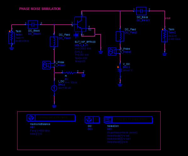
70 EXAMPLE 5: NOISE PARAMETERS AND 1/F NOISE The graphics below show sample schematics for performing a noise parameter and phase noise simulations. The noise parameter simulation is set up for a bias condition of 2V and 20 ma and a frequency range of 2 to 6 GHz. The phase noise simulation is set up for a bias condition of 2V and 10 ma. The bias set up uses a current source on the input and a voltage source on the output. 70 of 100
71 NFmin Simulation results for the schematic set up for noise parameter simulation over a frequency range from 2 to 6 GHz. The markers correspond to measurement data points Rn Frequency (GHz) 5 Gamma_opt 71 of 100
72 72 of 100
73 1/f noise (dba/hz) Simulation results for the schematic set up for 1/f noise simulation over a frequency range from 1 to 0.1 MHz. The markers correspond to measurement data points E1 1E2 1E3 1E4 1E5 Frequency (Hz) 73 of 100


74 EXAMPLE 6: TWO-TONE INTERMODULATION SIMULATION The graphic below shows a sample schematic for performing a two-tone intermodulation simulation to determine the intermodulation products of the third order when subjected to two signals with 1 MHZ frequency spacing. The model is set for simulation at a nominal bias voltage of 3V and 60 ma on a 14 mil thick FR4 substrate. The source and the load impedances are set to 50 ohms and 93+j42 ohms, respectively. 74 of 100
75 Pout (dbm) Simulation results for the schematic set up for simulation when two signals with 1 MHz frequency spacing are applied. The markers correspond to measurement data points Carrier rd order product Pin (dbm) 75 of 100

76 EXAMPLE 7: LOAD PULL SIMULATIONS The graphic below shows a sample schematic for performing a load pull simulation for a BJT model. The model is set up for simulation at an input frequency of 0.9 GHz and input power of -2 dbm on 14 mil FR4 substrate at VCE=5V and IC=8 ma. The source impedance is set to 50 ohms. 76 of 100
77 Simulation results for the schematic set up for load simulation at an input frequency of 0.9GHz and input power of -2 dbm. Pout (dbm) ZL PAE, % ZL Measured /35.25 deg /34.09 Model / /42.24 Maximum Power-Added Efficiency, % Maximum Power Delivered, dbm of 100
78 ADDITIONAL NLT EXAMPLES Additional examples are included in the library. All examples are available in both project and workspace format and can be found in the <InstallDir>\Library\MDLX_NLT_dk_Library\examples folder where <InstallDir> is the installation folder selected during installation (default is C:\Modelithics). MDLX_NLT_Datasheet_examples_prj(wrk) These examples can be used to verify the model performance matches the documented results. Schematic Biased_Spar_Ib DCIV_with_Base_Current DCIV_with_Base_Voltage Gain_Compression HB1Tone_Pswp Noise_Parameters S_Parameters Description Sub-circuit model for the Noise_Parameters example. This circuit uses the BJT-NEC-NE85633 model A DC I-V curve setup with a current source applied to the base of the BJT-AGT-AT64023 model. A DC I-V curve setup with a voltage source applied at the gate of the MES-EXC-EFA060BS5 model. This example shows a typical gain compression setup using the BJT-NEC-NE85633 model. This example is a Harmonic Balance simulation of the BJT-NEC-NE85633 model. A noise parameter example using the Biased_Spar_Ib sub-circuit. An S-Parameter example schematic for the HMT-AGT- ATF511P8 model. 78 of 100


79 SLC EXAMPLES EXAMPLE 1: MIXER CL COMPRESS TEST The following schematic shows a typical setup using the MIX_MAX_2681_001 model to predict the conversion gain/loss performance of the mixer with respect to swept LO power levels. The mixer model accepts two input parameters, RFfreq and LOfreq referring to the input RF frequency and LO frequency. As will be shown in the simulated figure, the mixer presents an increasing conversion gain vs. ascending LO power levels. 79 of 100
80 Simulation results for the mixer CL compression test schematic. 80 of 100
.")

 for matched conditions.")
81 EXAMPLE 2: AMPLIFIER POWER SWEEP SIMULATION This schematic is used for predicting the gain compression results for the MAXIM2371 Amplifier at a specified frequency (Freq). The 2371 model as two inputs: SimOption and Input Frequency. Setting the SimOption=0; InputFrequency = Freq invokes the Harmonic balance power simulation. The source and the load impedances can be set to 50 ohms or the corresponding source and the load impedances at three specific frequencies (136, 155 and 174 MHz) for matched conditions. When using s-parameter simulator, InputFrequency should be set to freq for the sweeping frequency value. 81 of 100
82 Simulation results for the power sweep schematic. 82 of 100


83 EXAMPLE 3: AMPLIFIER S-PARAMETER SIMULATION This schematic is used for predicting the small signal S-parameter results for the MAXIM2373 Amplifier over a frequency range from 0.04 through 2.5GHz. The 2373 model has two inputs: SimOption and InputFrequency. Setting the SimOption=1; InputFrequency= freq invokes the S-parameter simulation. When using the Harmonic balance, power and load-pull simulator, SimOption should be set to 0 and InputFrequency shod be set to Freq for the corresponding fixed frequency value. 83 of 100
84 Simulation results for the S-parameter schematic. 84 of 100

85 EXAMPLE 4: COUPLER TRANSIENT SIMULATION Following example schematic demonstrates how to setup the transient simulation using the AVX CP0603 coupler. The substrate information is accepted to provide the substratescalability. The simulation result shown in the following presents the relationship between the input and the coupled ports, both the magnitude and the phase variation. 85 of 100
86 Simulation results for the transient schematic. 86 of 100


87 EXAMPLE 5: RFMD AMPLIFIER BEHAVIORAL SIMULATION Following example schematic demonstrates the typical simulation setup using the RFMD RF2132 amplifier model. One can choose to simulate the S-parameter or large-signal power compression performance by enabling different stimulating sources, as shown in the following figure. 87 of 100
88 Simulation results for the amplifier behavioral schematic. S-Parameters Power Sweep Results 88 of 100

89 Spectrum (dbm) EXAMPLE 6: X-PARAMETER MODEL SIMULATION Several X-parameter models are included in the library. Here shows an example setup on how to use the RFMD RF2878 X-parameter model in HB simulation. There is an application note on the model's performance ( One can also find out more about the model in the example project in the library (AMPXP-RFMD-RF2878_example_paper_version_prj) RFpow er 89 of 100
90 ADDITIONAL SLC EXAMPLES Additional examples are included in the library. All examples are available in both project and workspace format and can be found in the <InstallDir>\Library\MDLX_SLC_dk_Library\examples folder where <InstallDir> is the installation folder selected during installation (default is C:\Modelithics). AMP_RFMD_RF2878_001_prj(wrk) Examples in this project are for the RFMD RF2878 Amplifier X-Parameter model. Schematic ENV_2TonePswp_XP HB_1Tone_Loadpull_XP Description An example schematic for TOI. An example schematic for simulating loadpull contours under 1-tone simuli. HB_1Tone_pswp_XP An example schematic for simulating power compression performance. SLC_Example_prj(wrk) Examples of various component models in the SLC library. Schematic Description Datasheet_BEH_S2D_HB_1tone_Report A 1 tone harmonic balance simulation using the AMP-NEC-UPC8179TK-001 model. Datasheet_Noise_parameter This example reproduces the Mode Noise Data plot of the AMP-TRI-TGA8399B-001 model. S_parm_BPF_TOYO_HFF101B_001 An S-Parameter setup for the band-pass filter model BPF-TOYO-HFF101B-001. Sparm_DPX_SAW_856331_001 A 3-port S-Parameter setup for the DPX-SAW duplexer model. Sparm_RSN_MUR_1200_001 This S-Parameter example shows the substrate scaling of the resonator model RSN-MUR Sparm_SWT_MAC_MASWSS0204_001 The SWT-MAC-MASWSS switch model is configured to run S-parameters. 90 of 100
 DC BIAS This example demonstrates the")

91 SELECT EXAMPLES EXAMPLE 1: DUAL GATE MOSFET (BF1211) DC BIAS This example demonstrates the DC bias conditions of the dual gate BF1211 model and compares the results to measurement data. 91 of 100
92 Id (A) Simulation results for the bias condition of Vds=0 to 6V, Vgs2=4v, and various values of Vgs1. The model performance is show by the solid red lines and the measured data is shown by the blue circles Vds (V) Vg1=1.500 Vg1=1.400 Vg1=1.300 Vg1=1.200 Vg1=1.100 Vg1=1.000 Vg1=0.900 Vg1= of 100


93 EXAMPLE 2: DUAL GATE MOSFET (BF1212) 1DB COMPRESSION POINT The graphic below shows a sample schematic for performing a 1dB compression point simulation for the DGMOS_PHL_BF1212 model. The model results are then compared to measured results. 93 of 100
94 Gain (db) real(i_probe1.i[::,0]) Simulation results for the BF1212 model vs measured data. m2 RFpower= real(i_probe1.i[::,0])= m RFpower Pin (dbm) Pout (dbm) 94 of 100

95 EXAMPLE 3: ACTIVE DEVICE YIELD ANALYSIS EXAMPLE This example demonstrates a yield analysis using the SKD_INF_ST23001 Infineon BAS40 Schottky diode model. A statistical variation of bias condition is performed using Monte Carlo analysis. 95 of 100
96 S21 (db) S11 (db) Simulation results for the yield analysis Frequency (GHz) Frequency (GHz) 96 of 100

97 EXAMPLE 4: DC I-V, S-PARAMETERS AND FLICKER NOISE SIMULATION WITH HBT- NEC-NESG S This example demonstrates a DC I-V, S-parameter and 1/f noise simulation with the HBT- NEC-NESG S. 97 of 100
98 Simulation results. 98 of 100

99 EXAMPLE 5: LTCC FILTER SIMULATION USING DIFFERENT SUBSTRATE PROPERTIES The graphic below shows a sample schematic for performing a surface mount LTCC filter simulation using different substrate properties for a model. The model is set for simulation on 5, 14, and 59 mil thick FR4 substrates. For all substrates, the pad stack conductor thickness is mm. 99 of 100
100 Simulation Results: 100 of 100
, 现已发展成为国内最大的微波射频和天线设计人才培养基地, 成功推出多套微波射频以及天线设计经典培训课程和 ADS HFSS 等专业软件使用培训课程, 广受客户好评 ; 并先后与人民邮电出版社 电子工业出版社合作出版了多本专业图书, 帮助数万名工程师提升了专业技术能力 客户遍布中兴通讯 研通高频 埃威航电 国人通信等多家国内知名公司, 以及台湾工业技术研究院")


101 易迪拓培训 专注于微波 射频 天线设计人才的培养网址 : 射频和天线设计培训课程推荐 易迪拓培训 ( 由数名来自于研发第一线的资深工程师发起成立, 致力并专注于微波 射频 天线设计研发人才的培养 ; 我们于 2006 年整合合并微波 EDA 网 ( 现已发展成为国内最大的微波射频和天线设计人才培养基地, 成功推出多套微波射频以及天线设计经典培训课程和 ADS HFSS 等专业软件使用培训课程, 广受客户好评 ; 并先后与人民邮电出版社 电子工业出版社合作出版了多本专业图书, 帮助数万名工程师提升了专业技术能力 客户遍布中兴通讯 研通高频 埃威航电 国人通信等多家国内知名公司, 以及台湾工业技术研究院 永业科技 全一电子等多家台湾地区企业 易迪拓培训课程列表 : 射频工程师养成培训课程套装该套装精选了射频专业基础培训课程 射频仿真设计培训课程和射频电路测量培训课程三个类别共 30 门视频培训课程和 3 本图书教材 ; 旨在引领学员全面学习一个射频工程师需要熟悉 理解和掌握的专业知识和研发设计能力 通过套装的学习, 能够让学员完全达到和胜任一个合格的射频工程师的要求 课程网址 : ADS 学习培训课程套装该套装是迄今国内最全面 最权威的 ADS 培训教程, 共包含 10 门 ADS 学习培训课程 课程是由具有多年 ADS 使用经验的微波射频与通信系统设计领域资深专家讲解, 并多结合设计实例, 由浅入深 详细而又全面地讲解了 ADS 在微波射频电路设计 通信系统设计和电磁仿真设计方面的内容 能让您在最短的时间内学会使用 ADS, 迅速提升个人技术能力, 把 ADS 真正应用到实际研发工作中去, 成为 ADS 设计专家... 课程网址 : HFSS 学习培训课程套装该套课程套装包含了本站全部 HFSS 培训课程, 是迄今国内最全面 最专业的 HFSS 培训教程套装, 可以帮助您从零开始, 全面深入学习 HFSS 的各项功能和在多个方面的工程应用 购买套装, 更可超值赠送 3 个月免费学习答疑, 随时解答您学习过程中遇到的棘手问题, 让您的 HFSS 学习更加轻松顺畅 课程网址 : `

102 易迪拓培训 专注于微波 射频 天线设计人才的培养网址 : CST 学习培训课程套装该培训套装由易迪拓培训联合微波 EDA 网共同推出, 是最全面 系统 专业的 CST 微波工作室培训课程套装, 所有课程都由经验丰富的专家授课, 视频教学, 可以帮助您从零开始, 全面系统地学习 CST 微波工作的各项功能及其在微波射频 天线设计等领域的设计应用 且购买该套装, 还可超值赠送 3 个月免费学习答疑 课程网址 : HFSS 天线设计培训课程套装套装包含 6 门视频课程和 1 本图书, 课程从基础讲起, 内容由浅入深, 理论介绍和实际操作讲解相结合, 全面系统的讲解了 HFSS 天线设计的全过程 是国内最全面 最专业的 HFSS 天线设计课程, 可以帮助您快速学习掌握如何使用 HFSS 设计天线, 让天线设计不再难 课程网址 : MHz NFC/RFID 线圈天线设计培训课程套装套装包含 4 门视频培训课程, 培训将 13.56MHz 线圈天线设计原理和仿真设计实践相结合, 全面系统地讲解了 13.56MHz 线圈天线的工作原理 设计方法 设计考量以及使用 HFSS 和 CST 仿真分析线圈天线的具体操作, 同时还介绍了 13.56MHz 线圈天线匹配电路的设计和调试 通过该套课程的学习, 可以帮助您快速学习掌握 13.56MHz 线圈天线及其匹配电路的原理 设计和调试 详情浏览 : 我们的课程优势 : 成立于 2004 年,10 多年丰富的行业经验, 一直致力并专注于微波射频和天线设计工程师的培养, 更了解该行业对人才的要求 经验丰富的一线资深工程师讲授, 结合实际工程案例, 直观 实用 易学 联系我们 : 易迪拓培训官网 : 微波 EDA 网 : 官方淘宝店 : 专注于微波 射频 天线设计人才的培养易迪拓培训官方网址 : 淘宝网店 :
surface mount chip capacitor model
 S (db) CAP-PPI-78N- surface mount chip capacitor model Model Features* Broadband validation: DC 4 GHz Equivalent circuit based Substrate scalable:(.9 H/Er 6.5 mil) Part value scalable: (. to pf) Land Pattern
surface mount chip capacitor model
 surface mount chip capacitor model Model Features* Broadband validation: DC 30 GHz Equivalent circuit based Applicable for horizontal mounted capacitors Substrate scalable: (1 H/Er 16.7 mil) Part value
surface mount chip ferrite bead model
 surface mount chip ferrite bead model Model Features Broadband (DC to 6GHz) Equivalent circuit based Substrate scalable (1. H/Er 16.4) Part value selectable: rated 1 to 18 ohms Bias Sensing Capability:
Original Procedure by University of South Florida, Modified by Baylor University.
 1 ELC 4384 RF/Microwave Circuits II Spring 2018 Final Design Project: Design, Simulation, and Testing of a Low-Noise Amplifier Due Thursday, April 26, 12:30 p.m. Note: This procedure has been adapted from
2005 Modelithics Inc.
 Precision Measurements and Models You Trust Modelithics, Inc. Solutions for RF Board and Module Designers Introduction Modelithics delivers products and services to serve one goal accelerating RF/microwave
Substrate Libraries Ease PCB Simulations
 1 of 6 3/25/2013 10:38 PM print close Substrate Libraries Ease PCB Simulations Scott Muir, Eric O'Dell, Laura Levesque, Hugo Morales, and Larry Dunleavy Tue, 2013-02-26 14:13 These measurement-based substrate
Advanced Design in Keysight. Genesys with Modelithics Models
 Advanced Design in Keysight Genesys with Modelithics Models 1 What We ll Cover: What is the Modelithics COMPLETE Library? What are the key specialized features of Modelithics models for accurate simulation
Evaluation of Package Properties for RF BJTs
 Application Note Evaluation of Package Properties for RF BJTs Overview EDA simulation software streamlines the development of digital and analog circuits from definition of concept and estimation of required
Application Note 1131
 Low Noise Amplifiers for 320 MHz and 850 MHz Using the AT-32063 Dual Transistor Application Note 1131 Introduction This application note discusses the Avago Technologies AT-32063 dual low noise silicon
Application Note 5012
 MGA-61563 High Performance GaAs MMIC Amplifier Application Note 5012 Application Information The MGA-61563 is a high performance GaAs MMIC amplifier fabricated with Avago Technologies E-pHEMT process and
Application Note 5011
 MGA-62563 High Performance GaAs MMIC Amplifier Application Note 511 Application Information The MGA-62563 is a high performance GaAs MMIC amplifier fabricated with Avago Technologies E-pHEMT process and
Leveraging High-Accuracy Models to Achieve First Pass Success in Power Amplifier Design
 Application Note Leveraging High-Accuracy Models to Achieve First Pass Success in Power Amplifier Design Overview Nonlinear transistor models enable designers to concurrently optimize gain, power, efficiency,
Application Note 5525
 Using the Wafer Scale Packaged Detector in 2 to 6 GHz Applications Application Note 5525 Introduction The is a broadband directional coupler with integrated temperature compensated detector designed for
Using Accurate Component Models to Achieve First-Pass Success in Filter Design
 Application Example Using Accurate Component Models to Achieve First-Pass Success in Filter Design Overview Utilizing models that include component and printed circuit board (PCB) parasitics in place of
Application Note 5057
 A 1 MHz to MHz Low Noise Feedback Amplifier using ATF-4143 Application Note 7 Introduction In the last few years the leading technology in the area of low noise amplifier design has been gallium arsenide
Accurate Simulation of RF Designs Requires Consistent Modeling Techniques
 From September 2002 High Frequency Electronics Copyright 2002, Summit Technical Media, LLC Accurate Simulation of RF Designs Requires Consistent Modeling Techniques By V. Cojocaru, TDK Electronics Ireland
Maxim > Design Support > Technical Documents > Application Notes > Wireless and RF > APP 3571
 Maxim > Design Support > Technical Documents > Application Notes > Wireless and RF > APP 3571 Keywords: automotive keyless entry, MAX2640, LNA, 315MHz, RKE, stability, automotive, keyless entry APPLICATION
Application Note 5446
 Design the Avago MGA-31T6 into a High Gain, Low Noise, Low current GPS LNA Module Application Note 446 Introduction The MGA-31T6 is a low cost and easy-to-use GaAs LNA (Low Noise Amplifier). The LNA is
Low Noise Amplifier for 3.5 GHz using the Avago ATF Low Noise PHEMT. Application Note 1271
 Low Noise Amplifier for 3. GHz using the Avago ATF-3143 Low Noise PHEMT Application Note 171 Introduction This application note describes a low noise amplifier for use in the 3.4 GHz to 3.8 GHz wireless
Application Note 1285
 Low Noise Amplifiers for 5.125-5.325 GHz and 5.725-5.825 GHz Using the ATF-55143 Low Noise PHEMT Application Note 1285 Description This application note describes two low noise amplifiers for use in the
RF/Microwave Circuits I. Introduction Fall 2003
 Introduction Fall 03 Outline Trends for Microwave Designers The Role of Passive Circuits in RF/Microwave Design Examples of Some Passive Circuits Software Laboratory Assignments Grading Trends for Microwave
This article describes the design of a multiband,
 A Low-Noise Amplifier for 2 GHz Applications Using the NE334S01 Transistor By Ulrich Delpy NEC Electronics (Europe) This article describes the design of a multiband, low-noise amplifier (LNA) using the
Dr.-Ing. Ulrich L. Rohde
 Dr.-Ing. Ulrich L. Rohde Noise in Oscillators with Active Inductors Presented to the Faculty 3 : Mechanical engineering, Electrical engineering and industrial engineering, Brandenburg University of Technology
ATF-531P8 900 MHz High Linearity Amplifier. Application Note 1372
 ATF-531P8 9 MHz High Linearity Amplifier Application Note 1372 Introduction This application note describes the design and construction of a single stage 85 MHz to 9 MHz High Linearity Amplifier using
ATF High Intercept Low Noise Amplifier for the MHz PCS Band using the Enhancement Mode PHEMT
 ATF-54143 High Intercept Low Noise Amplifier for the 185 191 MHz PCS Band using the Enhancement Mode PHEMT Application Note 1222 Introduction Avago Technologies ATF-54143 is a low noise enhancement mode
A 400, 900, and 1800 MHz Buffer/Driver Amplifier using the HBFP-0450 Silicon Bipolar Transistor
 A 4, 9, and 18 MHz Buffer/Driver Amplifier using the HBFP-4 Silicon Bipolar Transistor Application Note 16 Introduction Avago Technologies HBFP-4 is a high performance isolated collector silicon bipolar
1 of 7 12/20/ :04 PM
 1 of 7 12/20/2007 11:04 PM Trusted Resource for the Working RF Engineer [ C o m p o n e n t s ] Build An E-pHEMT Low-Noise Amplifier Although often associated with power amplifiers, E-pHEMT devices are
RF2418 LOW CURRENT LNA/MIXER
 LOW CURRENT LNA/MIXER RoHS Compliant & Pb-Free Product Package Style: SOIC-14 Features Single 3V to 6.V Power Supply High Dynamic Range Low Current Drain High LO Isolation LNA Power Down Mode for Large
RF2044A GENERAL PURPOSE AMPLIFIER
 GENERAL PURPOSE AMPLIFIER RoHS Compliant and Pb-Free Product Package Style: Micro-X Ceramic Features DC to >6000MHz Operation Internally matched Input and Output 18.5dB Small Signal Gain @ 2GHz 4.0dB Noise
400 MHz to 4000 MHz ½ Watt RF Driver Amplifier ADL5324
 Data Sheet FEATURES Operation from MHz to MHz Gain of 14.6 db at 21 MHz OIP of 4.1 dbm at 21 MHz P1dB of 29.1 dbm at 21 MHz Noise figure of.8 db Dynamically adjustable bias Adjustable power supply bias:.
Application Note 5460
 MGA-89 High Linearity Amplifier with Low Operating Current for 9 MHz to. GHz Applications Application Note 6 Introduction The Avago MGA-89 is a high dynamic range amplifier designed for applications in
Application Note 5499
 MGA-31389 and MGA-31489 High-Gain Driver Amplifier Using Avago MGA-31389 and MGA-31489 Application Note 5499 Introduction The MGA-31389 and MGA-31489 from Avago Technologies are.1 Watt flat-gain driver
APPLICATION NOTE 052. A Design Flow for Rapid and Accurate Filter Prototyping
 APPLICATION NOTE 052 A Design Flow for Rapid and Accurate Filter Prototyping Introduction Filter designers for RF/microwave requirements are challenged with meeting an often-conflicting set of performance
CHAPTER 4. Practical Design
 CHAPTER 4 Practical Design The results in Chapter 3 indicate that the 2-D CCS TL can be used to synthesize a wider range of characteristic impedance, flatten propagation characteristics, and place passive
A Colpitts VCO for Wideband ( GHz) Set-Top TV Tuner Applications
 Set-Top TV Tuner Applications") A Colpitts VCO for Wideband (0.95 2.15 GHz) Set-Top TV Tuner Applications Application Note Introduction Modern set-top DBS TV tuners require high performance, broadband voltage control oscillator (VCO)
A Colpitts VCO for Wideband (0.95 2.15 GHz) Set-Top TV Tuner Applications Application Note Introduction Modern set-top DBS TV tuners require high performance, broadband voltage control oscillator (VCO)
Application Note 5482
 MGA-31189 70 to 500 MHz Amplifier for IF Applications using the Avago Technologies MGA-31189 Amplifier Application Note 5482 Introduction The MGA-31189 is a highly linear, Enhancement mode phemt (Pseudomorphic
800 to 950 MHz Amplifiers using the HBFP-0405 and HBFP-0420 Low Noise Silicon Bipolar Transistors. Application Note 1161
 8 to 95 MHz Amplifiers using the HBFP-45 and HBFP-42 Low Noise Silicon Bipolar Transistors Application Note 1161 Introduction Hewlett-Packard s HBFP-45 and HBFP-42 are high performance isolated collector
Application Note 1299
 A Low Noise High Intercept Point Amplifier for 9 MHz Applications using ATF-54143 PHEMT Application Note 1299 1. Introduction The Avago Technologies ATF-54143 is a low noise enhancement mode PHEMT designed
MGA GHz 3 V, 17 dbm Amplifier. Data Sheet. Features. Description. Applications. Surface Mount Package. Simplified Schematic
 MGA-853.1 GHz 3 V, 17 dbm Amplifier Data Sheet Description Avago s MGA-853 is an economical, easy-to-use GaAs MMIC amplifier that offers excellent power and low noise figure for applications from.1 to
Discrete Circuit Design
 Design Feature CHRIS DeMARTINO Technical Engineering Editor Take the Guesswork Out of Discrete Circuit Design A new software tool enables engineers to efficiently design circuits with models of actual
ATF-531P8 E-pHEMT GaAs FET Low Noise Amplifier Design for 800 and 900 MHz Applications. Application Note 1371
 ATF-31P8 E-pHEMT GaAs FET Low Noise Amplifier Design for 8 and 9 MHz Applications Application Note 1371 Introduction A critical first step in any LNA design is the selection of the active device. Low cost
UM User manual for the BGU7004 GPS LNA evaluation board. Document information. Keywords LNA, GPS, BGU7004. Abstract
 User manual for the BGU7004 GPS LNA evaluation board Rev. 1.0 14 June 2011 User manual Document information Info Keywords Abstract Content LNA, GPS, BGU7004 This document explains the BGU7004 AEC-Q100
Data Sheet. MGA GHz 3 V, 14 dbm Amplifier. Description. Features. Applications. Simplified Schematic
 MGA-8153.1 GHz 3 V, 1 dbm Amplifier Data Sheet Description Avago s MGA-8153 is an economical, easy-to-use GaAs MMIC amplifier that offers excellent power and low noise figure for applications from.1 to
RF3375 GENERAL PURPOSE AMPLIFIER
 Basestation Applications Broadband, Low-Noise Gain Blocks IF or RF Buffer Amplifiers Driver Stage for Power Amplifiers Final PA for Low-Power Applications High Reliability Applications RF3375General Purpose
Application Note 1330
 HMPP-3865 MiniPAK PIN Diode High Isolation SPDT Switch Design for 1.9 GHz and 2.45 GHz Applications Application Note 133 Introduction The Avago Technologies HMPP-3865 parallel diode pair combines low inductance,
Application Note 5468
 GA-43228 High Linearity Wireless Data Power Amplifier for 2.3 to 2.5 GHz Applications Application Note 5468 Introduction This application note describes the GA-43228 power amplifier and gives actual performance
Application Note 1360
 ADA-4743 +17 dbm P1dB Avago Darlington Amplifier Application Note 1360 Description Avago Technologies Darlington Amplifier, ADA-4743 is a low current silicon gain block RFIC amplifier housed in a 4-lead
RF2044 GENERAL PURPOSE AMPLIFIER
 GENERAL PURPOSE AMPLIFIER RoHS Compliant & Pb-Free Product Package Style: Micro-X Ceramic Features DC to >6000MHz Operation Internally matched Input and Output 20dB Small Signal Gain 4.0dB Noise Figure
Innovations in EDA Webcast Series
 Welcome Innovations in EDA Webcast Series August 2, 2012 Jack Sifri MMIC Design Flow Specialist IC, Laminate, Package Multi-Technology PA Module Design Methodology Realizing the Multi-Technology Vision
77 GHz VCO for Car Radar Systems T625_VCO2_W Preliminary Data Sheet
 77 GHz VCO for Car Radar Systems Preliminary Data Sheet Operating Frequency: 76-77 GHz Tuning Range > 1 GHz Output matched to 50 Ω Application in Car Radar Systems ESD: Electrostatic discharge sensitive
RF Board Design for Next Generation Wireless Systems
 RF Board Design for Next Generation Wireless Systems Page 1 Introduction Purpose: Provide basic background on emerging WiMax standard Introduce a new tool for Genesys that will aide in the design and verification
RF Circuit Synthesis for Physical Wireless Design
 RF Circuit Synthesis for Physical Wireless Design Overview Subjects Review Of Common Design Tasks Break Down And Dissect Design Task Review Non-Synthesis Methods Show A Better Way To Solve Complex Design
MAX1002/MAX1003 Evaluation Kits
 9-50; Rev 0; 6/97 MAX00/MAX00 Evaluation Kits General Description The MAX00/MAX00 evaluation kits (EV kits) simplify evaluation of the 60Msps MAX00 and 90Msps MAX00 dual, 6-bit analog-to-digital converters
Demo Circuit DC550A Quick Start Guide.
 May 12, 2004 Demo Circuit DC550A. Introduction Demo circuit DC550A demonstrates operation of the LT5514 IC, a DC-850MHz bandwidth open loop transconductance amplifier with high impedance open collector
Product Description. Ordering Information. GaAs HBT GaAs MESFET InGaP HBT
 Basestation pplications Broadband, Low-Noise Gain Blocks IF or RF Buffer mplifiers Driver Stage for Power mplifiers Final P for Low-Power pplications High Reliability pplications RF3396General Purpose
87x. MGA GHz 3 V Low Current GaAs MMIC LNA. Data Sheet
 MGA-876 GHz V Low Current GaAs MMIC LNA Data Sheet Description Avago s MGA-876 is an economical, easy-to-use GaAs MMIC amplifier that offers low noise and excellent gain for applications from to GHz. Packaged
Application Note No. 075
 Application Note, Rev. 2.0, Jan. 2007 Application Note No. 075 High Third-Order Input Intercept Point CDMA 800 Low Noise Amplifier RF & Protection Devices Edition 2007-01-08 Published by Infineon Technologies
PART MAX2605EUT-T MAX2606EUT-T MAX2607EUT-T MAX2608EUT-T MAX2609EUT-T TOP VIEW IND GND. Maxim Integrated Products 1
 19-1673; Rev 0a; 4/02 EVALUATION KIT MANUAL AVAILABLE 45MHz to 650MHz, Integrated IF General Description The are compact, high-performance intermediate-frequency (IF) voltage-controlled oscillators (VCOs)
MGA GHz 3 V, 17 dbm Amplifier. Data Sheet
 MGA-853.1 GHz 3 V, 17 dbm Amplifier Data Sheet Description Avago s MGA-853 is an economical, easy-to-use GaAs MMIC amplifier that offers excellent power and low noise figure for applications from.1 to
Schottky diode mixer for 5.8 GHz radar sensor
 AN_1808_PL32_1809_130625 Schottky diode mixer for 5.8 GHz radar sensor About this document Scope and purpose This application note shows a single balanced mixer for 5.8 GHz Doppler radar applications with
Including the proper parasitics in a nonlinear
 Effects of Parasitics in Circuit Simulations Simulation accuracy can be improved by including parasitic inductances and capacitances By Robin Croston California Eastern Laboratories Including the proper
83x. Data Sheet. MGA dbm P SAT 3 V Power Amplifier for GHz Applications. Description. Features. Applications
 MGA-83563 +22 dbm P SAT 3 V Power Amplifier for 0.5 6 GHz Applications Data Sheet Description Avago s MGA-83563 is an easy-to-use GaAs IC amplifier that offers excellent power output and efficiency. This
20 MHz to 6 GHz RF/IF Gain Block ADL5542
 FEATURES Fixed gain of db Operation up to 6 GHz Input/output internally matched to Ω Integrated bias control circuit Output IP3 46 dbm at MHz 4 dbm at 9 MHz Output 1 db compression:.6 db at 9 MHz Noise
SZM-3066Z. 3.3GHz to 3.8GHz 2W POWER AMPLIFIER. Product Description. Features. Applications. Package: QFN, 6mmx6mm
 3.3GHz to 3.8GHz 2W Power Amplifier SZM-3066Z 3.3GHz to 3.8GHz 2W POWER AMPLIFIER Package: QFN, 6mmx6mm Product Description RFMD s SZM-3066Z is a high linearity class AB Heterojunction Bipolar Transistor
High IP3 Low-Noise Amplifier
 EVALUATION KIT AVAILABLE General Description The low-cost, high third-order intercept point (IP3) low-noise amplifier (LNA) is designed for applications in 2.4GHz WLAN, ISM, and Bluetooth radio systems.
VCC GND RF IN. Product Description. Ordering Information. GaAs HBT GaAs MESFET InGaP HBT
 .GHz Low Noise Amplifier with Enable RF7G.GHz LOW NOISE AMPLIFIER WITH ENABLE Package Style: SOT Lead Features DC to >6GHz Operation.7V to.0v Single Supply High Input IP.dB Noise Figure at 00MHz db Gain
Maxim Integrated Products 1
 19-3533; Rev 0; 1/05 MAX9996 Evaluation Kit General Description The MAX9996 evaluation kit (EV kit) simplifies the evaluation of the MAX9996 UMTS, DCS, and PCS base-station downconversion mixer. It is
Keywords: rf, rfic, wireless, cellular, cdma, if, oscillator, rfics, IF frequencies, VCO, rf ic
 Maxim > Design Support > Technical Documents > Application Notes > Wireless and RF > APP 272 Keywords: rf, rfic, wireless, cellular, cdma, if, oscillator, rfics, IF frequencies, VCO, rf ic APPLICATION
Maxim Integrated Products 1
 19-0569; Rev 0; 5/06 MAX2041 Evaluation Kit General Description The MAX2041 evaluation kit (EV kit) simplifies the evaluation of the MAX2041 UMTS, DCS, and PCS base-station up/downconversion mixer. It
Methodology for MMIC Layout Design
 17 Methodology for MMIC Layout Design Fatima Salete Correra 1 and Eduardo Amato Tolezani 2, 1 Laboratório de Microeletrônica da USP, Av. Prof. Luciano Gualberto, tr. 3, n.158, CEP 05508-970, São Paulo,
Data Sheet. MGA-632P8 Low Noise, High Linearity Active Bias Low Noise Amplifier. Features. Description. Specifications.
 MGA-632P8 Low Noise, High Linearity Active Bias Low Noise Amplifier Data Sheet Description Avago Technologies MGA-632P8 is an economical, easyto-use GaAs MMIC Low Noise Amplifier (LNA) with active bias.
DESIGNATION QTY DESCRIPTION
 19-2686; Rev 1; 2/04 MAX2027 Evaluation Kit General Description The MAX2027 evaluation kit (EV kit) simplifies the evaluation of the MAX2027 high-linearity, digitally controlled, variable-gain amplifier.
When Should You Apply 3D Planar EM Simulation?
 When Should You Apply 3D Planar EM Simulation? Agilent EEsof EDA IMS 2010 MicroApps Andy Howard Agilent Technologies 1 3D planar EM is now much more of a design tool Solves bigger problems and runs faster
Large-Signal S-Parameter Simulation
 Large-Signal S-Parameter Simulation May 2003 Notice The information contained in this document is subject to change without notice. Agilent Technologies makes no warranty of any kind with regard to this
MGA-725M4 Low Noise Amplifier with Bypass Switch In Miniature Leadless Package. Data Sheet. Description. Features. Applications
 MGA-75M Low Noise Amplifier with Bypass Switch In Miniature Leadless Package Data Sheet Description Broadcom's MGA -75M is an economical, easy-to-use GaAs MMIC Low Noise Amplifier (LNA), which is designed
20 GHz to 44 GHz, GaAs, phemt, MMIC, Low Noise Amplifier HMC1040CHIPS
 Data Sheet FEATURES Low noise figure: 2 db typical High gain: 25. db typical P1dB output power: 13.5 dbm, 2 GHz to GHz High output IP3: 25.5 dbm typical Die size: 1.39 mm 1..2 mm APPLICATIONS Software
400 MHz 4000 MHz Low Noise Amplifier ADL5521
 FEATURES Operation from 400 MHz to 4000 MHz Noise figure of 0.8 db at 900 MHz Including external input match Gain of 20.0 db at 900 MHz OIP3 of 37.7 dbm at 900 MHz P1dB of 22.0 dbm at 900 MHz Integrated
Surface Mount SOT-363 (SC-70) Package. Pin Connections and Package Marking GND. V dd. Note: Package marking provides orientation and identification.
 Package. Pin Connections and Package Marking GND. V dd. Note: Package marking provides orientation and identification.") GHz V Low Current GaAs MMIC LNA Technical Data MGA-876 Features Ultra-Miniature Package.6 db Min. Noise Figure at. GHz. db Gain at. GHz Single + V or V Supply,. ma Current Applications LNA or Gain Stage
GHz V Low Current GaAs MMIC LNA Technical Data MGA-876 Features Ultra-Miniature Package.6 db Min. Noise Figure at. GHz. db Gain at. GHz Single + V or V Supply,. ma Current Applications LNA or Gain Stage
ABA GHz Broadband Silicon RFIC Amplifier. Application Note 1349
 ABA-52563 3.5 GHz Broadband Silicon RFIC Amplifier Application Note 1349 Introduction Avago Technologies ABA-52563 is a low current silicon gain block RFIC amplifier housed in a 6-lead SC 70 (SOT- 363)
Figure Main frame of IMNLab.
 IMNLab Tutorial This Tutorial guides the user to go through the design procedure of a wideband impedance match network for a real circuit by using IMNLab. Wideband gain block TQP3M97 evaluation kit from
Application Note 5480
 ALM-2712 Ultra Low-Noise GPS Amplifier with Pre- and Post-Filter Application Note 548 Introduction The ALM-2712 is a GPS front-end module which consists of a low noise amplifier with pre- and post-filters.
SP 22.3: A 12mW Wide Dynamic Range CMOS Front-End for a Portable GPS Receiver
 SP 22.3: A 12mW Wide Dynamic Range CMOS Front-End for a Portable GPS Receiver Arvin R. Shahani, Derek K. Shaeffer, Thomas H. Lee Stanford University, Stanford, CA At submicron channel lengths, CMOS is
ECEN 5014, Spring 2009 Special Topics: Active Microwave Circuits Zoya Popovic, University of Colorado, Boulder
 ECEN 5014, Spring 2009 Special Topics: Active Microwave Circuits Zoya opovic, University of Colorado, Boulder LECTURE 3 MICROWAVE AMLIFIERS: INTRODUCTION L3.1. TRANSISTORS AS BILATERAL MULTIORTS Transistor
Large-Signal S-Parameter Simulation
 Large-Signal S-Parameter Simulation September 2004 Notice The information contained in this document is subject to change without notice. Agilent Technologies makes no warranty of any kind with regard
DESCRIPTIO FEATURES APPLICATIO S. LT GHz to 2.7GHz Receiver Front End TYPICAL APPLICATIO
 1.GHz to 2.GHz Receiver Front End FEATURES 1.V to 5.25V Supply Dual LNA Gain Setting: +13.5dB/ db at Double-Balanced Mixer Internal LO Buffer LNA Input Internally Matched Low Supply Current: 23mA Low Shutdown
CGA-6618Z Dual CATV 5MHz to 1000MHz High Linearity GaAs HBT Amplifier CGA-6618Z DUAL CATV 5MHz to 1000MHz HIGH LINEARITY GaAs HBT AMPLIFIER Package: E
 Dual CATV 5MHz to 1MHz High Linearity GaAs HBT Amplifier DUAL CATV 5MHz to 1MHz HIGH LINEARITY GaAs HBT AMPLIFIER Package: ESOP- Product Description RFMD s CGA-1Z is a high performance GaAs HBT MMIC amplifier.
400 MHz to 4000 MHz Low Noise Amplifier ADL5523
 FEATURES Operation from MHz to MHz Noise figure of. db at 9 MHz Requires few external components Integrated active bias control circuit Integrated dc blocking capacitors Adjustable bias for low power applications
Application Note A008
 Microwave Oscillator Design Application Note A008 Introduction This application note describes a method of designing oscillators using small signal S-parameters. The background theory is first developed
Application Note No. 027
 Application Note, Rev. 2.0, Jan. 2007 Application Note No. 027 Using the BGA420 Si MMIC Amplifier for Various UHF Applications from 300 MHz to 2.5 GHz RF & Protection Devices Edition 2007-01-11 Published
Design and Optimization of Lumped Element Hybrid Couplers
 From August 2011 Copyright 2011, Summit Technical Media, LLC Design and Optimization of Lumped Element Hybrid Couplers By Ashok Srinivas Vijayaraghavan, University of South Florida and Lawrence Dunleavy,
CMY210. Demonstration Board Documentation / Applications Note (V1.0) Ultra linear General purpose up/down mixer 1. DESCRIPTION
 Ultra linear General purpose up/down mixer 1. DESCRIPTION") Demonstration Board Documentation / (V1.0) Ultra linear General purpose up/down mixer Features: Very High Input IP3 of 24 dbm typical Very Low LO Power demand of 0 dbm typical; Wide input range Wide LO
Demonstration Board Documentation / (V1.0) Ultra linear General purpose up/down mixer Features: Very High Input IP3 of 24 dbm typical Very Low LO Power demand of 0 dbm typical; Wide input range Wide LO
MGA-632P8 1.9 GHz low noise amplifier Application Note 5295
 MGA-63P8 1.9 GHz low noise amplifier Application Note 595 Introduction The MGA-63P8 is a GaAs EPHEMT LNA with integrated active bias. The target applications are Tower Mounted Amplifiers and LNAs in cellular
AN Demonstration of a 1GHz discrete VCO based on the BFR92A. Document information. Keywords Abstract
 Rev. 1.0 26 June 2012 Application note Document information Info Keywords Abstract Content Discrete, VCO, BFR92A, EVB, Design, Evaluation, Measurements This document provides an example of a discrete Voltage
EVALUATION KIT AVAILABLE 10MHz to 1050MHz Integrated RF Oscillator with Buffered Outputs. Typical Operating Circuit. 10nH 1000pF MAX2620 BIAS SUPPLY
 19-1248; Rev 1; 5/98 EVALUATION KIT AVAILABLE 10MHz to 1050MHz Integrated General Description The combines a low-noise oscillator with two output buffers in a low-cost, plastic surface-mount, ultra-small
Application Note 5488
 MGA-31289 High-Gain, High-Linearity Driver Amplifier Application Note 5488 Introduction The MGA-31289 is a highly linear enhancement-mode pseudomorphic high electron mobility transistor (E-pHEMT) amplifier
PARAMETER CONDITIONS TYPICAL PERFORMANCE Operating Supply Voltage 3.1V to 3.5V Supply Current V CC = 3.3V, LO applied 152mA
 DESCRIPTION LT5578 Demonstration circuit 1545A-x is a high linearity upconverting mixer featuring the LT5578. The LT 5578 is a high performance upconverting mixer IC optimized for output frequencies in
GRF4001. Preliminary. Broadband LNA/Linear Driver GHz. Product Description. Features. Applications
 Product Description Features Reference: 3.3V/45mA/2.5 GHz EVB NF: 0.9 db Gain: 15.5 db OIP3: 30.5 dbm OP1dB: 16.5 dbm Flexible Bias Voltage and Current is a broadband low noise gain block designed for
Maxim Integrated Products 1
 19-2888; Rev 0; 5/03 General Description The MAX2055 evaluation kit (EV kit) simplifies the evaluation of the MAX2055 high-linearity, digitally controlled, variable-gain analog-to-digital converter (ADC)
825MHz to 915MHz, SiGe High-Linearity Active Mixer
 19-2489; Rev 1; 9/02 825MHz to 915MHz, SiGe High-Linearity General Description The fully integrated SiGe mixer is optimized to meet the demanding requirements of GSM850, GSM900, and CDMA850 base-station
Understanding Mixers Terms Defined, and Measuring Performance
 Understanding Mixers Terms Defined, and Measuring Performance Mixer Terms Defined Statistical Processing Applied to Mixers Today's stringent demands for precise electronic systems place a heavy burden