Title: Beaming light from a quantum emitter with a planar optical antenna. Running Title: Beaming an emitter with a planar optical antenna
|
|
|
- Phoebe Rich
- 5 years ago
- Views:
Transcription
1 Title: Beaming light from a quantum emitter with a planar optical antenna Running Title: Beaming an emitter with a planar optical antenna Authors: Simona Checcucci, 1,2,3,4 (e- checcucci@lens.unifi.it) Pietro Lombardi, 1,2,3 ( lombardi@lens.unifi.it) Sahrish Rizvi, 1 ( rizvi@lens.unifi.it) Fabrizio Sgrignuoli, 1,3 ( sgrignuoli@lens.unifi.it) Nico Gruhler, 5,6 ( nico.gruhler@kit.edu) Frederik B. C. Dieleman, 7 ( frederik.dieleman12@imperial.ac.uk) Francesco Saverio Cataliotti, 1,3,4 ( fsc@lens.unifi.it) Wolfram H. P. Pernice, 6 ( wolfram.pernice@uni-muenster.de) Mario Agio, 1,2,4,8 ( mario.agio@uni-siegen.de) Costanza Toninelli, 1,2,4 ( toninelli@lens.unifi.it) Author Affiliations: 1 European Laboratory for Nonlinear Spectroscopy (LENS), Sesto Fiorentino, Italy 2 National Institute of Optics (CNR-INO), Florence, Italy 3 Dipartimento di Fisica ed Astronomia, Università degli Studi di Firenze, Sesto Fiorentino, Italy 4 Centre for Quantum Science and Technology in Arcetri (QSTAR), Florence, Italy 5 Institute of Nanotechnology, Karlsruhe Institute of Technology (KIT), Eggenstein-Leopoldshafen 76344, Germany 6 Institute of Physics, University of Muenster, Muenster, Germany 7 The Blackett Laboratory, Department of Physics, Imperial College London, London SW7 2AZ, United Kingdom 8 Laboratory of Nano-Optics, University of Siegen, Siegen, Germany 1
2 Beaming light from a quantum emitter with a planar optical antenna Simona Checcucci, 1,2,3,4 Pietro Lombardi, 1,2,3 Sahrish Rizvi, 1 Fabrizio Sgrignuoli, 1,3 Nico Gruhler, 5,6 Frederik B. C. Dieleman, 7 Francesco Saverio Cataliotti, 1,3,4 Wolfram H. P. Pernice, 6 Mario Agio, 1,2,4,8 and Costanza Toninelli 1,2,4 1 European Laboratory for Nonlinear Spectroscopy (LENS), Sesto Fiorentino, Italy 2 National Institute of Optics (CNR-INO), Florence, Italy 3 Dipartimento di Fisica ed Astronomia, Università degli Studi di Firenze, Sesto Fiorentino, Italy 4 Center for Quantum Science and Technology in Arcetri (QSTAR), Florence, Italy 5 Institute of Nanotechnology, Karlsruhe Institute of Technology (KIT), Eggenstein-Leopoldshafen 76344, Germany 6 Institute of Physics, University of Muenster, Muenster, Germany 7 The Blackett Laboratory, Department of Physics, Imperial College London, London SW7 2AZ, United Kingdom 8 Laboratory of Nano-Optics, University of Siegen, Siegen, Germany 2
3 Corresponding authors: Correspondence and requests for materials should be addressed to Mario Agio ( phone number: ) and Costanza Toninelli ( phone number: , fax number: ). 3
4 Abstract The efficient interaction of light with quantum emitters is crucial to most applications in nano and quantum photonics, such as sensing or quantum information processing. Effective excitation and photon extraction are particularly important for the weak signals emitted by a single atom or molecule. Recent works have introduced novel collection strategies, which demonstrate that large efficiencies can be achieved by either planar dielectric antennas combined with high numerical-aperture objectives or optical nanostructures that beam emission into a narrow angular distribution. However, the first approach requires the use of elaborate collection optics, while the latter is based on accurate positioning of the quantum emitter near complex nanoscale architectures; hence, sophisticated fabrication and experimental capabilities are needed. Here, we present a theoretical and experimental demonstration of a planar optical antenna that beams light emitted by a single molecule, which results in increased collection efficiency at small angles without stringent requirements on the emitter position. The proposed device exhibits broadband performance and is spectrally scalable, and it is simple to fabricate and therefore applies to a wide range of quantum emitters. Our design finds immediate application in spectroscopy, quantum optics and sensing. Keywords: collection efficiency, fluorescence microscopy, optical nano-antennas, single molecule 4
5 Introduction Experiments at the single emitter level require a highly efficient interface with photons. Integrated optics offer various opportunities based on the strong field confinement and resonant effects in nanostructures 1,2,3. Optical nanoantennas in planar configurations, based on dielectric or metallo-dielectric multilayers structures 4,5,6 and high numerical-aperture (NA) setups, have been recently investigated with the purpose of optimizing the collection efficiency from quantum emitters. However, alternative approaches are intensely being pursued to achieve free-space collection and flexibility in addressing single emitters. As a matter of fact, these conditions are paradigmatic for the development of single-photon sources in quantum optics 7,8, fluorescence-based microscopy 9 and spectroscopy 10, as well as for sensing applications 11. Scanning optical microcavities, for example, provide enhanced light-matter interaction but suffer from a limited spectral bandwidth 12,13,14. In principle, tightly focused light can lead to large coupling strengths 15,16, but sophisticated optical setups are required because a single emitter, which radiates as a Hertzian dipole, has an inherently weak directionality. However, optical antennas can be engineered to modify the radiation pattern over a broad spectral range 17. Therefore, they can be exploited to reduce the NA of the collection/excitation optics without compromising the efficiency and the bandwidth. In this context, several nanoarchitectures have been proposed recently, including optical Yagi-Uda antennas 18,19,20, traveling wave antennas 21,22, and patch antennas 23,24,25. Nanometric control of both the geometry during the fabrication process and the relative position of the quantum emitter is required. Furthermore, the resonant nature or the three-dimensional complex geometry means that optical antennas are not readily applicable for every light source. Here, we demonstrate a much simpler antenna configuration that overcomes all these challenges and simultaneously improves the directionality of the emission at small polar angles and the operational bandwidth. Specifically, we experimentally show funneling of single molecule radiation at 800 nm into a narrow lobe with a semi-angle of 20 and a spectral bandwidth of 80 nm. These features promote our design for the coupling of single emitters to external optical channels with low NA. 5
6 Materials and Methods We investigate the emission properties of a quantum emitter in different environments; we begin with a Hertzian dipole in a homogeneous medium. Then, a glass plate is introduced underneath to define the experimental reference configuration. In our first design, a single molecule is placed near a highly reflecting mirror (see Figure 1a), and then, it is embedded in a double-element planar antenna (see Figure 1b). A strong beaming effect emerges in the radiation pattern, which is analyzed theoretically and then experimentally by back focal plane (BFP) measurements of single-molecule fluorescence in the corresponding multilayer structures. Complementary data, such as fluorescence lifetime, saturation intensity and collected single-photon count rates, are provided in order to clarify the underlying physical mechanism. Further calculations, obtained as a function of the emission wavelength and geometrical parameters, highlight the robustness and broadband nature of the proposed device. In this section, we briefly introduce the model for an oscillating dipole inside a planar multilayer structure, then discuss the details of the fabrication procedures and finally describe the experimental setup to characterize our samples and the performance of our planar directional antenna. The radiation pattern of a Hertzian dipole embedded in an arbitrary multilayer structure was computed in order to design our antenna structures, as shown in Figures 1a and 1b. The electromagnetic field is decomposed into plane and evanescent waves. Generalized Fresnel coefficients for transmission and reflection enforce the boundary conditions between each planar interface of the multilayer. The source field is thus propagated outside the multilayer structure and it can be used to compute the radiation pattern 26,27, as shown in Figures 1c and 1d. For comparison with the experimental results, where emission from a single molecule in the objective back focal plane (BFP) is recorded, the transmitted power calculated onto a hemisphere in the far field is multiplied by 1/cosθ (the inverse squared of the apodization function of an aplanatic system). Furthermore, we obtained the total transmitted (P rad ) and emitted (P tot ) powers by integrating the corresponding power densities as a function of the in-plane wavevector 26,27. This allows us to identify dissipation channels and to quantify the antenna efficiency, which is defined as η = P rad /P tot. 6
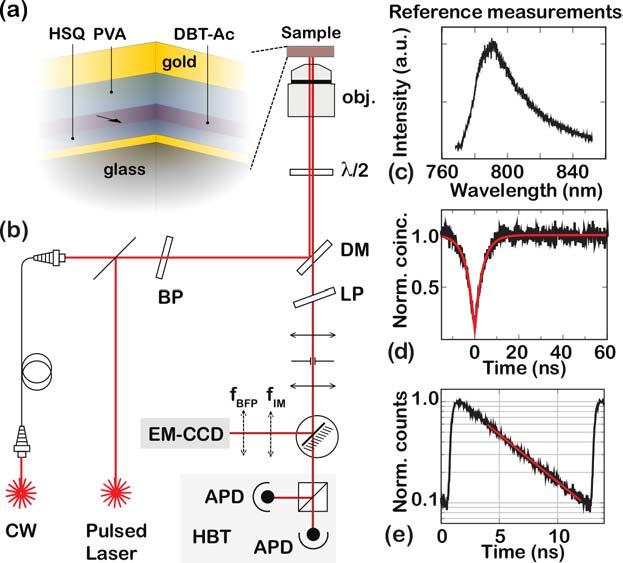
7 Our samples were obtained by embedding a 50-nm-thick anthracene (Ac) layer containing isolated dibenzoterrylene (DBT) molecules within dielectric spacers and metal layers, as exemplified in Figure 2a. This host-matrix combination (DBT-Ac) has been extensively studied, and it exhibits long photostability at room temperature, emission in the near infrared (zero-phonon line at 785 nm), high brightness, and controlled dipole orientation and film thickness 28. All the samples were fabricated through the subsequent superposition of thin layers. The DBT-Ac layer and the spacer layers, namely, hydrogen silsesquioxane (HSQ) and polyvinyl alcohol (PVA) were deposited by spin-coating, while the gold layers were deposited by sputtering and physical vapor deposition. The thickness of each layer was investigated by interferometric microscopy (PVA) or atomic force microscopy (HSQ, Ac, gold). The DBT-Ac layer was prepared using the same procedure described in Ref. 28. PVA layers were prepared starting with water solutions of various concentrations that were then spin-coated at different velocities in order to obtain the desired thicknesses. For instance, 3% PVA was spin-coated at 5000 rpm for 120 s, with a ramp of 5 s at 1500 rpm, to obtain a thickness of 70 ± 4 nm. The thin films deposited were dried at ambient conditions. A HSQ resist with 2% concentration was used and spin-coated at 1500 rpm for 60 s, and then a baking procedure with a hotplate (150 C for 2 min and then 200 C for 8 min) and oven (400 C for one hour) allows us to reach a thickness of approximately 60 nm. By dry etching in Ar/O2 plasma, the film was thinned to a thickness of 50 ± 3 nm, which was confirmed by optical reflectometry. The emission profile was investigated at room temperature with the setup illustrated in Figure 2b. A continuous wave (CW) diode laser at 767 nm and a pulsed Ti:sapphire laser (50 fs-long pulses) were used for the excitation of the DBT molecules. A dichroic mirror (DM) and a long-pass (LP) filter in the collection path allow for the detection of the weak red-shifted fluorescence signal. The wave-vector distribution of the emitted light has been studied via BFP imaging 29. In particular, the actual system parameters result in an angular resolution that is equal to 4 in the worst case, i.e., at the edge of the NA. A conversion from the electron-multiplier charge-coupled device (EM-CCD) pixels into degrees was performed in order to make a comparison between the theoretical analysis and the experimental results. In the latter, we took into account the response function of the optical system. The setup is also equipped with a spectrometer, a 7
8 Hanbury Brown-Twiss (HBT) module and fast avalanche photodiodes (APDs) for the measurement of the emission spectrum, the single-photon statistics, and the lifetime and saturation curves, respectively. Results and discussion The radiation pattern of a Hertzian dipole in a homogeneous infinite medium is illustrated in Figures 1c and 1d by the black dotted curves. The dipole orientation is parallel to the object plane of a microscope objective and the power has been integrated over the azimuthal angle. It is well known that 50% of the emission propagates in the opposite direction away from the observer and a significant amount of power is radiated below an angle of 90, which even lies outside the collection angle of a high-na objective. Therefore, the first step in our design has been to consider the modification of the radiation pattern when a metallic mirror, denoted as the reflector, is placed below the Hertzian dipole, which is represented by a black arrow in Figure 1a. We identify three possible configurations as a function of the distance d 1 between the emitter and reflector. For d 1 «λ/n, where λ is the emission wavelength and n the refractive index of the medium, the power is mostly transferred to the metal by absorption or excitation of surface plasmon polaritons, or the emission is suppressed by destructive interference with the image dipole, by assuming the metal is a perfect mirror 30. In both cases, quenching of the emission is observed. In the opposite extreme case, for d 1» λ/n, multiple interference, which occurs between the light directly emitted by the Hertzian dipole and the light reflected by the metal, gives rise to an emission pattern that may present various lobes and is hence unsuitable for efficient light collection. In our work, we focus on the intermediate values of d 1, for which we have calculated the radiation pattern and the total emitted power with a semi-analytical approach, as described in the Materials and Methods section. The introduction of a reflector element substantially directs the emission of a Hertzian dipole, as shown in Figure 1c for d 1 = 80 nm λ/(6n), λ = 785 nm and n = 1.5. Intuitively, these results can be explained in terms of the image dipole induced in the reflector by the source. When the two dipoles radiate with an appropriate 8
9 phase difference, which depends on λ/n, d 1 and the optical constants of the reflector, they constructively interfere in the forward direction, which results in a beaming effect 31. For a strongly reflective mirror, such as a 100 nm-thick gold film in the near infrared 32, we have found that beaming occurs in the range of λ/6n d 1 λ/4n. For λ = 785 nm and n = 1.5, this range spans approximately 50 nm, which can be easily controlled with state-of-the-art technology. The directionality can be improved by placing a second semi-reflective film at an appropriate distance d 2 from the Hertzian dipole (see Figure 1b and 1d), which functions as a passive antenna element. In practice, the field emitted by the dipole induced in such an element constructively interferes with that of the source in the forward direction and beams the radiation pattern in a similar manner as a director does in a Yagi-Uda configuration 31. We have found that with a 20-nm thick gold film, the emission is channeled into a single lobe, which has a width with a semi-angle of approximately 24, as shown in Figure 1d, when d 1 = 130 nm and d 2 = 70 nm. We remark that this occurs even for a randomly oriented dipole, mainly because the two dipole orientations in the plane are equivalent for a planar structure. Investigating the radiation pattern as a function of the thickness of the director, we find that for very thin films, i.e., for films thinner than approximately 5 nm, or for films thicker than 40 nm, the antenna performance worsens either because the beaming effect disappears or the transmission through the gold film becomes extremely small (see the Supplementary Information). To quantify the efficiency of our structures, in Figure 1e, we plot the collected power integrated over the azimuthal coordinate (P coll ) as a function of the collection angle. There is a substantial gain in P coll with respect to the homogeneous case (black dotted curve), especially for the configuration with the reflector and detector (blue solid curve) and for small angles. Moreover, this holds for a randomly oriented dipole (blue dashed curve). All curves in Figure 1 are normalized to the total radiated power in a homogeneous infinite medium with a refractive index of 1.5 (P hom ). When the collection angle is 90, P coll /P hom reaches a value of 0.6 for the case with only a reflector (see Figure 1a) and approximately 1.2 for the case with the reflector and director (see Figure 1b). Deviations of P coll /P hom at 90 from unity primarily occur because the 9
10 Hertzian dipole experiences a modification of the radiative rate, which will be analyzed. We remark that our designs represent an improvement in collection efficiency by more than one order of magnitude when considering the coupling to standard multimode fibers, for which NA = 0.4 is typical. Likewise, the excitation efficiency is improved and, by matching the spatial profile of the emitter with that of a focused laser beam, the antenna allows for lower pump powers, which in turn implies that a better signal to noise ratio is achieved. At microwave frequencies, a metallic grid placed near a ground plate turns a Fabry-Perot cavity into an antenna with high directionality 33. Scaling such structures to optical wavelengths would not be trivial due to the excitation of surface plasmon-polaritons in hole arrays, which affects the light emission and its spatial redistribution 34,35. On the contrary, the element director in our geometry is a homogeneous thin film, which makes the lateral position of the dipole irrelevant, prevents complex plasmonic effects and precludes the need for nanofabrication tools. This is also in contrast to the typical optical Yagi-Uda antenna, where the position of the quantum emitter must be controlled with nanometer accuracy with respect to the feeding element 18,36. Furthermore, we note that our antenna performance is only weakly dependent on the wavelength, and hence, it cannot correctly be described using a cavity effect 37. Finally, the constructive interference, which gives rise to the beaming effect, corresponds to a non-resonant condition for the equivalent cavity (we operate more than a FWHM away from resonance, which is calculated from the transmission of a plane wave under normal incidence). Conversely, no beaming of the emission pattern is predicted at resonance, as determined by numerical simulations reported in the Supplementary Information. The reference for our experiments is a 50-nm-thick DBT-Ac layer deposited on a glass cover slip. The emission spectrum, measured with a standard spectrometer, is shown in Figure 2c. The zero-phonon-line (ZPL) is found at λ = 785 nm and the spectrum exhibits a full-width at half-maximum (FWHM) of approximately 50 nm. The second-order intensity autocorrelation function, which is measured with a Hanbury Brown-Twiss setup, provides evidence of single-molecule emission, with a signal suppression of 98% at zero delay (as observed in Figure 2d, where no background subtraction has been applied). With a 10
11 standard time-correlated single photon counting scheme, time-resolved fluorescence decay curves are obtained, such as the curve plotted in Figure 2e, and hence, from a single exponential fit, the excited-state lifetime of the molecule is estimated. A statistical analysis of the lifetime distribution in the reference can be found in previous work 38, which yields an average value of 4.1 ± 0.4 ns for the excited-state lifetime. In the DBT-Ac system, the molecule is oriented parallel to the Ac film, which simplifies the comparison between the BFP measurements and the theoretical predictions. The main results are presented in Figure 3, where the upper panels correspond to experimental BFP images integrated over the emission spectrum and the bottom panels correspond to calculations obtained for λ = 785 nm. The corresponding structures, which are sketched in the top part of Figure 3, from left to right are as follows: (Reference) a 50 nm-thick DBT-Ac film deposited on top of a glass cover slip; (Single mirror) a 50 nm-thick DBT-Ac film separated from a 100 nm-thick gold film by a 70 nm-thick PVA layer; (Single mirror 2) the previous configuration with a 300 nm-thick PVA layer; (Double mirror) the antenna depicted in Figure 2b with a glass cover slip followed by a 20 nm-thick gold film, an annealed 50-nm-thick HSQ layer, a 50 nm-thick DBT-Ac layer, a 70 nm-thick PVA layer and 100 nm-thick gold film. Note that all layers between the reflector and director in this configuration have very similar refractive indices. All thicknesses refer to growth parameters that were verified using atomic force microscopy and interferometric techniques (see the Materials and Methods section for details). Fluctuations can occur, but they have not significantly influenced the emission, which proves the robustness of the beaming effect. Therefore, the parameters relevant to the double mirror configuration have been selected in such a way that beaming is observed for most of the investigated molecules, although it is dispersed at different positions inside the host matrix. However, this geometry does not maximize the total emitted power, which is discussed later with respect to Figure 4c. The experimental results are compared with our model along linear cuts taken in the direction perpendicular to the dipole orientation (see Figures 3e-h). The theoretical data are shown for two extreme cases with the DBT molecule lying 2 nm below the top or above the bottom surface of the Ac layer, which are represented by the green and blue curves, respectively. The double-lobe characteristic of a horizontally oriented dipole 11
12 placed in close proximity to a dielectric interface 39 is visible in Figures 3a, 3e and 3i. The addition of a reflector can create completely different radiation profiles. For a PVA thickness of 70 nm, Figures 3b, 3f and 3j show that the emission pattern is confined in one central lobe. However, Figures 3c, 3g and 3k show that for a PVA thickness of 300 nm, most of the emission falls outside the NA of the objective (1.4), which is represented by a white circle. Finally, the antenna with the reflector and director is presented in Figures 3d, 3h and 3l. In this case, the emission from a single DBT molecule in our planar optical antenna amounts to a semi-angle of only 20 at half maximum. This corresponds to a collection efficiency of 43% at 24 and 90% at 56. In all four cases, we observe good agreement between the experimental findings and the theoretical calculations, while assuming nominal parameters for the layer thicknesses and considering the uncertainty in the position of the DBT molecule within the Ac crystal, as well as the transfer function of the setup. In particular, a step truncation in any of the Fourier planes, which is given by the finite size of the objective, corresponds to smoothing and the occurrence of ripples at the edges of the NA. The anti-reflection coating of the objective exhibits strong wavelength dependence at large angles, as shown in the Supplementary Information. The reported curves are not corrected for the transfer function of the setup, and the invalid region is shaded in grey. Overall, we can reliably compare the theoretical and experimental results up to approximately 55, which is the angle at which the transmission reduces by a factor of two. Note that the apparent discrepancy between theory and experiment for the Single mirror 2 configuration is due to the normalization values, which differ because of the maximum measurable angle. All the experimental measurements fall within the theoretical curves that account for the possible positions of the DBT molecule in the Ac film. The robustness and versatility of the directive antenna analyzed in Figure 3d has been verified by performing additional theoretical and experimental analysis. First, we characterized the spontaneous emission rate of the DBT molecule to rule out coupling to cavity-like modes of the structure with the reflector and director, as well as to quantify enhancement or quenching of the fluorescence. Statistics of the lifetime measurements 12
13 have been collected and compared to an experimental reference sample 38. The average value and standard deviation from the data set reported in Figure 4a yield a lifetime of 3.8 ± 0.4 ns for DBT in the antenna configuration, and this value is perfectly comparable to that of the reference. From a theoretical point of view, this is consistent with the calculations of the total emitted power by a Hertzian dipole (P tot ), which is inversely proportional to the excited state lifetime and yields similar results in the two cases. In addition, this view is confirmed by the measurement of the saturation curve (Figure 4b), which exhibits comparable values for the maximum collected power. Specifically, the count rates at saturation are 3.1 ± 0.5 Mcps for the reference sample of Figure 3a and 2.8 ± 0.7 Mcps for the directional antenna of Figure 3d. This is consistent with comparable decay rates and similar losses in both cases. For the reference sample, the collection efficiency is limited by the objective NA; however, in the antenna structure, we have calculated an efficiency on the order of 55%, which varies as a function of the dipole position and multilayer geometrical parameters. The excitation efficiency is sensitive to the mode matching conditions. As a consequence of reciprocity, the radiation pattern of an antenna is equal to its receiving pattern. The relationship holds here because of the broadband performance of our design. Moreover, the blue-shifted excitation experiences a small field enhancement in the antenna. Hence, the interaction with the molecule has improved due to better mode matching and field concentration. In particular, we report a saturation power (P s ) that is a factor of 12 smaller for molecules within the antenna of Figure 3d compared to the reference sample of Figure 3a, i.e., P s decreases from 32 ± 8 µw to 2.6 ± 0.7 µw. Other emitter configurations would result in different combinations of beaming and excitation enhancement. A certain flexibility in finding an optimal trade-off stems from the fact that many configurations yield similar radiation patterns (see the Supplementary Information). All our data confirm the view that the modified emission profile yields an increased coupling efficiency, e.g., with a weakly focused laser beam or an optical fiber. In Figure 4c, we analyze the antenna efficiency (P rad /P tot ) by considering P tot and P rad as a function of the dipole distance to the reflector (blue and red solid curves, respectively). Here, the overall sample thickness is 13
14 kept constant (d 1 + d 2 = 200 nm), and the geometrical parameters are those of Figure 1b. In particular, the antenna working region is defined around d 1 = 130 nm, and it corresponds to an intensity that is approximately 70% higher than the intensity for a dipole in a homogeneous medium with the same refractive index n = 1.5. The antenna efficiency for this set of parameters is 65%. P rad / P tot reaches 70% at approximately d 1 = 80 nm and it remains above 50% for d 1 values between 30 nm and 160 nm, which largely shows that the efficiency of our antenna is large and weakly dependent on the dipole position. For applications where losses are critical, different materials and designs must be devised. In general, absorption losses, the presence of guided modes in dielectric layers or the excitation of surface plasmon polaritons reduce the antenna efficiency, as shown by the steep increase of P tot when the dipole approaches the metal layers. To stress this point, in the same figure, we plot the power absorbed by the reflector (P abs, blue dashed curve), computed in the quasi-static approximation, for the configuration of Figure 1a (Single mirror). These effects can also be observed in the power densities displayed in the Supplementary Information. Lastly, we notice that the power radiated by a Hertzian dipole near a perfect mirror (P rad, red dashed curve) is compatible with the calculations for P coll in Figure 1e, which results in approximately 60% of P hom for collection up to 90. This illustrates another mechanism for the reduction of P coll : when the source is near the reflector (or the director), the induced image dipole tends to decrease P tot, which is equal to P rad for an ideal metal. Therefore, we remark that reported single-molecule lifetime experiments near a silver mirror have been in excellent agreement with the classical theory 40. We deduce that the high intensity collected at small angles from our optical antenna stems from the directional emission rather than from an overall fluorescence enhancement. Finally, in order to stress the robustness of the proposed device, as a figure of merit, we considered P coll /P rad within an angle of 24, which corresponds to the NA of a standard multimode optical fiber. We found a wide range of dipole positions in which the efficiency is larger than 60%, even when P rad slightly decreases (e.g., as observed in Figure 4c for values of d 1 smaller than 100 nm). We also investigated P coll as a function of d 1 and d 2 for a 20 nm-thick gold director. We observe that more than one configuration leads to similar results, and in particular, whenever the total antenna length is increased by integer multiples of λ/2n. For example, for d 1 14
15 130 nm and d nm the directionality is even higher, and the radiation pattern has a semi-angle of 12 at half maximum. In contrast, P coll /P hom is only 0.5 in this case. Given n = 1.5 and collection in air, a total length larger than approximately 1.5 µm leads to a smearing out of the beaming effect because of the presence of lobes at higher angles (see the Supplementary Information). The large bandwidth of the directive antenna can be observed from Figure 4d, where P coll /P hom is reported as a function of the wavelength. The antenna bandwidth, which we define as the FWHM of P coll /P hom for θ = 24, can be estimated from the red curve in Figure 4d, and it is approximately 80 nm at approximately 785 nm. We remark that the beaming effect can be understood as a first approximation of the interference between the Hertzian dipole and its image charges, which are induced in the reflector and director elements. In particular, we have targeted the constructive interference under small angles in the outgoing direction from the director. This condition does not maximize the field between the two mirrors, as in the case of a resonant cavity. We first established a minimum distance between the dipole and the metal layers to exclude quenching effects and performed calculations starting with an educated guess of a distance of approximately λ/4n from the reflector, which maximizes forward scattering. This sets a range of values for the dipole position from the reflector. Then, we scanned the overall reflector-director distance and recorded both the emission pattern as well as the radiation efficiency to establish the optimal conditions. There is clearly a trade-off between a weak modulation of the density of states, which affects P tot, the efficiency (P rad /P tot ), as inferred from Figure 4c, and the modified radiation pattern, which determines the fraction of P rad collected within a given solid angle. Although our geometry is very similar to a Fabry-Pérot cavity, we would like to note the following observations. For the configuration in Figure 4d, we observed a threefold maximum enhancement of P tot with respect to an infinite medium and a broad resonance with a FWHM larger than 100 nm (blue dashed curve). Interestingly, by calculating the power density as a function of the wave vector (see Supplementary Information), one observes that it contains the contribution of surface plasmon polaritons, which corresponds to approximately half of P tot. However, the Purcell enhancement of the cavity would not correctly describe the operation, as we work more than a FWHM away from the resonant condition. Our design, which maximizes the constructive interference in the output direction 15
16 around small angles, is clearly distinct from the design of resonant antennas, which maximizes the field inside the structure or analogously P tot and P rad. Such a difference can be perceived, for instance, by comparing the spectral position of the maxima in Figure 4d for the total collected power (blue curve) and that collected within 24 o of the semi-angle θ (red curve). Further insight is provided in the Supplementary Information, where the near-field intensity is displayed for the structure that exhibits wave beaming effects and shown at the resonant wavelength of the equivalent cavity. Clearly, no beaming effect is observed for a resonant dipole. Finally, both theoretical and experimental investigations show neither appreciable enhancement nor reduction in the emission rate compared to that of the reference. We thus conclude that when beaming occurs, the density of states is only weakly altered by the presence of the mirror and director elements. Conclusions We have proposed a planar optical antenna design that strongly directs the radiation of quantum emitters. We have discussed the conditions that give rise to such an effect and provided experimental evidence of our theoretical findings, which shows that the beaming of light from a single molecule in a semi-cone is only 20 wide. The emission pattern resembles a weakly focused Gaussian laser beam or the radiation profile of a multimode fiber. This can significantly improve the collection and excitation of quantum emitters. The operating principle is similar to that of a Yagi-Uda antenna 31, where in place of resonant elements, such as nanoparticles 18,36, we make use of the dipoles induced in the reflector and director, which are made of thin metal films. This leads to a significant simplification of the structure and a much higher tolerance in selecting the geometrical parameters. In addition, the measured radiation patterns are narrower than in recent experimental demonstrations based on more sophisticated optical antennas 18,21,23,41. Furthermore, our device is compatible with collection in free space, and it can be easily applied to other quantum emitters, such as fluorescent dyes 42, quantum dots 43, and color centers 44, or scaled to other wavelengths. Because of 16
17 its performance and simplicity, it is likely that such a design will immediately find broad applications in spectroscopy, sensing and quantum optics. Acknowledgments The authors would like to thank V. Greco and A. Sordini for measuring the thickness of the thin films, B. Tiribilli, F. Dinelli and A. Flatae for inspection of the samples by atomic force microscopy, D.S. Wiersma for access to clean room facilities, M. Bellini and C. Corsi for Ti:sapphire operation, G. Mazzamuto for technical help and discussion and M. Gurioli for stimulating discussions. This work benefited from the COST Action MP1403 Nanoscale Quantum Optics, which is supported by COST (European Cooperation in Science and Technology). Competing Interests M.A., S.C., P.L., S.R., F.S. and C.T. have filed the patent application Device for the beaming of light emitted by light sources, in particular fluorescence of molecules, Patent pending PCT/EP2016/ filed on Author Contributions M.A. and C.T. conceived, planned and supervised the project. F.S. performed preliminary numerical simulations of the structure with the reflector. S.C. theoretically investigated and designed the structures with the semi-analytical approach described in the Methods section. S.C. and S.R. fabricated the samples. N.G. and W.P. provided glass cover slips with thin gold films and HSQ. S.C., P.L. and S.R. performed back focal plane, autocorrelation and saturation measurements, with the help of F.D. for the lifetime experiments. 17
18 M.A., S.C., P.L. and C.T. analyzed the data and discussed them with all authors. M.A., S.C. and C.T. wrote the manuscript with feedback from all authors. Supplementary Information accompanies the manuscript on the Light: Science & Applications website ( 18
19 References 1 Vahala KJ. Optical microcavities. Nature 2003; 424: Lecamp G, Lalanne P, Hugonin JP. Very large spontaneous-emission β factors in photonic-crystal waveguides. Phys Rev Lett 2007; 99: Quan QM, Bulu I, Lončar M. Broadband waveguide QED system on a chip. Phys Rev A 2009; 80: Lee KG, Chen XW, Eghlidi H, Kukura P, Lettow R et al. A planar dielectric antenna for directional single-photon emission and near-unity collection efficiency. Nat Photon 2011; 5: Chu XL, Brenner TJK, Chen XW, Ghosh Y, Hollingsworth JA et al. Experimental realization of an optical antenna designed for collecting 99% of photons from a quantum emitter. Optica 2014; 1: Ma Y, Kremer PE, Gerardot BD. Efficient photon extraction from a quantum dot in a broad-band planar cavity antenna. J Appl Phys 2014; 115: Barnes WL, Björk G, Gérard JM, Jonsson P, Wasey JAE et al. Solid-state single photon sources: light collection strategies. Eur Phys J D 2002; 18: Chunnilall CJ, Degiovanni IP, Kück S, Müller I, Sinclair AG. Metrology of single-photon sources and detectors: a review. Opt Eng 2014; 53: Lichtman WJ, Conchello JA. Fluorescence microscopy. Nat Methods 2005; 2: Lakowicz RJ. Principles of Fluorescence Spectroscopy. Berlin, Heidelberg: Springer; Holmes-Smith AS. Introduction to special issue on fluorescence-based sensing technologies. Biosensors 19
20 2015; 5: Steinmetz T, Colombe Y, Hunger D, Häns TW, Balocchi A et al. Stable fiber-based Fabry-Pérot cavity. Appl Phys Lett 2006; 89: Toninelli C, Delley Y, Stöferle T, Renn A, Götzinger S et al. A scanning microcavity for in situ control of single-molecule emission. Appl Phys Lett 2010; 97: Kelkar H, Wang D, Martín-Cano D, Hoffmann B, Christiansen S et al. Sensing nanoparticles with a cantilever-based scannable optical cavity of low finesse and sub-λ 3 volume. Phys Rev Appl 2015; 4: Zumofen G, Mojarad NM, Sandoghdar V, Agio M. Perfect reflection of light by an oscillating dipole. Phys Rev Lett 2008; 101: Wrigge G, Gerhardt I, Hwang J, Zumofen G, Sandoghdar V. Efficient coupling of photons to a single molecule and the observation of its resonance fluorescence. Nat Phys 2008; 4: Kühn S, Mori G, Agio M, Sandoghdar V. Modification of single molecule fluorescence close to a nanostructure: radiation pattern, spontaneous emission and quenching. Mol Phys 2008; 106: Curto AG, Volpe G, Taminiau TH, Kreuzer MP, Quidant R et al. Unidirectional emission of a quantum dot coupled to a nanoantenna. Science 2010; 329: Kosako T, Kadoya Y, Hofmann HF. Directional control of light by a nano-optical Yagi-Uda antenna. Nat Photon 2010; 4: Dregely D, Taubert R, Dorfmüller J, Vogelgesang R, Kern K et al. 3D optical Yagi Uda nanoantenna array. Nat Commun 2011; 2:
21 21 Claudon J, Bleuse J, Malik NS, Bazin M, Jaffrennou P et al. A highly efficient single-photon source based on a quantum dot in a photonic nanowire. Nat Photon 2010; 4: Shegai T, Miljković VD, Bao K, Xu HX, Nordlander P et al. Unidirectional broadband light emission from supported plasmonic nanowires. Nano Lett 2011; 11: Akselrod GM, Argyropoulos C, Hoang TB, Ciracì C, Fang C et al. Probing the mechanisms of large Purcell enhancement in plasmonic nanoantennas. Nat Photon 2014; 8: Esteban R, Teperik TV, Greffet JJ. Optical patch antennas for single photon emission using surface plasmon resonances. Phys Rev Lett 2010; 104: Tong L, Pakizeh L, Feuz L, Dmitriev A. Highly directional bottom-up 3D nanoantenna for visible light. Sci Rep 2013; 3: Neyts KA. Simulation of light emission from thin-film microcavities. J Opt Soc Am A 1998; 15: Chen XW, Choy WC, He SL. Efficient and rigorous modeling of light emission in planar multilayer organic light-emitting diodes. J Display Technol 2007; 3: Toninelli C, Early K, Bremi J, Renn A, Götzinger S et al. Near-infrared single-photons from aligned molecules in ultrathin crystalline films at room temperature. Opt Express 2010; 18: Lieb MA, Zavislan JM, Novotny L. Single-molecule orientations determined by direct emission pattern imaging. J Opt Soc Am B 2004; 21: Chance RR, Prock A, Silbey R. Molecular fluorescence and energy transfer near interfaces. In: Prigogine I, Rice SA (eds). Advances in Chemical Physics, Volume 37. New York: John Wiley & Sons; 1978: Balanis CA. Antenna Theory: Analysis and Design. 3rd edn. Hoboken, NJ: John Wiley & Sons;
22 32 Johnson PB, Christy RW. Optical constants of the noble metals. Phys Rev B 1972; 6: Guerin N, Enoch S, Tayeb G, Sabouroux P, Vincent P et al. A metallic Fabry-Perot directive antenna. IEEE Trans Antennas Propag 2006; 54: Garcìa-Vidal FJ, Martìn-Moreno L, Ebbesen TW, Kuipers L. Light passing through subwavelength apertures. Rev Mod Phys 2010; 82: McDaniel S, Blair S. Increased OLED radiative efficiency using a directive optical antenna. Opt Express 2010; 18: Li JJ, Salandrino A, Engheta N. Shaping light beams in the nanometer scale: A Yagi-Uda nanoantenna in the optical domain. Phys Rev B 2007; 76: Chizhik A, Schleifenbaum F, Gutbro R, Chizhik A, Khoptyar D et al. Tuning the fluorescence emission spectra of a single molecule with a variable optical subwavelength metal microcavity. Phys Rev Lett 2009; 102: Mazzamuto G, Tabani A, Pazzagli S, Rizvi S, Reserbat-Plantey A et al. Single-molecule study for a graphene-based nano-position sensor. New J Phys 2014; 16: Arnoldus HF, Foley JT. Transmission of dipole radiation through interfaces and the phenomenon of anticritical angles. J Opt Soc Am A 2004; 21: Buchler BC, Kalkbrenner T, Hettich C, Sandoghdar V. Measuring the quantum efficiency of the optical emission of single radiating dipoles using a scanning mirror. Phys Rev Lett 2005; 95: Pakizeh T, Käll M. Unidirectional ultracompact optical nanoantennas. Nano Lett 2009; 9: Zheng QS, Juette MF, Jockusch S, Wasserman MR, Zhou Z et al. Ultra-stable organic fluorophores for 22
23 single-molecule research. Chem Soc Rev 2014; 43: Alivisatos P. The use of nanocrystals in biological detection. Nat Biotechnol 2004; 22: Pezzagna S, Rogalla D, Wildanger D, Meijer J, Zaitsev A. Creation and nature of optical centres in diamond for single-photon emission overview and critical remarks. New J Phys 2011; 13:
24 List of Figures: Figure 1. Concept of a planar directional antenna and theoretical analysis. (a-b) Sketch of a planar directional antenna: the induced image-dipoles are identified by the red and the blue arrows in the reflector and in the director, respectively, while the source dipole is represented by a black arrow. The emitter is placed at distances d 1 and d 2 from the reflector and the director, respectively. In our study, the reflector and the director are 100-nm-thick and 20-nm-thick gold films, respectively. The medium above the reflector has a refractive index n = 1.5, while a semi-infinite top layer of air is considered (n = 1). (c-d) Radiation pattern integrated over the azimuthal coordinate as a function of the polar angle θ of a horizontal Hertzian dipole (HD), emitting at λ = 785 nm, coupled to the planar directional antenna of Figure 1a (d 1 = 80 nm) and b (d 1 = 130 nm and d 2 = 70 nm), respectively. The two curves are normalized by the maximum value of the same quantity for a dipole in a homogeneous medium with refractive index n = 1.5, which is also shown by the black dotted curves. (e) Normalized power (P coll /P hom ) as a function of the collection angle for the configurations of Figures 1a-d. The normalized power for a Hertzian dipole with random orientation (RD) is shown by the blue dashed curve. P hom is the total power emitted by a Hertzian dipole in a homogeneous medium of refractive index n =
25 Figure 2. Experimental setup and sample characterization. (a) Sketch of the experimental setup for single-molecule spectroscopy, and BFP imaging. (b) Layout of the sample containing a DBT-Ac film inside the planar optical antenna. (c) Fluorescence spectrum of a single DBT molecule in an Ac crystalline film deposited on a glass cover slip. (d) For the same configuration, secondorder intensity autocorrelation function measured with a Hanbury Brown-Twiss setup and (e) time-resolved fluorescence decay curve. From the single exponential fit (red line), one obtains the excited-state lifetime for the molecule. 25
26 Figure 3. Experimental results and comparison with theory. (a)-(d) Sketches of the samples and corresponding normalized BFP images of a single DBT molecule acquired with an EM-CCD camera. (e)-(h) Comparison between calculated emission patterns for λ = 785 nm and crosssections of the experimental BFP images. The shaded areas represent the objective transfer function, from a transmission of 0 (gray) to 1 (white). The two theoretical curves for each case correspond to different positions of the DBT molecule in a 50 nm-thick Ac film: 2 nm from the top interface (blue curve) and 2 nm from the bottom interface (green curve). Both the theoretical and experimental curves have been normalized to 1, except for the experimental curve of (g), which is normalized in order to match the theoretical value at 0 (the dipole position at 2 nm). (i)-(l) Theoretical BFP images that reproduce the experimental results. The plots are normalized with respect to the maximum value of the radiation pattern of a Hertzian dipole in a homogeneous medium with n = 1.5. The white circles show the nominal NA of the collection optics (θ = 67 ). (a), (e), (i) Experimental reference case with glass cover slip (n glass = 1.52), 50 nm DBT-Ac (n Ac = 1.6) and air (n air = 1); (b), (f), (j) System with reflector, composed of a semi-infinite glass cover slip, 50 nm DBT-Ac, 70 nm PVA (n PVA = 1.49), 100 nm gold and air; (c), (g), (k) Same configuration as before, but with 300 nm-thick PVA layer; (d), (h), (l) System with director and reflector, composed of a semi-infinite glass cover slip, 20 nm gold, 50 nm HSQ (n HSQ = 1.4), 50 nm DBT-Ac, 70 nm PVA, 100 nm gold and air. 26
27 Figure 4. Further analyses of antenna robustness (a) Statistical distribution of the excited-state lifetime of a DBT molecule in an Ac crystalline film, which is coupled to our planar optical antenna with the director and reflector, as shown in Figure 2b. (b) Typical saturation curves obtained for dipoles in the reference sample and saturation curves obtained for the dipoles, which are coupled to the double mirror antenna. For the sake of clarity, the offset and linear dependence of leakage of the pump light are subtracted. The solid lines are fits for the data, which give maximal counts for R inf = (2.97 ± 0.08) x 10 6 and (2.89 ± 0.02) x 10 6, and the saturation power P s = (49 ± 4) x 10 µw and 47.0 ± 1.4 µw, for the reference and antenna configurations, respectively. (c) Normalized powers associated with a Hertzian dipole at λ = 785 nm in a medium with refractive index n = 1.5 at a distance d 1 from a reflector. The distance between the 100 nm-thick gold reflector and a 20 nm-thick gold director is kept constant at 200 nm. The blue solid curve refers to the total power emitted by the dipole in the antenna (P tot /P hom ), whereas the red solid curve represents the power transmitted (radiated) in the upper medium above the director (P rad /P hom ). The blue dashed curve represents power absorption (P abs /P hom ) by energy transfer to the reflector, while the red dashed curve represents P tot /P hom for the case where the Hertzian dipole is in front of a perfect mirror. The media below the reflector and above the director are air and glass, respectively. (d) Normalized collected power P coll /P hom up to θ = 24 (red solid curve) and θ = 90 (blue solid curve) as a function of wavelength for d 1 = 130 nm and the antenna parameters of Figure 4c, except that the external media are interchanged. P coll /P hom up to θ = 90 is also shown for a Hertzian dipole in glass (black dotted curve) or 130 nm from a gold reflector (red dashed curve). 27
 Reflector(HD) Reflector+Director(HD) Reflector+Director(RD) 0.")
28 (a) (c) x (b) (d) x (e) P coll /P hom Homogeneous(HD) Reflector(HD) Reflector+Director(HD) Reflector+Director(RD) Collection angle(deg)
29
 1 1 (b) 1")
 10 30 50 70 90 10 30 50 70 90 10 30 50 70 90 Polar angle (deg) Polar")
 Intensity (P/P hom ) Single mirror Single mirror 2 Double mirror 1 0 Intensity (a.")
 Intensity (P/P hom ) 0.9 theo 2 nm 0.7 theo 48 nm exp 0.5 0.")
30 Intensity (a.u.) Reference DBT-Ac DBT-Ac glass glass DBT-Ac glass PVA PVA gold gold (a) 1 1 (b) 1 (c) (d) (e) (f) (g) (h) (i) Polar angle (deg) Polar angle (deg) Polar angle (deg) (j) (k) 3 9 (l) Intensity (a.u.) Intensity (a.u.) Intensity (P/P hom ) Single mirror Single mirror 2 Double mirror 1 0 Intensity (a.u.) Intensity (a.u.) Intensity (P/P hom ) Intensity (a.u.) 3 0 Intensity (a.u.) Intensity (P/P hom ) 0.9 theo 2 nm 0.7 theo 48 nm exp HSQ DBT-Ac glass gold PVA Polar angle (deg) 1 Intensity (a.u.) Intensity (P/P hom )
31 (a) (c) Occurrence P/P hom Lifetime (ns) P abs (refl. + dir.) P tot Distance d 1 (nm) (b) (d) (mirror) P tot (refl. + dir.) P rad Counts/s (10 6 ) P coll /P hom (refl. + dir.) P θ=90 (refl. + dir.) P θ=24 reference refl. + dir Power (mw) (refl. + dir.) P tot Wavelength (nm) (refl.) P θ=90 (glass) P θ=90
Supplementary Information
 Supplementary Information Beaming light from a quantum emitter with a planar optical antenna Simona Checcucci, 1,2,3,4 Pietro Lombardi, 1,2,3 Sahrish Rizvi, 1 Fabrizio Sgrignuoli, 1,3 Nico Gruhler, 5,6
Cavity QED with quantum dots in semiconductor microcavities
 Cavity QED with quantum dots in semiconductor microcavities M. T. Rakher*, S. Strauf, Y. Choi, N.G. Stolz, K.J. Hennessey, H. Kim, A. Badolato, L.A. Coldren, E.L. Hu, P.M. Petroff, D. Bouwmeester University
Single-photon excitation of morphology dependent resonance
 Single-photon excitation of morphology dependent resonance 3.1 Introduction The examination of morphology dependent resonance (MDR) has been of considerable importance to many fields in optical science.
Nd:YSO resonator array Transmission spectrum (a. u.) Supplementary Figure 1. An array of nano-beam resonators fabricated in Nd:YSO.
 Supplementary Figure 1. An array of nano-beam resonators fabricated in Nd:YSO.") a Nd:YSO resonator array µm Transmission spectrum (a. u.) b 4 F3/2-4I9/2 25 2 5 5 875 88 λ(nm) 885 Supplementary Figure. An array of nano-beam resonators fabricated in Nd:YSO. (a) Scanning electron microscope
a Nd:YSO resonator array µm Transmission spectrum (a. u.) b 4 F3/2-4I9/2 25 2 5 5 875 88 λ(nm) 885 Supplementary Figure. An array of nano-beam resonators fabricated in Nd:YSO. (a) Scanning electron microscope
Direct observation of beamed Raman scattering
 Supporting Information Direct observation of beamed Raman scattering Wenqi Zhu, Dongxing Wang, and Kenneth B. Crozier* School of Engineering and Applied Sciences, Harvard University, Cambridge, Massachusetts
SUPPLEMENTARY INFORMATION
 SUPPLEMENTARY INFORMATION DOI: 10.1038/NNANO.2015.137 Controlled steering of Cherenkov surface plasmon wakes with a one-dimensional metamaterial Patrice Genevet *, Daniel Wintz *, Antonio Ambrosio *, Alan
attosnom I: Topography and Force Images NANOSCOPY APPLICATION NOTE M06 RELATED PRODUCTS G
 APPLICATION NOTE M06 attosnom I: Topography and Force Images Scanning near-field optical microscopy is the outstanding technique to simultaneously measure the topography and the optical contrast of a sample.
Session 2: Silicon and Carbon Photonics (11:00 11:30, Huxley LT311)
") Session 2: Silicon and Carbon Photonics (11:00 11:30, Huxley LT311) (invited) Formation and control of silicon nanocrystals by ion-beams for photonic applications M Halsall The University of Manchester,
Session 2: Silicon and Carbon Photonics (11:00 11:30, Huxley LT311) (invited) Formation and control of silicon nanocrystals by ion-beams for photonic applications M Halsall The University of Manchester,
Measuring chromatic aberrations in imaging systems using plasmonic nano particles
 Measuring chromatic aberrations in imaging systems using plasmonic nano particles Sylvain D. Gennaro, Tyler R. Roschuk, Stefan A. Maier, and Rupert F. Oulton* Department of Physics, The Blackett Laboratory,
Supplementary Information for. Surface Waves. Angelo Angelini, Elsie Barakat, Peter Munzert, Luca Boarino, Natascia De Leo,
 Supplementary Information for Focusing and Extraction of Light mediated by Bloch Surface Waves Angelo Angelini, Elsie Barakat, Peter Munzert, Luca Boarino, Natascia De Leo, Emanuele Enrico, Fabrizio Giorgis,
Supplementary Figure 1. Effect of the spacer thickness on the resonance properties of the gold and silver metasurface layers.
 Supplementary Figure 1. Effect of the spacer thickness on the resonance properties of the gold and silver metasurface layers. Finite-difference time-domain calculations of the optical transmittance through
Supplementary Figure 1 Reflective and refractive behaviors of light with normal
 Supplementary Figures Supplementary Figure 1 Reflective and refractive behaviors of light with normal incidence in a three layer system. E 1 and E r are the complex amplitudes of the incident wave and
A novel tunable diode laser using volume holographic gratings
 A novel tunable diode laser using volume holographic gratings Christophe Moser *, Lawrence Ho and Frank Havermeyer Ondax, Inc. 85 E. Duarte Road, Monrovia, CA 9116, USA ABSTRACT We have developed a self-aligned
Single Photon Transistor. Brad Martin PH 464
 Single Photon Transistor Brad Martin PH 464 Brad Martin Single Photon Transistor 1 Abstract The concept of an optical transistor is not a new one. The difficulty with building optical devices that use
High-Resolution Bubble Printing of Quantum Dots
 SUPPORTING INFORMATION High-Resolution Bubble Printing of Quantum Dots Bharath Bangalore Rajeeva 1, Linhan Lin 1, Evan P. Perillo 2, Xiaolei Peng 1, William W. Yu 3, Andrew K. Dunn 2, Yuebing Zheng 1,*
Administrative details:
 Administrative details: Anything from your side? www.photonics.ethz.ch 1 What are we actually doing here? Optical imaging: Focusing by a lens Angular spectrum Paraxial approximation Gaussian beams Method
Supplementary Figure 1. GO thin film thickness characterization. The thickness of the prepared GO thin
 Supplementary Figure 1. GO thin film thickness characterization. The thickness of the prepared GO thin film is characterized by using an optical profiler (Bruker ContourGT InMotion). Inset: 3D optical
Supporting Information
 Supporting Information Mode imaging and selection in strongly coupled nanoantennas Jer-Shing Huang 1,*, Johannes Kern 1, Peter Geisler 1, Pia Weimann 2, Martin Kamp 2, Alfred Forchel 2, Paolo Biagioni
SUPPORTING INFORMATION
 SUPPORTING INFORMATION Plasmonic Nanopatch Array for Optical Integrated Circuit Applications Shi-Wei Qu & Zai-Ping Nie Table of Contents S.1 PMMA Loaded Coupled Wedge Plasmonic Waveguide (CWPWG) 2 S.2
Nanoscale Systems for Opto-Electronics
 Nanoscale Systems for Opto-Electronics 675 PL intensity [arb. units] 700 Wavelength [nm] 650 625 600 5µm 1.80 1.85 1.90 1.95 Energy [ev] 2.00 2.05 1 Nanoscale Systems for Opto-Electronics Lecture 5 Interaction
Impact of the light coupling on the sensing properties of photonic crystal cavity modes Kumar Saurav* a,b, Nicolas Le Thomas a,b,
 Impact of the light coupling on the sensing properties of photonic crystal cavity modes Kumar Saurav* a,b, Nicolas Le Thomas a,b, a Photonics Research Group, Ghent University-imec, Technologiepark-Zwijnaarde
SUPPLEMENTARY INFORMATION
 Supplementary Information S1. Theory of TPQI in a lossy directional coupler Following Barnett, et al. [24], we start with the probability of detecting one photon in each output of a lossy, symmetric beam
Lab4 Hanbury Brown and Twiss Setup. Photon Antibunching
 Lab4 Hanbury Brown and Twiss Setup. Photon Antibunching Shule Li Abstract Antibunching is a purely quantum effect and cannot be realized from the classical theory of light. By observing the antibunching
Multiple wavelength resonant grating filters at oblique incidence with broad angular acceptance
 Multiple wavelength resonant grating filters at oblique incidence with broad angular acceptance Andrew B. Greenwell, Sakoolkan Boonruang, M.G. Moharam College of Optics and Photonics - CREOL, University
Bias errors in PIV: the pixel locking effect revisited.
 Bias errors in PIV: the pixel locking effect revisited. E.F.J. Overmars 1, N.G.W. Warncke, C. Poelma and J. Westerweel 1: Laboratory for Aero & Hydrodynamics, University of Technology, Delft, The Netherlands,
TAPERED MEANDER SLOT ANTENNA FOR DUAL BAND PERSONAL WIRELESS COMMUNICATION SYSTEMS
 are closer to grazing, where 50. However, once the spectral current distribution is windowed, and the level of the edge singularity is reduced by this process, the computed RCS shows a much better agreement
Silicon-based photonic crystal nanocavity light emitters
 Silicon-based photonic crystal nanocavity light emitters Maria Makarova, Jelena Vuckovic, Hiroyuki Sanda, Yoshio Nishi Department of Electrical Engineering, Stanford University, Stanford, CA 94305-4088
Wavelength-independent coupler from fiber to an on-chip cavity, demonstrated over an 850nm span
 Wavelength-independent coupler from fiber to an on-chip, demonstrated over an 85nm span Tal Carmon, Steven Y. T. Wang, Eric P. Ostby and Kerry J. Vahala. Thomas J. Watson Laboratory of Applied Physics,
Compact hybrid TM-pass polarizer for silicon-on-insulator platform
 Compact hybrid TM-pass polarizer for silicon-on-insulator platform Muhammad Alam,* J. Stewart Aitchsion, and Mohammad Mojahedi Department of Electrical and Computer Engineering, University of Toronto,
Laser Beam Analysis Using Image Processing
 Journal of Computer Science 2 (): 09-3, 2006 ISSN 549-3636 Science Publications, 2006 Laser Beam Analysis Using Image Processing Yas A. Alsultanny Computer Science Department, Amman Arab University for
CHAPTER 5 FINE-TUNING OF AN ECDL WITH AN INTRACAVITY LIQUID CRYSTAL ELEMENT
 CHAPTER 5 FINE-TUNING OF AN ECDL WITH AN INTRACAVITY LIQUID CRYSTAL ELEMENT In this chapter, the experimental results for fine-tuning of the laser wavelength with an intracavity liquid crystal element
Single Photon Transistor. PH464 Spring 2009 Brad Martin
 Single Photon Transistor PH464 Spring 2009 Brad Martin Transistors A transistor in general is a 3 port device in which a control at one of those ports can manage the flow between the other 2 points. The
SUPPLEMENTARY INFORMATION
 SUPPLEMENTARY INFORMATION Supplementary Information Real-space imaging of transient carrier dynamics by nanoscale pump-probe microscopy Yasuhiko Terada, Shoji Yoshida, Osamu Takeuchi, and Hidemi Shigekawa*
Angle-resolved cathodoluminescence spectroscopy
 Angle-resolved cathodoluminescence spectroscopy Toon Coenen, Ernst Jan R. Vesseur, and Albert Polman Center for Nanophotonics, FOM Institute AMOLF Science Park 104, 1098 XG Amsterdam, The Netherlands Abstract
Basic concepts. Optical Sources (b) Optical Sources (a) Requirements for light sources (b) Requirements for light sources (a)
 Optical Sources (a) Requirements for light sources (b) Requirements for light sources (a)") Optical Sources (a) Optical Sources (b) The main light sources used with fibre optic systems are: Light-emitting diodes (LEDs) Semiconductor lasers (diode lasers) Fibre laser and other compact solid-state
Optical Sources (a) Optical Sources (b) The main light sources used with fibre optic systems are: Light-emitting diodes (LEDs) Semiconductor lasers (diode lasers) Fibre laser and other compact solid-state
Integrated into Nanowire Waveguides
 Supporting Information Widely Tunable Distributed Bragg Reflectors Integrated into Nanowire Waveguides Anthony Fu, 1,3 Hanwei Gao, 1,3,4 Petar Petrov, 1, Peidong Yang 1,2,3* 1 Department of Chemistry,
Spectral Analysis of the LUND/DMI Earthshine Telescope and Filters
 Spectral Analysis of the LUND/DMI Earthshine Telescope and Filters 12 August 2011-08-12 Ahmad Darudi & Rodrigo Badínez A1 1. Spectral Analysis of the telescope and Filters This section reports the characterization
arxiv:physics/ v1 [physics.optics] 28 Sep 2005
![arxiv:physics/ v1 [physics.optics] 28 Sep 2005](/thumbs/91/105523130.jpg "arxiv:physics/ v1 [physics.optics] 28 Sep 2005") Near-field enhancement and imaging in double cylindrical polariton-resonant structures: Enlarging perfect lens Pekka Alitalo, Stanislav Maslovski, and Sergei Tretyakov arxiv:physics/0509232v1 [physics.optics]
Near-field enhancement and imaging in double cylindrical polariton-resonant structures: Enlarging perfect lens Pekka Alitalo, Stanislav Maslovski, and Sergei Tretyakov arxiv:physics/0509232v1 [physics.optics]
Influence of dielectric substrate on the responsivity of microstrip dipole-antenna-coupled infrared microbolometers
 Influence of dielectric substrate on the responsivity of microstrip dipole-antenna-coupled infrared microbolometers Iulian Codreanu and Glenn D. Boreman We report on the influence of the dielectric substrate
Narrowing spectral width of green LED by GMR structure to expand color mixing field
 Narrowing spectral width of green LED by GMR structure to expand color mixing field S. H. Tu 1, Y. C. Lee 2, C. L. Hsu 1, W. P. Lin 1, M. L. Wu 1, T. S. Yang 1, J. Y. Chang 1 1. Department of Optical and
z t h l g 2009 John Wiley & Sons, Inc. Published 2009 by John Wiley & Sons, Inc.
 x w z t h l g Figure 10.1 Photoconductive switch in microstrip transmission-line geometry: (a) top view; (b) side view. Adapted from [579]. Copyright 1983, IEEE. I g G t C g V g V i V r t x u V t Z 0 Z
SUPPLEMENTARY INFORMATION
 Silver permittivity used in the simulations Silver permittivity values are obtained from Johnson & Christy s experimental data 31 and are fitted with a spline interpolation in order to estimate the permittivity
The electric field for the wave sketched in Fig. 3-1 can be written as
 ELECTROMAGNETIC WAVES Light consists of an electric field and a magnetic field that oscillate at very high rates, of the order of 10 14 Hz. These fields travel in wavelike fashion at very high speeds.
Frequency Tunable Low-Cost Microwave Absorber for EMI/EMC Application
 Progress In Electromagnetics Research Letters, Vol. 74, 47 52, 2018 Frequency Tunable Low-Cost Microwave Absorber for EMI/EMC Application Gobinda Sen * and Santanu Das Abstract A frequency tunable multi-layer
In their earliest form, bandpass filters
 Bandpass Filters Past and Present Bandpass filters are passive optical devices that control the flow of light. They can be used either to isolate certain wavelengths or colors, or to control the wavelengths
Printing Beyond srgb Color Gamut by. Mimicking Silicon Nanostructures in Free-Space
 Supporting Information for: Printing Beyond srgb Color Gamut by Mimicking Silicon Nanostructures in Free-Space Zhaogang Dong 1, Jinfa Ho 1, Ye Feng Yu 2, Yuan Hsing Fu 2, Ramón Paniagua-Dominguez 2, Sihao
ANALYSIS OF EPSILON-NEAR-ZERO METAMATE- RIAL SUPER-TUNNELING USING CASCADED ULTRA- NARROW WAVEGUIDE CHANNELS
 Progress In Electromagnetics Research M, Vol. 14, 113 121, 21 ANALYSIS OF EPSILON-NEAR-ZERO METAMATE- RIAL SUPER-TUNNELING USING CASCADED ULTRA- NARROW WAVEGUIDE CHANNELS J. Bai, S. Shi, and D. W. Prather
2. Pulsed Acoustic Microscopy and Picosecond Ultrasonics
 1st International Symposium on Laser Ultrasonics: Science, Technology and Applications July 16-18 2008, Montreal, Canada Picosecond Ultrasonic Microscopy of Semiconductor Nanostructures Thomas J GRIMSLEY
Acoustic resolution. photoacoustic Doppler velocimetry. in blood-mimicking fluids. Supplementary Information
 Acoustic resolution photoacoustic Doppler velocimetry in blood-mimicking fluids Joanna Brunker 1, *, Paul Beard 1 Supplementary Information 1 Department of Medical Physics and Biomedical Engineering, University
Plane wave excitation by taper array for optical leaky waveguide antenna
 LETTER IEICE Electronics Express, Vol.15, No.2, 1 6 Plane wave excitation by taper array for optical leaky waveguide antenna Hiroshi Hashiguchi a), Toshihiko Baba, and Hiroyuki Arai Graduate School of
Enhanced directional excitation and emission of single emitters by a nano-optical Yagi-Uda antenna.
 Enhanced directional excitation and emission of single emitters by a nano-optical Yagi-Uda antenna. Tim H. Taminiau*, Fernando D. Stefani, and Niek F. van Hulst # ICFO Institut de Ciences Fotoniques, Mediterranean
Spatial Investigation of Transverse Mode Turn-On Dynamics in VCSELs
 Spatial Investigation of Transverse Mode Turn-On Dynamics in VCSELs Safwat W.Z. Mahmoud Data transmission experiments with single-mode as well as multimode 85 nm VCSELs are carried out from a near-field
Waveguiding in PMMA photonic crystals
 ROMANIAN JOURNAL OF INFORMATION SCIENCE AND TECHNOLOGY Volume 12, Number 3, 2009, 308 316 Waveguiding in PMMA photonic crystals Daniela DRAGOMAN 1, Adrian DINESCU 2, Raluca MÜLLER2, Cristian KUSKO 2, Alex.
RECENTLY, using near-field scanning optical
 1 2 1 2 Theoretical and Experimental Study of Near-Field Beam Properties of High Power Laser Diodes W. D. Herzog, G. Ulu, B. B. Goldberg, and G. H. Vander Rhodes, M. S. Ünlü L. Brovelli, C. Harder Abstract
Long-distance propagation of short-wavelength spin waves. Liu et al.
 Long-distance propagation of short-wavelength spin waves Liu et al. Supplementary Note 1. Characterization of the YIG thin film Supplementary fig. 1 shows the characterization of the 20-nm-thick YIG film
Supporting Information
 Electronic Supplementary Material (ESI) for Materials Horizons. This journal is The Royal Society of Chemistry 2017 Supporting Information Nanofocusing of circularly polarized Bessel-type plasmon polaritons
SUPPLEMENTARY INFORMATION
 Transfer printing stacked nanomembrane lasers on silicon Hongjun Yang 1,3, Deyin Zhao 1, Santhad Chuwongin 1, Jung-Hun Seo 2, Weiquan Yang 1, Yichen Shuai 1, Jesper Berggren 4, Mattias Hammar 4, Zhenqiang
Investigation of the Near-field Distribution at Novel Nanometric Aperture Laser
 Investigation of the Near-field Distribution at Novel Nanometric Aperture Laser Tiejun Xu, Jia Wang, Liqun Sun, Jiying Xu, Qian Tian Presented at the th International Conference on Electronic Materials
Nanofluidic Refractive-Index Sensors Formed by Nanocavity Resonators in Metals without Plasmons
 Sensors 2011, 11, 2939-2945; doi:10.3390/s110302939 OPEN ACCESS sensors ISSN 1424-8220 www.mdpi.com/journal/sensors Article Nanofluidic Refractive-Index Sensors Formed by Nanocavity Resonators in Metals
NEW LASER ULTRASONIC INTERFEROMETER FOR INDUSTRIAL APPLICATIONS B.Pouet and S.Breugnot Bossa Nova Technologies; Venice, CA, USA
 NEW LASER ULTRASONIC INTERFEROMETER FOR INDUSTRIAL APPLICATIONS B.Pouet and S.Breugnot Bossa Nova Technologies; Venice, CA, USA Abstract: A novel interferometric scheme for detection of ultrasound is presented.
Digital Camera Technologies for Scientific Bio-Imaging. Part 2: Sampling and Signal
 Digital Camera Technologies for Scientific Bio-Imaging. Part 2: Sampling and Signal Yashvinder Sabharwal, 1 James Joubert 2 and Deepak Sharma 2 1. Solexis Advisors LLC, Austin, TX, USA 2. Photometrics
Spectral phase shaping for high resolution CARS spectroscopy around 3000 cm 1
 Spectral phase shaping for high resolution CARS spectroscopy around 3 cm A.C.W. van Rhijn, S. Postma, J.P. Korterik, J.L. Herek, and H.L. Offerhaus Mesa + Research Institute for Nanotechnology, University
A broadband achromatic metalens for focusing and imaging in the visible
 SUPPLEMENTARY INFORMATION Articles https://doi.org/10.1038/s41565-017-0034-6 In the format provided by the authors and unedited. A broadband achromatic metalens for focusing and imaging in the visible
Design, Fabrication and Characterization of Very Small Aperture Lasers
 372 Progress In Electromagnetics Research Symposium 2005, Hangzhou, China, August 22-26 Design, Fabrication and Characterization of Very Small Aperture Lasers Jiying Xu, Jia Wang, and Qian Tian Tsinghua
Supporting Information
 Copyright WILEY-VCH Verlag GmbH & Co. KGaA, 69469 Weinheim, Germany, 2012. Supporting Information for Adv. Mater., DOI: 10.1002/adma.201203033 Solid Immersion Facilitates Fluorescence Microscopy with Nanometer
Optical Isolation Can Occur in Linear and Passive Silicon Photonic Structures
 Optical Isolation Can Occur in Linear and Passive Silicon Photonic Structures Chen Wang and Zhi-Yuan Li Laboratory of Optical Physics, Institute of Physics, Chinese Academy of Sciences, P. O. Box 603,
Diffraction, Fourier Optics and Imaging
 1 Diffraction, Fourier Optics and Imaging 1.1 INTRODUCTION When wave fields pass through obstacles, their behavior cannot be simply described in terms of rays. For example, when a plane wave passes through
Supplementary Information:
 Supplementary Information: This document contains supplementary text discussing the methods used, figures providing information on the QD sample and level structure (Fig. S), key components of the experimental
Characteristics of point-focus Simultaneous Spatial and temporal Focusing (SSTF) as a two-photon excited fluorescence microscopy
 as a two-photon excited fluorescence microscopy") Characteristics of point-focus Simultaneous Spatial and temporal Focusing (SSTF) as a two-photon excited fluorescence microscopy Qiyuan Song (M2) and Aoi Nakamura (B4) Abstracts: We theoretically and experimentally
Characteristics of point-focus Simultaneous Spatial and temporal Focusing (SSTF) as a two-photon excited fluorescence microscopy Qiyuan Song (M2) and Aoi Nakamura (B4) Abstracts: We theoretically and experimentally
SUPPLEMENTARY INFORMATION
 Optically reconfigurable metasurfaces and photonic devices based on phase change materials S1: Schematic diagram of the experimental setup. A Ti-Sapphire femtosecond laser (Coherent Chameleon Vision S)
Isolator-Free 840-nm Broadband SLEDs for High-Resolution OCT
 Isolator-Free 840-nm Broadband SLEDs for High-Resolution OCT M. Duelk *, V. Laino, P. Navaretti, R. Rezzonico, C. Armistead, C. Vélez EXALOS AG, Wagistrasse 21, CH-8952 Schlieren, Switzerland ABSTRACT
A CW seeded femtosecond optical parametric amplifier
 Science in China Ser. G Physics, Mechanics & Astronomy 2004 Vol.47 No.6 767 772 767 A CW seeded femtosecond optical parametric amplifier ZHU Heyuan, XU Guang, WANG Tao, QIAN Liejia & FAN Dianyuan State
Chiral Surface Plasmon Polaritons on Metallic Nanowires
 Chiral Surface Plasmon Polaritons on Metallic Nanowires Shunping Zhang, 1 Hong Wei, 1 Kui Bao, 2 Ulf Håkanson, 1,4 Naomi J. Halas, 1,2,3 Peter Nordlander, 1,2 and Hongxing Xu 1,4,* 1 Beijing National Laboratory
Design and Analysis of Resonant Leaky-mode Broadband Reflectors
 846 PIERS Proceedings, Cambridge, USA, July 6, 8 Design and Analysis of Resonant Leaky-mode Broadband Reflectors M. Shokooh-Saremi and R. Magnusson Department of Electrical and Computer Engineering, University
plasmonic nanoblock pair
 Nanostructured potential of optical trapping using a plasmonic nanoblock pair Yoshito Tanaka, Shogo Kaneda and Keiji Sasaki* Research Institute for Electronic Science, Hokkaido University, Sapporo 1-2,
External-Cavity Tapered Semiconductor Ring Lasers
 External-Cavity Tapered Semiconductor Ring Lasers Frank Demaria Laser operation of a tapered semiconductor amplifier in a ring-oscillator configuration is presented. In first experiments, 1.75 W time-average
High power VCSEL array pumped Q-switched Nd:YAG lasers
 High power array pumped Q-switched Nd:YAG lasers Yihan Xiong, Robert Van Leeuwen, Laurence S. Watkins, Jean-Francois Seurin, Guoyang Xu, Alexander Miglo, Qing Wang, and Chuni Ghosh Princeton Optronics,
Silicon photonic devices based on binary blazed gratings
 Silicon photonic devices based on binary blazed gratings Zhiping Zhou Li Yu Optical Engineering 52(9), 091708 (September 2013) Silicon photonic devices based on binary blazed gratings Zhiping Zhou Li Yu
Department of Electrical Engineering and Computer Science, Massachusetts Institute of Technology, 77. Table of Contents 1
 Efficient single photon detection from 500 nm to 5 μm wavelength: Supporting Information F. Marsili 1, F. Bellei 1, F. Najafi 1, A. E. Dane 1, E. A. Dauler 2, R. J. Molnar 2, K. K. Berggren 1* 1 Department
SUPPLEMENTARY INFORMATION
 Room-temperature continuous-wave electrically injected InGaN-based laser directly grown on Si Authors: Yi Sun 1,2, Kun Zhou 1, Qian Sun 1 *, Jianping Liu 1, Meixin Feng 1, Zengcheng Li 1, Yu Zhou 1, Liqun
Introduction Fundamentals of laser Types of lasers Semiconductor lasers
 ECE 5368 Introduction Fundamentals of laser Types of lasers Semiconductor lasers Introduction Fundamentals of laser Types of lasers Semiconductor lasers How many types of lasers? Many many depending on
Mode analysis of Oxide-Confined VCSELs using near-far field approaches
 Annual report 998, Dept. of Optoelectronics, University of Ulm Mode analysis of Oxide-Confined VCSELs using near-far field approaches Safwat William Zaki Mahmoud We analyze the transverse mode structure
Optodevice Data Book ODE I. Rev.9 Mar Opnext Japan, Inc.
 Optodevice Data Book ODE-408-001I Rev.9 Mar. 2003 Opnext Japan, Inc. Section 1 Operating Principles 1.1 Operating Principles of Laser Diodes (LDs) and Infrared Emitting Diodes (IREDs) 1.1.1 Emitting Principles
Chad A. Husko 1,, Sylvain Combrié 2, Pierre Colman 2, Jiangjun Zheng 1, Alfredo De Rossi 2, Chee Wei Wong 1,
 SOLITON DYNAMICS IN THE MULTIPHOTON PLASMA REGIME Chad A. Husko,, Sylvain Combrié, Pierre Colman, Jiangjun Zheng, Alfredo De Rossi, Chee Wei Wong, Optical Nanostructures Laboratory, Columbia University
taccor Optional features Overview Turn-key GHz femtosecond laser
 taccor Turn-key GHz femtosecond laser Self-locking and maintaining Stable and robust True hands off turn-key system Wavelength tunable Integrated pump laser Overview The taccor is a unique turn-key femtosecond
Microstrip Antenna Using Dummy EBG
 www.ijsrnsc.org Available online at www.ijsrnsc.org IJSRNSC Volume-1, Issue-2, June- 2013 Research Paper Int. J. Sci. Res. in Network Security and Communication ISSN: 2321-3256 Microstrip Antenna Using
Nanowires for Quantum Optics
 Nanowires for Quantum Optics N. Akopian 1, E. Bakkers 1, J.C. Harmand 2, R. Heeres 1, M. v Kouwen 1, G. Patriarche 2, M. E. Reimer 1, M. v Weert 1, L. Kouwenhoven 1, V. Zwiller 1 1 Quantum Transport, Kavli
THE WIDE USE of optical wavelength division multiplexing
 1322 IEEE JOURNAL OF QUANTUM ELECTRONICS, VOL. 35, NO. 9, SEPTEMBER 1999 Coupling of Modes Analysis of Resonant Channel Add Drop Filters C. Manolatou, M. J. Khan, Shanhui Fan, Pierre R. Villeneuve, H.
Photonics and Optical Communication
 Photonics and Optical Communication (Course Number 300352) Spring 2007 Dr. Dietmar Knipp Assistant Professor of Electrical Engineering http://www.faculty.iu-bremen.de/dknipp/ 1 Photonics and Optical Communication
9. Microwaves. 9.1 Introduction. Safety consideration
 MW 9. Microwaves 9.1 Introduction Electromagnetic waves with wavelengths of the order of 1 mm to 1 m, or equivalently, with frequencies from 0.3 GHz to 0.3 THz, are commonly known as microwaves, sometimes
CHAPTER 2 MICROSTRIP REFLECTARRAY ANTENNA AND PERFORMANCE EVALUATION
 43 CHAPTER 2 MICROSTRIP REFLECTARRAY ANTENNA AND PERFORMANCE EVALUATION 2.1 INTRODUCTION This work begins with design of reflectarrays with conventional patches as unit cells for operation at Ku Band in
A miniature all-optical photoacoustic imaging probe
 A miniature all-optical photoacoustic imaging probe Edward Z. Zhang * and Paul C. Beard Department of Medical Physics and Bioengineering, University College London, Gower Street, London WC1E 6BT, UK http://www.medphys.ucl.ac.uk/research/mle/index.htm
G. Norris* & G. McConnell
 Relaxed damage threshold intensity conditions and nonlinear increase in the conversion efficiency of an optical parametric oscillator using a bi-directional pump geometry G. Norris* & G. McConnell Centre
Supplementary Figures
 Supplementary Figures Supplementary Figure 1 EM wave transport through a 150 bend. (a) Bend of our PEC-PMC waveguide. (b) Bend of the conventional PEC waveguide. Waves are incident from the lower left
High-power semiconductor lasers for applications requiring GHz linewidth source
 High-power semiconductor lasers for applications requiring GHz linewidth source Ivan Divliansky* a, Vadim Smirnov b, George Venus a, Alex Gourevitch a, Leonid Glebov a a CREOL/The College of Optics and
visibility values: 1) V1=0.5 2) V2=0.9 3) V3=0.99 b) In the three cases considered, what are the values of FSR (Free Spectral Range) and
 V1=0.5 2) V2=0.9 3) V3=0.99 b) In the three cases considered, what are the values of FSR (Free Spectral Range) and") EXERCISES OF OPTICAL MEASUREMENTS BY ENRICO RANDONE AND CESARE SVELTO EXERCISE 1 A CW laser radiation (λ=2.1 µm) is delivered to a Fabry-Pérot interferometer made of 2 identical plane and parallel mirrors
EXERCISES OF OPTICAL MEASUREMENTS BY ENRICO RANDONE AND CESARE SVELTO EXERCISE 1 A CW laser radiation (λ=2.1 µm) is delivered to a Fabry-Pérot interferometer made of 2 identical plane and parallel mirrors
Supporting Online Material for
 www.sciencemag.org/cgi/content/full/315/5814/966/dc1 Supporting Online Material for Experimental Realization of Wheeler s Delayed-Choice Gedanken Experiment Vincent Jacques, E Wu, Frédéric Grosshans, François
Lab Report 3: Speckle Interferometry LIN PEI-YING, BAIG JOVERIA
 Lab Report 3: Speckle Interferometry LIN PEI-YING, BAIG JOVERIA Abstract: Speckle interferometry (SI) has become a complete technique over the past couple of years and is widely used in many branches of
Terahertz control of nanotip photoemission
 Terahertz control of nanotip photoemission L. Wimmer, G. Herink, D. R. Solli, S. V. Yalunin, K. E. Echternkamp, and C. Ropers Near-infrared pulses of 800 nm wavelength, 50 fs duration and at 1 khz repetition
Examination, TEN1, in courses SK2500/SK2501, Physics of Biomedical Microscopy,
 KTH Applied Physics Examination, TEN1, in courses SK2500/SK2501, Physics of Biomedical Microscopy, 2009-06-05, 8-13, FB51 Allowed aids: Compendium Imaging Physics (handed out) Compendium Light Microscopy