High Resolution Imaging for DMLS Inspection
|
|
|
- Lambert Eaton
- 5 years ago
- Views:
Transcription
1 High Resolution Imaging for DMLS Inspection Institute of Imaging and Computer Vision RWTH Aachen University Germany 1
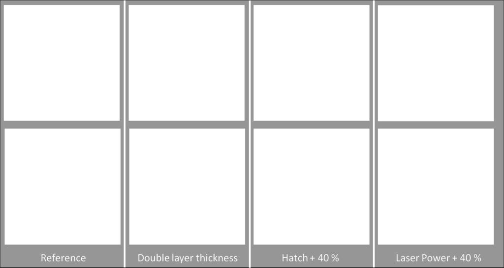
2 Agenda The BIGS Research Project Image Acquisition Setup Application Example: Material Qualification Image Analysis Outlook Dipl.-Ing. Stefan Kleszczynski Dipl.-Ing. 2


3 BIGS Research Project: Objectives Proof of Part Quality and Errors Documentation Understanding Optimization 3


4 BIGS Research Project: Approach Feature Extraction Classifier CCD Camera EOSINT M 270 Part CAD Data Reference Database Reference Image Data Material 4
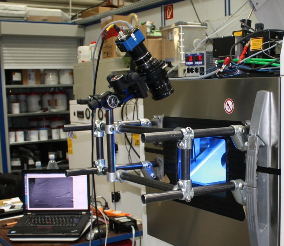
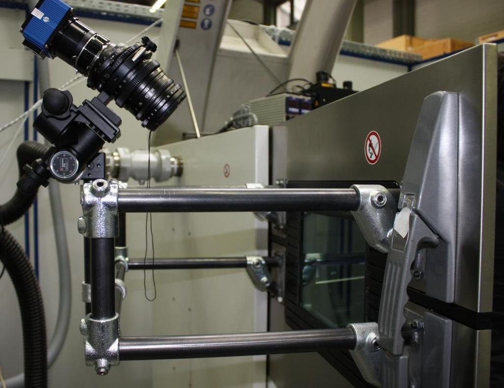
5 Image Acquisition Setup EOS EOSINT M 270 5

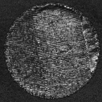
6 29 megapixels Camera Pixel: 5.5 µm x 5.5 µm (sensor: 36 mm x 24 mm) 6

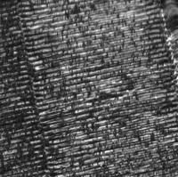
7 Weld Seams: 90 µm 1 pixel: µm 7
8 Application Example: Material Qualification Identification of optimum beam expander position 1 2,5 4 0,5 2 3,5 0 1,5 3 8

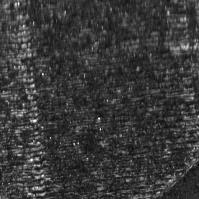
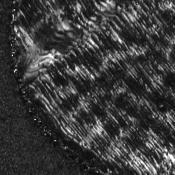
9 Application Example: Material Qualification Poor compound of melt traces Smallest position 4 2 Chosen setting 0 9

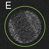
10 Laser Scanning Velocity High Resolution Imaging for DMLS Inspection Application Example: Material Qualification Laser Power A B C D E 10

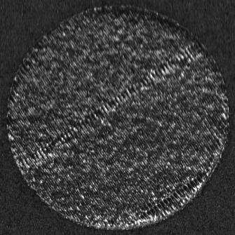
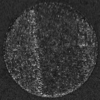
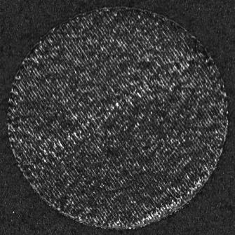
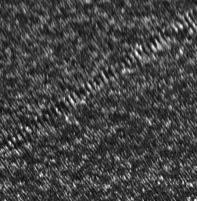
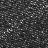
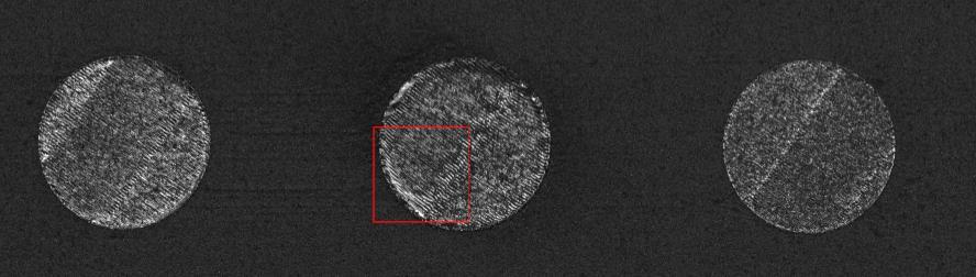
11 Application Example: Material Qualification Hatch 11

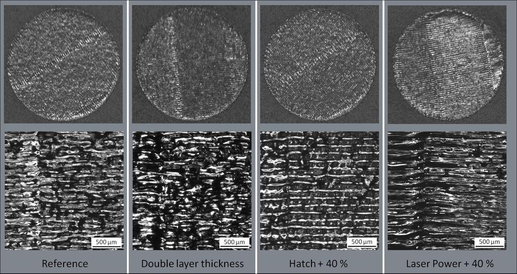
12 Image Analysis: Sample Build +20 % +40 % -20 % -40 % Scanning velocity Laser power Hatch : Increased energy input : Decreased energy input Reference Skip 1 layer 2x exposure Red. overlap 12

13 Impact on Tensile Strength Volume energy density E v : E v = P l h v s d P l : laser power h: hatch distance v s : scanning velocity d: layer thickness Kleszczynski et al. - Mechanical properties of Laser Beam Melting components depending on various process errors 13
14 Microscopic Analysis vs. Imaging System R m = 868 MPa R m = 833 MPa R m = 813 MPa R m = 892 MPa 14
15 Microscopic Analysis vs. Imaging System R m = 868 MPa R m = 833 MPa R m = 813 MPa R m = 892 MPa 15
16 Sample Build: Elevation of Contour Regions Power +40 % Power -40 % 16


17 Sample Build: Elevation of Contour Regions Power +40 % Power -40 % 17


18 Image Analysis: Layer Comparison Manual analysis of multiple layers Synchronized display of selected regions z/mm 18


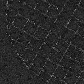
19 Automatic Detection of Differences High Resolution Imaging for DMLS Inspection Texture Analysis
20 Outlook Detection of areas with low energy input Construction of knowledge database, link images to: process parameters part properties 20
21 Summary Inspection of powder and melt result at microscopic scale (weld seams) Existing machines can be equipped with imaging system Images enable analysis of part quality Development of automatic image analysis 21
 zur Jacobsmühlen, J.; Kleszczynski, S.; Schneider, D. & Witt, G. High Resolution Imaging for Inspection of Laser Beam Melting Systems. I2MTC 2013. (to appear) Kleszczynski, S.")
22 References Kleszczynski, S.; zur Jacobsmühlen, J.; Sehrt, J. T. & Witt, G. Mechanical properties of Laser Beam Melting components depending on various process errors. NEW PROLAMAT (to appear) zur Jacobsmühlen, J.; Kleszczynski, S.; Schneider, D. & Witt, G. High Resolution Imaging for Inspection of Laser Beam Melting Systems. I2MTC (to appear) Kleszczynski, S.; zur Jacobsmühlen, J.; Sehrt, J. T. & Witt, G. Error Detection in Laser Beam Melting Systems by High Resolution Imaging. Proc. 23rd Solid Freeform Fabrication Symposium,

23 High Resolution Imaging for DMLS Inspection Contact Details Dipl.-Ing. Stefan Kleszczynski Tel Institute for Product Engineering University of Duisburg-Essen Duisburg, Germany Dipl.-Ing. Tel Institute of Imaging and Computer Vision RWTH Aachen University Aachen, Germany 23
High Resolution Imaging for Inspection of Laser Beam Melting Systems
 High Resolution Imaging for Inspection of Laser Beam Melting Systems a), Stefan Kleszczynski b), Dorian Schneider a), and Gerd Witt b) a) Institute of Imaging and Computer Vision RWTH Aachen University
ERROR DETECTION IN LASER BEAM MELTING SYSTEMS BY HIGH RESOLUTION IMAGING. S. Kleszczynski*, J. zur Jacobsmühlen, J. T. Sehrt* and G.
 ERROR DETECTION IN LASER BEAM MELTING SYSTEMS BY HIGH RESOLUTION IMAGING S. Kleszczynski*, J. zur Jacobsmühlen, J. T. Sehrt* and G. Witt* *Institute for Product Engineering, University of Duisburg-Essen,
IQI-Sensitivity and Applications of Flat Panel Detectors and X-Ray Image Intensifiers A Comparison
 IQI-Sensitivity and Applications of Flat Panel Detectors and X-Ray Image Intensifiers A Comparison Dr. Matthias Purschke/ Ulf Reimer, Agfa NDT Pantak Seifert GmbH und Co. KG, Bogenstr. 4, 96 Ahrensburg,
ORIFICE MEASUREMENT VERISENS APPLICATION DESCRIPTION: REQUIREMENTS APPLICATION CONSIDERATIONS RESOLUTION/ MEASUREMENT ACCURACY. Vision Technologies
 VERISENS APPLICATION DESCRIPTION: ORIFICE MEASUREMENT REQUIREMENTS A major manufacturer of plastic orifices needs to verify that the orifice is within the correct measurement band. Parts are presented
Optical basics for machine vision systems. Lars Fermum Chief instructor STEMMER IMAGING GmbH
 Optical basics for machine vision systems Lars Fermum Chief instructor STEMMER IMAGING GmbH www.stemmer-imaging.de AN INTERNATIONAL CONCEPT STEMMER IMAGING customers in UK Germany France Switzerland Sweden
Information & Instructions
 KEY FEATURES 1. USB 3.0 For the Fastest Transfer Rates Up to 10X faster than regular USB 2.0 connections (also USB 2.0 compatible) 2. High Resolution 4.2 MegaPixels resolution gives accurate profile measurements
Reviewed, accepted August 29, 2003
 ON CERAMIC PARTS FABRICATED RAPID PROTOTYPING MACHINE BASED ON CERAMIC LASER FUSION H. H. Tang*, H. C. Yen*, and W. H. Lin** *Department of Mechanical Engineering, National Taipei University of Technology,
In-process monitoring systems
 White paper In-process monitoring systems for metal additive manufacturing Lukas Fuchs, Christopher Eischer EOS GmbH, Germany Executive summary As additive manufacturing (AM) enters serial production,
Design of an Optical system for the In Situ Process Monitoring of Selective Laser Melting (SLM)
") Available online at www.sciencedirect.com Physics Procedia 12 (2011) 683 690 LiM 2011 Design of an Optical system for the In Situ Process Monitoring of Selective Laser Melting (SLM) Philipp Lott a *, Henrich
Available online at www.sciencedirect.com Physics Procedia 12 (2011) 683 690 LiM 2011 Design of an Optical system for the In Situ Process Monitoring of Selective Laser Melting (SLM) Philipp Lott a *, Henrich
In-Process Sensing of Laser Powder Bed Fusion Additive Manufacturing
 In-Process Sensing of Laser Powder Bed Fusion Additive Manufacturing S. M. Kelly, P.C. Boulware, L. Cronley, G. Firestone, M. Jamshidinia, J. Marchal, T. Stempky, and C. Reichert Presenter: Yu-Ping Yang
OPTIV CLASSIC 321 GL TECHNICAL DATA
 OPTIV CLASSIC 321 GL TECHNICAL DATA TECHNICAL DATA Product description The Optiv Classic 321 GL offers an innovative design for non-contact measurement. The benchtop video-based measuring machine is equipped
Digital Photographic Imaging Using MOEMS
 Digital Photographic Imaging Using MOEMS Vasileios T. Nasis a, R. Andrew Hicks b and Timothy P. Kurzweg a a Department of Electrical and Computer Engineering, Drexel University, Philadelphia, USA b Department
Acuity. Acuity. AP620 Profile Measurement Scanner. Principles of Operation. Definitions. Typical Scanner Applications
 The AP620 profile measurement scanner is s short-range laser scanner for industrial contour and shape measuring applications. The laser profile scanner quickly and accurately generates 2D or 3D profile
In-line measurements of rolling stock macro-geometry
 Optical measuring systems for plate mills Advances in camera technology have enabled a significant enhancement of dimensional measurements in plate mills. Slabs and as-rolled and cut-to-size plates can
DEVELOPMENT CENTER X-RAY TECHNOLOGY EZRT XEYE. Radiation proof X-ray detectors for industrial applications
 DEVELOPMENT CENTER X-RAY TECHNOLOGY EZRT XEYE Radiation proof X-ray detectors for industrial applications The constantly high image quality and long service life of the digital X-ray detectors XEye developed
Applying Automated Optical Inspection Ben Dawson, DALSA Coreco Inc., ipd Group (987)
") Applying Automated Optical Inspection Ben Dawson, DALSA Coreco Inc., ipd Group bdawson@goipd.com (987) 670-2050 Introduction Automated Optical Inspection (AOI) uses lighting, cameras, and vision computers
Applying Automated Optical Inspection Ben Dawson, DALSA Coreco Inc., ipd Group bdawson@goipd.com (987) 670-2050 Introduction Automated Optical Inspection (AOI) uses lighting, cameras, and vision computers
ILLUMINATION AND IMAGE PROCESSING FOR REAL-TIME CONTROL OF DIRECTED ENERGY DEPOSITION ADDITIVE MANUFACTURING
 Solid Freeform Fabrication 2016: Proceedings of the 26th 27th Annual International Solid Freeform Fabrication Symposium An Additive Manufacturing Conference ILLUMINATION AND IMAGE PROCESSING FOR REAL-TIME
Practical Image and Video Processing Using MATLAB
 Practical Image and Video Processing Using MATLAB Chapter 1 Introduction and overview What will we learn? What is image processing? What are the main applications of image processing? What is an image?
Digital Radiography for the Inspection of Small Defects
 ECNDT 2006 - Th.3.2.3 Digital Radiography for the Inspection of Small Defects Bruce Blakeley, TWI, Cambridge, UK Konstantinos Spartiotis, Ajat, Espoo, Finland Abstract. Digital Radiography offers several
Applied Machine Vision
 Applied Machine Vision ME Machine Vision Class Doug Britton GTRI 12/1/2005 Not everybody trusts paintings but people believe photographs. Ansel Adams Machine Vision Components Product Camera/Sensor Illumination
ESCC2006 European Supply Chain Convention
 ESCC2006 European Supply Chain Convention PCB Paper 20 Laser Technology for cutting FPC s and PCB s Mark Hüske, Innovation Manager, LPKF Laser & Electronics AG, Germany Laser Technology for cutting FPCs
ZEISS Axiocam 503 color Your 3 Megapixel Microscope Camera for Fast Image Acquisition Fast, in True Color and Regular Field of View
 Product Information Version 1.0 ZEISS Axiocam 503 color Your 3 Megapixel Microscope Camera for Fast Image Acquisition Fast, in True Color and Regular Field of View ZEISS Axiocam 503 color Sensor Model
products PC Control
 products PC Control 04 2017 PC Control 04 2017 products Image processing directly in the PLC TwinCAT Vision Machine vision easily integrated into automation technology Automatic detection, traceability
Bringing Answers to the Surface
 3D Bringing Answers to the Surface 1 Expanding the Boundaries of Laser Microscopy Measurements and images you can count on. Every time. LEXT OLS4100 Widely used in quality control, research, and development
HORIZON Intelligent cross-linked and flexible process chain
 Intelligent cross-linked and flexible process chain Aachen University enjoys an outstanding reputation and stands for engineering Aachen University Established 1870 40,000 students 10,000 mechanical engineering
SUPRA Optix 3D Optical Profiler
 SUPRA Optix 3D Optical Profiler Scanning White-light Interferometric Microscope SWIM Series Applications The SUPRA Optix is the latest development in the field of Scanning White-light Interferometry. With
Systematic Workflow via Intuitive GUI. Easy operation accomplishes your goals faster than ever.
 Systematic Workflow via Intuitive GUI Easy operation accomplishes your goals faster than ever. 16 With the LEXT OLS4100, observation or measurement begins immediately once the sample is placed on the stage.
1.8.3 Haptic-Based CAD 1.9 About this Book 1.10 Exercises References Development of Additive Manufacturing Technology
 Contents 1 Introduction and Basic Principles 1 1.1 What Is Additive Manufacturing? 1 1.2 What Are AM Parts Used for? 3 1.3 The Generic AM Process 4 1.3.1 Step 1: CAD 4 1.3.2 Step 2: Conversion to STL 4
AxioCam MRc 5 A World of Digital Possibilities
 Microscopy from Carl Zeiss AxioCam MRc 5 A World of Digital Possibilities More flexibility and more performance in microscope camera technology Impressive Performance A trend setter in digital microscopy,
ZEISS Axiocam 512 color Your 12 Megapixel Microscope Camera for Imaging of Large Sample Areas Fast, in True Color, and High Resolution
 Product Information Version 1.0 ZEISS Axiocam 512 color Your 12 Megapixel Microscope Camera for Imaging of Large Sample Areas Fast, in True Color, and High Resolution ZEISS Axiocam 512 color Sensor Model
The Raw Deal Raw VS. JPG
 The Raw Deal Raw VS. JPG Photo Plus Expo New York City, October 31st, 2003. 2003 By Jeff Schewe Notes at: www.schewephoto.com/workshop The Raw Deal How a CCD Works The Chip The Raw Deal How a CCD Works
High Power Dense Spectral Combination Using Commercially Available Lasers and VHGs
 High Power Dense Spectral Combination Using Commercially Available Lasers and VHGs Christophe Moser, CEO Moser@ondax.com Contributors: Gregory Steckman, Frank Havermeyer, Wenhai Liu: Ondax Inc. Christian
OLYMPUS Digital Cameras for Materials Science Applications: Get the Best out of Your Microscope
 Digital Cameras for Microscopy Camera Overview For Materials Science Microscopes OLYMPUS Digital Cameras for Materials Science Applications: Get the Best out of Your Microscope Passionate About Imaging
Overview. About other software. Administrator password. 58. UltraVIEW VoX Getting Started Guide
 Operation 58. UltraVIEW VoX Getting Started Guide Overview This chapter outlines the basic methods used to operate the UltraVIEW VoX system. About other software Volocity places great demands on the computer
METAL LAMINATED TOOLING - A QUICK AND FLEXIBLE TOOLING CONCEPT
 METAL LAMINATED TOOLING - A QUICK AND FLEXIBLE TOOLING CONCEPT Thomas Himmer*, Dr. Anja Techel**, Dr. Steffen Nowotny**, Prof. Dr. Eckhard Beyer**,*** * Fraunhofer USA, Inc., Center for Coatings and Laser
Time Delay Integration (TDI), The Answer to Demands for Increasing Frame Rate/Sensitivity? Craige Palmer Assistant Sales Manager
, The Answer to Demands for Increasing Frame Rate/Sensitivity? Craige Palmer Assistant Sales Manager") Time Delay Integration (TDI), The Answer to Demands for Increasing Frame Rate/Sensitivity? Craige Palmer Assistant Sales Manager Laser Scanning Microscope High Speed Gated PMT Module High Speed Gating
Time Delay Integration (TDI), The Answer to Demands for Increasing Frame Rate/Sensitivity? Craige Palmer Assistant Sales Manager Laser Scanning Microscope High Speed Gated PMT Module High Speed Gating
Beam Shaping and Simultaneous Exposure by Diffractive Optical Element in Laser Plastic Welding
 Beam Shaping and Simultaneous Exposure by Diffractive Optical Element in Laser Plastic Welding AKL`12 9th May 2012 Dr. Daniel Vogler Page 1 Motivation: Quality and flexibility diffractive spot shaping
Basler. Line Scan Cameras
 Basler Line Scan Cameras Next generation CMOS dual line scan technology Up to 140 khz at 2k or 4k resolution, up to 70 khz at 8k resolution Color line scan with 70 khz at 4k resolution High sensitivity
Keywords: Ultrasonic Testing (UT), Air-coupled, Contact-free, Bond, Weld, Composites
, Air-coupled, Contact-free, Bond, Weld, Composites") Single-Sided Contact-Free Ultrasonic Testing A New Air-Coupled Inspection Technology for Weld and Bond Testing M. Kiel, R. Steinhausen, A. Bodi 1, and M. Lucas 1 Research Center for Ultrasonics - Forschungszentrum
Single-Sided Contact-Free Ultrasonic Testing A New Air-Coupled Inspection Technology for Weld and Bond Testing M. Kiel, R. Steinhausen, A. Bodi 1, and M. Lucas 1 Research Center for Ultrasonics - Forschungszentrum
Camera Overview. Digital Microscope Cameras for Material Science: Clear Images, Precise Analysis. Digital Cameras for Microscopy
 Digital Cameras for Microscopy Camera Overview For Materials Science Microscopes Digital Microscope Cameras for Material Science: Clear Images, Precise Analysis Passionate about Imaging: Olympus Digital
Workshop on Network Planning for English speaking African Countries
 Welcome! Workshop on Network Planning for English speaking African Countries (ITU COE, Nairobi, Kenya, 7-11 October 2002) 1 Welcome! Session 5.6 Supporting Network Planning Tools I by Roland Götz 2 Dipl.-Ing.
UV-NIR LASER BEAM PROFILER
 CinCam CCD Technical Data CCD1201 CCD1301 CCD2301 CCD2302 Standard Series Standard Series Standard Series Standard Series SENSOR DATA Format: 1/2 1/3 2/3 2/3 Active area (without cover glass): 6.5mm x
VERSAPRINT 2 The next generation
 VERSAPRINT 2 The next generation The sturdy basic version uses an area camera to align the substrate to the stencil and can use this to carry out optional inspection tasks. The stencil support can be adjusted
Opto-Mechanical Equipment of KBTEM: Present Day and the Future
 KBTEM JSC, Minsk, Belarus Opto-Mechanical Equipment of KBTEM: Present Day and the Future Quality Management System Certificate ISO-9001 since 2001 SPIE Member since 2003 www.kb-omo.by Dr. S.Avakaw SEMI
How does prism technology help to achieve superior color image quality?
 WHITE PAPER How does prism technology help to achieve superior color image quality? Achieving superior image quality requires real and full color depth for every channel, improved color contrast and color
sensicam em electron multiplication digital 12bit CCD camera system
 sensicam em electron multiplication digital 12bit CCD camera system electron multiplication gain of up to 1000 superior resolution (1004 1002 pixel) for EMCCD extremely low noise < 1e excellent quantum
Macro Varon 4.5/85. Key features. Applications. Web and surface inspections
 The Macro Varon lens has been designed for high resolution 12k line scan cameras with 3.5 µm pixel pitch. They are optimized for an optical magnification range of.5x to 2.x. CAS-lens technology produces
Camera Overview. Olympus Digital Cameras for Materials Science Applications: For Clear and Precise Image Analysis. Digital Cameras for Microscopy
 Digital Cameras for Microscopy Camera Overview For Materials Science Microscopes Olympus Digital Cameras for Materials Science Applications: For Clear and Precise Image Analysis Passionate about Imaging
Fig.2: Scanner VistaScan for image plates
 RADIOGRAPHIC INSPECTION OF WELDINGS BY DIGITAL SENSORS H. Thiele, H.-J. Friemel RADIS GmbH, Johanniskirchen, Germany Abstract: The newly available digital sensors for radiographic inspection are suitable
Whitepaper. Open and Flexible: EOS Part Property Management Provides both Individualization and Standardization
 Whitepaper Open and Flexible: EOS Part Property Management Provides both Individualization and Standardization Additive Manufacturing (AM): the Key Technology for e-manufacturing EOS laser sintering solutions
Exercise questions for Machine vision
 Exercise questions for Machine vision This is a collection of exercise questions. These questions are all examination alike which means that similar questions may appear at the written exam. I ve divided
Evaluation of laser-based active thermography for the inspection of optoelectronic devices
 More info about this article: http://www.ndt.net/?id=15849 Evaluation of laser-based active thermography for the inspection of optoelectronic devices by E. Kollorz, M. Boehnel, S. Mohr, W. Holub, U. Hassler
The future of the broadloom inspection
 Contact image sensors realize efficient and economic on-line analysis The future of the broadloom inspection In the printing industry the demands regarding the product quality are constantly increasing.
Examination, TEN1, in courses SK2500/SK2501, Physics of Biomedical Microscopy,
 KTH Applied Physics Examination, TEN1, in courses SK2500/SK2501, Physics of Biomedical Microscopy, 2009-06-05, 8-13, FB51 Allowed aids: Compendium Imaging Physics (handed out) Compendium Light Microscopy
Revisions to ASTM D7310 Standard Guide for Defect Detection and Rating of Plastic Films Using Optical Sensors
 Revisions to ASTM D7310 Standard Guide for Defect Detection and Rating of Plastic Films Using Optical Sensors ANTEC 2017 Brenda Colegrove, The Dow Chemical Company Richard Garner, Borealis Dow.com SPE
Swept-Field User Guide
 Swept-Field User Guide Note: for more details see the Prairie user manual at http://www.prairietechnologies.com/resources/software/prairieview.html Please report any problems to Julie Last (jalast@wisc.edu)
Simulation of Laser Structuring by Three Dimensional Heat Transfer Model
 Simulation of Laser Structuring by Three Dimensional Heat Transfer Model Bassim Bachy, Joerg Franke Abstract In this study, a three dimensional numerical heat transfer model has been used to simulate the
IT FR R TDI CCD Image Sensor
 4k x 4k CCD sensor 4150 User manual v1.0 dtd. August 31, 2015 IT FR 08192 00 R TDI CCD Image Sensor Description: With the IT FR 08192 00 R sensor ANDANTA GmbH builds on and expands its line of proprietary
A NOVEL VISION SYSTEM-ON-CHIP FOR EMBEDDED IMAGE ACQUISITION AND PROCESSING
 A NOVEL VISION SYSTEM-ON-CHIP FOR EMBEDDED IMAGE ACQUISITION AND PROCESSING Neuartiges System-on-Chip für die eingebettete Bilderfassung und -verarbeitung Dr. Jens Döge, Head of Image Acquisition and Processing
MONITORING AND ANALYSIS OF PGMAW. Stefan Nordbruch 1,2 and Axel Gräser 1
 Copyright 2002 IFAC 15th Triennial World Congress, Barcelona, Spain MONITORING AND ANALYSIS OF PGMAW Stefan Nordbruch 1,2 and Axel Gräser 1 1 University Bremen, Institute of Automation Kufsteiner Str.
Dynamic Phase-Shifting Microscopy Tracks Living Cells
 from photonics.com: 04/01/2012 http://www.photonics.com/article.aspx?aid=50654 Dynamic Phase-Shifting Microscopy Tracks Living Cells Dr. Katherine Creath, Goldie Goldstein and Mike Zecchino, 4D Technology
THz-Imaging on its way to industrial application
 THz-Imaging on its way to industrial application T. Pfeifer Laboratory for Machine Tools and Production Engineering (WZL) of RWTH Aachen niversity Manfred-Weck Building, Steinbachstraße 19, D-52074 Aachen,
USING PIV ON THE SPLASH WATER IN A PELTON TURBINE
 USING PIV ON THE SPLASH WATER IN A PELTON TURBINE B.List, J.Prost, H.-B. Matthias Institute for Waterpower and Pumps Vienna University of Technology 1040 Wien, Austria Abstract: At the Institute for Waterpower
Testing Aspheric Lenses: New Approaches
 Nasrin Ghanbari OPTI 521 - Synopsis of a published Paper November 5, 2012 Testing Aspheric Lenses: New Approaches by W. Osten, B. D orband, E. Garbusi, Ch. Pruss, and L. Seifert Published in 2010 Introduction
Background. Computer Vision & Digital Image Processing. Improved Bartlane transmitted image. Example Bartlane transmitted image
 Background Computer Vision & Digital Image Processing Introduction to Digital Image Processing Interest comes from two primary backgrounds Improvement of pictorial information for human perception How
Proposed Adaptive Optics system for Vainu Bappu Telescope
 Proposed Adaptive Optics system for Vainu Bappu Telescope Essential requirements of an adaptive optics system Adaptive Optics is a real time wave front error measurement and correction system The essential
Confocal Raman Microscopy (WITec Alpha 300R)
") Confocal Raman Microscopy (WITec Alpha 300R) Please refer to Witec Alpha300R Confocal Raman Microscope User Manual for the details of the operating procedure. Sample preparation 1. Attach your sample on
Confocal Raman Microscopy (WITec Alpha 300R) Please refer to Witec Alpha300R Confocal Raman Microscope User Manual for the details of the operating procedure. Sample preparation 1. Attach your sample on
The safe & productive robot working without fences
 The European Robot Initiative for Strengthening the Competitiveness of SMEs in Manufacturing The safe & productive robot working without fences Final Presentation, Stuttgart, May 5 th, 2009 Objectives
Camera Overview. Digital Microscope Cameras for Material Science: Clear Images, Precise Analysis. Digital Cameras for Microscopy
 Digital Cameras for Microscopy Camera Overview For Materials Science Microscopes Digital Microscope Cameras for Material Science: Clear Images, Precise Analysis Passionate about Imaging: Olympus Digital
A Turnkey Weld Inspection Solution Combining PAUT & TOFD
 A Turnkey Weld Inspection Solution Combining PAUT & TOFD INTRODUCTION With the recent evolutions of the codes & standards, the replacement of conventional film radiography with advanced ultrasonic testing
Optical Characterization and Defect Inspection for 3D Stacked IC Technology
 Minapad 2014, May 21 22th, Grenoble; France Optical Characterization and Defect Inspection for 3D Stacked IC Technology J.Ph.Piel, G.Fresquet, S.Perrot, Y.Randle, D.Lebellego, S.Petitgrand, G.Ribette FOGALE
System NMI. Accuracy is the Key. Classifying the Content of Non-metallic Inclusions in Steel in Accordance with Current Industrial Standards
 Microscopy from Carl Zeiss System NMI Accuracy is the Key Classifying the Content of Non-metallic Inclusions in Steel in Accordance with Current Industrial Standards New Guidelines Require New Priorities:
Prototypes on demand? Peter Arras De Nayer instituut [Hogeschool voor Wetenschap en Kunst]
![Prototypes on demand? Peter Arras De Nayer instituut [Hogeschool voor Wetenschap en Kunst]](/thumbs/78/77202330.jpg "Prototypes on demand? Peter Arras De Nayer instituut [Hogeschool voor Wetenschap en Kunst]") Prototypes on demand? Peter Arras De Nayer instituut [Hogeschool voor Wetenschap en Kunst] Pressure on time to market urges for new ways of faster prototyping. Key words: Rapid prototyping, rapid tooling,
Prototypes on demand? Peter Arras De Nayer instituut [Hogeschool voor Wetenschap en Kunst] Pressure on time to market urges for new ways of faster prototyping. Key words: Rapid prototyping, rapid tooling,
About EOS. Step 01. Step 02. Step 03
 EOS EOS in Brief About EOS Founded in 1989 and headquartered in Germany, EOS is the technology and market leader for design-driven integrated e-manufacturing solutions for Additive Manufacturing (AM).
The History and Future of Measurement Technology in Sumitomo Electric
 ANALYSIS TECHNOLOGY The History and Future of Measurement Technology in Sumitomo Electric Noritsugu HAMADA This paper looks back on the history of the development of measurement technology that has contributed
Basic design rules for laser sintering. EOS Krailling, 2012
 Basic design rules for laser sintering EOS Krailling, 2012 Useful links for EOS machines, materials and material properties Overview of machines http://www.eos.info/produkte/systeme-zubehoer.html Overview
The end-to-end joining of coils of strip has grown in
 Coil-to-coil joining with laser welding The combination of steel strip edge preparation via laser cutting, accurate strip positioning systems, and laser welding in a single unit provides the optimum coil-to-coil
High-speed Micro-crack Detection of Solar Wafers with Variable Thickness
 High-speed Micro-crack Detection of Solar Wafers with Variable Thickness T. W. Teo, Z. Mahdavipour, M. Z. Abdullah School of Electrical and Electronic Engineering Engineering Campus Universiti Sains Malaysia
Figure 7 Dynamic range expansion of Shack- Hartmann sensor using a spatial-light modulator
 Figure 4 Advantage of having smaller focal spot on CCD with super-fine pixels: Larger focal point compromises the sensitivity, spatial resolution, and accuracy. Figure 1 Typical microlens array for Shack-Hartmann
NELA Brüder Neumeister GmbH
 Vision Inspection Systems NELA Brüder Neumeister GmbH Your Worldwide Partner for Automatic Optical Inspection and Sorting Systems see. control. automate. HISTORICAL MILESTONES 1938 Ernst and Bernhard Neumeister
Laser processing in the medical industry
 Laser processing in the medical industry Laser marking Laser engraving Laser cutting Laser welding Laser digitizing UDI We make your medical devices unique. (01)00001234567890 (10)ACSYS_Medical_2018 (21)29071977
Product Requirements Document: Automated Cosmetic Inspection Machine Optimax
 Product Requirements Document: Automated Cosmetic Inspection Machine Optimax Eric Kwasniewski Aaron Greenbaum Mark Ordway ekwasnie@u.rochester.edu agreenba@u.rochester.edu mordway@u.rochester.edu Customer:
Hochperformante Inline-3D-Messung
 Hochperformante Inline-3D-Messung mittels Lichtfeld Dipl.-Ing. Dorothea Heiss Deputy Head of Business Unit High Performance Image Processing Digital Safety & Security Department AIT Austrian Institute
Measurement technology for inline quality inspection in plastics production. More Precision
 Measurement technology for inline quality inspection in plastics production More Precision Sensors and measurement systems for plastics production Miniaturization and increased production speeds together
Design-Opportunities and Limitations on Additive Manufacturing Determined by a Suitable Test-Specimen
 Design-Opportunities and Limitations on Additive Manufacturing Determined by a Suitable Test-Specimen Karlheinz P.J. Hoeren and Gerd Witt University Duisburg-Essen, Department of Mechanical Engineering,
General functional principle of laser-sintering
 EOS EOS in Brief EOS Technology Additive Manufacturing This technique enables the production of components directly from 3D CAD data. Components are built up layer by layer from materials supplied as fine
X-SCOPE Ultra large FOV micro video colorimeter
 To obtain more information on any of the products below go to our new newsletter page on the website and follow the links, send an email to sales@alrad.co.uk or call 01635 30345. As this is our last newsletter
STEM Spectrum Imaging Tutorial
 STEM Spectrum Imaging Tutorial Gatan, Inc. 5933 Coronado Lane, Pleasanton, CA 94588 Tel: (925) 463-0200 Fax: (925) 463-0204 April 2001 Contents 1 Introduction 1.1 What is Spectrum Imaging? 2 Hardware 3
Pipeline Research Council International, Inc.
 Pipeline Research Council International, Inc. Technology Development for Pipeline Integrity Current Features & Coming Attractions API 2012 Pipeline Conference & Cybernetics Symposium Phoenix, AZ April
High Resolution Sensor Test Comparison with SPOT, KFA1000, KVR1000, IRS-1C and DPA in Lower Saxony
 High Resolution Sensor Test Comparison with SPOT, KFA1000, KVR1000, IRS-1C and DPA in Lower Saxony K. Jacobsen, G. Konecny, H. Wegmann Abstract The Institute for Photogrammetry and Engineering Surveys
Comprehensive GD&T Evaluation Software for Manufacturing Quality Control
 Comprehensive GD&T Evaluation Software for Manufacturing Quality Control Model-Based Family of Software EVOLVE SmartProfile Comprehensive GD&T Evaluation Software for Manufacturing Quality Control Easy
Demo Pattern and Performance Test
 Raith GmbH Hauert 18 Technologiepark D-44227 Dortmund Phone: +49(0)231/97 50 00-0 Fax: +49(0)231/97 50 00-5 Email: postmaster@raith.de Internet: www.raith.com Demo Pattern and Performance Test For Raith
DMLS OF INJECTION MOULD INSERTS FROM 2004 UNTIL TODAY
 DMLS OF INJECTION MOULD INSERTS FROM 2004 UNTIL TODAY LBC LaserBearbeitungsCenter GmbH Im Moldengraben 34 D-70806 Kornwestheim Tel.: 07154/80 88-0 Fax: 07154/80 88-28 E-Mail: Info@LBC-GmbH.de Internet:
3D light microscopy techniques
 3D light microscopy techniques The image of a point is a 3D feature In-focus image Out-of-focus image The image of a point is not a point Point Spread Function (PSF) 1D imaging 1 1 2! NA = 0.5! NA 2D imaging
Student Attendance Monitoring System Via Face Detection and Recognition System
 IJSTE - International Journal of Science Technology & Engineering Volume 2 Issue 11 May 2016 ISSN (online): 2349-784X Student Attendance Monitoring System Via Face Detection and Recognition System Pinal
Practical work no. 3: Confocal Live Cell Microscopy
 Practical work no. 3: Confocal Live Cell Microscopy Course Instructor: Mikko Liljeström (MIU) 1 Background Confocal microscopy: The main idea behind confocality is that it suppresses the signal outside
11Beamage-3. CMOS Beam Profiling Cameras
 11Beamage-3 CMOS Beam Profiling Cameras Key Features USB 3.0 FOR THE FASTEST TRANSFER RATES Up to 10X faster than regular USB 2.0 connections (also USB 2.0 compatible) HIGH RESOLUTION 2.2 MPixels resolution
IN-LAB PELLICLE METROLOGY CHALLENGES
 IN-LAB PELLICLE METROLOGY CHALLENGES Serhiy Danylyuk RWTH Aachen University 04.10.2015, Maastricht Pellicle requirements Pellicle requirem ent HVM Target EUV transmission 90% single pass Spatial non-uniformity
Simple interferometric fringe stabilization by CCD-based feedback control
 Simple interferometric fringe stabilization by CCD-based feedback control Preston P. Young and Purnomo S. Priambodo, Department of Electrical Engineering, University of Texas at Arlington, P.O. Box 19016,
The Mobile CNC Measurement and 3D Scanning System. WENZEL ScanTec MobileScan3D
 The Mobile CNC Measurement and 3D Scanning System WENZEL ScanTec MobileScan3D MobileScan3D What is it and how does it work? MobileScan3D is a truly mobile CNC laser scanning solution allowing fully automatic