Challenges for On-chip Optical Interconnect
|
|
|
- Michael Warren
- 5 years ago
- Views:
Transcription


1 Initial Results of Prototyping a 3-D Integrated Intra-Chip Free-Space Optical Interconnect Berkehan Ciftcioglu, Rebecca Berman, Jian Zhang, Zach Darling, Alok Garg, Jianyun Hu, Manish Jain, Peng Liu, Ioannis Savidis, Shang Wang, Jing Xue, Eby Friedman, Michael Huang, Duncan Moore, Gary Wicks, and Hui Wu Department of Electrical and Computer Engineering The Institute of Optics University of Rochester Challenges for On-chip Optical Interconnect Signaling chain: Efficient Si E/O modulators challenging Inherently poor non-linear optoelectronic properties of Si Resonator designs also non-ideal: e.g., e-beam lithography, temperature stability, insertion loss Off-chip laser (expensive, impractical to power gate) Propagation medium: In-plane waveguides add to the challenge and loss Floor-planning, losses due to crossing, turning, and distance Bandwidth density challenge Density of in-plane wave guide limited WDM: more stringent spectral requirements for devices and higher insertion losses, more expensive laser sources 1
 technology! Large VCSEL arrays, high-density (movable) micro mirrors, high-speed modulators and PDs!")

2 Free-Space Optical Interconnect: an Alternative Optical Domain Electrical Domain Electrical Domain Side view (mirror-guided only) Advantages of Free-Space Optical Interconnect Signaling: mostly current (commercially available) technology! Large VCSEL arrays, high-density (movable) micro mirrors, high-speed modulators and PDs! Integrated VCSELs (Vertical Cavity Surface Emitting Laser) avoids the need for external laser and optical power distribution Disparate technology (e.g., GaAs) Propagation medium! Free-space: low propagation delay, low loss and low dispersion Hindering heat dissipation Networking! Direct communication: relay-free, low overhead, no network deadlock or the necessity to prevent it! Route virtual wires instead of packets New opportunities for system designers! Optimize communication (e.g. cache coherence protocol) 2


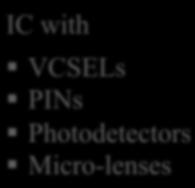
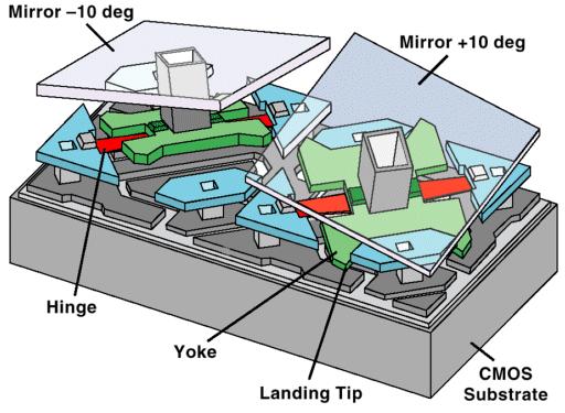
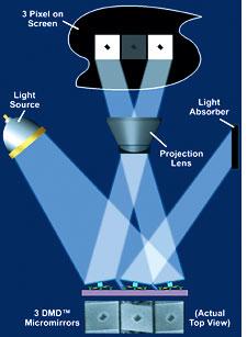
3 Commercially Available Tech. IC with " VCSELs " PINs " Photodetectors " Micro-lenses Digital Micromirror Devices by TI Micro-Optical Electromechanical Device - MOEMS 900,000 microscopic mirrors 3


4 Challenges: Cooling Technologies Cooling using peltier effect - Nextreme the thermal bump at work Graphene Liquid cooling Prototype and Measurement Results 4


5 12/5/10 Link Demo on Board Level Mirror PD VCSEL VCSEL and Microlense Commercial VCSELs Microlenses Divergence: 30 Speed: 10 Gb/s Radius of curvature: 1.22 mm Focal point: 730 µm 5

6 Germanium Photodetector To appear in Photonics Technology Letters Bandwidth: 13 GHz Active Region # Side view of Germanium Photodetector Metal Metal Ti/Au Metal Contacts Anode Cathode Anode Ge substrate Cathode Transmission and Crosstalk Optical path loss Expected = 2.5 db Actual! 6.5 db 6
7 Transmission Losses Due to Beam Clipping PD 1.5dB PD lens 1.25dB VCSEL lens 30 Large divergence angle of the commercial VCSEL VCSEL Small Signal Bandwidth at 1cm Note: Small signal bandwidth does not change with distance 7
8 Summary Fully-distributed free-space optical interconnect provides an alternative Technology readiness Entire signaling chain is commercially available in large scale 3D integration of disparate technologies common in small scale SoCs Thermal issues may be avoided by piggybacking on other developments Initial prototyping results encouraging Initial Results of Prototyping a 3-D Integrated Intra-Chip Free-Space Optical Interconnect Berkehan Ciftcioglu, Rebecca Berman, Jian Zhang, Zach Darling, Alok Garg, Jianyun Hu, Manish Jain, Peng Liu, Ioannis Savidis, Shang Wang, Jing Xue, Eby Friedman, Michael Huang, Duncan Moore, Gary Wicks, and Hui Wu Department of Electrical and Computer Engineering The Institute of Optics University of Rochester 8
 Markers Chemically Wet-etched")
 a) Top")

9 12/5/10 Prototype Custom-Made VCSEL Arrays (20x under microscope) Markers Chemically Wet-etched VCSEL mesas Photograph of VCSEL mesa structure Single VCSEL Structure (Under Microscope) a) Top view of the etched mirrors b) The p-contact region of the VCSEL, located below the mirrors shown in a) 9

 PROCESSOR ICache")
10 Spectrometer Setup 3D Test Chip for System-Level Demo SRAM DCache Transmitter (VCSEL Driver) PROCESSOR ICache Receiver SRAM 10

11 Efficient Optical Links 11
12 Related Work Buffer-less optical packet-switched network, Schacham and Bergman, IEEE Micro 2007 Circuit-switched optical network, Schacham et al. NOC 07 Bus or ring-based shared-medium optical interconnect Ha and Pinkston JPDC 1997 HP Corona (Beausoleil LEOS 2008, Vantrease et al. ISCA 08) Kirman et al. MICRO 06 Free-space optics Miller, J. Sel. Top. in Quantum Elec Krishnamoorthy and Miller, JPDC 1997 Marchand et al. JPDC 1997 Walker et al. Applied Optics
Transmission-Line-Based, Shared-Media On-Chip. Interconnects for Multi-Core Processors
 Design for MOSIS Educational Program (Research) Transmission-Line-Based, Shared-Media On-Chip Interconnects for Multi-Core Processors Prepared by: Professor Hui Wu, Jianyun Hu, Berkehan Ciftcioglu, Jie
The Light at the End of the Wire. Dana Vantrease + HP Labs + Mikko Lipasti
 The Light at the End of the Wire Dana Vantrease + HP Labs + Mikko Lipasti 1 Goals of This Talk Why should we (architects) be interested in optics? How does on-chip optics work? What can we build with optics?
NEXT GENERATION SILICON PHOTONICS FOR COMPUTING AND COMMUNICATION PHILIPPE ABSIL
 NEXT GENERATION SILICON PHOTONICS FOR COMPUTING AND COMMUNICATION PHILIPPE ABSIL OUTLINE Introduction Platform Overview Device Library Overview What s Next? Conclusion OUTLINE Introduction Platform Overview
Electronic-Photonic ICs for Low Cost and Scalable Datacenter Solutions
 Electronic-Photonic ICs for Low Cost and Scalable Datacenter Solutions Christoph Theiss, Director Packaging Christoph.Theiss@sicoya.com 1 SEMICON Europe 2016, October 27 2016 Sicoya Overview Spin-off from
TDM Photonic Network using Deposited Materials
 TDM Photonic Network using Deposited Materials ROBERT HENDRY, GILBERT HENDRY, KEREN BERGMAN LIGHTWAVE RESEARCH LAB COLUMBIA UNIVERSITY HPEC 2011 Motivation for Silicon Photonics Performance scaling becoming
Integrated Focusing Photoresist Microlenses on AlGaAs Top-Emitting VCSELs
 Integrated Focusing Photoresist Microlenses on AlGaAs Top-Emitting VCSELs Andrea Kroner We present 85 nm wavelength top-emitting vertical-cavity surface-emitting lasers (VCSELs) with integrated photoresist
Optical Bus for Intra and Inter-chip Optical Interconnects
 Optical Bus for Intra and Inter-chip Optical Interconnects Xiaolong Wang Omega Optics Inc., Austin, TX Ray T. Chen University of Texas at Austin, Austin, TX Outline Perspective of Optical Backplane Bus
64 Channel Flip-Chip Mounted Selectively Oxidized GaAs VCSEL Array
 64 Channel Flip-Chip Mounted Selectively Oxidized GaAs VCSEL Array 69 64 Channel Flip-Chip Mounted Selectively Oxidized GaAs VCSEL Array Roland Jäger and Christian Jung We have designed and fabricated
IEEE JOURNAL OF SELECTED TOPICS IN QUANTUM ELECTRONICS 2010 Silicon Photonic Circuits: On-CMOS Integration, Fiber Optical Coupling, and Packaging
 IEEE JOURNAL OF SELECTED TOPICS IN QUANTUM ELECTRONICS 2010 Silicon Photonic Circuits: On-CMOS Integration, Fiber Optical Coupling, and Packaging Christophe Kopp, St ephane Bernab e, Badhise Ben Bakir,
Spatial Investigation of Transverse Mode Turn-On Dynamics in VCSELs
 Spatial Investigation of Transverse Mode Turn-On Dynamics in VCSELs Safwat W.Z. Mahmoud Data transmission experiments with single-mode as well as multimode 85 nm VCSELs are carried out from a near-field
Lecture: Integration of silicon photonics with electronics. Prepared by Jean-Marc FEDELI CEA-LETI
 Lecture: Integration of silicon photonics with electronics Prepared by Jean-Marc FEDELI CEA-LETI Context The goal is to give optical functionalities to electronics integrated circuit (EIC) The objectives
Photo-Electronic Crossbar Switching Network for Multiprocessor Systems
 Photo-Electronic Crossbar Switching Network for Multiprocessor Systems Atsushi Iwata, 1 Takeshi Doi, 1 Makoto Nagata, 1 Shin Yokoyama 2 and Masataka Hirose 1,2 1 Department of Physical Electronics Engineering
Low Thermal Resistance Flip-Chip Bonding of 850nm 2-D VCSEL Arrays Capable of 10 Gbit/s/ch Operation
 Low Thermal Resistance Flip-Chip Bonding of 85nm -D VCSEL Arrays Capable of 1 Gbit/s/ch Operation Hendrik Roscher In 3, our well established technology of flip-chip mounted -D 85 nm backside-emitting VCSEL
VERTICAL CAVITY SURFACE EMITTING LASER
 VERTICAL CAVITY SURFACE EMITTING LASER Nandhavel International University Bremen 1/14 Outline Laser action, optical cavity (Fabry Perot, DBR and DBF) What is VCSEL? How does VCSEL work? How is it different
Characterization of Parallel Optical-interconnect Waveguides Integrated on a Printed Circuit Board
 RZ 343 (# 99) 4/12/4 Mathematics & Physics 8 pages Research Report Characterization of Parallel Optical-interconnect Waveguides Integrated on a Printed Circuit Board G.L. Bona, 1 B.J. Offrein, 1 U. Bapst,
Diffraction, Fourier Optics and Imaging
 1 Diffraction, Fourier Optics and Imaging 1.1 INTRODUCTION When wave fields pass through obstacles, their behavior cannot be simply described in terms of rays. For example, when a plane wave passes through
Zukunftstechnologie Dünnglasbasierte elektrooptische. Research Center of Microperipheric Technologies
 Zukunftstechnologie Dünnglasbasierte elektrooptische Baugruppenträger Dr. Henning Schröder Fraunhofer IZM, Berlin, Germany Today/Overview Motivation: external roadmaps High Bandwidth and Channel Density
High-speed free-space based reconfigurable card-to-card optical interconnects with broadcast capability
 High-speed free-space based reconfigurable card-to-card optical interconnects with broadcast capability Ke Wang, 1,2,* Ampalavanapillai Nirmalathas, 1,2 Christina Lim, 2 Efstratios Skafidas, 1,2 and Kamal
PROBE: Prediction-based Optical Bandwidth Scaling for Energy-efficient NoCs
 PROBE: Prediction-based Optical Bandwidth Scaling for Energy-efficient NoCs Li Zhou and Avinash Kodi Technologies for Emerging Computer Architecture Laboratory (TEAL) School of Electrical Engineering and
Index. Cambridge University Press Silicon Photonics Design Lukas Chrostowski and Michael Hochberg. Index.
 absorption, 69 active tuning, 234 alignment, 394 396 apodization, 164 applications, 7 automated optical probe station, 389 397 avalanche detector, 268 back reflection, 164 band structures, 30 bandwidth
Polymer optical waveguide based bi-directional optical bus architecture for high speed optical backplane
 Polymer optical waveguide based bi-directional optical bus architecture for high speed optical backplane Xiaohui Lin a, Xinyuan Dou a, Alan X. Wang b and Ray T. Chen 1,*, Fellow, IEEE a Department of Electrical
Silicon Photonics Photo-Detector Announcement. Mario Paniccia Intel Fellow Director, Photonics Technology Lab
 Silicon Photonics Photo-Detector Announcement Mario Paniccia Intel Fellow Director, Photonics Technology Lab Agenda Intel s Silicon Photonics Research 40G Modulator Recap 40G Photodetector Announcement
A 3.9 ns 8.9 mw 4 4 Silicon Photonic Switch Hybrid-Integrated with CMOS Driver
 A 3.9 ns 8.9 mw 4 4 Silicon Photonic Switch Hybrid-Integrated with CMOS Driver A. Rylyakov, C. Schow, B. Lee, W. Green, J. Van Campenhout, M. Yang, F. Doany, S. Assefa, C. Jahnes, J. Kash, Y. Vlasov IBM
Silicon Photonics in Optical Communications. Lars Zimmermann, IHP, Frankfurt (Oder), Germany
, Germany") Silicon Photonics in Optical Communications Lars Zimmermann, IHP, Frankfurt (Oder), Germany Outline IHP who we are Silicon photonics Photonic-electronic integration IHP photonic technology Conclusions
Silicon Photonics in Optical Communications Lars Zimmermann, IHP, Frankfurt (Oder), Germany Outline IHP who we are Silicon photonics Photonic-electronic integration IHP photonic technology Conclusions
Examination Optoelectronic Communication Technology. April 11, Name: Student ID number: OCT1 1: OCT 2: OCT 3: OCT 4: Total: Grade:
 Examination Optoelectronic Communication Technology April, 26 Name: Student ID number: OCT : OCT 2: OCT 3: OCT 4: Total: Grade: Declaration of Consent I hereby agree to have my exam results published on
Silicon Light Machines Patents
 820 Kifer Road, Sunnyvale, CA 94086 Tel. 408-240-4700 Fax 408-456-0708 www.siliconlight.com Silicon Light Machines Patents USPTO No. US 5,808,797 US 5,841,579 US 5,798,743 US 5,661,592 US 5,629,801 US
Integration of Optoelectronic and RF Devices for Applications in Optical Interconnect and Wireless Communication
 Integration of Optoelectronic and RF Devices for Applications in Optical Interconnect and Wireless Communication Zhaoran (Rena) Huang Assistant Professor Department of Electrical, Computer and System Engineering
Lecture 6 Fiber Optical Communication Lecture 6, Slide 1
 Lecture 6 Optical transmitters Photon processes in light matter interaction Lasers Lasing conditions The rate equations CW operation Modulation response Noise Light emitting diodes (LED) Power Modulation
Fitting Optical Interconnects to an Electrical World- Packaging and Reliability Issues of Arrayed Optoelectronic Modules Keith Goossen, University of
 Fitting Optical Interconnects to an Electrical World- Packaging and Reliability Issues of Arrayed Optoelectronic Modules Keith Goossen, University of Delaware 1 OUTLINE 1. Technology a. Physical rack limitations
4-Channel Optical Parallel Transceiver. Using 3-D Polymer Waveguide
 4-Channel Optical Parallel Transceiver Using 3-D Polymer Waveguide 1 Description Fujitsu Component Limited, in cooperation with Fujitsu Laboratories Ltd., has developed a new bi-directional 4-channel optical
Soft-lithography-based Inter-chip Optical Interconnects
 PIERS ONLINE, VOL. 4, NO. 8, 2008 871 Soft-lithography-based Inter-chip Optical Interconnects Wei Ni 1, Rubing Shao 1, Jing Wu 2, and X. Wu 1 1 State Key Laboratory of Modern Optical Instrumentation, Department
for optical communication system
 High speed Ge waveguide detector for optical communication system Xingjun Wang, Zhijuan Tu and Zhiping Zhou State Key Laboratory of Advanced Optical Communication Systems and Networks, School of Electronics
Investigation of ultrasmall 1 x N AWG for SOI- Based AWG demodulation integration microsystem
 University of Wollongong Research Online Faculty of Engineering and Information Sciences - Papers: Part A Faculty of Engineering and Information Sciences 2015 Investigation of ultrasmall 1 x N AWG for
IST IP NOBEL "Next generation Optical network for Broadband European Leadership"
 DBR Tunable Lasers A variation of the DFB laser is the distributed Bragg reflector (DBR) laser. It operates in a similar manner except that the grating, instead of being etched into the gain medium, is
PARAMETER SYMBOL UNITS MIN TYP MAX TEST CONDITIONS Emission wavelength λ R nm 762,5 763,7 T=25 C, I TEC
 Single Mode VCSEL 763nm TO5 & TEC Vertical Cavity Surface-Emitting Laser internal TEC and Thermistor Narrow linewidth > 2nm tunability with TEC High performance and reliability ELECTRO-OPTICAL CHARACTERISTICS
160-Gb/s Bidirectional Parallel Optical Transceiver Module for Board-Level Interconnects
 160-Gb/s Bidirectional Parallel Optical Transceiver Module for Board-Level Interconnects Fuad Doany, Clint Schow, Jeff Kash C. Baks, D. Kuchta, L. Schares, & R. John IBM T. J. Watson Research Center doany@us.ibm.com
Si CMOS Technical Working Group
 Si CMOS Technical Working Group CTR, Spring 2008 meeting Markets Interconnects TWG Breakouts Reception TWG reports Si CMOS: photonic integration E-P synergy - Integration - Standardization - Cross-market
A Fully Integrated 20 Gb/s Optoelectronic Transceiver Implemented in a Standard
 A Fully Integrated 20 Gb/s Optoelectronic Transceiver Implemented in a Standard 0.13 µm CMOS SOI Technology School of Electrical and Electronic Engineering Yonsei University 이슬아 1. Introduction 2. Architecture
Chapter 1 Introduction
 Chapter 1 Introduction 1-1 Preface Telecommunication lasers have evolved substantially since the introduction of the early AlGaAs-based semiconductor lasers in the late 1970s suitable for transmitting
Micromachined Integrated Optics for Free-Space Interconnections
 Micromachined Integrated Optics for Free-Space Interconnections L. Y. Lin, S. S. Lee, M C. Wu, and K S. J. Pister Electrical Engineering Dept., University of California, Los Angeles, CA 90024, U. S. A.
VCSELs With Enhanced Single-Mode Power and Stabilized Polarization for Oxygen Sensing
 VCSELs With Enhanced Single-Mode Power and Stabilized Polarization for Oxygen Sensing Fernando Rinaldi and Johannes Michael Ostermann Vertical-cavity surface-emitting lasers (VCSELs) with single-mode,
Instruction manual and data sheet ipca h
 1/15 instruction manual ipca-21-05-1000-800-h Instruction manual and data sheet ipca-21-05-1000-800-h Broad area interdigital photoconductive THz antenna with microlens array and hyperhemispherical silicon
Modeling Free Space Optoelectronic Systems Using Ptolemy. Overview
 Modeling Free Space Optoelectronic Systems Using Ptolemy Steven P. Levitan Donald M. Chiarulli Tim P. Kurzweg Mark A. Rempel Departments of Electrical Engineering & Computer Science steve@ee.pitt.edu http://kona.ee.pitt.edu/steve
High-efficiency, high-speed VCSELs with deep oxidation layers
 Manuscript for Review High-efficiency, high-speed VCSELs with deep oxidation layers Journal: Manuscript ID: Manuscript Type: Date Submitted by the Author: Complete List of Authors: Keywords: Electronics
Fabrication of High-Speed Resonant Cavity Enhanced Schottky Photodiodes
 Fabrication of High-Speed Resonant Cavity Enhanced Schottky Photodiodes Abstract We report the fabrication and testing of a GaAs-based high-speed resonant cavity enhanced (RCE) Schottky photodiode. The
A high-speed, tunable silicon photonic ring modulator integrated with ultra-efficient active wavelength control
 A high-speed, tunable silicon photonic ring modulator integrated with ultra-efficient active wavelength control Xuezhe Zheng, 1 Eric Chang, 2 Philip Amberg, 1 Ivan Shubin, 1 Jon Lexau, 2 Frankie Liu, 2
Silicon Photonics Technology Platform To Advance The Development Of Optical Interconnects
 Silicon Photonics Technology Platform To Advance The Development Of Optical Interconnects By Mieke Van Bavel, science editor, imec, Belgium; Joris Van Campenhout, imec, Belgium; Wim Bogaerts, imec s associated
PROGRAMMABLE PHOTONIC ICS:
 PROGRAMMABLE PHOTONIC ICS: MAKING OPTICAL DEVICES MORE VERSATILE Wim Bogaerts PIC International 9-10 April 2018 1 (SILICON) PICS TODAY Rapidly growing integration O(1000) components on a chip photonics
X5 and Z5 Modulator. Telcordia 468. Key Features. Applications. Compliance AGILE OPTICAL COMPONENTS NORTH AMERICA: JDSU (5378)
") AGILE OPTICAL COMPONENTS X5 and Z5 Modulator Key Features Small size: 65 x 12 x 5 mm Surface mountable with gull wing DC pins GPO RF connector Integrated PD (photodiode) for bias and power control 200
AGILE OPTICAL COMPONENTS X5 and Z5 Modulator Key Features Small size: 65 x 12 x 5 mm Surface mountable with gull wing DC pins GPO RF connector Integrated PD (photodiode) for bias and power control 200
Silicon-Photonic Clos Networks for Global On-Chip Communication
 Silicon-Photonic Clos Networks for Global On-Chip Communication Ajay Joshi, Christopher Batten, Yong-Jin Kwon, Scott Beamer, Imran Shamim, Krste Asanović, Vladimir Stojanović NOCS 2009 Massachusetts Institute
MODELING AND EVALUATION OF CHIP-TO-CHIP SCALE SILICON PHOTONIC NETWORKS
 1 MODELING AND EVALUATION OF CHIP-TO-CHIP SCALE SILICON PHOTONIC NETWORKS Robert Hendry, Dessislava Nikolova, Sébastien Rumley, Keren Bergman Columbia University HOTI 2014 2 Chip-to-chip optical networks
NTU RECIPIENTS OF NRF S PROOF OF CONCEPT SCHEME GRANTS. 1. A Semantics-Based and Service-Oriented Framework for the Virtualisation of Sensor Networks
 Reg. No. 200604393R FACT SHEET For immediate release Total: 7 pages including this page Singapore, 21 August 2009 NTU RECIPIENTS OF NRF S PROOF OF CONCEPT SCHEME GRANTS 1. A Semantics-Based and Service-Oriented
PHOTONICS TECHNOLOGY DEVELOPMENT FOR OPTICAL FUZING
 PHOTONICS TECHNOLOGY DEVELOPMENT FOR OPTICAL FUZING Christian M. von der Lippe* U.S. Army Armament Research Development and Engineering Center AMSRD-AAR-AEP-F(A), Adelphi, MD 20783 G. A. Keeler, D. K.
Semiconductor Lasers Semiconductors were originally pumped by lasers or e-beams First diode types developed in 1962: Create a pn junction in
 Semiconductor Lasers Semiconductors were originally pumped by lasers or e-beams First diode types developed in 1962: Create a pn junction in semiconductor material Pumped now with high current density
An 8-Gb/s Optical Backplane Bus Based on Microchannel Interconnects: Design, Fabrication, and Performance Measurements
 JOURNAL OF LIGHTWAVE TECHNOLOGY, VOL. 18, NO. 11, NOVEMBER 2000 1477 An 8-Gb/s Optical Backplane Bus Based on Microchannel Interconnects: Design, Fabrication, and Performance Measurements Gicherl Kim,
inemi OPTOELECTRONICS ROADMAP FOR 2004 Dr. Laura J. Turbini University of Toronto SMTA International September 26, 2005
 inemi OPTOELECTRONICS ROADMAP FOR 2004 0 Dr. Laura J. Turbini University of Toronto SMTA International September 26, 2005 Outline Business Overview Traditional vs Jisso Packaging Levels Optoelectronics
Low-power 2.5 Gbps VCSEL driver in 0.5 µm CMOS technology
 Low-power 2.5 Gbps VCSEL driver in 0.5 µm CMOS technology Bindu Madhavan and A. F. J. Levi Department of Electrical Engineering University of Southern California Los Angeles, California 90089-1111 Indexing
ISSCC 2006 / SESSION 13 / OPTICAL COMMUNICATION / 13.7
 13.7 A 10Gb/s Photonic Modulator and WDM MUX/DEMUX Integrated with Electronics in 0.13µm SOI CMOS Andrew Huang, Cary Gunn, Guo-Liang Li, Yi Liang, Sina Mirsaidi, Adithyaram Narasimha, Thierry Pinguet Luxtera,
Convergence Challenges of Photonics with Electronics
 Convergence Challenges of Photonics with Electronics Edward Palen, Ph.D., P.E. PalenSolutions - Optoelectronic Packaging Consulting www.palensolutions.com palensolutions@earthlink.net 415-850-8166 October
Hybrid vertical-cavity laser integration on silicon
 Invited Paper Hybrid vertical-cavity laser integration on Emanuel P. Haglund* a, Sulakshna Kumari b,c, Johan S. Gustavsson a, Erik Haglund a, Gunther Roelkens b,c, Roel G. Baets b,c, and Anders Larsson
Design and Analysis of Resonant Leaky-mode Broadband Reflectors
 846 PIERS Proceedings, Cambridge, USA, July 6, 8 Design and Analysis of Resonant Leaky-mode Broadband Reflectors M. Shokooh-Saremi and R. Magnusson Department of Electrical and Computer Engineering, University
Compact two-mode (de)multiplexer based on symmetric Y-junction and Multimode interference waveguides
multiplexer based on symmetric Y-junction and Multimode interference waveguides") Compact two-mode (de)multiplexer based on symmetric Y-junction and Multimode interference waveguides Yaming Li, Chong Li, Chuanbo Li, Buwen Cheng, * and Chunlai Xue State Key Laboratory on Integrated Optoelectronics,
Compact two-mode (de)multiplexer based on symmetric Y-junction and Multimode interference waveguides Yaming Li, Chong Li, Chuanbo Li, Buwen Cheng, * and Chunlai Xue State Key Laboratory on Integrated Optoelectronics,
Optical Proximity Communication for a Silicon Photonic Macrochip
 Optical Proximity Communication for a Silicon Photonic Macrochip John E. Cunningham, Ivan Shubin, Xuezhe Zheng, Jon Lexau, Ron Ho, Ying Luo, Guoliang Li, Hiren Thacker, J. Yao, K. Raj and Ashok V. Krishnamoorthy
A Nanophotonic Interconnect for High- Performance Many-Core Computation
 A Nanophotonic Interconnect for High- Performance Many-Core Computation Ray Beausoleil Quantum Optics Research Group Information and Quantum Systems HP Laboratories 008 Hewlett-Packard Development Company,
Polymer Interconnects for Datacom and Sensing. Department of Engineering, University of Cambridge
 Polymer Interconnects for Datacom and Sensing Richard Penty, Ian White, Nikos Bamiedakis, Ying Hao, Fendi Hashim Department of Engineering, University of Cambridge Outline Introduction and Motivation Material
Lecture 12 Building Components
 Optical Fibres and Telecommunications Lecture 12 Building Components Introduction Where are we? Turning individual elements into components Transmitters Receivers Modulation formats Repeaters and 3-R Regeneration
Photonics and Optical Communication
 Photonics and Optical Communication (Course Number 300352) Spring 2007 Dr. Dietmar Knipp Assistant Professor of Electrical Engineering http://www.faculty.iu-bremen.de/dknipp/ 1 Photonics and Optical Communication
Performance Improvement of 40-Gb/s Capacity Four-Channel WDM. Dispersion-Supported Transmission by Using Broadened Passband
 Performance Improvement of 40-Gb/s Capacity Four-Channel WDM Dispersion-Supported Transmission by Using Broadened Passband Arrayed-Waveguide Grating Demultiplexers Mário M. Freire Department of Mathematics
Highly flexible polymeric optical waveguide for out-of-plane optical interconnects
 Highly flexible polymeric optical waveguide for out-of-plane optical interconnects Xinyuan Dou 1, Xiaolong Wang, Xiaohui Lin 1, Duo Ding 1, David Z. Pan 1 and Ray T. Chen 1*, IEEE Fellow 1 Department of
Cavity QED with quantum dots in semiconductor microcavities
 Cavity QED with quantum dots in semiconductor microcavities M. T. Rakher*, S. Strauf, Y. Choi, N.G. Stolz, K.J. Hennessey, H. Kim, A. Badolato, L.A. Coldren, E.L. Hu, P.M. Petroff, D. Bouwmeester University
3550 Aberdeen Ave SE, Kirtland AFB, NM 87117, USA ABSTRACT 1. INTRODUCTION
 Beam Combination of Multiple Vertical External Cavity Surface Emitting Lasers via Volume Bragg Gratings Chunte A. Lu* a, William P. Roach a, Genesh Balakrishnan b, Alexander R. Albrecht b, Jerome V. Moloney
Vertical External Cavity Surface Emitting Laser
 Chapter 4 Optical-pumped Vertical External Cavity Surface Emitting Laser The booming laser techniques named VECSEL combine the flexibility of semiconductor band structure and advantages of solid-state
Flip-Chip Integration of 2-D 850 nm Backside Emitting Vertical Cavity Laser Diode Arrays
 Flip-Chip Integration of 2-D 850 nm Backside Emitting Vertical Cavity Laser Diode Arrays Hendrik Roscher Two-dimensional (2-D) arrays of 850 nm substrate side emitting oxide-confined verticalcavity lasers
3D SOI elements for System-on-Chip applications
 Advanced Materials Research Online: 2011-07-04 ISSN: 1662-8985, Vol. 276, pp 137-144 doi:10.4028/www.scientific.net/amr.276.137 2011 Trans Tech Publications, Switzerland 3D SOI elements for System-on-Chip
3-D Design: Architectures, Methodologies, and Test Circuits
 3-D Design: Architectures, Methodologies, and Test Circuits Eby G. Friedman University of Rochester www.ece.rochester.edu/~friedman June 11, 2010 2 nd Design for 3-D Silicon Integration Workshop 2 Presentation
Mode analysis of Oxide-Confined VCSELs using near-far field approaches
 Annual report 998, Dept. of Optoelectronics, University of Ulm Mode analysis of Oxide-Confined VCSELs using near-far field approaches Safwat William Zaki Mahmoud We analyze the transverse mode structure
Integrated Optoelectronic Chips for Bidirectional Optical Interconnection at Gbit/s Data Rates
 Bidirectional Optical Data Transmission 77 Integrated Optoelectronic Chips for Bidirectional Optical Interconnection at Gbit/s Data Rates Martin Stach and Alexander Kern We report on the fabrication and
SUPPLEMENTARY INFORMATION
 Room-temperature continuous-wave electrically injected InGaN-based laser directly grown on Si Authors: Yi Sun 1,2, Kun Zhou 1, Qian Sun 1 *, Jianping Liu 1, Meixin Feng 1, Zengcheng Li 1, Yu Zhou 1, Liqun
LIGO Photodiode Development and Optical Platform for LIGO Photodetectors Testing
 LIGO Photodiode Development and Optical Platform for LIGO Photodetectors Testing EOPM EOAM PBS EOPM EOAM Ke-Xun Sun Photodiodes --- with Rana Adhikari, Peter Fritschel, Osamu Miyakawa, Allan Weinstein,
A tunable Si CMOS photonic multiplexer/de-multiplexer
 A tunable Si CMOS photonic multiplexer/de-multiplexer OPTICS EXPRESS Published : 25 Feb 2010 MinJae Jung M.I.C.S Content 1. Introduction 2. CMOS photonic 1x4 Si ring multiplexer Principle of add/drop filter
Comparison of Bandwidth Limits for On-card Electrical and Optical Interconnects for 100 Gb/s and Beyond
 Invited Paper Comparison of Bandwidth Limits for On-card Electrical and Optical Interconnects for 1 Gb/s and Beyond Petar Pepeljugoski *, Mark Ritter, Jeffrey A. Kash, Fuad Doany, Clint Schow, Young Kwark,
Improved Output Performance of High-Power VCSELs
 Improved Output Performance of High-Power VCSELs 15 Improved Output Performance of High-Power VCSELs Michael Miller This paper reports on state-of-the-art single device high-power vertical-cavity surfaceemitting
Lecture 22 Optical MEMS (4)
") EEL6935 Advanced MEMS (Spring 2005) Instructor: Dr. Huikai Xie Lecture 22 Optical MEMS (4) Agenda: Refractive Optical Elements Microlenses GRIN Lenses Microprisms Reference: S. Sinzinger and J. Jahns,
EEL6935 Advanced MEMS (Spring 2005) Instructor: Dr. Huikai Xie Lecture 22 Optical MEMS (4) Agenda: Refractive Optical Elements Microlenses GRIN Lenses Microprisms Reference: S. Sinzinger and J. Jahns,
Wavelength-sensitive Thin Film Filter-based Variable Fiber-optic Attenuator with an Embedded Monitoring Port
 Wavelength-sensitive Thin Film Filter-based Variable Fiber-optic Attenuator with an Embedded Monitoring Port Sarun Sumriddetchkajorn and Khunat Chaitavon Electro-Optics Section National Electronics and
EE119 Introduction to Optical Engineering Spring 2003 Final Exam. Name:
 EE119 Introduction to Optical Engineering Spring 2003 Final Exam Name: SID: CLOSED BOOK. THREE 8 1/2 X 11 SHEETS OF NOTES, AND SCIENTIFIC POCKET CALCULATOR PERMITTED. TIME ALLOTTED: 180 MINUTES Fundamental
Department of Microelectronics, Faculty of Electrical Engineering, CTU, Prague Technicka 2, Prague 6, Czech Republic 2
 Ročník 2011 Číslo IV Design and Modeling of the ENR Polymer Microring Resonators Add/Drop Filter for Wavelength Division Multiplexing V. Prajzler 1, E. Strilek 1, I. Huttel 2, J. Spirkova 2, V. Jurka 3
Light source approach for silicon photonics transceivers September Fiber to the Chip
 Light source approach for silicon photonics transceivers September 2014 Fiber to the Chip Silicon Photonics Silicon Photonics Technology: Silicon material system & processing techniques to manufacture
Design Space Exploration of Optical Interfaces for Silicon Photonic Interconnects
 Design Space Exploration of Optical Interfaces for Silicon Photonic Interconnects Olivier Sentieys, Johanna Sepúlveda, Sébastien Le Beux, Jiating Luo, Cedric Killian, Daniel Chillet, Ian O Connor, Hui
ECEN689: Special Topics in Optical Interconnects Circuits and Systems Spring 2016
 ECEN689: Special Topics in Optical Interconnects Circuits and Systems Spring 2016 Lecture 1: Introduction Sam Palermo Analog & Mixed-Signal Center Texas A&M University Class Topics System and design issues
Introduction of 25 Gb/s VCSELs
 Introduction of 25 Gb/s VCSELs IEEE P802.3.ba 40Gb/s and 100Gb/s Ethernet Task Force May 2008, Munich Kenichiro Yashiki - NEC Hikaru Kouta - NEC 1 Contributors and Supporters Jim Tatum - Finisar Akimasa
CHIRPED FIBER BRAGG GRATING (CFBG) BY ETCHING TECHNIQUE FOR SIMULTANEOUS TEMPERATURE AND REFRACTIVE INDEX SENSING
 BY ETCHING TECHNIQUE FOR SIMULTANEOUS TEMPERATURE AND REFRACTIVE INDEX SENSING") CHIRPED FIBER BRAGG GRATING (CFBG) BY ETCHING TECHNIQUE FOR SIMULTANEOUS TEMPERATURE AND REFRACTIVE INDEX SENSING Siti Aisyah bt. Ibrahim and Chong Wu Yi Photonics Research Center Department of Physics,
CHIRPED FIBER BRAGG GRATING (CFBG) BY ETCHING TECHNIQUE FOR SIMULTANEOUS TEMPERATURE AND REFRACTIVE INDEX SENSING Siti Aisyah bt. Ibrahim and Chong Wu Yi Photonics Research Center Department of Physics,
Performance of silicon micro ring modulator with an interleaved p-n junction for optical interconnects
 Indian Journal of Pure & Applied Physics Vol. 55, May 2017, pp. 363-367 Performance of silicon micro ring modulator with an interleaved p-n junction for optical interconnects Priyanka Goyal* & Gurjit Kaur
Fast, Two-Dimensional Optical Beamscanning by Wavelength Switching T. K. Chan, E. Myslivets, J. E. Ford
 Photonics Systems Integration Lab University of California San Diego Jacobs School of Engineering Fast, Two-Dimensional Optical Beamscanning by Wavelength Switching T. K. Chan, E. Myslivets, J. E. Ford
Opportunities and challenges of silicon photonics based System-In-Package
 Opportunities and challenges of silicon photonics based System-In-Package ECTC 2014 Panel session : Emerging Technologies and Market Trends of Silicon Photonics Speaker : Stéphane Bernabé (Leti Photonics
The Development of the 1060 nm 28 Gb/s VCSEL and the Characteristics of the Multi-mode Fiber Link
 Special Issue Optical Communication The Development of the 16 nm 28 Gb/s VCSEL and the Characteristics of the Multi-mode Fiber Link Tomofumi Kise* 1, Toshihito Suzuki* 2, Masaki Funabashi* 1, Kazuya Nagashima*
The Beam Characteristics of High Power Diode Laser Stack
 IOP Conference Series: Materials Science and Engineering PAPER OPEN ACCESS The Beam Characteristics of High Power Diode Laser Stack To cite this article: Yuanyuan Gu et al 2018 IOP Conf. Ser.: Mater. Sci.
IBM T. J. Watson Research Center IBM Corporation
 Broadband Silicon Photonic Switch Integrated with CMOS Drive Electronics B. G. Lee, J. Van Campenhout, A. V. Rylyakov, C. L. Schow, W. M. J. Green, S. Assefa, M. Yang, F. E. Doany, C. V. Jahnes, R. A.
- no emitters/amplifiers available. - complex process - no CMOS-compatible
 Advantages of photonic integrated circuits (PICs) in Microwave Photonics (MWP): compactness low-power consumption, stability flexibility possibility of aggregating optics and electronics functionalities
A 24-Channel 300 Gb/s 8.2 pj/bit Full-Duplex Fiber-Coupled Optical Transceiver Module Based on a Single Holey CMOS IC
 A 24-Channel 300 Gb/s 8.2 pj/bit Full-Duplex Fiber-Coupled Optical Transceiver Module Based on a Single Holey CMOS IC A. Rylyakov, C. Schow, F. Doany, B. Lee, C. Jahnes, Y. Kwark, C.Baks, D. Kuchta, J.
Silicon Photonics: A Platform for Integration, Wafer Level Assembly and Packaging
 Silicon Photonics: A Platform for Integration, Wafer Level Assembly and Packaging M. Asghari Kotura Inc April 27 Contents: Who is Kotura Choice of waveguide technology Challenges and merits of Si photonics