Lecture (06) BJT Amplifiers 3
|
|
|
- Bertram Mills
- 5 years ago
- Views:
Transcription


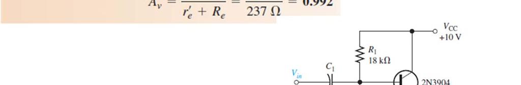
1 Lecture (06) BJT Amplifiers 3 By: Dr. Ahmed ElShafee ١ THE COMMON COLLECTOR AMPLIFIER An emitter follower circuit with voltage divider bias is shown in Figure, the input signal is capacitively coupled to the base, the output signal is capacitively coupled from the emitter, and the collector is at ac ground. There is no phase inversion, the output is approximately the same amplitude as the input ٢

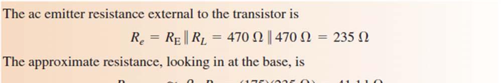
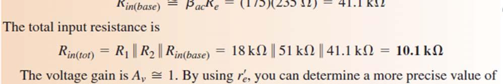
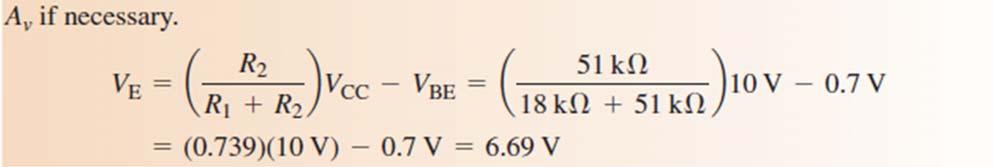
2 gain The capacitive reactances are assumed to be negligible at the frequency of operation. where Re is the parallel combination of RE and RL ٣ If there is no load, then Re RE.. Since the output voltage is at the emitter, it is in phase with the base voltage, so there is no inversion from input to output. Because there is no inversion and because the voltage gain is approximately 1, the output voltage closely follows the input voltage in both phase and amplitude; thus the ٤ term emitter follower.
3 Input Resistance The emitter follower is characterized by a high input resistance; this is what makes it a useful circuit. Because of the high input resistance, it can be used as a buffer to minimize loading effects when a circuit is driving a lowresistance load. ٥ ٦
4 Output Resistance ٧ Current Gain ٨

5 Power Gain ٩ Example 01 ١٠


6 ١١ ١٢


7 ١٣ The Darlington Pair βac is a major factor in determining the input resistance of an amplifier. One way to boost input resistance is to use a Darlington pair ١٤

8 Neglecting r e ١٥ An Application The emitter follower is often used as an interface between a circuit with a high output resistance and a low resistance load. In such an application, the emitterfollower is called a buffer. Suppose a common emitter amplifier with a collector resistance 1k ohm, must drive a low resistance load such as an 8 ohm lowpower speaker. This results in an ac collector resistance of ١٦


9 if the speaker is capacitively coupled to the output of the amplifier, the load appears8 ohm to the ac signal in parallel with the collector resistor. 1k ١٧ An emitter follower using a Darlington pair can be used to interface the amplifier and the speaker, ١٨
")


10 Example 02 ١٩ (a) Determine the voltage gain of the common emitter amplifier ٢٠


 to be The")

11 ٢١ (b) Determine the voltage gain of the Darlington emitterfollower. The effective ac emitter resistance was found in part (a) to be The voltage gain for the Darlington emitter follower is ٢٢
12 (c) Determine the overall voltage gain and compare to the gain of the common emitter amplifier driving the speaker directly without the Darlington emitter follower. ٢٣ The Sziklai Pair The Sziklai pair, is similar to the Darlington pair except that it consists of two types of transistors, an npn and a pnp. known as a complementary Darlington or a compound transistor The current gain is about the same as in the Darlington pair, as illustrated. The difference is that the Q2 base current is the Q1 collector current instead of emitter current, as in the Darlington arrangement. ٢٤
13 An advantage of the Sziklai pair, compared to the Darlington, is that it takes less voltage to turn it on because only one barrier potential has to be overcome. ٢٥ Thanks,.. See you next week (ISA), ٢٦
Lecture (06) BJT Amplifiers 3
 BJT Amplifiers 3") Lecture (06) BJT Amplifiers 3 By: Dr. Ahmed ElShafee 1 Current Gain 2 Power Gain The overall power gain is the product of the overall voltage gain (Av ) and the overall current gain (Ai). 3 THE COMMON
Lecture (06) BJT Amplifiers 3 By: Dr. Ahmed ElShafee 1 Current Gain 2 Power Gain The overall power gain is the product of the overall voltage gain (Av ) and the overall current gain (Ai). 3 THE COMMON
Lecture (05) BJT Amplifiers 2
 BJT Amplifiers 2") Lecture (05) BJT Amplifiers 2 By: Dr. Ahmed ElShafee 1 Effect of the Emitter Bypass Capacitor on Voltage Gain The emitter bypass capacitor, provides an effective short to the ac signal around the emitter
Lecture (05) BJT Amplifiers 2 By: Dr. Ahmed ElShafee 1 Effect of the Emitter Bypass Capacitor on Voltage Gain The emitter bypass capacitor, provides an effective short to the ac signal around the emitter
Lecture (04) BJT Amplifiers 1
 BJT Amplifiers 1") Lecture (04) BJT Amplifiers 1 By: Dr. Ahmed ElShafee ١ The Linear Amplifier A linear amplifier provides amplification of a signal without any distortion so that the output signal A voltage divider biased
Lecture (04) BJT Amplifiers 1 By: Dr. Ahmed ElShafee ١ The Linear Amplifier A linear amplifier provides amplification of a signal without any distortion so that the output signal A voltage divider biased
By: Dr. Ahmed ElShafee
 Lecture (04) Transistor Bias Circuit 3 BJT Amplifiers 1 By: Dr. Ahmed ElShafee ١ Emitter Feedback Bias If an emitter resistor is added to the base bias circuit in Figure, the result is emitter feedback
Electronic Devices. Floyd. Chapter 6. Ninth Edition. Electronic Devices, 9th edition Thomas L. Floyd
 Electronic Devices Ninth Edition Floyd Chapter 6 Agenda BJT AC Analysis Linear Amplifier AC Load Line Transistor AC Model Common Emitter Amplifier Common Collector Amplifier Common Base Amplifier Special
PartIIILectures. Multistage Amplifiers
 University of missan Electronic II, Second year 2015-2016 PartIIILectures Assistant Lecture: 1 Multistage and Compound Amplifiers Basic Definitions: 1- Gain of Multistage Amplifier: Fig.(1-1) A general
Chapter 11 Output Stages
 1 Chapter 11 Output Stages Learning Objectives 2 1) The classification of amplifier output stages 2) Analysis and design of a variety of output-stage types 3) Overview of power amplifiers Introduction
Lecture (10) Power Amplifiers (2)
 Power Amplifiers (2)") Lecture (10) Power Amplifiers (2) By: Dr. Ahmed ElShafee ١ Class B/AB Power the ideal maximum peak output current for both dual supply and single supply push pull amplifiers is approximately Ic(sat), and
Lecture (10) Power Amplifiers (2) By: Dr. Ahmed ElShafee ١ Class B/AB Power the ideal maximum peak output current for both dual supply and single supply push pull amplifiers is approximately Ic(sat), and
Lecture (09) Bipolar Junction Transistor 3
 Bipolar Junction Transistor 3") Lecture (09) Bipolar Junction Transistor 3 By: Dr. Ahmed ElShafee ١ I THE BJT AS AN AMPLIFIER Amplification is the process of linearly increasing the amplitude of an electrical signal and is one of the
Lecture (09) Bipolar Junction Transistor 3 By: Dr. Ahmed ElShafee ١ I THE BJT AS AN AMPLIFIER Amplification is the process of linearly increasing the amplitude of an electrical signal and is one of the
Current Mirrors. Basic BJT Current Mirror. Current mirrors are basic building blocks of analog design. Figure shows the basic NPN current mirror.
 Current Mirrors Basic BJT Current Mirror Current mirrors are basic building blocks of analog design. Figure shows the basic NPN current mirror. For its analysis, we assume identical transistors and neglect
EXPERIMENT 12: SIMULATION STUDY OF DIFFERENT BIASING CIRCUITS USING NPN BJT
 EXPERIMENT 12: SIMULATION STUDY OF DIFFERENT BIASING CIRCUITS USING NPN BJT AIM: 1) To study different BJT DC biasing circuits 2) To design voltage divider bias circuit using NPN BJT SOFTWARE TOOL: PC
Lecture (06) Bipolar Junction Transistor
 Bipolar Junction Transistor") Lecture (06) Bipolar Junction Transistor By: Dr. Ahmed lshafee ١ Agenda BJT structure BJT operation BJT characteristics ٢ BJT structure The BJT is constructed with three doped semiconductor regions One
Lecture (06) Bipolar Junction Transistor By: Dr. Ahmed lshafee ١ Agenda BJT structure BJT operation BJT characteristics ٢ BJT structure The BJT is constructed with three doped semiconductor regions One
Lab 4. Transistor as an amplifier, part 2
 Lab 4 Transistor as an amplifier, part 2 INTRODUCTION We continue the bi-polar transistor experiments begun in the preceding experiment. In the common emitter amplifier experiment, you will learn techniques
... Second Semester
 كنا نظنك اي عيل تركتنا... لكن طيفك مل يزل يغشانا مثل الندى يسقي النبات بقطره... قد ابت ليال يف ادلىج عطشاان ما زلت أذكر حني أدخل معمال... متسك هجازا للقياس تحاكه... فأ راك جتلس هادئا حيرانا تكتب وترمس
Electronic Devices. Floyd. Chapter 7. Ninth Edition. Electronic Devices, 9th edition Thomas L. Floyd
 Electronic Devices Ninth Edition Floyd Chapter 7 Power Amplifiers A power amplifier is a large signal amplifier that produces a replica of the input signal on its output. In the case shown here, the output
Lecture 9 Transistors
 Lecture 9 Transistors Physics Transistor/transistor logic CMOS logic CA 1947 http://www.extremetech.com/extreme/164301-graphenetransistors-based-on-negative-resistance-could-spell-theend-of-silicon-and-semiconductors
Power Amplifiers. Class B Class AB
 ower Amplifiers Class B Class AB Class B he circuit each transistor conducts for a half of every signal period complementary pair push-pull arrangement peration vi ( 0.6; 0.6) (off), (off) v 0 vi v 0.6
Lecture (08) Bipolar Junction Transistor (2)
 Bipolar Junction Transistor (2)") Lecture (08) ipolar Junction Transistor (2) y: Dr. Ahmed lshafee 1 JT haracteristic ollector haracteristic urves 2 Applying fixed V, increasing V Saturation Assume that V is set to produce a certain value
Lecture (08) ipolar Junction Transistor (2) y: Dr. Ahmed lshafee 1 JT haracteristic ollector haracteristic urves 2 Applying fixed V, increasing V Saturation Assume that V is set to produce a certain value
Electronics EECE2412 Spring 2017 Exam #2
 Electronics EECE2412 Spring 2017 Exam #2 Prof. Charles A. DiMarzio Department of Electrical and Computer Engineering Northeastern University 30 March 2017 File:12198/exams/exam2 Name: : General Rules:
EXPERIMENT 5 CURRENT AND VOLTAGE CHARACTERISTICS OF BJT
 EXPERIMENT 5 CURRENT AND VOLTAGE CHARACTERISTICS OF BJT 1. OBJECTIVES 1.1 To practice how to test NPN and PNP transistors using multimeter. 1.2 To demonstrate the relationship between collector current
Transistor Configuration
 Transistor Configuration 1 Objectives To review BJT biasing circuit. To study BJT amplifier circuit To understand the BJT configuration. To analyse single-stage BJT amplifier circuits. To study the differential
Electronic Circuits - Tutorial 07 BJT transistor 1
 Electronic Circuits - Tutorial 07 BJT transistor 1-1 / 20 - T & F # Question 1 A bipolar junction transistor has three terminals. T 2 For operation in the linear or active region, the base-emitter junction
Experiment No. 9 DESIGN AND CHARACTERISTICS OF COMMON BASE AND COMMON COLLECTOR AMPLIFIERS
 Experiment No. 9 DESIGN AND CHARACTERISTICS OF COMMON BASE AND COMMON COLLECTOR AMPLIFIERS 1. Objective: The objective of this experiment is to explore the basic applications of the bipolar junction transistor
Chapter 6: Transistors and Gain
 I. Introduction Chapter 6: Transistors and Gain This week we introduce the transistor. Transistors are three-terminal devices that can amplify a signal and increase the signal s power. The price is that
Electronics Fundamentals BIPOLAR TRANSISTORS. Construction, circuit symbols and biasing examples for NPN and PNP junction transistors.
 IPOLA TANSISTOS onstruction, circuit symbols and biasing examples for NPN and PNP junction transistors Slide 1 xternal bias voltages create an electric field, which pulls electrons (emitted into the base
Well we know that the battery Vcc must be 9V, so that is taken care of.
 HW 4 For the following problems assume a 9Volt battery available. 1. (50 points, BJT CE design) a) Design a common emitter amplifier using a 2N3904 transistor for a voltage gain of Av=-10 with the collector
ESE 372 / Spring 2011 / Lecture 19 Common Base Biased by current source
 ESE 372 / Spring 2011 / Lecture 19 Common Base Biased by current source Output from Collector Start with bias DC analysis make sure BJT is in FA, then calculate small signal parameters for AC analysis.
CHAPTER 3: BIPOLAR JUNCION TRANSISTOR DR. PHẠM NGUYỄN THANH LOAN
 CHAPTER 3: BIPOLAR JUNCION TRANSISTOR DR. PHẠM NGUYỄN THANH LOAN Hanoi, 9/24/2012 Contents 2 Structure and operation of BJT Different configurations of BJT Characteristic curves DC biasing method and analysis
Chapter 3-2 Semiconductor devices Transistors and Amplifiers-BJT Department of Mechanical Engineering
 MEMS1082 Chapter 3-2 Semiconductor devices Transistors and Amplifiers-BJT Bipolar Transistor Construction npn BJT Transistor Structure npn BJT I = I + E C I B V V BE CE = V = V B C V V E E Base-to-emitter
BJT Amplifier Power Amp Overview(H.21)
") BJT Amplifier Power Amp Overview(H.21) 20170616-2 Copyright (c) 2016-2017 Young W. Lim. Permission is granted to copy, distribute and/or modify this document under the terms of the GNU Free Documentation
BJT Amplifier Power Amp Overview(H.21) 20170616-2 Copyright (c) 2016-2017 Young W. Lim. Permission is granted to copy, distribute and/or modify this document under the terms of the GNU Free Documentation
Unit/Standard Number. LEA Task # Alignment
 1 Secondary Competency Task List 100 SAFETY 101 Demonstrate an understanding of State and School safety regulations. 102 Practice safety techniques for electronics work. 103 Demonstrate an understanding
Experiment 6: Biasing Circuitry
 1 Objective UNIVERSITY OF CALIFORNIA AT BERKELEY College of Engineering Department of Electrical Engineering and Computer Sciences EE105 Lab Experiments Experiment 6: Biasing Circuitry Setting up a biasing
Darlington Transistors
 Features: Designed for general-purpose amplifier and low speed switching applications Collector-emitter sustaining voltage - V CEO (sus) = 60 V (minimum) - TIP120, TIP125 80 V (minimum) - TIP121, TIP126
b b Fig. 1 Transistor symbols
 TRANSISTORS Transistors have three terminals which are referred to as emitter (e), base (b) and collector (c). Fig 1 shows the symbols used for the two types of transistors in common use. c c b b e e npn
Lecture 12. Bipolar Junction Transistor (BJT) BJT 1-1
 BJT 1-1") Lecture 12 Bipolar Junction Transistor (BJT) BJT 1-1 Course Info Lecture hours: 4 Two Lectures weekly (Saturdays and Wednesdays) Location: K2 Time: 1:40 pm Tutorial hours: 2 One tutorial class every week
Lecture 12 Bipolar Junction Transistor (BJT) BJT 1-1 Course Info Lecture hours: 4 Two Lectures weekly (Saturdays and Wednesdays) Location: K2 Time: 1:40 pm Tutorial hours: 2 One tutorial class every week
Figure 1. Block diagram of system incorporating power amplification.
 It is often necessary use a circuit which has very low power capabilities to drive a system which has relatively high power requirements. This is typically accomplished by using an amplifier as an intermediate
Last time: BJT CE and CB amplifiers biased by current source
 Last time: BJT CE and CB amplifiers biased by current source Assume FA regime, then VB VC V E I B I E, β 1 I Q C α I, V 0. 7V Calculate V CE and confirm it is > 0.2-0.3V, then BJT can be replaced with
Lecture (03) Diodes and Diode Applications I
 Diodes and Diode Applications I") Lecture (03) Diodes and Diode Applications I By: Dr. Ahmed ElShafee ١ Agenda VOLTAGE CURRENT CHARACTERISTIC OF A DIODE Forward bias Reverse Bias V I Characteristic for Forward Bias V I Characteristic for
Lecture (03) Diodes and Diode Applications I By: Dr. Ahmed ElShafee ١ Agenda VOLTAGE CURRENT CHARACTERISTIC OF A DIODE Forward bias Reverse Bias V I Characteristic for Forward Bias V I Characteristic for
Electronics Prof. D. C. Dube Department of Physics Indian Institute of Technology, Delhi
 Electronics Prof. D. C. Dube Department of Physics Indian Institute of Technology, Delhi Module No # 05 FETS and MOSFETS Lecture No # 06 FET/MOSFET Amplifiers and their Analysis In the previous lecture
Linear electronic. Lecture No. 1
 1 Lecture No. 1 2 3 4 5 Lecture No. 2 6 7 8 9 10 11 Lecture No. 3 12 13 14 Lecture No. 4 Example: find Frequency response analysis for the circuit shown in figure below. Where R S =4kR B1 =8kR B2 =4k R
ANALOG FUNDAMENTALS C. Topic 4 BASIC FET AMPLIFIER CONFIGURATIONS
 AV18-AFC ANALOG FUNDAMENTALS C Topic 4 BASIC FET AMPLIFIER CONFIGURATIONS 1 ANALOG FUNDAMENTALS C AV18-AFC Overview This topic identifies the basic FET amplifier configurations and their principles of
Project (02) Dc 2 AC Inverter
 Dc 2 AC Inverter") Project (02) Dc 2 AC Inverter By: Dr. Ahmed ElShafee 1 12v DC to 220v AC Converter Circuit Using Astable Multivibrator Inverter circuits can either use thyristors as switching devices or transistors. Normally
Project (02) Dc 2 AC Inverter By: Dr. Ahmed ElShafee 1 12v DC to 220v AC Converter Circuit Using Astable Multivibrator Inverter circuits can either use thyristors as switching devices or transistors. Normally
EE 332 Design Project
 EE 332 Design Project Variable Gain Audio Amplifier TA: Pohan Yang Students in the team: George Jenkins Mohamed Logman Dale Jackson Ben Alsin Instructor s Comments: Lab Grade: Introduction The goal of
Tutorial #5: Emitter Follower or Common Collector Amplifier Circuit
 Tutorial #5: Emitter Follower or Common Collector Amplifier Circuit This tutorial will help you to build and simulate a more complex circuit: an emitter follower. The emitter follower or common collector
Electrical, Electronic and Digital Principles (EEDP) Lecture 5. CE Amplifier, Coupling, and Multistage Amplifiers باسم ممدوح الحلوانى
 Lecture 5. CE Amplifier, Coupling, and Multistage Amplifiers باسم ممدوح الحلوانى") Electrical, Electronic and Digital Principles (EEDP) Lecture 5 CE Amplifier, Coupling, and Multistage Amplifiers د. باسم ممدوح الحلوانى Total Output Resistance The output resistance of any system is defined
Electrical, Electronic and Digital Principles (EEDP) Lecture 5 CE Amplifier, Coupling, and Multistage Amplifiers د. باسم ممدوح الحلوانى Total Output Resistance The output resistance of any system is defined
Lecture 12 OUTLINE. Cascode Stage (cont d) Current Mirrors Reading: Chapter 9.2. EE105 Fall 2007 Lecture 12, Slide 1 Prof.
 Current Mirrors Reading: Chapter 9.2. EE105 Fall 2007 Lecture 12, Slide 1 Prof.") Lecture 12 ANNOUNCEMENTS Review session: 3 5PM 5PMFriday (10/5)in 306Soda (HP Auditorium) Midterm #1 (Thursday 10/11, 3:30PM 5:00PM) location: 106 Stanley Hall: Students with last names starting with A
Lecture 12 ANNOUNCEMENTS Review session: 3 5PM 5PMFriday (10/5)in 306Soda (HP Auditorium) Midterm #1 (Thursday 10/11, 3:30PM 5:00PM) location: 106 Stanley Hall: Students with last names starting with A
ESE 319 MT Review
 ESE 319 MT1 2010 Review 1)--> Physical operation of a BJT (layout, why currents are related, npn vs. pnp). 2)Cover the Eber's Mole Model for forward and reverse active configurations. (large signal model)
Experiment 6: Biasing Circuitry
 1 Objective UNIVERSITY OF CALIFORNIA AT BERKELEY College of Engineering Department of Electrical Engineering and Computer Sciences EE105 Lab Experiments Experiment 6: Biasing Circuitry Setting up a biasing
Electrical, Electronic and Communications Engineering Technology/Technician CIP Task Grid
 Secondary Task List 100 SAFETY 101 Describe OSHA safety regulations. 102 Identify, select, and demonstrate proper hand tool use for electronics work. 103 Recognize the types and usages of fire extinguishers.
Bipolar Junction Transistors (BJTs) Overview
 Overview") 1 Bipolar Junction Transistors (BJTs) Asst. Prof. MONTREE SIRIPRUCHYANUN, D. Eng. Dept. of Teacher Training in Electrical Engineering, Faculty of Technical Education King Mongkut s Institute of Technology
1 Bipolar Junction Transistors (BJTs) Asst. Prof. MONTREE SIRIPRUCHYANUN, D. Eng. Dept. of Teacher Training in Electrical Engineering, Faculty of Technical Education King Mongkut s Institute of Technology
ECE 454 Homework #1 Due 11/28/2018 This Wednesday In Lab
 ECE 454 Homework #1 Due 11/28/2018 This Wednesday In Lab Design the Darlington push-pull amplifier specified in Lab 1: You will build this amplifier for Lab 1 so use parts that are available in the lab.
Exercise 2: AC Voltage and Power Gains
 Exercise 2: AC Voltage and Power Gains When you have completed this exercise, you will be able to determine voltage and power gains by using oscilloscope. The ac operation schematic for the COMPLEMENTARY
Microelectronics Circuit Analysis and Design
 Neamen Microelectronics Chapter 6-1 Microelectronics Circuit Analysis and Design Donald A. Neamen Chapter 6 Basic BJT Amplifiers Neamen Microelectronics Chapter 6-2 In this chapter, we will: Understand
Lecture (07) BJT Amplifiers 4 JFET (1)
 BJT Amplifiers 4 JFET (1)") Lecture (07) BJT Amplifiers 4 JFET (1) By: r. Ahmed Elhafee 1 Capacitively Coupled Multistage Amplifier we will use the two stage capacitively coupled amplifier in Figure The output of the first stage
Lecture (07) BJT Amplifiers 4 JFET (1) By: r. Ahmed Elhafee 1 Capacitively Coupled Multistage Amplifier we will use the two stage capacitively coupled amplifier in Figure The output of the first stage
Microelectronics Circuit Analysis and Design. Differential Amplifier Intro. Differential Amplifier Intro. 12/3/2013. In this chapter, we will:
 Microelectronics Circuit Analysis and Design Donald A. Neamen Chapter 11 Differential Amplifiers In this chapter, we will: Describe the characteristics and terminology of the ideal differential amplifier.
Homework Assignment 12
 Homework Assignment 12 Question 1 Shown the is Bode plot of the magnitude of the gain transfer function of a constant GBP amplifier. By how much will the amplifier delay a sine wave with the following
Tutorial 2 BJTs, Transistor Bias Circuits, BJT Amplifiers FETs and FETs Amplifiers. Part 1: BJTs, Transistor Bias Circuits and BJT Amplifiers
 Tutorial 2 BJTs, Transistor Bias Circuits, BJT Amplifiers FETs and FETs Amplifiers Part 1: BJTs, Transistor Bias Circuits and BJT Amplifiers 1. Explain the purpose of a thin, lightly doped base region.
Microelectronics Circuit Analysis and Design. Interdigitated BJT: Top and Cross-Sectional Views. Power Amps 10/11/2013. In this chapter, we will:
 Microelectronics Circuit Analysis and Design Donald A. Neamen Chapter 8 Output Stages and Power Amplifiers In this chapter, we will: Describe the characteristics of BJT and MOSFET power transistors Define
Capacitors, diodes, transistors
 Capacitors, diodes, transistors capacitors charging and time response filters (impedance) semi-conductor diodes rectifiers transformers transistors CHM6158C - Lecture 3 1 Capacitors Symbol 2 Capacitors
TRANSISTOR TRANSISTOR
 It is made up of semiconductor material such as Si and Ge. Usually, it comprises of three terminals namely, base, emitter and collector for providing connection to the external circuit. Today, some transistors
Lecture #3 BJT Transistors & DC Biasing
 November 2014 Ahmad El-Banna Integrated Technical Education Cluster At AlAmeeria J-601-1448 Electronic Principals Lecture #3 BJT Transistors & DC Biasing Instructor: Dr. Ahmad El-Banna Agenda Transistor
ECE 334: Electronic Circuits Lecture 2: BJT Large Signal Model
 Faculty of Engineering ECE 334: Electronic Circuits Lecture 2: BJT Large Signal Model Agenda I & V Notations BJT Devices & Symbols BJT Large Signal Model 2 I, V Notations (1) It is critical to understand
EEE225: Analogue and Digital Electronics
 EEE225: Analogue and Digital Electronics Lecture II James E. Green Department of Electronic Engineering University of Sheffield j.e.green@sheffield.ac.uk This Lecture 1 One Transistor Circuits Continued...
Lecture (03) Diode applications
 Diode applications") Lecture (03) Diode applications By: Dr. Ahmed ElShafee ١ Agenda The Basic DC Power Supply Half wave rectifier Full wave rectifier Filters Voltage Regulators ٢ The Basic DC Power Supply All active electronic
Lecture (03) Diode applications By: Dr. Ahmed ElShafee ١ Agenda The Basic DC Power Supply Half wave rectifier Full wave rectifier Filters Voltage Regulators ٢ The Basic DC Power Supply All active electronic
Midterm 2 Exam. Max: 90 Points
 Midterm 2 Exam Name: Max: 90 Points Question 1 Consider the circuit below. The duty cycle and frequency of the 555 astable is 55% and 5 khz respectively. (a) Determine a value for so that the average current
Revised April Unit/Standard Number. Proficiency Level Achieved: (X) Indicates Competency Achieved to Industry Proficiency Level
 Indicates Competency Achieved to Industry Proficiency Level") Unit/Standard Number Electrical, Electronic and Communications Engineering Technology/Technician CIP 15.0303 Task Grid Secondary Competency Task List 100 SAFETY 101 Demonstrate an understanding of state,
Unit/Standard Number Electrical, Electronic and Communications Engineering Technology/Technician CIP 15.0303 Task Grid Secondary Competency Task List 100 SAFETY 101 Demonstrate an understanding of state,
Electronics EECE2412 Spring 2018 Exam #2
 Electronics EECE2412 Spring 2018 Exam #2 Prof. Charles A. DiMarzio Department of Electrical and Computer Engineering Northeastern University 29 March 2018 File:12262/exams/exam2 Name: General Rules: You
BJT Characteristics & Common Emitter Transistor Amplifier
 LAB #07 Objectives 1. To graph the collector characteristics of a transistor. 2. To measure AC and DC voltages in a common-emitter amplifier. Theory BJT A bipolar (junction) transistor (BJT) is a three-terminal
Transistor Configuration
 Transistor Configuration 1 Objectives To review BJT biasing circuit. To study BJT amplifier circuit To understand the BJT configuration. To analyse single-stage BJT amplifier circuits. To study the differential
By: Dr. Ahmed ElShafee
 Lecture (02) Transistor operating point & DC Load line (2), Transistor Bias Circuit 1 By: Dr. Ahmed ElShafee ١ DC Load Line The dc operation can be described graphically using a dc load line. This is a
ECEN 325 Lab 7: Characterization and DC Biasing of the BJT
 ECEN 325 Lab 7: Characterization and DC Biasing of the BJT 1 Objectives The purpose of this lab is to characterize NPN and PNP bipolar junction transistors (BJT), and to analyze and design DC biasing circuits
Analog Integrated Circuit Configurations
 Analog Integrated Circuit Configurations Basic stages: differential pairs, current biasing, mirrors, etc. Approximate analysis for initial design MOSFET and Bipolar circuits Basic Current Bias Sources
Revised April Unit/Standard Number. High School Graduation Years 2016, 2017 and 2018
 Unit/Standard Number High School Graduation Years 2016, 2017 and 2018 Electrical, Electronic and Communications Engineering Technology/Technician CIP 15.0303 Task Grid Secondary Competency Task List 100
Fundamentals of Microelectronics. Bipolar Amplifier
 Bipolar Amplifier Voltage Amplifier Performance Metrics - There are many metrics that are used to evaluate how good an amplifier is (1) (Voltage) Gain= Vout/ Vin. Can be found from small-signal 10 8 6
Darlington Transistors
 Features: Designed for general-purpose amplifier and low speed switching applications Collector-Emitter sustaining voltage V CEO (sus) = 60 V (Minimum) - TIP45 = 80 V (Minimum) - TIP4, TIP46 = 00 V (Minimum)
ECE 255, Discrete-Circuit Amplifiers
 ECE 255, Discrete-Circuit Amplifiers 20 March 2018 In this lecture, we will continue with the study of transistor amplifiers with the presence of biasing circuits and coupling capacitors in place. We will
ES 330 Electronics II Homework # 2 (Fall 2016 Due Wednesday, September 7, 2016)
") Page1 Name ES 330 Electronics II Homework # 2 (Fall 2016 Due Wednesday, September 7, 2016) Problem 1 (15 points) You are given an NMOS amplifier with drain load resistor R D = 20 k. The DC voltage (V RD
Page1 Name ES 330 Electronics II Homework # 2 (Fall 2016 Due Wednesday, September 7, 2016) Problem 1 (15 points) You are given an NMOS amplifier with drain load resistor R D = 20 k. The DC voltage (V RD
Lab 2: Discrete BJT Op-Amps (Part I)
") Lab 2: Discrete BJT Op-Amps (Part I) This is a three-week laboratory. You are required to write only one lab report for all parts of this experiment. 1.0. INTRODUCTION In this lab, we will introduce and
Lab 2: Discrete BJT Op-Amps (Part I) This is a three-week laboratory. You are required to write only one lab report for all parts of this experiment. 1.0. INTRODUCTION In this lab, we will introduce and
SAMPLE FINAL EXAMINATION FALL TERM
 ENGINEERING SCIENCES 154 ELECTRONIC DEVICES AND CIRCUITS SAMPLE FINAL EXAMINATION FALL TERM 2001-2002 NAME Some Possible Solutions a. Please answer all of the questions in the spaces provided. If you need
The Miller Approximation. CE Frequency Response. The exact analysis is worked out on pp of H&S.
 CE Frequency Response The exact analysis is worked out on pp. 639-64 of H&S. The Miller Approximation Therefore, we consider the effect of C µ on the input node only V ---------- out V s = r g π m ------------------
Electronic Circuits ELCT604 (Spring 2018) Lecture 2 BJT Amplifiers
 Lecture 2 BJT Amplifiers") Electronic Circuits ELCT604 (Spring 2018) Lecture 2 BJT Amplifiers Assistant Professor Office: C3.315 E-mail: eman.azab@guc.edu.eg 1 Analog Voltage Amplifiers Circuit Design and Configurations 2 Objective
Electronic Circuits ELCT604 (Spring 2018) Lecture 2 BJT Amplifiers Assistant Professor Office: C3.315 E-mail: eman.azab@guc.edu.eg 1 Analog Voltage Amplifiers Circuit Design and Configurations 2 Objective
I E I C since I B is very small
 Figure 2: Symbols and nomenclature of a (a) npn and (b) pnp transistor. The BJT consists of three regions, emitter, base, and collector. The emitter and collector are usually of one type of doping, while
Transistors and Applications
 Chapter 17 Transistors and Applications DC Operation of Bipolar Junction Transistors (BJTs) The bipolar junction transistor (BJT) is constructed with three doped semiconductor regions separated by two
Lecture (01) Transistor operating point & DC Load line
 Transistor operating point & DC Load line") Lecture (01) Transistor operating point & DC Load line By: Dr. Ahmed ElShafee ١ BJT Characteristic Collector Characteristic Curves B C E ٢ BJT modes of operation Conditions in Cutoff Conditions in Saturation
Lecture (01) Transistor operating point & DC Load line By: Dr. Ahmed ElShafee ١ BJT Characteristic Collector Characteristic Curves B C E ٢ BJT modes of operation Conditions in Cutoff Conditions in Saturation
Başkent University Department of Electrical and Electronics Engineering EEM 214 Electronics I Experiment 9
 Başkent University Department of Electrical and Electronics Engineering EEM 214 Electronics I Experiment 9 COMMON-COLLECTOR (EMITTER FOLLOWER) AMPLIFIER Aim: 1. To measure the open-circuit voltage gain,
Engineering Spring Homework Assignment 4: BJT Biasing and Small Signal Properties
 Engineering 1620 -- Spring 2011 Homework Assignment 4: BJT Biasing and Small Signal Properties 1.) The circuit below is a common collector amplifier using constant current biasing. (Constant current biasing
4 Transistors. 4.1 IV Relations
 4 Transistors Due date: Sunday, September 19 (midnight) Reading (Bipolar transistors): HH sections 2.01-2.07, (pgs. 62 77) Reading (Field effect transistors) : HH sections 3.01-3.03, 3.11-3.12 (pgs. 113
Audio Amplifier. November 27, 2017
 Audio Amplifier November 27, 2017 1 Pre-lab No pre-lab calculations. 2 Introduction In this lab, you will build an audio power amplifier capable of driving a 8 Ω speaker the way it was meant to be driven...
BDW93C, BDW94C Series
 Features Designed for general-purpose amplifier and low speed switching applications Collector-emitter sustaining voltage- CEO (sus) = (Minimum) Collector-emitter saturation voltage- CE (sat) = 2 (Maximum)
UNIVERSITY OF UTAH ELECTRICAL ENGINEERING DEPARTMENT
 UNIVERSITY OF UTAH ELECTRICAL ENGINEERING DEPARTMENT ECE 3110 LAB EXPERIMENT NO. 4 CLASS AB POWER OUTPUT STAGE Objective: In this laboratory exercise you will build and characterize a class AB power output
Exercise 2: Collector Current Versus Base Current
 Exercise 2: Collector Current Versus Base Current EXERCISE OBJECTIVE When you have completed this exercise, you will be able to demonstrate the relationship of collector current to base current by using
Experiment #6: Biasing an NPN BJT Introduction to CE, CC, and CB Amplifiers
 SCHOOL OF ENGINEERING AND APPLIED SCIENCE DEPARTMENT OF ELECTRICAL AND COMPUTER ENGINEERING ECE 2115: ENGINEERING ELECTRONICS LABORATORY Experiment #6: Biasing an NPN BJT Introduction to CE, CC, and CB
I C I E =I B = I C 1 V BE 0.7 V
 Guide to NPN Amplifier Analysis Jason Woytowich 1. Transistor characteristics A BJT has three operating modes cutoff, active, and saturation. For applications, like amplifiers, where linear characteristics
Course Number Section. Electronics I ELEC 311 BB Examination Date Time # of pages. Final August 12, 2005 Three hours 3 Instructor
 Course Number Section Electronics ELEC 311 BB Examination Date Time # of pages Final August 12, 2005 Three hours 3 nstructor Dr. R. Raut M aterials allowed: No Yes X (Please specify) Calculators allowed:
Electronic Circuits for Mechatronics ELCT 609 Lecture 5: BJT Voltage Amplifiers
 Electronic Circuits for Mechatronics ELCT 609 Lecture 5: BJT Voltage Amplifiers Assistant Professor Office: C3.315 E-mail: eman.azab@guc.edu.eg 1 BJT Modes of Operation Electrical Equations of BJT 2 BJT
Chapter 4 DC Biasing BJTs. BJTs
 hapter 4 D Biasing BJTs BJTs Biasing Biasing: The D voltages applied to a transistor in order to turn it on so that it can amplify the A signal. Operating Point The D input establishes an operating or
Lecture 7. ANNOUNCEMENTS MIDTERM #1 willbe held in class on Thursday, October 11 Review session will be held on Friday, October 5
 Lecture 7 ANNOUNCEMENTS MIDTERM #1 willbe held in class on Thursday, October 11 Review session will be held on Friday, October 5 MIDTERM #2 will be held in class on Tuesday, November 13 OUTLINE BJT Amplifiers
Electronics 1. Lecture 4
 Electronics 1 Lecture 4 Bipolar Junction Transistors. Structure, Characteristics, Basic Circuit Configurations, Biasing Literature 1. Tony R. Kuphaldt: Lessons In Electric Circuits, Volume II AC, 2007
5.25Chapter V Problem Set
 5.25Chapter V Problem Set P5.1 Analyze the circuits in Fig. P5.1 and determine the base, collector, and emitter currents of the BJTs as well as the voltages at the base, collector, and emitter terminals.
Output Stage and Power Amplifiers
 Microelectronic Circuits Output Stage and ower Amplifiers Slide 1 ntroduction Most of the challenging requirement in the design of the output stage is ower delivery to the load. ower consumption at the