Computational Sensors
|
|
|
- Wesley Fletcher
- 5 years ago
- Views:
Transcription


1 Computational Sensors Suren Jayasuriya Postdoctoral Fellow, The Robotics Institute, Carnegie Mellon University
2 Class Announcements 1) Vote on this poll about project checkpoint date on Piazza: 1) Reminder: Start HW5 this first week if you haven t started by Wednesday, you should hurry up.
3 Computational Photography optics to focus light on an image plane digital sensor to capture focused light (electrical process) arbitrary computation between sensor and image Slide courtesy of Ioannis Gkioulekas

4 Computational Photography optics to focus light on an image plane digital sensor to capture focused light (electrical process) arbitrary computation between sensor and image Examples include: Coded Apertures Light Fields Slide courtesy of Ioannis Gkioulekas
5 Computational Photography optics to focus light on an image plane digital sensor to capture focused light (electrical process) arbitrary computation between sensor and image Examples include: Panorama Stitching HDR Imaging Slide courtesy of Ioannis Gkioulekas
6 Computational Photography optics to focus light on an image plane digital sensor to capture focused light (electrical process) arbitrary computation between sensor and image This lecture will cover recent developments in computational sensors Slide courtesy of Ioannis Gkioulekas
7 Review: Traditional CMOS Image Sensors Pixel stack: microlens microlens - Microlens - Color Filter color filter photodiod e potential well color filter photodiod e potential well - Photodiode - Readout Circuitry silicon for readout etc. circuitry stores emitted electrons Slide courtesy of Ioannis Gkioulekas
8 Pixel Diagram and Operation 3T (3 Transistors) Pixel: - Each pixel has a reset, source follower (or amplifier) and row select transistor - The relative timings between turning on/off the transistors = exposure and readout of the pixel

9 Pixel Diagram and Operation RST = ON - The photodiode is charged to a high voltage (between volts for modern technologies)
10 Pixel Diagram and Operation RST = OFF - The photodiode is now integrated photocurrent onto its own (internal) capacitor - Voltage is decreased across the capacitor as (negative) charge accumulates Photocurrent flows from cathode to anode - Eventually, the pixel will saturate or voltage = 0


11 Pixel Diagram and Operation ROW = ON - Transistors Msf and Msel are turned on - The voltage is read out to the column, where it is sent to a column amplifier, then an ADC to be digitized
12 Rolling Shutter CMOS Image Sensor Slide courtesy of Jinwei Gu
13 Image Rows Rolling Shutter Time Slide courtesy of Jinwei Gu
14 Image Rows Rolling Shutter Exposure Time Slide courtesy of Jinwei Gu

15 Image Rows Rolling Shutter Exposure Readout Time Slide courtesy of Jinwei Gu
16 Image Rows Rolling Shutter Exposure Readout Time Slide courtesy of Jinwei Gu
 Disadvantages: - Rolling shutter effect - Can effect performance of computer vision algorithms such as structure-from-motion, SLAM, and stereo if not")
17 Advantages and Disadvantages of Rolling Shutter Advantages: - Easy to read out the image sensor, space-efficient in column parallel readout - No need for extra memory to store pixel voltage (unlike global shutter) Disadvantages: - Rolling shutter effect - Can effect performance of computer vision algorithms such as structure-from-motion, SLAM, and stereo if not careful
 Change the readout/timing (2) Change the pixel design itself (3) Change the on-chip processing optics to focus light on an image plane digital sensor to")
18 Computational Sensors But what is different about computational sensors vs. regular sensors? Some options: (1) Change the readout/timing (2) Change the pixel design itself (3) Change the on-chip processing optics to focus light on an image plane digital sensor to capture focused light (electrical process) arbitrary computation between sensor and image
19 Computational Sensors But what is different about computational sensors vs. regular sensors? Some options: (1) Change the readout/timing (2) Change the pixel design itself CMOS Image Sensor (3) Change the on-chip processing

20 Change the Readout and Timing Gu et al, Coded Rolling Shutter Photography: Flexible Space-Time Sampling ICCP 2010

21 Change the Readout and Timing Gu et al, Coded Rolling Shutter Photography: Flexible Space- Time Sampling ICCP 2010

22 Change the Readout and Timing
23 Computational Sensors But what is different about computational sensors vs. regular sensors? Some options: (1) Change the readout/timing (2) Change the pixel design itself microlens microlens color filter color filter (3) Change the on-chip processing photodiod photodiod e potential well e potential well silicon for readout etc. circuitry stores emitted electrons
24 ASPs: A New Type of Pixel A. Wang and A. Molnar, A Light Field Image Sensor in 180nm CMOS, JSSC 2012
25 Capturing Light Fields using ASPs A. Wang and A. Molnar, A Light Field Image Sensor in 180nm CMOS, JSSC 2012
26 Capturing Light Fields using ASPs n-well Photodiode A. Wang and A. Molnar, A Light Field Image Sensor in 180nm CMOS, JSSC 2012


27 Capturing Light Fields using ASPs n-well Photodiode A. Wang and A. Molnar, A Light Field Image Sensor in 180nm CMOS, JSSC 2012

28 ASPs A. Wang and A. Molnar, A Light Field Image Sensor in 180nm CMOS, JSSC 2012


29 Operating Principle: Talbot Effect Plane wave on grating generates periodic diffraction pattern ~ 1 um 0.5 mm

30 Intensity, a.u. Depth, microns Incident Angle x, microns 10 15


31 Intensity, a.u. Depth, microns Incident Angle shifts x, microns 10 15


32 Add an Analyzer Grating 0 degrees Detector 10 degrees Detector
33 CMOS Implementation Passivation M6 M5 Inter-metal dielectric (SiO 2 ) M4 M3 M2 Interconnect M1 metallization n-well p-substrate
34 Angle Response
35 Angle Response
36 Angle Response
37 Angle Response
38 Angle Response V out = I 0 A θ 1 + m cos βθ + α

39 Quadrature Inversion V 0 = I 0 A θ 1 + m cos βθ V π 2 = I 0 A θ 1 m sin βθ V π = I 0 A θ 1 m cos βθ V 3π 2 = I 0 A θ 1 + m sin βθ Intensity Incident angle I 0 A θ = V 0 + V π 2 = V π 2 + V 3π 2 2 θ = 1 β tan 1 V 0 V π V 3π 2 V π 2
40 2D ASP Tile 10um Physical Layout Impulse Response (2D) Low α 0 γ 0 Low α 0 γ 0 f Med γ 45 Med γ 45 q High α 90 High α 90 ρ α,β,γ (θ) = m 2 cos β cos γ θ x + β sin γ θ y + α

41 ASP Camera We tile the entire image sensor with this repeated pattern of different ASP pixels The sensor is fabricated in an unmodified CMOS process
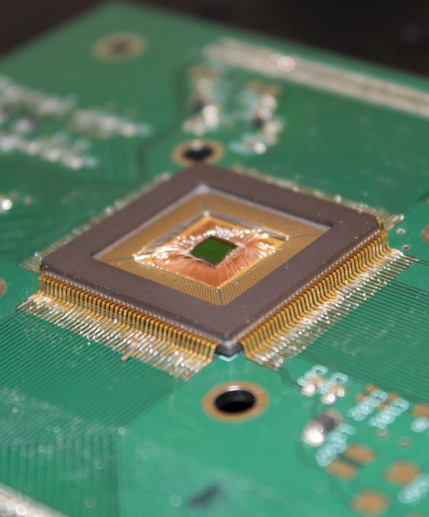
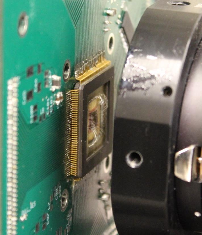

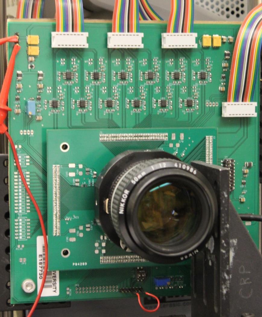
42 Experimental Setup Chip Package Prototype Setup ASP Sensor Main Lens
43 ASP Light Field Capture òò i(x, y) = r (a,b,g ) l(x, y,q,f)dqdf Physical Layout Impulse Response (2D) Each pixel modulates the light field with a different angular response function ρ α,β,γ (θ) = m 2 cos β cos γ θ x + β sin γ θ y + α
44 ASP Light Field Capture Model the image capture process: i = Fl Physical Layout Impulse Response (2D) F ρ α,β,γ (θ) = m 2 cos β cos γ θ x + β sin γ θ y + α
45 ASP Light Field Capture Linear Reconstruction: ldownsampled = F -1 i We can invert this equation using linear methods by reducing the resolution of the 4D light field The resulting reconstruction is low resolution due to the spatio-angular tradeoff
46 Captured 2D Image 4D Light Field Compressive Light Field Photography ASP Projection =

47 Captured 2D Image Compressive Light Field Photography ASP Projection = Overcomplete dictionary Dictionary Sparse Coefficients

48 Decomposing light fields into sparse representations = s.t. is sparse Original Light Field Dictionary Coefficient vector = Overcomplete dictionary Can lead to fewer non-zero coefficients

49 Dictionary Learning Training light fields = s.t. is sparse Use K-SVD algorithm to solve this problem Sample 1,000,000 random 4D patches from training light fields [Marwah et al. 2013]

50 Captured 2D Image Compressive Light Field Reconstruction ASP Projection = Overcomplete dictionary Basis Pursuit Denoise:
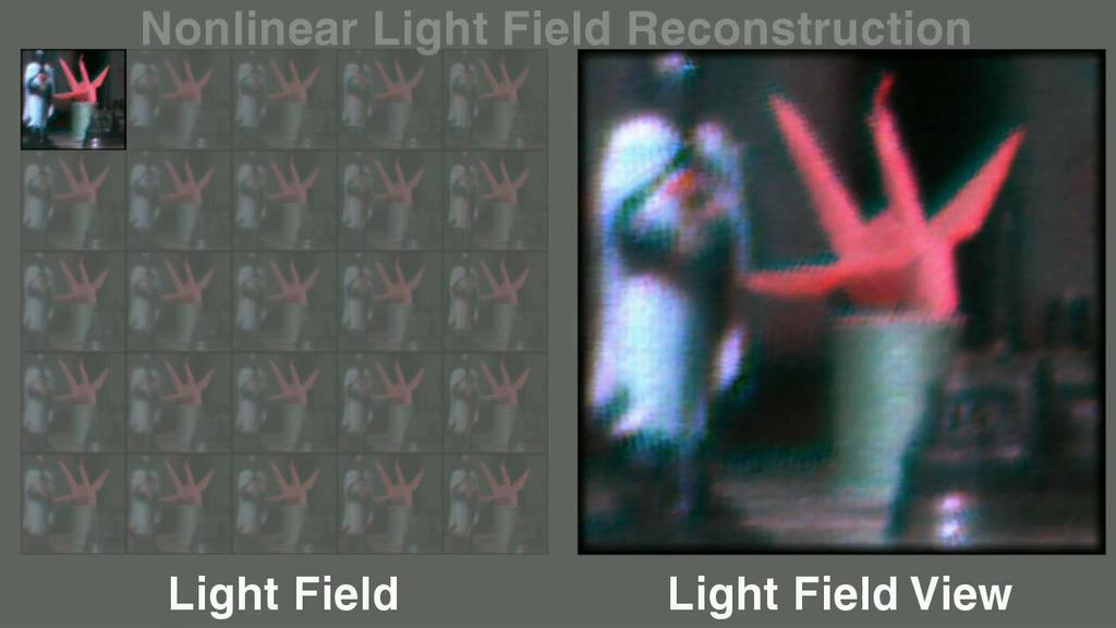
51 Experimental results

52 Comparison of reconstruction methods

53 Digital refocusing after the picture has been taken Focused on Swan Focused on Knight
54 Computational Sensors But what is different about computational sensors vs. regular sensors? Some options: (1) Change the readout/timing (2) Change the pixel design itself microlens microlens color filter color filter (3) Change the on-chip processing photodiod photodiod e potential well e potential well silicon for readout etc. circuitry stores emitted electrons
55 Event-Based Cameras (also called Dynamic Vision Sensors) Dynamic Vision Sensor

56 Event-Based Cameras (also called Dynamic Vision Sensors) Concept Figure for Event Based Camera fhoq High Speed Output on a Quadcopter WTkxM Dynamic Vision Sensor

57 Applications of Event Based Cameras Kim et al, Real-Time 3D Reconstruction and 6-DoF Tracking with an Event Camera ECCV 2016 (Best Paper Award!)

")
58 Time-of-Flight (TOF) Imaging and Transient Imaging Microsoft Kinect V2 Single Photon Avalanche Diodes (SPAD) Streak Cameras
59 Time-of-Flight (TOF) Imaging and Transient Imaging More on TOF and transient imaging in future lectures Single Photon Avalanche Diodes (SPAD) Streak Cameras
 Change the readout/timing (2) Change the pixel design itself (3) Change the on-chip")
60 Computational Sensors But what is different about computational sensors vs. regular sensors? Some options: (1) Change the readout/timing (2) Change the pixel design itself (3) Change the on-chip processing

61 On-Chip Image Compression Chen et al, A CMOS Image Sensor with On-Chip Image Compression Based on Predictive Boundary Adaptation and Memoryless QTD Algorithm, VLSI 2011

62 On-chip CNNs Design of on-chip mixed-signal ADC for implementing a CNN on chip Goal: Energy-efficient computer vision LiKamWa et al, RedEye ISCA 2016
63 Future of Computational Image Sensors Tighter integration of hardware and software, spanning programming languages to computer architecture to circuits to optics Image sensors custom for specific applications (machine vision, scientific imaging, etc) New pixel/sensing technologies: MEMS, Photonics, 3D stacking, etc. What do you predict?
64 References Basic Reading: A El Gamal, H Eltoukhy, CMOS Image Sensors IEEE Circuits and Devices Magazine, 2005 Additional Readings: J. Gu et al, Coded Rolling Shutter Photography: Flexible Space-Time Sampling, ICCP 2010 M. Hirsch et al, A Switchable Light Field Camera Architecture using Angle Sensitive Pixels and Dictionary-based Sparse Coding, ICCP 2014 H. Kim et al, Real-Time 3D Reconstruction and 6-DoF Tracking with an Event Camera ECCV 2016 R. LiKamWa et al., RedEye: Analog ConvNet Image Sensor for Continuous Mobile Vision, ISCA 2016
Fundamentals of CMOS Image Sensors
 CHAPTER 2 Fundamentals of CMOS Image Sensors Mixed-Signal IC Design for Image Sensor 2-1 Outline Photoelectric Effect Photodetectors CMOS Image Sensor(CIS) Array Architecture CIS Peripherals Design Considerations
EE 392B: Course Introduction
 EE 392B Course Introduction About EE392B Goals Topics Schedule Prerequisites Course Overview Digital Imaging System Image Sensor Architectures Nonidealities and Performance Measures Color Imaging Recent
Charged Coupled Device (CCD) S.Vidhya
 S.Vidhya") Charged Coupled Device (CCD) S.Vidhya 02.04.2016 Sensor Physical phenomenon Sensor Measurement Output A sensor is a device that measures a physical quantity and converts it into a signal which can be read
Charged Coupled Device (CCD) S.Vidhya 02.04.2016 Sensor Physical phenomenon Sensor Measurement Output A sensor is a device that measures a physical quantity and converts it into a signal which can be read
Photons and solid state detection
 Photons and solid state detection Photons represent discrete packets ( quanta ) of optical energy Energy is hc/! (h: Planck s constant, c: speed of light,! : wavelength) For solid state detection, photons
Introduction , , Computational Photography Fall 2018, Lecture 1
 Introduction http://graphics.cs.cmu.edu/courses/15-463 15-463, 15-663, 15-862 Computational Photography Fall 2018, Lecture 1 Overview of today s lecture Teaching staff introductions What is computational
A Dynamic Range Expansion Technique for CMOS Image Sensors with Dual Charge Storage in a Pixel and Multiple Sampling
 ensors 2008, 8, 1915-1926 sensors IN 1424-8220 2008 by MDPI www.mdpi.org/sensors Full Research Paper A Dynamic Range Expansion Technique for CMO Image ensors with Dual Charge torage in a Pixel and Multiple
A 3D Multi-Aperture Image Sensor Architecture
 A 3D Multi-Aperture Image Sensor Architecture Keith Fife, Abbas El Gamal and H.-S. Philip Wong Department of Electrical Engineering Stanford University Outline Multi-Aperture system overview Sensor architecture
Image Formation and Capture. Acknowledgment: some figures by B. Curless, E. Hecht, W.J. Smith, B.K.P. Horn, and A. Theuwissen
 Image Formation and Capture Acknowledgment: some figures by B. Curless, E. Hecht, W.J. Smith, B.K.P. Horn, and A. Theuwissen Image Formation and Capture Real world Optics Sensor Devices Sources of Error
Automotive Image Sensors
 Automotive Image Sensors February 1st 2018 Boyd Fowler and Johannes Solhusvik 1 Outline Automotive Image Sensor Market and Applications Viewing Sensors HDR Flicker Mitigation Machine Vision Sensors In
Digital photography , , Computational Photography Fall 2017, Lecture 2
 Digital photography http://graphics.cs.cmu.edu/courses/15-463 15-463, 15-663, 15-862 Computational Photography Fall 2017, Lecture 2 Course announcements To the 14 students who took the course survey on
Colorado School of Mines. Computer Vision. Professor William Hoff Dept of Electrical Engineering &Computer Science.
 Professor William Hoff Dept of Electrical Engineering &Computer Science http://inside.mines.edu/~whoff/ 1 Sensors and Image Formation Imaging sensors and models of image formation Coordinate systems Digital
ABSTRACT. Section I Overview of the µdss
 An Autonomous Low Power High Resolution micro-digital Sun Sensor Ning Xie 1, Albert J.P. Theuwissen 1, 2 1. Delft University of Technology, Delft, the Netherlands; 2. Harvest Imaging, Bree, Belgium; ABSTRACT
Lecture 30: Image Sensors (Cont) Computer Graphics and Imaging UC Berkeley CS184/284A
 Computer Graphics and Imaging UC Berkeley CS184/284A") Lecture 30: Image Sensors (Cont) Computer Graphics and Imaging UC Berkeley Reminder: The Pixel Stack Microlens array Color Filter Anti-Reflection Coating Stack height 4um is typical Pixel size 2um is typical
Lecture 30: Image Sensors (Cont) Computer Graphics and Imaging UC Berkeley Reminder: The Pixel Stack Microlens array Color Filter Anti-Reflection Coating Stack height 4um is typical Pixel size 2um is typical
VLSI DESIGN OF A HIGH-SPEED CMOS IMAGE SENSOR WITH IN-SITU 2D PROGRAMMABLE PROCESSING
 VLSI DESIGN OF A HIGH-SED CMOS IMAGE SENSOR WITH IN-SITU 2D PROGRAMMABLE PROCESSING J.Dubois, D.Ginhac and M.Paindavoine Laboratoire Le2i - UMR CNRS 5158, Universite de Bourgogne Aile des Sciences de l
Digital Photographic Imaging Using MOEMS
 Digital Photographic Imaging Using MOEMS Vasileios T. Nasis a, R. Andrew Hicks b and Timothy P. Kurzweg a a Department of Electrical and Computer Engineering, Drexel University, Philadelphia, USA b Department
Introduction to Computer Vision
 Introduction to Computer Vision CS / ECE 181B Thursday, April 1, 2004 Course Details HW #0 and HW #1 are available. Course web site http://www.ece.ucsb.edu/~manj/cs181b Syllabus, schedule, lecture notes,
Image Formation and Capture
 Figure credits: B. Curless, E. Hecht, W.J. Smith, B.K.P. Horn, A. Theuwissen, and J. Malik Image Formation and Capture COS 429: Computer Vision Image Formation and Capture Real world Optics Sensor Devices
Optical Flow Estimation. Using High Frame Rate Sequences
 Optical Flow Estimation Using High Frame Rate Sequences Suk Hwan Lim and Abbas El Gamal Programmable Digital Camera Project Department of Electrical Engineering, Stanford University, CA 94305, USA ICIP
Image acquisition. In both cases, the digital sensing element is one of the following: Line array Area array. Single sensor
 Image acquisition Digital images are acquired by direct digital acquisition (digital still/video cameras), or scanning material acquired as analog signals (slides, photographs, etc.). In both cases, the
Digital photography , , Computational Photography Fall 2018, Lecture 2
 Digital photography http://graphics.cs.cmu.edu/courses/15-463 15-463, 15-663, 15-862 Computational Photography Fall 2018, Lecture 2 Course announcements To the 26 students who took the start-of-semester
Digital camera. Sensor. Memory card. Circuit board
 Digital camera Circuit board Memory card Sensor Detector element (pixel). Typical size: 2-5 m square Typical number: 5-20M Pixel = Photogate Photon + Thin film electrode (semi-transparent) Depletion volume
A Foveated Visual Tracking Chip
 TP 2.1: A Foveated Visual Tracking Chip Ralph Etienne-Cummings¹, ², Jan Van der Spiegel¹, ³, Paul Mueller¹, Mao-zhu Zhang¹ ¹Corticon Inc., Philadelphia, PA ²Department of Electrical Engineering, Southern
Active Pixel Sensors Fabricated in a Standard 0.18 um CMOS Technology
 Active Pixel Sensors Fabricated in a Standard.18 um CMOS Technology Hui Tian, Xinqiao Liu, SukHwan Lim, Stuart Kleinfelder, and Abbas El Gamal Information Systems Laboratory, Stanford University Stanford,
Detectors for microscopy - CCDs, APDs and PMTs. Antonia Göhler. Nov 2014
 Detectors for microscopy - CCDs, APDs and PMTs Antonia Göhler Nov 2014 Detectors/Sensors in general are devices that detect events or changes in quantities (intensities) and provide a corresponding output,
Opto-VLSI-based reconfigurable photonic RF filter
 Research Online ECU Publications 29 Opto-VLSI-based reconfigurable photonic RF filter Feng Xiao Mingya Shen Budi Juswardy Kamal Alameh This article was originally published as: Xiao, F., Shen, M., Juswardy,
CMOS 0.18 m SPAD. TowerJazz February, 2018 Dr. Amos Fenigstein
 CMOS 0.18 m SPAD TowerJazz February, 2018 Dr. Amos Fenigstein Outline CMOS SPAD motivation Two ended vs. Single Ended SPAD (bulk isolated) P+/N two ended SPAD and its optimization Application of P+/N two
Diode Sensor Lab. Dr. Lynn Fuller
 ROCHESTER INSTITUTE OF TECHNOLOGY MICROELECTRONIC ENGINEERING Diode Sensor Lab Dr. Lynn Fuller Webpage: http://people.rit.edu/lffeee 82 Lomb Memorial Drive Rochester, NY 14623-5604 Tel (585) 475-2035 Fax
Digital Imaging Rochester Institute of Technology
 Digital Imaging 1999 Rochester Institute of Technology So Far... camera AgX film processing image AgX photographic film captures image formed by the optical elements (lens). Unfortunately, the processing
Design and Simulation of High Speed Multi-Processing CMOS Image Sensor
 Design and Simulation of High Speed Multi-Processing CMOS Image Sensor Jérôme Dubois, Dominique Ginhac, Michel Paindavoine Laboratoire LE2I - UMR CNRS 5158 Université de Bourgogne 21078 Dijon Cedex - FRANCE
ECEN474/704: (Analog) VLSI Circuit Design Fall 2016
 VLSI Circuit Design Fall 2016") ECEN474/704: (Analog) VLSI Circuit Design Fall 2016 Lecture 1: Introduction Sam Palermo Analog & Mixed-Signal Center Texas A&M University Announcements Turn in your 0.18um NDA form by Thursday Sep 1 No
ECEN474/704: (Analog) VLSI Circuit Design Fall 2016 Lecture 1: Introduction Sam Palermo Analog & Mixed-Signal Center Texas A&M University Announcements Turn in your 0.18um NDA form by Thursday Sep 1 No
CMOS Today & Tomorrow
 CMOS Today & Tomorrow Uwe Pulsfort TDALSA Product & Application Support Overview Image Sensor Technology Today Typical Architectures Pixel, ADCs & Data Path Image Quality Image Sensor Technology Tomorrow
Lecture Notes 5 CMOS Image Sensor Device and Fabrication
 Lecture Notes 5 CMOS Image Sensor Device and Fabrication CMOS image sensor fabrication technologies Pixel design and layout Imaging performance enhancement techniques Technology scaling, industry trends
Coded photography , , Computational Photography Fall 2017, Lecture 18
 Coded photography http://graphics.cs.cmu.edu/courses/15-463 15-463, 15-663, 15-862 Computational Photography Fall 2017, Lecture 18 Course announcements Homework 5 delayed for Tuesday. - You will need cameras
A 1.3 Megapixel CMOS Imager Designed for Digital Still Cameras
 A 1.3 Megapixel CMOS Imager Designed for Digital Still Cameras Paul Gallagher, Andy Brewster VLSI Vision Ltd. San Jose, CA/USA Abstract VLSI Vision Ltd. has developed the VV6801 color sensor to address
A Framework for Analysis of Computational Imaging Systems
 A Framework for Analysis of Computational Imaging Systems Kaushik Mitra, Oliver Cossairt, Ashok Veeraghavan Rice University Northwestern University Computational imaging CI systems that adds new functionality
The ultimate camera. Computational Photography. Creating the ultimate camera. The ultimate camera. What does it do?
 Computational Photography The ultimate camera What does it do? Image from Durand & Freeman s MIT Course on Computational Photography Today s reading Szeliski Chapter 9 The ultimate camera Infinite resolution
Performance and Characteristics of Silicon Avalanche Photodetectors in
 Performance and Characteristics of Silicon Avalanche Photodetectors in the C5 Process Paper Authors: Dennis Montierth 1, Timothy Strand 2, James Leatham 2, Lloyd Linder 3, and R. Jacob Baker 1 1 Dept.
ELEN6350. Summary: High Dynamic Range Photodetector Hassan Eddrees, Matt Bajor
 ELEN6350 High Dynamic Range Photodetector Hassan Eddrees, Matt Bajor Summary: The use of image sensors presents several limitations for visible light spectrometers. Both CCD and CMOS one dimensional imagers
TRIANGULATION-BASED light projection is a typical
 246 IEEE JOURNAL OF SOLID-STATE CIRCUITS, VOL. 39, NO. 1, JANUARY 2004 A 120 110 Position Sensor With the Capability of Sensitive and Selective Light Detection in Wide Dynamic Range for Robust Active Range
Polarization-analyzing CMOS image sensor with embedded wire-grid polarizers
 Polarization-analyzing CMOS image sensor with embedded wire-grid polarizers Takashi Tokuda, Hirofumi Yamada, Hiroya Shimohata, Kiyotaka, Sasagawa, and Jun Ohta Graduate School of Materials Science, Nara
When Does Computational Imaging Improve Performance?
 When Does Computational Imaging Improve Performance? Oliver Cossairt Assistant Professor Northwestern University Collaborators: Mohit Gupta, Changyin Zhou, Daniel Miau, Shree Nayar (Columbia University)
Putting It All Together: Computer Architecture and the Digital Camera
 461 Putting It All Together: Computer Architecture and the Digital Camera This book covers many topics in circuit analysis and design, so it is only natural to wonder how they all fit together and how
Lecture Notes 10 Image Sensor Optics. Imaging optics. Pixel optics. Microlens
 Lecture Notes 10 Image Sensor Optics Imaging optics Space-invariant model Space-varying model Pixel optics Transmission Vignetting Microlens EE 392B: Image Sensor Optics 10-1 Image Sensor Optics Microlens
Coding and Modulation in Cameras
 Coding and Modulation in Cameras Amit Agrawal June 2010 Mitsubishi Electric Research Labs (MERL) Cambridge, MA, USA Coded Computational Imaging Agrawal, Veeraraghavan, Narasimhan & Mohan Schedule Introduction
IN RECENT years, we have often seen three-dimensional
 622 IEEE JOURNAL OF SOLID-STATE CIRCUITS, VOL. 39, NO. 4, APRIL 2004 Design and Implementation of Real-Time 3-D Image Sensor With 640 480 Pixel Resolution Yusuke Oike, Student Member, IEEE, Makoto Ikeda,
Focal-Plane Compression Imager with Increased Quantization Bit Rate and DPCM Error Modeling
 Focal-Plane Compression Imager with Increased Quantization Bit Rate and DPCM Error Modeling Fernanda Duarte Vilela Reis de Oliveira, Tiago Monnerat de Faria Lopes, José Gabriel Rodríguez Carneiro Gomes,
Charge-integrating organic heterojunction
 In the format provided by the authors and unedited. DOI: 10.1038/NPHOTON.2017.15 Charge-integrating organic heterojunction Wide phototransistors dynamic range for organic wide-dynamic-range heterojunction
Ultra-high resolution 14,400 pixel trilinear color image sensor
 Ultra-high resolution 14,400 pixel trilinear color image sensor Thomas Carducci, Antonio Ciccarelli, Brent Kecskemety Microelectronics Technology Division Eastman Kodak Company, Rochester, New York 14650-2008
Lenses, exposure, and (de)focus
focus") Lenses, exposure, and (de)focus http://graphics.cs.cmu.edu/courses/15-463 15-463, 15-663, 15-862 Computational Photography Fall 2017, Lecture 15 Course announcements Homework 4 is out. - Due October 26
Lenses, exposure, and (de)focus http://graphics.cs.cmu.edu/courses/15-463 15-463, 15-663, 15-862 Computational Photography Fall 2017, Lecture 15 Course announcements Homework 4 is out. - Due October 26
CCDS. Lesson I. Wednesday, August 29, 12
 CCDS Lesson I CCD OPERATION The predecessor of the CCD was a device called the BUCKET BRIGADE DEVICE developed at the Phillips Research Labs The BBD was an analog delay line, made up of capacitors such
Adaptive sensing and image processing with a general-purpose pixel-parallel sensor/processor array integrated circuit
 Adaptive sensing and image processing with a general-purpose pixel-parallel sensor/processor array integrated circuit Piotr Dudek School of Electrical and Electronic Engineering, University of Manchester
Bits From Photons: Oversampled Binary Image Acquisition
 Bits From Photons: Oversampled Binary Image Acquisition Feng Yang Audiovisual Communications Laboratory École Polytechnique Fédérale de Lausanne Thesis supervisor: Prof. Martin Vetterli Thesis co-supervisor:
! Review: MOS IV Curves and Switch Model. ! MOS Device Layout. ! Inverter Layout. ! Gate Layout and Stick Diagrams. ! Design Rules. !
 ESE 570: Digital Integrated Circuits and VLSI Fundamentals Lec 3: January 21, 2017 MOS Fabrication pt. 2: Design Rules and Layout Lecture Outline! Review: MOS IV Curves and Switch Model! MOS Device Layout!
Compressive Imaging. Aswin Sankaranarayanan (Computational Photography Fall 2017)
") Compressive Imaging Aswin Sankaranarayanan (Computational Photography Fall 2017) Traditional Models for Sensing Linear (for the most part) Take as many measurements as unknowns sample Traditional Models
Compressive Imaging Aswin Sankaranarayanan (Computational Photography Fall 2017) Traditional Models for Sensing Linear (for the most part) Take as many measurements as unknowns sample Traditional Models
A Short History of Using Cameras for Weld Monitoring
 A Short History of Using Cameras for Weld Monitoring 2 Background Ever since the development of automated welding, operators have needed to be able to monitor the process to ensure that all parameters
DESIGN OF AN ANALOG FIBER OPTIC TRANSMISSION SYSTEM
 DESIGN OF AN ANALOG FIBER OPTIC TRANSMISSION SYSTEM OBJECTIVE To design and build a complete analog fiber optic transmission system, using light emitting diodes and photodiodes. INTRODUCTION A fiber optic
DIGITAL IMAGING. Handbook of. Wiley VOL 1: IMAGE CAPTURE AND STORAGE. Editor-in- Chief
 Handbook of DIGITAL IMAGING VOL 1: IMAGE CAPTURE AND STORAGE Editor-in- Chief Adjunct Professor of Physics at the Portland State University, Oregon, USA Previously with Eastman Kodak; University of Rochester,
Techniques for Pixel Level Analog to Digital Conversion
 Techniques for Level Analog to Digital Conversion Boyd Fowler, David Yang, and Abbas El Gamal Stanford University Aerosense 98 3360-1 1 Approaches to Integrating ADC with Image Sensor Chip Level Image
1 Introduction & Motivation 1
 Abstract Just five years ago, digital cameras were considered a technological luxury appreciated by only a few, and it was said that digital image quality would always lag behind that of conventional film
A Motion Sensor with On-Chip Pixel Rendering Module for Optical Flow Gradient Extraction
 A Motion Sensor with On-Chip Pixel Rendering Module for Optical Flow Gradient Extraction Jing Huang, Menghan Guo, Shizheng Wang and Shoushun Chen VIRTUS IC Design Centre of Excellence, School of EEE Nanyang
A flexible compact readout circuit for SPAD arrays ABSTRACT Keywords: 1. INTRODUCTION 2. THE SPAD 2.1 Operation 7780C - 55
 A flexible compact readout circuit for SPAD arrays Danial Chitnis * and Steve Collins Department of Engineering Science University of Oxford Oxford England OX13PJ ABSTRACT A compact readout circuit that
A New Single-Photon Avalanche Diode in 90nm Standard CMOS Technology
 A New Single-Photon Avalanche Diode in 90nm Standard CMOS Technology Mohammad Azim Karami* a, Marek Gersbach, Edoardo Charbon a a Dept. of Electrical engineering, Technical University of Delft, Delft,
Photoelectric effect
 Photoelectric effect Objective Study photoelectric effect. Measuring and Calculating Planck s constant, h. Measuring Current-Voltage Characteristics of photoelectric Spectral Lines. Theory Experiments
Low-power smart imagers for vision-enabled wireless sensor networks and a case study
 Low-power smart imagers for vision-enabled wireless sensor networks and a case study J. Fernández-Berni, R. Carmona-Galán, Á. Rodríguez-Vázquez Institute of Microelectronics of Seville (IMSE-CNM), CSIC
Based on lectures by Bernhard Brandl
 Astronomische Waarneemtechnieken (Astronomical Observing Techniques) Based on lectures by Bernhard Brandl Lecture 10: Detectors 2 1. CCD Operation 2. CCD Data Reduction 3. CMOS devices 4. IR Arrays 5.
Design and Implementation of a Scanner with Stitching of Multiple Image Capture
 Y.-W. Bai and C.-C. Cheng: Design and Implementation of a Scanner with Stitching of Multiple Image Capture 1501 Design and Implementation of a Scanner with Stitching of Multiple Image Capture Ying-Wen
A Sorting Image Sensor: An Example of Massively Parallel Intensity to Time Processing for Low Latency Computational Sensors
 Proceedings of the 1996 IEEE International Conference on Robotics and Automation Minneapolis, Minnesota April 1996 A Sorting Image Sensor: An Example of Massively Parallel Intensity to Time Processing
ESE 570: Digital Integrated Circuits and VLSI Fundamentals
 ESE 570: Digital Integrated Circuits and VLSI Fundamentals Lec 3: January 24, 2019 MOS Fabrication pt. 2: Design Rules and Layout Penn ESE 570 Spring 2019 Khanna Jack Keil Wolf Lecture http://www.ese.upenn.edu/about-ese/events/wolf.php
Lecture 1, Introduction and Background
 EE 338L CMOS Analog Integrated Circuit Design Lecture 1, Introduction and Background With the advances of VLSI (very large scale integration) technology, digital signal processing is proliferating and
Camera Image Processing Pipeline
 Lecture 13: Camera Image Processing Pipeline Visual Computing Systems Today (actually all week) Operations that take photons hitting a sensor to a high-quality image Processing systems used to efficiently
A 1Mjot 1040fps 0.22e-rms Stacked BSI Quanta Image Sensor with Cluster-Parallel Readout
 A 1Mjot 1040fps 0.22e-rms Stacked BSI Quanta Image Sensor with Cluster-Parallel Readout IISW 2017 Hiroshima, Japan Saleh Masoodian, Jiaju Ma, Dakota Starkey, Yuichiro Yamashita, Eric R. Fossum May 2017
Device design for global shutter operation in a 1.1-um pixel image sensor and its application to nearinfrared
 Device design for global shutter operation in a 1.1-um pixel image sensor and its application to nearinfrared sensing Zach M. Beiley Robin Cheung Erin F. Hanelt Emanuele Mandelli Jet Meitzner Jae Park
An Introduction to CCDs. The basic principles of CCD Imaging is explained.
 An Introduction to CCDs. The basic principles of CCD Imaging is explained. Morning Brain Teaser What is a CCD? Charge Coupled Devices (CCDs), invented in the 1970s as memory devices. They improved the
Image Formation and Camera Design
 Image Formation and Camera Design Spring 2003 CMSC 426 Jan Neumann 2/20/03 Light is all around us! From London & Upton, Photography Conventional camera design... Ken Kay, 1969 in Light & Film, TimeLife
To Do. Advanced Computer Graphics. Outline. Computational Imaging. How do we see the world? Pinhole camera
 Advanced Computer Graphics CSE 163 [Spring 2017], Lecture 14 Ravi Ramamoorthi http://www.cs.ucsd.edu/~ravir To Do Assignment 2 due May 19 Any last minute issues or questions? Next two lectures: Imaging,
Course Outcome of M.Tech (VLSI Design)
") Course Outcome of M.Tech (VLSI Design) PVL108: Device Physics and Technology The students are able to: 1. Understand the basic physics of semiconductor devices and the basics theory of PN junction. 2.
Course Outcome of M.Tech (VLSI Design) PVL108: Device Physics and Technology The students are able to: 1. Understand the basic physics of semiconductor devices and the basics theory of PN junction. 2.
(12) United States Patent (10) Patent No.: US 7,605,376 B2
 United States Patent (10) Patent No.: US 7,605,376 B2") USOO7605376B2 (12) United States Patent (10) Patent No.: Liu (45) Date of Patent: Oct. 20, 2009 (54) CMOS SENSORADAPTED FOR DENTAL 5,825,033 A * 10/1998 Barrett et al.... 250/370.1 X-RAY MAGING 2007/0069142
USOO7605376B2 (12) United States Patent (10) Patent No.: Liu (45) Date of Patent: Oct. 20, 2009 (54) CMOS SENSORADAPTED FOR DENTAL 5,825,033 A * 10/1998 Barrett et al.... 250/370.1 X-RAY MAGING 2007/0069142
Nano-crystalline Oxide Semiconductor Materials for Semiconductor and Display Technology Sanghun Jeon Ph.D. Associate Professor
 Nano-crystalline Oxide Semiconductor Materials for Semiconductor and Display Technology Sanghun Jeon Ph.D. Associate Professor Department of Applied Physics Korea University Personnel Profile (Affiliation
MICROMACHINED INTERFEROMETER FOR MEMS METROLOGY
 MICROMACHINED INTERFEROMETER FOR MEMS METROLOGY Byungki Kim, H. Ali Razavi, F. Levent Degertekin, Thomas R. Kurfess G.W. Woodruff School of Mechanical Engineering, Georgia Institute of Technology, Atlanta,
Cameras As Computing Systems
 Cameras As Computing Systems Prof. Hank Dietz In Search Of Sensors University of Kentucky Electrical & Computer Engineering Things You Already Know The sensor is some kind of chip Most can't distinguish
Computational Photography Introduction
 Computational Photography Introduction Jongmin Baek CS 478 Lecture Jan 9, 2012 Background Sales of digital cameras surpassed sales of film cameras in 2004. Digital cameras are cool Free film Instant display
Extremely Low-Cost Diagnostic Bio-Sensor using CMOS Technology for Medical Applications
 IOSR Journal of Electronics and Communication Engineering (IOSR-JECE) e-issn: 2278-2834,p- ISSN: 2278-8735.Volume 11, Issue 5, Ver. I (Sep.-Oct.2016), PP 65-72 www.iosrjournals.org Extremely Low-Cost Diagnostic
Deformable MEMS Micromirror Array for Wavelength and Angle Insensitive Retro-Reflecting Modulators Trevor K. Chan & Joseph E. Ford
 Photonics Systems Integration Lab UCSD Jacobs School of Engineering Deformable MEMS Micromirror Array for Wavelength and Angle Insensitive Retro-Reflecting Modulators Trevor K. Chan & Joseph E. Ford PHOTONIC
Spectroscopy in the UV and Visible: Instrumentation. Spectroscopy in the UV and Visible: Instrumentation
 Spectroscopy in the UV and Visible: Instrumentation Typical UV-VIS instrument 1 Source - Disperser Sample (Blank) Detector Readout Monitor the relative response of the sample signal to the blank Transmittance
MEGAFRAME: a fully integrated, timeresolved SPAD pixel array with microconcentrators
 MEGAFRAME: a fully integrated, timeresolved 160 128 SPAD pixel array with microconcentrators J. Arlt 5, F. Borghetti 4, C. E. Bruschini 1, E. Charbon 1,6, D. T. F. Dryden 5, S. East 3, M. W. Fishburn 6,
Deconvolution , , Computational Photography Fall 2018, Lecture 12
 Deconvolution http://graphics.cs.cmu.edu/courses/15-463 15-463, 15-663, 15-862 Computational Photography Fall 2018, Lecture 12 Course announcements Homework 3 is out. - Due October 12 th. - Any questions?
A CMOS Imager with PFM/PWM Based Analogto-digital
 Edith Cowan University Research Online ECU Publications Pre. 2011 2002 A CMOS Imager with PFM/PWM Based Analogto-digital Converter Amine Bermak Edith Cowan University 10.1109/ISCAS.2002.1010386 This conference
White Paper High Dynamic Range Imaging
 WPE-2015XI30-00 for Machine Vision What is Dynamic Range? Dynamic Range is the term used to describe the difference between the brightest part of a scene and the darkest part of a scene at a given moment
e2v Launches New Onyx 1.3M for Premium Performance in Low Light Conditions
 e2v Launches New Onyx 1.3M for Premium Performance in Low Light Conditions e2v s Onyx family of image sensors is designed for the most demanding outdoor camera and industrial machine vision applications,
Jack Keil Wolf Lecture. ESE 570: Digital Integrated Circuits and VLSI Fundamentals. Lecture Outline. MOSFET N-Type, P-Type.
 ESE 570: Digital Integrated Circuits and VLSI Fundamentals Jack Keil Wolf Lecture Lec 3: January 24, 2019 MOS Fabrication pt. 2: Design Rules and Layout http://www.ese.upenn.edu/about-ese/events/wolf.php
Sensitivity Enhancement of Bimaterial MOEMS Thermal Imaging Sensor Array using 2-λ readout
 Sensitivity Enhancement of Bimaterial MOEMS Thermal Imaging Sensor Array using -λ readout O. Ferhanoğlu, H. Urey Koç University, Electrical Engineering, Istanbul-TURKEY ABSTRACT Diffraction gratings integrated
Physics 3340 Spring Fourier Optics
 Physics 3340 Spring 011 Purpose Fourier Optics In this experiment we will show how the Fraunhofer diffraction pattern or spatial Fourier transform of an object can be observed within an optical system.
FDTD Analysis of Readout Characteristics in a near-field MAMMOS recording system. Matthew Manfredonia Paul Nutter & David Wright
 FDTD Analysis of Readout Characteristics in a near-field MAMMOS recording system Matthew Manfredonia Paul Nutter & David Wright Electronic & Information Storage Systems Research Group School of Computer
Coded photography , , Computational Photography Fall 2018, Lecture 14
 Coded photography http://graphics.cs.cmu.edu/courses/15-463 15-463, 15-663, 15-862 Computational Photography Fall 2018, Lecture 14 Overview of today s lecture The coded photography paradigm. Dealing with
A 3MPixel Multi-Aperture Image Sensor with 0.7µm Pixels in 0.11µm CMOS
 A 3MPixel Multi-Aperture Image Sensor with 0.7µm Pixels in 0.11µm CMOS Keith Fife, Abbas El Gamal, H.-S. Philip Wong Stanford University, Stanford, CA Outline Introduction Chip Architecture Detailed Operation
Simultaneous Image Formation and Motion Blur. Restoration via Multiple Capture
 Simultaneous Image Formation and Motion Blur Restoration via Multiple Capture Xinqiao Liu and Abbas El Gamal Programmable Digital Camera Project Department of Electrical Engineering, Stanford University,
Detectors that cover a dynamic range of more than 1 million in several dimensions
 Detectors that cover a dynamic range of more than 1 million in several dimensions Detectors for Astronomy Workshop Garching, Germany 10 October 2009 James W. Beletic Teledyne Providing the best images
A CMOS Image Sensor with Ultra Wide Dynamic Range Floating-Point Pixel-Level ADC
 A 640 512 CMOS Image Sensor with Ultra Wide Dynamic Range Floating-Point Pixel-Level ADC David X.D. Yang, Abbas El Gamal, Boyd Fowler, and Hui Tian Information Systems Laboratory Electrical Engineering
Course Overview. Dr. Edmund Lam. Department of Electrical and Electronic Engineering The University of Hong Kong
 Course Dr. Edmund Lam Department of Electrical and Electronic Engineering The University of Hong Kong ELEC8601: Advanced Topics in Image Processing (Second Semester, 2013 14) http://www.eee.hku.hk/ work8601
Silicon sensors for radiant signals. D.Sc. Mikko A. Juntunen
 Silicon sensors for radiant signals D.Sc. Mikko A. Juntunen 2017 01 16 Today s outline Introduction Basic physical principles PN junction revisited Applications Light Ionizing radiation X-Ray sensors in