EXPERIMENTAL STUDY OF IMPULSIVE SYNCHRONIZATION OF CHAOTIC AND HYPERCHAOTIC CIRCUITS
|
|
|
- Laurence Leonard
- 5 years ago
- Views:
Transcription
1 International Journal of Bifurcation and Chaos, Vol. 9, No. 7 (1999) c World Scientific Publishing Company EXPERIMENTAL STUDY OF IMPULSIVE SYNCHRONIZATION OF CHAOTIC AND HYPERCHAOTIC CIRCUITS MAKOTO ITOH Department of Information and Communication Engineering, Fukuoka Institute of Technology, , Wajiro-Higashi, Higashi-Ku, Fukuoka , Japan TAO YANG and LEON O. CHUA Department of Electrical Engineering and Computer Sciences, University of California at Berkeley, Berkeley, CA 94720, USA Received January 15, 1999; Revised March 22, 1999 In this paper, experimental results on impulsive synchronization of two kinds of chaotic circuits; namely, Chua s oscillator and a hyperchaotic circuit, are presented. To impulsively synchronize two Chua s oscillators, synchronization impulses sampled from one state variable of the driving circuit are transmitted to the driven circuit. To impulsively synchronize two hyperchaotic circuits, synchronizing impulses sampled from two signals of the driving circuit are sent to the driven circuit. Our experimental results show that the accuracy of impulsive synchronization depends on both the period and the width of the impulse. The ratio between the impulse width and impulse period for almost-identical synchronization increases as the impulse period increases. The robustness of impulsive synchronization to additive noise is also experimentally studied. For sufficiently short impulse periods, no significant differences are observed between impulsive and continuous synchronizations. The performance of chaotic spread spectrum communication systems based on impulsive synchronization is also studied experimentally. 1. Introduction Over the past ten years, a number of interesting chaotic spread spectrum communication systems had been proposed [Halle et al., 1992; Parlitz, et al., 1992; Kocarev et al., 1992; Dedieu et al., 1993; Parlitz et al., 1994; Itoh & Murakami, 1995; Lipton & Dabke, 1996; Yang & Chua, 1997a, 1997b, 1997c, 1998a, 1998b; Itoh, 1999]. In the usual setting of chaotic spread spectrum communication systems, the message signals are modulated by chaotic spreading signals and then the spreaded signals are transmitted to receivers. An identical synchronization between the chaotic system in the transmitter and that in the receiver [Pecora & Carroll, 1990] is needed for recovering the chaotic spreading signal at the receiver end. Therefore, synchronization is the most important requirement for designing chaotic spread spectrum communication systems. Recently, a new synchronization scheme called impulsive synchronization was developed [Yang & Chua, 1997a, 1997c]. In impulsive synchronization only samples of state variables (or functions of state variables) called synchronization impulses are used to synchronize two chaotic systems. The bandwidth or time slot needed to transmit synchronization signals is dramatically reduced in impulsive synchronization when compared to continuous synchronization. Impulsive synchronization had been applied to several chaotic spread spectrum secure 1393
2 1394 M. Itoh et al. communication systems, and had exhibited good performance [Yang & Chua, 1997a, 1997b, 1997c, 1998a, 1998b; Itoh, 1999]. In secure communication systems based on impulsive synchronization the transmitted signal consists of a sequence of time frames. Each time frame has a length of T seconds and consists of two regions. The first region, which has a length of Q seconds, is a synchronization region consisting of synchronization impulses. The synchronization impulses are used to impulsively synchronize the chaotic systems in both the transmitter and the receiver. The second region, which has a length of T Q seconds, contains the scrambled message signal. Since Q is usually very small compared to T, the loss of time in packing the message signal is negligible [Yang & Chua, 1997a, 1997c]. From the experimental point of view, it is not so easy to synchronize two actual chaotic circuits by using impulsive synchronization in view of the following reasons: In actual circuits, noise is unavoidable. Parameter mismatch and changes (drifts) in the component parameters of the chaotic circuits in the transmitter and the receiver are unavoidable. The width of the impulse Q cannot be chosen to be too small, especially when the circuits are hyperchaotic, because noise and parameter mismatch will soon desynchronize the chaotic circuits even though the two circuits have synchronized during the period when synchronization impulses are present. The first experimental results on impulsive synchronization were presented in [Panas et al., 1998]. In that experiment, two Chua s oscillators were effectively synchronized by using narrow impulses (Q/T =0.16%, 1/T = Hz). To apply the impulsive synchronization to chaotic communication systems, we need to perform more detailed experiments and carry out performance analysis on the following aspects of impulsive synchronization. Examine impulsive synchronization under a wide frequency range and noisy channels. Evaluate the minimum length of Q and the ratio of Q to T ;namely,q/t. Apply impulsive synchronization to hyperchaotic circuits. In this paper, we experimentally study the performance of impulsive synchronization of two kinds of chaotic circuits: Chua s oscillator and a hyperchaotic circuit [Matsumoto et al., 1986]. To impulsively synchronize two Chua s oscillators, we transmit impulses sampled from one state variable of the driving circuit to the driven circuit. To impulsively synchronize two hyperchaotic circuits, we transmit impulses sampled from two signals of the driving circuit to the driven circuit. In both cases, the synchronization impulses are transmitted through one communication channel. We have also evaluated the minimum length of the interval Q for achieving almost-identical synchronization under a different impulse period T. We have experimentally verified the promising performances of impulsive synchronization in different chaotic spread spectrum communication systems, in which Chua s oscillators and the hyperchaotic circuits were used to generate spreading signals. The performance of digital chaotic spread spectrum communication systems in noisy channels was also studied in our experiments. In Sec. 2, we present experimental results on the impulsive synchronization of Chua s oscillators and hyperchaotic circuits. In Sec. 3, experimental results on different chaotic spread spectrum communication systems based on impulsive synchronization are given. Some concluding remarks are presented in Sec Experimental Results In this section, we present our experimental results on the impulsive synchronization between two Chua s oscillators and two hyperchaotic circuits. We report the minimum impulse width Q and the ratio Q/T for achieving impulsive synchronization under different impulse frequencies. We also add small noise to the driving signals and examine the robustness of the impulsive synchronization to additive noise Impulsive synchronization of Chua s oscillators The dynamics of Chua s oscillator [Madan, 1993], whose block diagram is shown in Fig. 1, are given by the following state equation: C 1 dv 1 dt = v 2 v 1 R f(v 1), (1) dv 2 C 2 dt = v 1 v 2 + i, (2) R
 where f( ) is the nonlinear characteristic of Chua s diode shown in Fig.")
3 Impulsive Synchronization of Chaotic and Hyperchaotic Circuits 1395 Fig. 1. Circuit diagram of Chua s oscillator. L di dt = v 2 ri, (3) where f( ) is the nonlinear characteristic of Chua s diode shown in Fig. 1, defined by f(v 1 )=G b v (G a G b )( v 1 + E v 1 E ), (4) where E is the breakpoint voltage of Chua s diode. The parameters for Chua s oscillators used in our experiments are given by: C 1 =10.3nF, C 2 =99.6nF, L=22.3mH, R = 885 Ω, (5) r =68.9Ω, G a = ms, G b = ms, E =0.78 V. (6) Different projections of the experimentally observed Chua s double scroll attractor are shown in Fig. 2. The experimental setting for the impulsive synchronization between two Chua s oscillators is shown in Fig. 3. Chua s oscillators #1 and #2 are the driving circuit and the driven circuit respectively. The voltage buffer is used to set up a unidirectional coupling from Chua s oscillator #1 to Chua s oscillator #2. The switch is implemented by a CMOS IC (4066BP) chip, which is controlled by a binary(on/off) signal called the switching signal. The parameter mismatch between two Chua s oscillators is within 0.5%. In the experimental setting shown in Fig. 3 the voltage v 1 of Chua s oscillator #1 is chosen as the driving signal. The sequence of synchronization impulses and the corresponding switching signals are shown in Fig. 4. Observe that the switching signal has a high voltage level and a low voltage level. When the switching signal is in the high voltage level, the switch shown in Fig. 3 is turned on and a synchronization impulse is transmitted to the driven circuit. When the switching signal is in the low voltage level, the switch shown in Fig. 3 is turned off and the two Chua s oscillators are separated electronically. When we observe the synchronized state from an oscilloscope, we feed one state variable of the driving circuit into the X-axis input of the oscilloscope and the corresponding state variable of the driven circuit into the Y -axis input. If a 45-degree line appears on the screen, then synchronization is achieved [Pecora & Carroll, 1990; Chua et al., 1992, 1993; Panas et al., 1998]. Figures 5 5 show the oscilloscope traces of the synchronized states on the v 1 v 1 plane, v 2 v 2 plane, and i i plane, respectively. Since a current cannot directly be fed into the inputs of an oscilloscope, we feed the voltages r 1 i and


-plane. Fig. 3.")

4 1396 M. Itoh et al. Fig. 2. Observed strange attractor of Chua s oscillator used in our experiments. Projection of Chua s double scroll attractor onto the (v 1,v 2)-plane. Projection of Chua s double scroll attractor onto the (v 1,i)-plane. Projection of Chua s double scroll attractor onto the (v 2,i)-plane. Fig. 3. Circuit diagram of impulsive synchronization between two Chua s oscillators.
 and switching signal (the lower")
 and switching signal (the lower trace).")
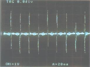
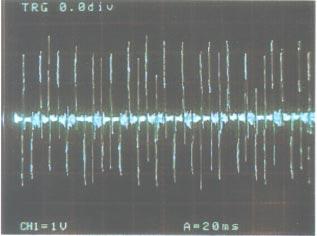
5 Impulsive Synchronization of Chaotic and Hyperchaotic Circuits 1397 Fig. 4. The sequence of synchronization impulses (the upper trace with vertical scale 1 V/div) and switching signal (the lower trace with vertical scale 2 V/div). The horizontal scale is 0.1 ms/div. Details of the sequence of synchronization impulses (the upper trace) and switching signal (the lower trace). The vertical scales for both channels are the same as those in. The horizontal scale is 0.1 µs/div.


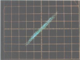
6 1398 M. Itoh et al. Fig. 5. Experimental results of the almost-identical synchronization between two Chua s oscillators with Q = s and T = s. Oscilloscope trace of v 1 versus v 1. Oscilloscope trace of v 2 versus v 2. Oscilloscope trace of i versus i. r 1 i to display the tracing on the i i plane. 1 The experimental conditions are Q = sand T= s. Observe that an almost-identical synchronization 2 is achieved. Two main factors can affect the performance of impulsive synchronization: the minimum impulse width for achieving synchronization, denoted by Q, and the frame length T. The experimental results are summarized in Fig. 6. Figure 6 shows the relation between Q and T. Observe that the relationship is almost linear except for the region when T is below s. We enlarged the region within the black box as shown in Fig. 6. To show more details, we enlarged the region within the black box in Fig. 6 as shown in Fig. 6, which is almost piecewise-linear. Figure 6(d) shows the relation between Q and the frequency of impulses F =1/T. Figure 6(e) shows the relation between Q/T and T. Observe that Q/T is approximately equal to a small constant when T is small, and a big constant when T is large. Correspondingly, we show the relation between Q/T and F in Fig. 6(f). The 1 In our experimental circuits, the resistor r is divided into two resistors r 1 =30.0Ωandr 2=38.9Ω. 2 An almost-identical synchronization is defined by the following conditions: (1) The 45-degree line on the oscilloscope screen is sufficiently thin. (2) No significant distortion is found along this 45-degree line. The experimental results can depend strongly on the measuring instruments and circuit components.
7 Fig. 6. The relationship between the minimum impulse width Q for achieving an almost-identical synchronization of two Chua s oscillators and the frame length T, or frequency of impulses F =1/T.Qversus T from 0 to s. The upper straight line Q = T is shown for comparison purpose. Q versus T from 0 to s. Q versus T (over the range of s T s). (d) Q versus frequency F. (e) Ratio Q/T versus T. (f) Ratio Q/T versus frequency F. 1399
8 (d) Fig. 6. (Continued ) 1400
9 (e) (f) Fig. 6. (Continued ) 1401
 For T 9.")
10 1402 M. Itoh et al. Fig. 7. The transmitted signal v 1 and the additive noise. Vertical scales are 2 V/div for the upper trace and 0.2 V/div for the the lower trace. Horizontal scale is 5 ms/div. following conclusions can be drawn from our experimental observations. (1) For T s To achieve an almost-identical synchronization, the impulse width occupies only 8% of the impulse period and the remaining 92% of the time period is therefore available for transmitting scrambled signals. In this case, Q increases in proportion to the length of T. Therefore, we can make Q sufficiently small with respect to T, as shown in [Yang & Chua, 1997a, 1997b; Itoh, 1999]. (2) For s T s The ratio Q/T increases from 8% to 50% as T increases. The available time interval for transmitting scrambled signals decreases. (3) For s T s To achieve an almost-identical synchronization, the impulse width occupies at least 50% of the impulse period. Therefore, Q cannot be chosen sufficiently small with respect to T. We then added noise 3 to the driving signal and examined the robustness of the impulsive synchronization to additive noise. The additive noise is shown in Fig. 7. Observe that the amplitude range of the noise is approximately 1/10 of that of v 1. In our experiments, the noise is added after the switch. The experimental results are shown in Figs with T = s. Figures 8 8 show the oscilloscope traces on the v 1 v 1 planes with Q/T = 8%, 50% and 100%, respectively. Figures 9 9 show the oscilloscope traces on the v 2 v 2 planes with Q/T = 8%, 50% and 100%, respectively. Figures show the oscilloscope traces on the i i planes with Q/T = 8%, 50% and 100%, respectively. There is no observable difference between impulsive synchronization and continuous synchronization because in Figs. 9 and 10 the thickness of the 45-degree lines for impulsive synchronization and for continuous synchronization is almost the same. Thus, the impulsive synchronization is robust to small additive noise. Furthermore, we conjecture that more accurate circuit components may be chosen to make Q much shorter Impulsive synchronization of hyperchaotic circuits The block diagram of the hyperchaotic circuit used in our experiments are shown in Fig. 11 [Matsumoto 3 FM receivers tuned at frequency 106 MHz are used to generate noise. No commercial radio station broadcasts in the frequency band around 106 MHz.


11 Fig. 8. Robustness of impulsive synchronization between Chua s oscillators to additive noise under the condition T = s. Oscilloscope traces on the v 1 v 1 planes are shown. Q/T is equal to 8%. Q/T is equal to 50%. Q/T is equal to 100%. This condition is equivalent to continuous synchronization. Fig. 9. Robustness of impulsive synchronization between Chua s oscillators to additive noise under the condition T = s. Oscilloscope traces on the v 2 v 2 planes are shown. Q/T is equal to 8%. Q/T is equal to 50%. Q/T is equal to 100%. This condition is equivalent to continuous synchronization. 1403

 i 2, (8) L 1 di 1 dt = v 1 r 1 i 1 + Ri 1, (9) Fig. 10.")


12 1404 M. Itoh et al. Fig. 11. Circuit diagram of the hyperchaotic circuit used in our experiments. et al., 1986]. The state equation of this circuit is given by C 1 dv 1 dt = g(v 2 v 1 ) i 1, (7) C 2 dv 2 dt = g(v 2 v 1 ) i 2, (8) L 1 di 1 dt = v 1 r 1 i 1 + Ri 1, (9) Fig. 10. Robustness of impulsive synchronization between Chua s oscillators to additive noise under the condition T = s. Oscilloscope traces on the i i planes are shown. Q/T is equal to 8%. Q/T is equal to 50%. Q/T is equal to 100%. This condition is equivalent to continuous synchronization. di 2 L 2 dt = v 2 r 2 i 2, (10) where g( ) isthev icharacteristic of Chua s diode, defined by g(v 2 v 1 )=G a (v 2 v 1 )+ 1 2 (G b G a ) ( v 2 v 1 B p v 2 v 1 +B p ), (11)
-plane. Projection of the chaotic attractor onto the (v 1,v 2)-plane.")
 r 1 =71.2Ω, r 2 =42.9Ω, G a =31.6mS, G b = 0.667 ms, B p =0.50 V.")
![(13) These parameters are different from the original parameters used in [Matsumoto et al., 1986] because we have some difficulties in building a circuit with the same parameters.](/docs-images/89/99045164/images/13-2.jpg "Different projections of the observed attractor for this hyperchaotic circuit are showninfig.12.")

13 Impulsive Synchronization of Chaotic and Hyperchaotic Circuits 1405 Fig. 12. Observed strange attractor from the hyperchaotic circuit used in our experiments. Projection of the chaotic attractor onto the (v 1,v 2 v 1)-plane. Projection of the chaotic attractor onto the (v 1,v 2)-plane. Projection of the chaotic attractor onto the (v 1,i 1)-plane. (d) Projection of the chaotic attractor onto the (v 2,i 2)-plane. (d) where B p is the breakpoint voltage of Chua s diode. The parameters are chosen as follows: C 1 = 102 nf, C 2 = 318 nf, L 1 =29.9mH, L 2 =22.3mH, R = 330 Ω, (12) r 1 =71.2Ω, r 2 =42.9Ω, G a =31.6mS, G b = ms, B p =0.50 V. (13) These parameters are different from the original parameters used in [Matsumoto et al., 1986] because we have some difficulties in building a circuit with the same parameters. Different projections of the observed attractor for this hyperchaotic circuit are showninfig.12. The circuit diagram of impulsive synchronization of the two hyperchaotic circuits is shown in Fig. 13. The two voltage buffers send two signals v 2 v 1 and Ri 1 to a switch controlled by two switching signals. Although samples from the two signals are sent to the driven circuit, we use a timedivision scheme to transmit both impulse sequences through only one communication channel. In this case, each frame consists of three regions. The first two regions are synchronization regions consisting of driving impulses. The first region is used

14 1406 Fig. 13. Circuit diagram of impulsive synchronization between two hyperchaotic circuits.


15 Impulsive Synchronization of Chaotic and Hyperchaotic Circuits 1407 Fig. 14. Two switching signals are used to implement our time-division scheme for sending two impulse sequences through a single channel. to transmit synchronization impulses sampled from signal v 2 v 1, and the second region is used to transmit those sampled from signal Ri 1. The third region can be used to transmit scrambled message signals. In the experiments presented in this section, we did not use the third region to transmit message signals. Figure 14 shows the two switching signals used to choose and set the timing of two kinds of synchronization impulses sampled from v 2 v 1 and Ri 1. Observe that the time shift between the high voltage levels in these two switching signals correspond to the time-division scheme for sending both impulse sequences through a single channel. Figure 15 shows two synchronization impulse sequences sampled from v 2 v 1 and Ri 1. Observe that the slight time shift between these two sequences corresponds to the two switching signals shown in Fig. 14. Figure 15 shows the impulse sequence transmitted through the single channel. Observe that these two kinds of synchronization impulses are transmitted over different time slots in each frame. Figures 16 and 16 show the tracings in the v 1 v 1 plane and v 2 v 2 plane for Q/T =0.26 and T = s, respectively. Observe that an almost-identical synchronization is achieved. The experimental results of the relations between Q and T are summarized in Fig. 17. Figure 17 shows the relation between Q and T. Observe that the relationship is almost piecewiselinear. In Fig. 17, we enlarged the almost linear region shown in the black box in Fig. 17. Figure 17 shows the relation between Q and the Fig. 15. Impulse sequences for impulsive synchronization of two hyperchaotic circuits. Two impulse sequences shown separately. The upper trace is the impulse sequence sampled from the voltage v 2 v 1 across Chua s diode. The lower trace is the impulse sequence sampled from the voltage Ri across the negative resistor. The transmitted impulse sequence through a single channel shared by the two impulse sequences shown in under our time-division scheme. impulse frequency F. Figure 17(d) shows the relation between Q/T and T. Correspondingly, we show the relation between Q/T and F in Fig. 17(e). The following conclusions can be drawn from our experimental observations. (1) For s T s The ratio Q/T falls from 47% to 26% as T increases. The available region T 2Q for transmitting scrambled signals increases gradually.


16 1408 M. Itoh et al. Fig. 16. Impulsive synchronization between two hyperchaotic circuits under the conditions Q/T =0.26 and T = s. Oscilloscope trace of v 1 versus v 1. Oscilloscope trace of v 2 versus v 2. Fig. 17. The relationship between the minimum impulse width Q for achieving an almost-identical synchronization of two hyperchaotic circuits and the frame length T, or frequency of impulses F =1/T. Q versus T from 0 to s. The upper straight line Q =1/2T is shown for comparison purpose. Q versus T (over the range of s T s). Q versus frequency F. (d) Ratio Q/T versus T. (e) Ratio Q/T versus frequency F.
17 Fig. 17. (Continued ) 1409
18 (d) (e) Fig. 17. (Continued ) 1410
 and the additive noise (lower trace).")


19 Fig. 18. Impulse sequence and additive noise. Horizontal scale is 2 ms/div. The transmitted signal (upper trace) and the additive noise (lower trace). Vertical scales are 5.0 V/div for the upper trace and 0.2 V/div for the lower trace, respectively. The signal v 2 v 1 (upper trace) and the additive noise (lower trace). Vertical scales are 0.5 V/div for the upper trace and 0.2 V/div for the lower trace, respectively. The signal v 1 (upper trace) and the additive noise (lower trace). Vertical scales are 1.0 V/div for the upper trace and 0.2 V/div for the lower trace, respectively. Fig. 19. Impulsive synchronization between two hyperchaotic circuits when the additive channel noise shown in Fig. 18 is added with T = s. Oscilloscope trace of v 1 versus v 1 with Q/T =0.26. Oscilloscope trace of v 1 versus v 1 with Q/T =0.40. Oscilloscope trace of v 1 versus v 1 with Q/T =1.0; namely, continuous synchronization. 1411
 of the frame length for transmitting synchronization impulses.")
 For 1.3 10 5 s T 2.")

20 1412 M. Itoh et al. (2) For s T s The ratio Q/T is equal to 26%. In this case, an almost-identical synchronization requires at least 52% (= 2Q/T = 26% 2) of the frame length for transmitting synchronization impulses. In this case, 48% of the frame length is available for transmitting message signals. In this case, Q increases in proportion to T. (3) For s T s The ratio Q/T rises from 26% to 50% as T increases. The available time slot for transmitting information signals decreases. (4) For s T s An almost-identical synchronization requires 100% (= 50% 2) of the frame length for transmitting synchronization impulses. No time slot is available for transmitting information signals. We then examine the robustness of the impulsive synchronization to small additive noise. Figure 18 shows the transmitted impulse sequence and the additive noise. To compare the amplitudes of impulses and noise, Fig. 18 shows the signal v 2 v 1 and the additive noise. Figure 18 shows the signal v 1 and the additive noise. The experimental results are shown in Figs. 19 and 20 with T = s. Figures show the oscilloscope traces on the v 1 v 1 planes with Q/T = 26%, 40% and 100%, respectively. Figure show the oscilloscope traces on the v 2 v 2 planes with Q/T = 26%, 40% and 100%, respectively. There is no observable difference between impulsive synchronization and continuous synchronization because in Figs. 19 and 20 the thickness of the 45-degree lines for impulsive synchronization and for continuous synchronization are almost the same. The above observations show that impulsive synchronization of the hyperchaotic circuit in Fig. 11 is robust to small additive noise. Fig. 20. Impulsive synchronization between two hyperchaotic circuits when the additive channel noise shown in Fig. 18 is added with T = s. Oscilloscope trace of v 2 versus v 2 with Q/T = Oscilloscope trace of v 2 versus v 2 with Q/T = Oscilloscope trace of v 1 versus v 1 with Q/T =1.0; namely, continuous synchronization. 3. Spread Spectrum Communication Systems In chaotic spread spectrum communication systems, there are different ways to modulate the message signal s(t) with a chaotic spreading carrier c(t). For example, one can multiply c(t) withs(t) (direct sequence modulation [Yang & Chua, 1997a,

21 1413 Fig. 21. Circuit diagrams of chaotic spread spectrum communication systems used in our experiments when additive and DS modulations are used. When the Chua s oscillators are used to generate the chaotic spreading carriers. When the hyperchaotic circuits are used to generate the chaotic spreading carriers.
")
22 1414 Fig. 21. (Continued )


 Q/T = 18% and T =8.0 10 6 s.")
23 (d) (e) Fig. 22. Message signals and recovered message signals when the systems in Fig. 21 is used with additive modulation. Message signals are shown in upper traces and the recovered message signals are shown in lower traces. Q/T = 10% and T = s. Q/T = 50% and T = s. Q/T = 80% and T = s. (d) Q/T =8%and T= s. (e) Q/T = 18% and T = s. (f) Q/T = 50% and T = s. (f) 1415
![1416 M. Itoh et al. 1998a, 1998b; Itoh, 1999]). One can also add s(t) to c(t) (chaotic masking [Kocarev et al., 1992]).](/docs-images/89/99045164/images/24-0.jpg "For relatively low security situations, we can easily implement the chaotic masking scheme by using impulsive synchronization.")
 from p(t) within the region T Q (here, c(t) isthe chaotic carrier recovered using impulsive synchronization at the receiver end).")
24 1416 M. Itoh et al. 1998a, 1998b; Itoh, 1999]). One can also add s(t) to c(t) (chaotic masking [Kocarev et al., 1992]). For relatively low security situations, we can easily implement the chaotic masking scheme by using impulsive synchronization. The synchronization region Q of each frame consists of synchronization impulses while the rest of the frame consists of the masked signal p(t) = s(t)+ c(t). The recovery of the message signal is performed by subtracting c(t) from p(t) within the region T Q (here, c(t) isthe chaotic carrier recovered using impulsive synchronization at the receiver end). Therefore, the recovering process is a little simpler than that proposed in [Kocarev et al., 1992]. Similarly, the direct sequence (DS) modulation can be easily implemented by impulsive synchronization. In the spread spectrum communication systems based on impulsive synchronization presented in this section, within each frame of T seconds, the message signal takes only T Q seconds. Since Q is not small with respect to T, the recovered signal r(t) is periodically sampled for every T seconds. Thus, for a reliable recovery the message signal s(t) should be bandlimited to a frequency range below 1/2T in accordance with the sampling theorem. The block diagram of the chaotic spread spectrum communication systems based on impulsive synchronization is shown in Fig. 21. Figure 21 shows the block diagram based on Chua s oscillators. The modulator at the transmitter end will scramble the message signal with the chaotic masks by using either addition or multiplication. The switch is between v 1 and the modulated message signal. Correspondingly, Fig. 21 shows the block diagram based on hyperchaotic circuits. The experimental results with Chua s oscillators and additive modulation are shown in Fig. 22. The message signal is a triangular waveform. Figure 22 shows the message signal and the recovered message signal under the conditions Q/T = 10% and T = s. Figure 22 shows the message signal and the recovered message signal under the conditions Q/T = 50% and T = s. Figure 22 shows the message signal and the recovered message signal under the conditions Q/T = 80% and T = s. Observe from Figs that the recovered signals have very little distortions. Figure 22(d) shows the message signal and the recovered message signal under the conditions Q/T =8%andT = s. Significant distortions in the recovered message Fig. 23. The transmitted signals with or without modulated message signals under the conditions Q/T = 10% and T = s. The chaotic systems are Chua s oscillators. Transmitted signal without the modulated message signal. Transmitted signal with the modulated message signal when additive modulation is used. signal can now be observed. Figure 22(e) shows the message signal and the recovered message signal under the conditions Q/T = 18% and T = s. Figure 22(f) shows the message signal and the recovered message signal under the conditions Q/T = 50% and T = s. Observe from Figs. 22(e) and 22(f) that the recovered signals have very little distortions. To show what the transmitted signal in the channel looks like, in Fig. 23 the mixture of the impulse sequence and the chaotic carrier c(t) is shown. Figure 23 shows the mixture of the
 and recovered message signal (the lower trace). Q/T = 26% and T =5.0 10 6 s. Message signal (the upper trace) and recovered message signal (the lower trace).")
 impulse sequence and the modulated message signal c(t)+s(t). Our experimental results on the hyperchaotic circuits with additive modulation are shown in Fig. 24.")

 shows the mixture of the impulse sequence and the modulated message signal c(t)+ s(t).")
25 Impulsive Synchronization of Chaotic and Hyperchaotic Circuits 1417 Fig. 24. Different kinds of signals observed in experiments when hyperchaotic circuits and additive modulation are used. Message signal (the upper trace) and recovered message signal (the lower trace). Q/T = 26% and T = s. Message signal (the upper trace) and recovered message signal (the lower trace). Q/T = 26% and T = s. Transmitted signal without the modulated message signal. (d) Transmitted signal with the modulated message signal. (d) impulse sequence and the modulated message signal c(t)+s(t). Our experimental results on the hyperchaotic circuits with additive modulation are shown in Fig. 24. The message signal is also a triangular waveform. Figure 24 shows the message signal and the recovered message signal under the conditions Q/T = 26% and T = s. Figure 24 shows the message signal and the recovered message signal under the conditions Q/T = 26% and T = s. Observe that there exists almost no distortions in the recovered signals. To show what the transmitted signal in the channel looks like, in Fig. 24 the mixture of the impulse sequence and the chaotic carrier c(t) is shown. Figure 24(d) shows the mixture of the impulse sequence and the modulated message signal c(t)+ s(t). In the DS modulation, the message signal is multiplied by the chaotic spreading carrier at the transmitter and the transmitted signal is divided by the recovered chaotic spreading carrier at the receiver end. In our experiments, we use AD533 IC chips as multipliers and dividers. In the AD533

 (the upper trace) and the recovered message")
 (the upper trace) and the recovered message")

26 1418 M. Itoh et al. Fig. 25. Experimental results when DS modulation and Chua s oscillators are used. v 1 is chosen as the chaotic spreading carrier. Q/T = 10% and T = s. The triangular message signal s(t) (the upper trace) and the recovered message signal r(t) (the lower trace). The binary message signal s(t) (the upper trace) and the recovered message signal r(t) (the lower trace). Transmitted signal. Fig. 26. Experimental results when DS modulation and Chua s oscillators are used. v 2 is chosen as the chaotic spreading carrier. Q/T = 10% and T = s. The triangular message signal s(t) (the upper trace) and the recovered message signal r(t) (the lower trace). The binary message signal s(t) (the upper trace) and the recovered message signal r(t) (the lower trace). Transmitted signal.

 (the upper trace) and the recovered message")
 (the upper trace) and the recovered message")

27 Fig. 27. Experimental results when DS modulation and Chua s oscillators are used. Here, v 1 is chosen as the chaotic spreading carrier. Q/T =8%andT = s. The triangular message signal s(t) (the upper trace) and the recovered message signal r(t) (the lower trace). The binary message signal s(t) (the upper trace) and the recovered message signal r(t) (the lower trace). Transmitted signal. Fig. 28. Experimental results when DS modulation and Chua s oscillators are used. Here, v 2 is chosen as the chaotic spreading carrier. Q/T =8%andT = s. The triangular message signal s(t) (the upper trace) and the recovered message signal r(t) (the lower trace). The binary message signal s(t) (the upper trace) and the recovered message signal r(t) (the lower trace). Transmitted signal. 1419
 (the upper trace) and the recovered message signal r(t) (the lower trace).")


28 1420 M. Itoh et al. Fig. 29. Experimental results when DS modulation and hyperchaotic circuits are used. Here, v 2 v 1 is chosen as the chaotic spreading carrier. Q/T = 34% and T = s. The triangular message signal s(t) (the upper trace) and the recovered message signal r(t) (the lower trace). The binary message signal s(t) (the upper trace) and the recovered message signal r(t) (the lower trace). Transmitted signal. chip, the division operations are not performed in the negative regions of the input signals, thereby giving rise to interruptions in the recovering process. Furthermore, the recovered signals are saturated in the negative regions. If AD532 chips are used instead, then the division is performed well in the negative regions and better results can be expected. The experimental results for the DS modulation when Chua s oscillators are used are shown in Figs Figure 25 shows the results when the message signal s(t) is modulated by v 1 (t); namely, the modulated message signal is v 1 (t)s(t). Conditions are given by: Q/T = 10% and T = s. Figure 25 shows the triangular message signal and the recovered message signal. Figure 25 shows the binary message signal and the recovered message signal. Observe that whenever the recovered chaotic carrier ṽ 1 (t) is in the negative region, the recovered result jumps to a saturated value. But the message signal is recovered when ṽ 1 (t) ispositive. Figure 25 shows the transmitted signal, which consists of both synchronization impulses and the modulated message signal. Figure 26 shows the results when the message signal s(t) is modulated by v 2 (t); namely, the modulated message signal is v 2 (t)s 1 (t). Conditions are given by: Q/T = 10% and T = s. Figure 26 shows the triangular message signal and the recovered message signal. Figure 26 shows the binary message signal and the recovered message signal. Since the recovered carrier ṽ 2 (t) switches between positive and negative regions at a rather high frequency, the recovered signals are modulated by short impulses. By using low-pass filters, we can easily improve the recovered message signals. Figure 26 shows the transmitted signal, which consists of both synchronization impulses and the modulated message signal. Figure 27 shows the results when the message signal s(t) is modulated by v 1 (t) under the conditions Q/T =8%andT = s. Figure 27 shows the triangular message signal and the recovered message signal. Figure 27 shows the binary message signal and the recovered message signal. Figure 27 shows the transmitted signal, which consists of both synchronization impulses and the modulated message signal. Figure 28 shows the results when the message signal s(t) is modulated by v 2 (t) under the conditions Q/T =8%andT = s. Figure 27
 of Chua s oscillator is chosen as the chaotic spreading carrier and DS modulation is used. Q/T = 10%, T =20µs.")
 Oscilloscope trace of v 2 v 2 plane. (d) shows the triangular message signal and the recovered message signal.")


29 Impulsive Synchronization of Chaotic and Hyperchaotic Circuits 1421 Fig. 30. Experimental results on robustness of spread spectrum communication systems to additive channel noise. The voltage v 1(t) of Chua s oscillator is chosen as the chaotic spreading carrier and DS modulation is used. Q/T = 10%, T =20µs. The binary message signal s(t) (the upper trace) and the recovered message signal r(t) (the lower trace). Transmitted signal (the upper trace) and additive channel noise (the lower trace). Oscilloscope trace of v 1 v 1 plane. (d) Oscilloscope trace of v 2 v 2 plane. (d) shows the triangular message signal and the recovered message signal. Figure 27 shows the binary message signal and the recovered message signal. Figure 27 shows the transmitted signal, which consists of both synchronization impulses and the modulated message signal. The experimental results for the DS modulation when hyperchaotic circuits are used are shown in Fig. 29. The message signal s(t) is modulated by (v 2 (t) v 1 (t)); namely, the modulated message signal is (v 2 (t) v 1 (t))s 1 (t). Conditions are given by: Q/T = 34% and T = s. Figure 29 shows the triangular message signal and the recovered message signal. Figure 29 shows the binary message signal and the recovered message signal. Figure 29 shows the transmitted signal, which consists of both synchronization impulses and the modulated message signal. From the above experimental results we conclude that both chaotic spread spectrum communication systems work well. We also conclude that impulsive synchronization is useful for
 of Chua s oscillator is chosen as the chaotic spreading carrier and DS modulation is used. Q/T = 10%, T =20µs.")
 Oscilloscope trace of v 2 v 2 plane. (d) synchronizing chaotic systems in the transmitter and the receiver even though Q is not small.")


30 1422 M. Itoh et al. Fig. 31. Experimental results on robustness of spread spectrum communication systems to additive channel noise. The voltage v 2(t) of Chua s oscillator is chosen as the chaotic spreading carrier and DS modulation is used. Q/T = 10%, T =20µs. The binary message signal s(t) (the upper trace) and the recovered message signal r(t) (the lower trace). Transmitted signal (the upper trace) and additive channel noise (the lower trace). Oscilloscope trace of v 1 v 1 plane. (d) Oscilloscope trace of v 2 v 2 plane. (d) synchronizing chaotic systems in the transmitter and the receiver even though Q is not small. We have also evaluated the robustness of chaotic spread spectrum communication systems based on impulsive synchronization by adding noise into the communication channel. Only cases when the message signals are binary are studied in our experiments. Figures 30 and 31 show experimental results when Chua s oscillators and DS modulations are used. Figure 30 shows the results when the chaotic spreading carrier is v 1 (t). Figure 30 shows the binary message signal and the recovered message signal. Observe that the result can be easily improved by low-pass filtering and thresholding. The channel noise is shown in Fig. 30. Observe that the amplitude of the additive channel noise is around 1/10 of that of the transmitted signal. Figures 30 and 30(d) show the oscilloscope traces on the v 1 v 1 and v 2 v 2 planes, respectively. Observe that the synchronization error is small. Figure 31 shows the results when the chaotic spreading carrier is v 2 (t). Figure 31 shows the binary message signal and the recovered message signal. This result can also be improved by
 v 1(t) of the hyperchaotic circuit is chosen as the chaotic spreading carrier and DS modulation is used. Q/T = 34%, T = 2.5 µs.")
 Oscilloscope trace of v 2 v 2 plane. (d) low-pass filtering and thresholding. The channel noise is shown in Fig. 31.")
 show the oscilloscope traces on the v 1 v 1 and v 2 v 2 planes, respectively. Observe that the synchronization error is small.")

31 Impulsive Synchronization of Chaotic and Hyperchaotic Circuits 1423 Fig. 32. Experimental results on robustness of spread spectrum communication systems to additive channel noise. The voltage v 2(t) v 1(t) of the hyperchaotic circuit is chosen as the chaotic spreading carrier and DS modulation is used. Q/T = 34%, T = 2.5 µs. The binary message signal s(t) (the upper trace) and the recovered message signal r(t) (the lower trace). Transmitted signal (the upper trace) and additive channel noise (the lower trace). Oscilloscope trace of v 1 v 1 plane. (d) Oscilloscope trace of v 2 v 2 plane. (d) low-pass filtering and thresholding. The channel noise is shown in Fig. 31. Observe that the amplitude of the additive channel noise is around 1/10 of that of the chaotic spreading carrier. Figures 31 and 31(d) show the oscilloscope traces on the v 1 v 1 and v 2 v 2 planes, respectively. Observe that the synchronization error is small. Figure 32 shows experimental results when the hyperchaotic circuits and DS modulations are used. The chaotic spreading carrier is v 2 (t) v 1 (t). Figure 32 shows the binary message signal and the recovered message signal. We can easily improve the recovered results by low-pass filtering and thresholding. The channel noise is shown in Fig. 32. In this case, the amplitude of the noise is almost 1/2 of that of the transmitted signal. Figure 32 and 32(d) show the oscilloscope traces on the v 1 v 1 and v 2 v 2 planes, respectively. Observe that the synchronization error is small. From our experiments we found that the binary message signal can be completely recovered if the SNR is around 12 db. In this case, the 45-degree lines become very thick. This means that we can recover the binary information signal even if
32 1424 M. Itoh et al. the synchronization is far from the desired almostidentical synchronization. Furthermore, if we use some error-correction coding techniques, the binary message signal can be completely recovered even under a low SNR. 4. Concluding Remarks We have presented a series of experimental results on the impulsive synchronizations between two Chua s oscillators and two hyperchaotic circuits. Our experimental results show that the impulsive synchronization is very robust to both parameter mismatch and channel noise. We have also found that the performance of impulsive synchronization depends heavily on the frequency and the width of the synchronization impulses. We have presented our experimental results on chaotic spread spectrum communication systems based on impulsive synchronizations. Our experimental results show that both additive modulation and DS modulation are robust enough to channel noise. Our experimental results also suggest that impulsive synchronization is a promising approach in the design of practical chaotic spread spectrum communication systems. Acknowledgment This work is supported in part by the Office of Naval Research(ONR) under grant numbers N and N References Chua, L. O., Kocarev, L., Eckert, K. & Itoh, M. [1992] Experimental chaos synchronization in Chua s circuit, Int. J. Bifurcation and Chaos 2(3), Chua, L. O., Itoh, M., Kocarev, L. & Eckert, K. [1993] Chaos synchronization in Chua s circuit, J. Circuits Syst. Comput. 3(1), Dedieu, H., Kennedy, M. & Hasler, M. [1993] Chaos shift keying: Modulation and demodulation of a chaotic carrier using self-synchronizing Chua s circuits, IEEE Trans. Circuits Syst. CAS-40(10), Halle, K. S., Wu C. W., Itoh, M. & Chua, L. O. [1992] Spread spectrum communication through modulation of chaos, Int. J. Bifurcation and Chaos 3(2), Itoh, M. & Murakami, H. [1995] New communication systems via chaotic synchronizations and modulations, IEICE Trans. Fundamentals E78-A(3), Itoh, M. [1999] Spread spectrum communication via chaos, Int. J. Bifurcation and Chaos 9(1), Kocarev,L.,Halle,K.S.,Eckert,K.,Chua,L.O.& Parlitz, U. [1992] Experimental demonstration of secure communications via chaotic synchronization, Int. J. Bifurcation and Chaos 2(3), Lipton, J. M. & Dabke, K. P. [1996] Spread spectrum communications based on chaotic systems, Int. J. Bifurcation and Chaos 6(12A), Madan, R. [1993] Chua s Circuit: A Paradigm for Chaos (World Scientific, Singapore). Matsumoto, T., Chua, L. O. & Kobayashi, K. [1986] Hyperchaos: Laboratory experiment and numerical confirmation, IEEE Trans. Circuits Syst. CAS-33(11), Panas, A. I., Yang, T. & Chua, L. O. [1998] Experimental results of impulsive synchronization between two Chua s circuits, Int. J. Bifurcation and Chaos 8(3), Parlitz,U.,Chua,L.O.,Kocarev,L.,Halle,S.&Shang, A. [1992] Transmission of digital signals by chaotic synchronization, Int. J. Bifurcation and Chaos 2(4), Parlitz, U. & Ergezinger, S. [1994] Robust communication based on chaotic spreading sequences, Phys. Lett. A188, Pecora, L. & Carroll, T. [1990] Synchronization in chaotic systems, Phys. Rev. Lett. 64(8), Yang, T. & Chua, L. O. [1997a] Impulsive control and synchronization of nonlinear dynamical systems and application to secure communication, Int. J. Bifurcation and Chaos 7(3), Yang, T. & Chua, L. O. [1997b] Chaotic digital code-division multiple access (CDMA) communication systems, Int. J. Bifurcation and Chaos 7(12), Yang, T. & Chua, L. O. [1997c] Impulsive stabilization for control and synchronization of chaotic systems: Theory and application to secure communication, Trans. Circuits Syst. I 44(10), Yang, T. & Chua, L. O. [1998a] Applications of chaotic digital code-division multiple access (CDMA) to cable communication systems, Int. J. Bifurcation and Chaos 8(8), Yang, T. & Chua, L. O. [1998b] Error performance of chaotic digital code-division multiple access (CDMA) systems, Int. J. Bifurcation and Chaos 8(10),
Communicating using filtered synchronized chaotic signals. T. L. Carroll
 Communicating using filtered synchronized chaotic signals. T. L. Carroll Abstract- The principles of synchronization of chaotic systems are extended to the case where the drive signal is filtered. A feedback
A Synthetic Inductor Implementation of Chua's Circuit
 A Synthetic Inductor Implementation of Chua's Circuit Bharathwaj Muthuswamy Tamara Blain Kyle Sundqvist Electrical Engineering and Computer Sciences University of California at Berkeley Technical Report
Rich Variety of Bifurcation and Chaos in a Simple Non-Source Free Electronic Circuit with a Diode
 International Journal of Pure and Applied Physics ISSN 0973-1776 Volume 6, Number 1 (2010), pp. 63 69 Research India Publications http://www.ripublication.com/ijpap.htm Rich Variety of Bifurcation and
IN THIS PAPER, we present a new, general design 1 for
 IEEE TRANSACTIONS ON CIRCUITS AND SYSTEMS I: FUNDAMENTAL THEORY AND APPLICATIONS, VOL. 44, NO. 5, MAY 1997 373 A New Approach to Communications Using Chaotic Signals Ned J. Corron, Member, IEEE, and Daniel
A SURVEY OF CHAOTIC SECURE COMMUNICATION SYSTEMS
 International Journal of Computational Cognition (http://www.yangsky.com/yangijcc.htm) Volume 2, Number 2, Pages 81 13, June 24 Publisher Item Identifier S 1542-598(4)125-4/$2. Article electronically published
REVIEW OF CIRCUIT IMPLEMENTATION OF SYNCHRONIZED CHAOS WITH APPLICATION TO COMMUNICATION BY: ABHISHEK SINGH AND DIVYA GROVER
 REVIEW OF CIRCUIT IMPLEMENTATION OF SYNCHRONIZED CHAOS WITH APPLICATION TO COMMUNICATION BY: ABHISHEK SINGH AND DIVYA GROVER INTRODUCTION: In this Project, we focus on the synchronizing properties of the
LORENZ-BASED CHAOTIC SECURE COMMUNICATION SCHEMES
 LORENZ-BASED CHAOTIC SECURE COMMUNICATION SCHEMES I.A. Kamil and O.A. Fakolujo Department of Electrical and Electronic Engineering University of Ibadan, Nigeria ismaila.kamil@ui.edu.ng ABSTRACT Secure
Performance Analysis of Correlation-Based Communication Schemes Utilizing Chaos
 1684 IEEE TRANSACTIONS ON CIRCUITS AND SYSTEMS I: FUNDAMENTAL THEORY AND APPLICATIONS, VOL. 47, NO. 12, DECEMBER 2000 Performance Analysis of Correlation-Based Communication Schemes Utilizing Chaos Mikhail
A New Chaotic Secure Communication System
 1306 IEEE TRANSACTIONS ON COMMUNICATIONS, VOL 51, NO 8, AUGUST 2003 A New Chaotic Secure Communication System Zhengguo Li, Kun Li, Changyun Wen, and Yeng Chai Soh Abstract This paper proposes a digital
Chaotic-Based Processor for Communication and Multimedia Applications Fei Li
 Chaotic-Based Processor for Communication and Multimedia Applications Fei Li 09212020027@fudan.edu.cn Chaos is a phenomenon that attracted much attention in the past ten years. In this paper, we analyze
TDMA SECURE COMMUNICATION SCHEME BASED ON SYNCHRONIZATION OF CHUA S CIRCUITS
 Journal of Circuits, Systems, and Computers, Vol 1, Nos 3 & 4 (2) 147 158 c World Scientific Publishing Company TDMA SECURE COMMUNICATION SCHEME BASED ON SYNCHRONIZATION OF CHUA S CIRCUITS ZHENYA HE, KE
Communicating with noise: How chaos and noise combine to generate secure encryption keys
 CHAOS VOLUME 8, NUMBER 3 SEPTEMBER 1998 Communicating with noise: How chaos and noise combine to generate secure encryption keys Ali A. Minai a) and T. Durai Pandian Complex Adaptive Systems Laboratory,
Communication using Synchronization of Chaos in Semiconductor Lasers with optoelectronic feedback
 Communication using Synchronization of Chaos in Semiconductor Lasers with optoelectronic feedback S. Tang, L. Illing, J. M. Liu, H. D. I. barbanel and M. B. Kennel Department of Electrical Engineering,
A NOVEL FREQUENCY-MODULATED DIFFERENTIAL CHAOS SHIFT KEYING MODULATION SCHEME BASED ON PHASE SEPARATION
 Journal of Applied Analysis and Computation Volume 5, Number 2, May 2015, 189 196 Website:http://jaac-online.com/ doi:10.11948/2015017 A NOVEL FREQUENCY-MODULATED DIFFERENTIAL CHAOS SHIFT KEYING MODULATION
BEING wideband, chaotic signals are well suited for
 680 IEEE TRANSACTIONS ON CIRCUITS AND SYSTEMS II: EXPRESS BRIEFS, VOL. 51, NO. 12, DECEMBER 2004 Performance of Differential Chaos-Shift-Keying Digital Communication Systems Over a Multipath Fading Channel
Project: IEEE P Working Group for Wireless Personal Area Networks N
 Project: IEEE P80.15 Working Group for Wireless Personal Area Networks N (WPANs( WPANs) Title: [UWB Direct Chaotic Communications Technology] Date Submitted: [15 November, 004] Source: [(1) Y. Kim, C.
IEEE TRANSACTIONS ON CIRCUITS AND SYSTEMS I: REGULAR PAPERS, VOL. 51, NO. 2, FEBRUARY
 IEEE TRANSACTIONS ON CIRCUITS AND SYSTEMS I: REGULAR PAPERS, VOL 51, NO 2, FEBRUARY 2004 391 Coexistence of Chaos-Based and Conventional Digital Communication Systems of Equal Bit Rate Francis C M Lau,
A New Secure Communication Model Based on Synchronization of Coupled Multidelay Feedback Systems
 A New Secure Communication Model Based on Synchronization of Coupled Multidelay Feedback Systems Thang Manh Hoang Abstract Recent research result has shown that two multidelay feedback systems can synchronize
TRANSMITING JPEG IMAGE OVER USING UPA AND CHOTIC COMMUNICATION
 TRANSMITING JPEG IMAGE OVER MIMO USING UPA AND CHOTIC COMMUNICATION Pravin B. Mali 1, Neetesh Gupta 2,Amit Sinhal 3 1 2 3 Information Technology 1 TIT, Bhopal 2 TIT, Bhopal 3 TIT, Bhopal 1 pravinmali598@gmail.com
Kolumbán, Géza; Kennedy, Michael Peter
 Title Author(s) The role of synchronization in digital communications using chaos - part III: performance bounds for correlation receivers Kolumbán, Géza; Kennedy, Michael Peter Publication date 2000-12
Part A: Spread Spectrum Systems
 1 Telecommunication Systems and Applications (TL - 424) Part A: Spread Spectrum Systems Dr. ir. Muhammad Nasir KHAN Department of Electrical Engineering Swedish College of Engineering and Technology February
Complex Dynamic Phenomena in Power Converters: Bifurcation Analysis and Chaotic Behavior
 Complex Dynamic Phenomena in Power Converters: Bifurcation Analysis and Chaotic Behavior DONATO CAFAGNA, GIUSEPPE GRASSI Dipartimento Ingegneria Innovazione Università di Lecce via Monteroni, 700 Lecce
DIGITAL COMMUNICATIONS (INTRODUCTION TO MULTISIM SOFTWARE)
") PROJECT 1B DIGITAL COMMUNICATIONS (INTRODUCTION TO MULTISIM SOFTWARE) (i) FSK SYSTEM (MODULATOR / DEMODULATOR) Abstract: In this project, students are required to design a complete circuit of FSK SYSTEM.
PROJECT 1B DIGITAL COMMUNICATIONS (INTRODUCTION TO MULTISIM SOFTWARE) (i) FSK SYSTEM (MODULATOR / DEMODULATOR) Abstract: In this project, students are required to design a complete circuit of FSK SYSTEM.
SYNCHRONIZATION METHODS FOR COMMUNICATION WITH CHAOS OVER BAND-LIMITED CHANNELS
 INTERNATIONAL JOURNAL OF CIRCUIT THEORY AND APPLICATIONS Int. J. Circ. ¹heor. Appl., 27: 555}567 (1999) SYNCHRONIZATION METHODS FOR COMMUNICATION WITH CHAOS OVER BAND-LIMITED CHANNELS NIKOLAI F. RULKOV*
Secure communication by chaotic synchronization: Robustness under noisy conditions
 Nonlinear Analysis: eal World Applications 8 (2007) 1003 1012 www.elsevier.com/locate/na Secure communication by chaotic synchronization: obustness under noisy conditions Amalia N. Miliou a,, Ioannis P.
Chaotic Circuits and Encryption
 Chaotic Circuits and Encryption Brad Aimone Stephen Larson June 16, 2006 Neurophysics Lab Introduction Chaotic dynamics are a behavior exhibited by some nonlinear dynamical systems. Despite an appearance
Part A: Spread Spectrum Systems
 1 Telecommunication Systems and Applications (TL - 424) Part A: Spread Spectrum Systems Dr. ir. Muhammad Nasir KHAN Department of Electrical Engineering Swedish College of Engineering and Technology March
HY448 Sample Problems
 HY448 Sample Problems 10 November 2014 These sample problems include the material in the lectures and the guided lab exercises. 1 Part 1 1.1 Combining logarithmic quantities A carrier signal with power
Amplitude Frequency Phase
 Chapter 4 (part 2) Digital Modulation Techniques Chapter 4 (part 2) Overview Digital Modulation techniques (part 2) Bandpass data transmission Amplitude Shift Keying (ASK) Phase Shift Keying (PSK) Frequency
A Multiple-Access Technique for Differential Chaos-Shift Keying
 96 IEEE TRASACTIOS O CIRCUITS AD SYSTEMS I: FUDAMETAL THEORY AD APPLICATIOS, VOL. 49, O. 1, JAUARY 2002 synchronization scheme used. For simulation purposes, take d(t) = 0:05. As seen in Fig. 4, the decryption
Data Conversion Circuits & Modulation Techniques. Subhasish Chandra Assistant Professor Department of Physics Institute of Forensic Science, Nagpur
 Data Conversion Circuits & Modulation Techniques Subhasish Chandra Assistant Professor Department of Physics Institute of Forensic Science, Nagpur Data Conversion Circuits 2 Digital systems are being used
Spread Spectrum. Chapter 18. FHSS Frequency Hopping Spread Spectrum DSSS Direct Sequence Spread Spectrum DSSS using CDMA Code Division Multiple Access
 Spread Spectrum Chapter 18 FHSS Frequency Hopping Spread Spectrum DSSS Direct Sequence Spread Spectrum DSSS using CDMA Code Division Multiple Access Single Carrier The traditional way Transmitted signal
Electric Circuit Fall 2016 Pingqiang Zhou LABORATORY 7. RC Oscillator. Guide. The Waveform Generator Lab Guide
 LABORATORY 7 RC Oscillator Guide 1. Objective The Waveform Generator Lab Guide In this lab you will first learn to analyze negative resistance converter, and then on the basis of it, you will learn to
Chaos and Analog Signal Encryption
 Course: PHY42 Instructor: Dr. Ken Kiers Date: 0/2/202 Chaos and Analog Signal Encryption Talbot Knighton Abstract This paper looks at a method for using chaotic circuits to encrypt analog signals. Two
University of Bristol - Explore Bristol Research. Peer reviewed version. Link to published version (if available): /TCSI.2001.
: /TCSI.2001.") Williams, C. (2001). Chaotic communications over radio channels. IEEE Transactions on Circuits & Systems, 48(12), 1394-1404. DOI: 10.1109/TCSI.2001.972846 Peer reviewed version Link to published version
Williams, C. (2001). Chaotic communications over radio channels. IEEE Transactions on Circuits & Systems, 48(12), 1394-1404. DOI: 10.1109/TCSI.2001.972846 Peer reviewed version Link to published version
CME312- LAB Manual DSB-SC Modulation and Demodulation Experiment 6. Experiment 6. Experiment. DSB-SC Modulation and Demodulation
 Experiment 6 Experiment DSB-SC Modulation and Demodulation Objectives : By the end of this experiment, the student should be able to: 1. Demonstrate the modulation and demodulation process of DSB-SC. 2.
Performance of Wideband Mobile Channel with Perfect Synchronism BPSK vs QPSK DS-CDMA
 Performance of Wideband Mobile Channel with Perfect Synchronism BPSK vs QPSK DS-CDMA By Hamed D. AlSharari College of Engineering, Aljouf University, Sakaka, Aljouf 2014, Kingdom of Saudi Arabia, hamed_100@hotmail.com
Chapter 4. Part 2(a) Digital Modulation Techniques
 Digital Modulation Techniques") Chapter 4 Part 2(a) Digital Modulation Techniques Overview Digital Modulation techniques Bandpass data transmission Amplitude Shift Keying (ASK) Phase Shift Keying (PSK) Frequency Shift Keying (FSK) Quadrature
Chapter 4 Part 2(a) Digital Modulation Techniques Overview Digital Modulation techniques Bandpass data transmission Amplitude Shift Keying (ASK) Phase Shift Keying (PSK) Frequency Shift Keying (FSK) Quadrature
Unit 1 Introduction to Spread- Spectrum Systems. Department of Communication Engineering, NCTU 1
 Unit 1 Introduction to Spread- Spectrum Systems Department of Communication Engineering, NCTU 1 What does it mean by spread spectrum communications Spread the energy of an information bit over a bandwidth
Laboratory Assignment 5 Amplitude Modulation
 Laboratory Assignment 5 Amplitude Modulation PURPOSE In this assignment, you will explore the use of digital computers for the analysis, design, synthesis, and simulation of an amplitude modulation (AM)
Simultaneous amplitude and frequency noise analysis in Chua s circuit
 Typeset using jjap.cls Simultaneous amplitude and frequency noise analysis in Chua s circuit J.-M. Friedt 1, D. Gillet 2, M. Planat 2 1 : IMEC, MCP/BIO, Kapeldreef 75, 3001 Leuven, Belgium
Journal of American Science 2015;11(7)
") Design of Efficient Noise Reduction Scheme for Secure Speech Masked by Signals Hikmat N. Abdullah 1, Saad S. Hreshee 2, Ameer K. Jawad 3 1. College of Information Engineering, AL-Nahrain University, Baghdad-Iraq
Design of Efficient Noise Reduction Scheme for Secure Speech Masked by Signals Hikmat N. Abdullah 1, Saad S. Hreshee 2, Ameer K. Jawad 3 1. College of Information Engineering, AL-Nahrain University, Baghdad-Iraq
Experiment No. 3 Pre-Lab Phase Locked Loops and Frequency Modulation
 Experiment No. 3 Pre-Lab Phase Locked Loops and Frequency Modulation The Pre-Labs are informational and although they follow the procedures in the experiment, they are to be completed outside of the laboratory.
Chaos based Communication System Using Reed Solomon (RS) Coding for AWGN & Rayleigh Fading Channels
 Coding for AWGN & Rayleigh Fading Channels") 2015 IJSRSET Volume 1 Issue 1 Print ISSN : 2395-1990 Online ISSN : 2394-4099 Themed Section: Engineering and Technology Chaos based Communication System Using Reed Solomon (RS) Coding for AWGN & Rayleigh
2015 IJSRSET Volume 1 Issue 1 Print ISSN : 2395-1990 Online ISSN : 2394-4099 Themed Section: Engineering and Technology Chaos based Communication System Using Reed Solomon (RS) Coding for AWGN & Rayleigh
SOME PHYSICAL LAYER ISSUES. Lecture Notes 2A
 SOME PHYSICAL LAYER ISSUES Lecture Notes 2A Delays in networks Propagation time or propagation delay, t prop Time required for a signal or waveform to propagate (or move) from one point to another point.
two computers. 2- Providing a channel between them for transmitting and receiving the signals through it.
 1. Introduction: Communication is the process of transmitting the messages that carrying information, where the two computers can be communicated with each other if the two conditions are available: 1-
Electronics Interview Questions
 Electronics Interview Questions 1. What is Electronic? The study and use of electrical devices that operate by controlling the flow of electrons or other electrically charged particles. 2. What is communication?
A new high frequency realization of Chua s chaotic circuit using current feedback operational amplifiers (CFOA s)
") International Journal of Electronics and Computer Science Engineering 223 Available Online at www.ijecse.org ISSN: 2277-1956 A new high frequency realization of Chua s chaotic circuit using current feedback
International Journal of Electronics and Computer Science Engineering 223 Available Online at www.ijecse.org ISSN: 2277-1956 A new high frequency realization of Chua s chaotic circuit using current feedback
Lecture 9: Spread Spectrum Modulation Techniques
 Lecture 9: Spread Spectrum Modulation Techniques Spread spectrum (SS) modulation techniques employ a transmission bandwidth which is several orders of magnitude greater than the minimum required bandwidth
Communication Systems Lab
 LAB MANUAL Communication Systems Lab (EE-226-F) Prepared by: Varun Sharma (Lab In-charge) Dayal C. Sati (Faculty In-charge) B R C M CET BAHAL DEPARTMENT OF ELECTRONICS & COMMUNICATION ENGINEERING Page
Digital Chaotic Synchronized Communication System
 Journal of Engineering Science and Technology Review 2 (1) (2009) 82-86 Research Article JOURNAL OF Engineering Science and Technology Review www.jestr.org Digital Chaotic Synchronized Communication System
332:223 Principles of Electrical Engineering I Laboratory Experiment #2 Title: Function Generators and Oscilloscopes Suggested Equipment:
 RUTGERS UNIVERSITY The State University of New Jersey School of Engineering Department Of Electrical and Computer Engineering 332:223 Principles of Electrical Engineering I Laboratory Experiment #2 Title:
UNIT-2 Angle Modulation System
 UNIT-2 Angle Modulation System Introduction There are three parameters of a carrier that may carry information: Amplitude Frequency Phase Frequency Modulation Power in an FM signal does not vary with modulation
EE-4022 Experiment 2 Amplitude Modulation (AM)
") EE-4022 MILWAUKEE SCHOOL OF ENGINEERING 2015 Page 2-1 Student objectives: EE-4022 Experiment 2 Amplitude Modulation (AM) In this experiment the student will use laboratory modules to implement operations
EE-4022 MILWAUKEE SCHOOL OF ENGINEERING 2015 Page 2-1 Student objectives: EE-4022 Experiment 2 Amplitude Modulation (AM) In this experiment the student will use laboratory modules to implement operations
Chapter 6 Bandwidth Utilization: Multiplexing and Spreading 6.1
 Chapter 6 Bandwidth Utilization: Multiplexing and Spreading 6.1 Copyright The McGraw-Hill Companies, Inc. Permission required for reproduction or display. 3-6 PERFORMANCE One important issue in networking
Twelve voice signals, each band-limited to 3 khz, are frequency -multiplexed using 1 khz guard bands between channels and between the main carrier
 Twelve voice signals, each band-limited to 3 khz, are frequency -multiplexed using 1 khz guard bands between channels and between the main carrier and the first channel. The modulation of the main carrier
Digital Communication System
 Digital Communication System Purpose: communicate information at required rate between geographically separated locations reliably (quality) Important point: rate, quality spectral bandwidth, power requirements
Time division multiplexing The block diagram for TDM is illustrated as shown in the figure
 CHAPTER 2 Syllabus: 1) Pulse amplitude modulation 2) TDM 3) Wave form coding techniques 4) PCM 5) Quantization noise and SNR 6) Robust quantization Pulse amplitude modulation In pulse amplitude modulation,
Problems from the 3 rd edition
 (2.1-1) Find the energies of the signals: a) sin t, 0 t π b) sin t, 0 t π c) 2 sin t, 0 t π d) sin (t-2π), 2π t 4π Problems from the 3 rd edition Comment on the effect on energy of sign change, time shifting
IFH SS CDMA Implantation. 6.0 Introduction
 6.0 Introduction Wireless personal communication systems enable geographically dispersed users to exchange information using a portable terminal, such as a handheld transceiver. Often, the system engineer
EXPERIMENT 4 - Part I: DSB Amplitude Modulation
 OBJECTIVE To generate DSB amplitude modulated signal. EXPERIMENT 4 - Part I: DSB Amplitude Modulation PRELIMINARY DISCUSSION In an amplitude modulation (AM) communications system, the message signal is
Chaotic Communications With Correlator Receivers: Theory and Performance Limits
 Chaotic Communications With Correlator Receivers: Theory and Performance Limits GÉZA KOLUMBÁN, SENIOR MEMBER, IEEE, MICHAEL PETER KENNEDY, FELLOW, IEEE, ZOLTÁN JÁKÓ, AND GÁBOR KIS Invited Paper This paper
ELEC3242 Communications Engineering Laboratory Amplitude Modulation (AM)
") ELEC3242 Communications Engineering Laboratory 1 ---- Amplitude Modulation (AM) 1. Objectives 1.1 Through this the laboratory experiment, you will investigate demodulation of an amplitude modulated (AM)
ELEC3242 Communications Engineering Laboratory 1 ---- Amplitude Modulation (AM) 1. Objectives 1.1 Through this the laboratory experiment, you will investigate demodulation of an amplitude modulated (AM)
CHAPTER 2. Instructor: Mr. Abhijit Parmar Course: Mobile Computing and Wireless Communication ( )
") CHAPTER 2 Instructor: Mr. Abhijit Parmar Course: Mobile Computing and Wireless Communication (2170710) Syllabus Chapter-2.4 Spread Spectrum Spread Spectrum SS was developed initially for military and intelligence
CHAPTER 2 Instructor: Mr. Abhijit Parmar Course: Mobile Computing and Wireless Communication (2170710) Syllabus Chapter-2.4 Spread Spectrum Spread Spectrum SS was developed initially for military and intelligence
B.Tech II Year II Semester (R13) Supplementary Examinations May/June 2017 ANALOG COMMUNICATION SYSTEMS (Electronics and Communication Engineering)
 Supplementary Examinations May/June 2017 ANALOG COMMUNICATION SYSTEMS (Electronics and Communication Engineering)") Code: 13A04404 R13 B.Tech II Year II Semester (R13) Supplementary Examinations May/June 2017 ANALOG COMMUNICATION SYSTEMS (Electronics and Communication Engineering) Time: 3 hours Max. Marks: 70 PART A
Code: 13A04404 R13 B.Tech II Year II Semester (R13) Supplementary Examinations May/June 2017 ANALOG COMMUNICATION SYSTEMS (Electronics and Communication Engineering) Time: 3 hours Max. Marks: 70 PART A
Communication Channels
 Communication Channels wires (PCB trace or conductor on IC) optical fiber (attenuation 4dB/km) broadcast TV (50 kw transmit) voice telephone line (under -9 dbm or 110 µw) walkie-talkie: 500 mw, 467 MHz
Chaos-Based Encryption of ECG Signals: Experimental Results
 J. Biomedical Science and Engineering, 2014, 7, 368-379 Published Online May 2014 in SciRes. http://www.scirp.org/journal/jbise http://dx.doi.org/10.4236/jbise.2014.76039 Chaos-Based Encryption of ECG
Nonlinear Damping of the LC Circuit using Anti-parallel Diodes. Department of Physics and Astronomy, University of North Carolina at Greensboro,
 Nonlinear Damping of the LC Circuit using Anti-parallel Diodes Edward H. Hellen a) and Matthew J. Lanctot b) Department of Physics and Astronomy, University of North Carolina at Greensboro, Greensboro,
CMOS cryptosystem using a Lorenz chaotic oscillator
 CMOS cryptosystem using a Lorenz chaotic oscillator Gonzalez, O.A.; Han, G.; Pineda de Gyvez, J.; Edgar, [No Value] Published in: Proceedings of the 1999 IEEE International Symposium on Circuits and Systems,
Energy Transfer and Message Filtering in Chaos Communications Using Injection locked Laser Diodes
 181 Energy Transfer and Message Filtering in Chaos Communications Using Injection locked Laser Diodes Atsushi Murakami* and K. Alan Shore School of Informatics, University of Wales, Bangor, Dean Street,
EXPERIMENT 3 - Part I: DSB-SC Amplitude Modulation
 OBJECTIVE To generate DSB-SC amplitude modulated signal. EXPERIMENT 3 - Part I: DSB-SC Amplitude Modulation PRELIMINARY DISCUSSION In the modulation process, the message signal (the baseband voice, video,
Fundamentals of Digital Communication
 Fundamentals of Digital Communication Network Infrastructures A.A. 2017/18 Digital communication system Analog Digital Input Signal Analog/ Digital Low Pass Filter Sampler Quantizer Source Encoder Channel
Timing Noise Measurement of High-Repetition-Rate Optical Pulses
 564 Timing Noise Measurement of High-Repetition-Rate Optical Pulses Hidemi Tsuchida National Institute of Advanced Industrial Science and Technology 1-1-1 Umezono, Tsukuba, 305-8568 JAPAN Tel: 81-29-861-5342;
PULSE CODE MODULATION TELEMETRY Properties of Various Binary Modulation Types
 PULSE CODE MODULATION TELEMETRY Properties of Various Binary Modulation Types Eugene L. Law Telemetry Engineer Code 1171 Pacific Missile Test Center Point Mugu, CA 93042 ABSTRACT This paper discusses the
A chaotic lock-in amplifier
 A chaotic lock-in amplifier Brian K. Spears Lawrence Livermore National Laboratory, 7000 East Avenue, Livermore CA 94550 Nicholas B. Tufillaro Measurement Research Lab, Agilent Laboratories, Agilent Technologies,
Multiple Access. Difference between Multiplexing and Multiple Access
 Multiple Access (MA) Satellite transponders are wide bandwidth devices with bandwidths standard bandwidth of around 35 MHz to 7 MHz. A satellite transponder is rarely used fully by a single user (for example
EXPERIMENT 2: Frequency Shift Keying (FSK)
") EXPERIMENT 2: Frequency Shift Keying (FSK) 1) OBJECTIVE Generation and demodulation of a frequency shift keyed (FSK) signal 2) PRELIMINARY DISCUSSION In FSK, the frequency of a carrier signal is modified
EXPERIMENT 2: Frequency Shift Keying (FSK) 1) OBJECTIVE Generation and demodulation of a frequency shift keyed (FSK) signal 2) PRELIMINARY DISCUSSION In FSK, the frequency of a carrier signal is modified
Exploring QAM using LabView Simulation *
 OpenStax-CNX module: m14499 1 Exploring QAM using LabView Simulation * Robert Kubichek This work is produced by OpenStax-CNX and licensed under the Creative Commons Attribution License 2.0 1 Exploring
Chapter 2 Direct-Sequence Systems
 Chapter 2 Direct-Sequence Systems A spread-spectrum signal is one with an extra modulation that expands the signal bandwidth greatly beyond what is required by the underlying coded-data modulation. Spread-spectrum
17 - Binary phase shift keying
 Name: Class: 17 - Binary phase shift keying Experiment 17 Binary Phase Shift Keying Preliminary discussion Experiments 15 and 16 show that the AM and FM modulation schemes can be used to transmit digital
CHAPTER 3 ACTIVE INDUCTANCE SIMULATION
 CHAPTER 3 ACTIVE INDUCTANCE SIMULATION The content and results of the following papers have been reported in this chapter. 1. Rajeshwari Pandey, Neeta Pandey Sajal K. Paul A. Singh B. Sriram, and K. Trivedi
ELEC Deterministic Chaos in Circuitry
 ELEC 1908 - Deterministic Chaos in Circuitry Due Midnight April 2, 2018 to Colin March 19, 2018 1 Chaos Theory Chaos is one of those words that has one meaning in common usage and another, much more precise
DEPARTMENT OF ELECTRICAL ENGINEERING AND COMPUTER SCIENCE MASSACHUSETTS INSTITUTE OF TECHNOLOGY CAMBRIDGE, MASSACHUSETTS 02139
 DEPARTMENT OF ELECTRICAL ENGINEERING AND COMPUTER SCIENCE MASSACHUSETTS INSTITUTE OF TECHNOLOGY CAMBRIDGE, MASSACHUSETTS 019.101 Introductory Analog Electronics Laboratory Laboratory No. READING ASSIGNMENT
2. TELECOMMUNICATIONS BASICS
 2. TELECOMMUNICATIONS BASICS The purpose of any telecommunications system is to transfer information from the sender to the receiver by a means of a communication channel. The information is carried by
Experiment 2: Transients and Oscillations in RLC Circuits
 Experiment 2: Transients and Oscillations in RLC Circuits Will Chemelewski Partner: Brian Enders TA: Nielsen See laboratory book #1 pages 5-7, data taken September 1, 2009 September 7, 2009 Abstract Transient
Laboratory 5: Spread Spectrum Communications
 Laboratory 5: Spread Spectrum Communications Cory J. Prust, Ph.D. Electrical Engineering and Computer Science Department Milwaukee School of Engineering Last Update: 19 September 2018 Contents 0 Laboratory
PLL FM Demodulator Performance Under Gaussian Modulation
 PLL FM Demodulator Performance Under Gaussian Modulation Pavel Hasan * Lehrstuhl für Nachrichtentechnik, Universität Erlangen-Nürnberg Cauerstr. 7, D-91058 Erlangen, Germany E-mail: hasan@nt.e-technik.uni-erlangen.de
Amplitude Modulated Systems
 Amplitude Modulated Systems Communication is process of establishing connection between two points for information exchange. Channel refers to medium through which message travels e.g. wires, links, or
Contents. Telecom Service Chae Y. Lee. Data Signal Transmission Transmission Impairments Channel Capacity
 Data Transmission Contents Data Signal Transmission Transmission Impairments Channel Capacity 2 Data/Signal/Transmission Data: entities that convey meaning or information Signal: electric or electromagnetic
Integrators, differentiators, and simple filters
 BEE 233 Laboratory-4 Integrators, differentiators, and simple filters 1. Objectives Analyze and measure characteristics of circuits built with opamps. Design and test circuits with opamps. Plot gain vs.
Digital Image Watermarking by Spread Spectrum method
 Digital Image Watermarking by Spread Spectrum method Andreja Samčovi ović Faculty of Transport and Traffic Engineering University of Belgrade, Serbia Belgrade, november 2014. I Spread Spectrum Techniques
Signal Characteristics
 Data Transmission The successful transmission of data depends upon two factors:» The quality of the transmission signal» The characteristics of the transmission medium Some type of transmission medium
ELEC3242 Communications Engineering Laboratory Frequency Shift Keying (FSK)
") ELEC3242 Communications Engineering Laboratory 1 ---- Frequency Shift Keying (FSK) 1) Frequency Shift Keying Objectives To appreciate the principle of frequency shift keying and its relationship to analogue
ELEC3242 Communications Engineering Laboratory 1 ---- Frequency Shift Keying (FSK) 1) Frequency Shift Keying Objectives To appreciate the principle of frequency shift keying and its relationship to analogue
A Novel Spread Spectrum System using MC-DCSK
 A Novel Spread Spectrum System using MC-DCSK Remya R.V. P.G. scholar Dept. of ECE Travancore Engineering College Kollam, Kerala,India Abstract A new spread spectrum technique using Multi- Carrier Differential
MAS 160/510 Additional Notes: Modulation
 MAS 160/510 Additional Notes: Modulation From Amplitude Modulation to Frequency Modulation As usually implemented, FM uses much more bandwidth than AM. You ll note, for instance, that FM radio stations
Code No: R Set No. 1
 Code No: R05220405 Set No. 1 II B.Tech II Semester Regular Examinations, Apr/May 2007 ANALOG COMMUNICATIONS ( Common to Electronics & Communication Engineering and Electronics & Telematics) Time: 3 hours
Costas Loop. Modules: Sequence Generator, Digital Utilities, VCO, Quadrature Utilities (2), Phase Shifter, Tuneable LPF (2), Multiplier
, Phase Shifter, Tuneable LPF (2), Multiplier") Costas Loop Modules: Sequence Generator, Digital Utilities, VCO, Quadrature Utilities (2), Phase Shifter, Tuneable LPF (2), Multiplier 0 Pre-Laboratory Reading Phase-shift keying that employs two discrete
Costas Loop Modules: Sequence Generator, Digital Utilities, VCO, Quadrature Utilities (2), Phase Shifter, Tuneable LPF (2), Multiplier 0 Pre-Laboratory Reading Phase-shift keying that employs two discrete
Wireless Communication: Concepts, Techniques, and Models. Hongwei Zhang
 Wireless Communication: Concepts, Techniques, and Models Hongwei Zhang http://www.cs.wayne.edu/~hzhang Outline Digital communication over radio channels Channel capacity MIMO: diversity and parallel channels
Assignment 1: Solutions to Problems on Direct Sequence Spread Spectrum
 G. S. Sanyal School of Telecommunications Indian Institute of Technology Kharagpur MOOC: Spread Spectrum Communications & Jamming Assignment 1: Solutions to Problems on Direct Sequence Spread Spectrum
DIGITAL communications based on chaotic circuits were
 1868 IEEE TRANSACTIONS ON CIRCUITS AND SYSTEMS I: REGULAR PAPERS, VOL. 51, NO. 9, SEPTEMBER 2004 A Multiple Access Scheme for Chaos-Based Digital Communication Systems Utilizing Transmitted Reference Wai