Description. Order code Operating Temp. range Package Packing
|
|
|
- Alexis Grant
- 5 years ago
- Views:
Transcription
1 5 W + 5 W dual BTL class-d audio amplifier Features 5W + 5 W continuous output power: R L = 8Ω, THD = 10% at V CC = 9 V 5W + 5W continuous output power: R L = 4Ω, THD = 10% at V CC =6 V Wide range single supply operation (5 V - 14 V) High efficiency (η= 90%) Four selectable, fixed gain settings of nominally 20 db, 26 db, 30 db and 32 db Differential inputs minimize common-mode noise Filterless operation No pop at turn-on/off Standby and mute features Short-circuit protection Thermal overload protection Externally synchronizable Description PowerSSO-36 with exposed pad (or slug) down The is a dual BTL class-d audio amplifier with single power supply designed for LCD TVs and monitors. Thanks to the high efficiency and a slug-down package no heatsink is required. Furthermore, the filterless operation allows a reduction in the external component count. The is pin to pin compatible with the TDA7491P and TDA7491HV. Table 1. Device summary Order code Operating Temp. range Package Packing 0 C to 70 C PowerSSO-36 (slug down) Tube 13TR 0 C to 70 C PowerSSO-36 (slug down) Tape and reel October 2008 Rev 2 1/
2 Contents Contents 1 Device block diagram Pin description Pin out Pin list Electrical specifications Absolute maximum ratings Thermal data Electrical specifications Characterization curves With 8 Ω load at Vs = 9V Package information Application circuit Application information Mode selection Gain setting Input resistance and capacitance Internal and external clocks Master mode (internal clock) Slave mode (external clock) Filterless modulation Output low-pass filter Protection function Diagnostic output Heatsink requirements Revision history /28
3 Device block diagram 1 Device block diagram Figure 1 shows the block diagram of one of the two identical channels of the. Figure 1. Internal block diagram (one channel only) 3/28
4 Pin description 2 Pin description 2.1 Pin out Figure 2. Pin connection (top view, PCB view) SUB_GND OUTPB OUTPB PGNDB PGNDB PVCCB PVCCB OUTNB OUTNB OUTNA OUTNA PVCCA PVCCA PGNDA PGNDA OUTPA OUTPA PGND Exposed pad down VSS SVCC VREF INNB INPB GAIN1 GAIN0 SVR DIAG SGND VDDS SYNCLK ROSC INNA INPA MUTE STBY VDDPW 4/28
5 Pin description 2.2 Pin list Table 2. Pin description list Number Name Type Description 1 SUB_GND POWER Connect to the frame 2,3 OUTPB OUT Positive PWM for right channel 4,5 PGNDB POWER Power stage round for right channel 6,7 PVCCB POWER Power supply for right channel 8,9 OUTNB OUT Negative PWM output for right channel 10,11 OUTNA OUT Negative PWM output for right channel 12,13 PVCCA POWER Power supply for left channel 14,15 PGNDA POWER Power stage round for left channel 16,17 OUTPA OUT Positive PWM output for left channel 18 PGND POWER Power stage round 19 VDDPW OUT 20 STBY INPUT Standby mode control 21 MUTE INPUT Mute mode control 3.3 V (nominal) regulator output referred to ground for power stage 22 INPA INPUT Positive differential input of left channel 23 INNA INPUT Negative differential input of left channel 24 ROSC OUT Master oscillator frequency-setting pin 25 SYNCLCK IN/OUT Clock in/out for external oscillator 26 VDDS OUT 27 SGND POWER Signal round 28 DIAG OUT Open-drain diagnostic output 29 SVR OUT Supply voltage rejection 30 GAIN0 INPUT Gain setting input 1 31 GAIN1 INPUT Gain setting input V (nominal) regulator output referred to ground for signal blocks 32 INPB INPUT Positive differential input of right channel 33 INNB INPUT Negative differential input of right channel 34 VREF OUT Half VDDS (nominal) referred to ground 35 SVCC POWER Signal power supply 36 VSS OUT 3.3 V (nominal) regulator output referred to power supply 5/28
6 Electrical specifications 3 Electrical specifications 3.1 Absolute maximum ratings Table 3. Absolute maximum ratings Symbol Parameter Value Unit VCC DC supply voltage for pins PVCCA, PVCCB, SVCC 18 V T op Operating temperature 0 to 70 C T j Junction temperature -40 to 150 C T stg Storage temperature -40 to 150 C 3.2 Thermal data Table 4. Thermal data Symbol Parameter Min Typ Max Unit R th j-case Thermal resistance, junction to case 2 3 R th j-amb Thermal resistance, junction to ambient (mounted on recommended PCB) (1) 24 C/W 1. FR4 with vias to copper area of 9 cm² (see also Section 7.9: Heatsink requirements on page 26). 3.3 Electrical specifications Unless otherwise stated, the results in Table 5 below are given for the conditions: VCC = 9 V, R L (load) = 8Ω, R OSC = 39 kω, C1 = 100 nf, f = 1 khz, G V = 20 db, and Tamb = 25 C. Table 5. Electrical specifications Symbol Parameter Condition Min Typ Max Unit Supply voltage for VCC 5 14 V pins PVCCA, PVCCB, SVCC I q Total quiescent ma I qstby Quiescent current in standby µa V OS Output offset voltage Play mode mv V OS Output offset voltage Mute mode mv I OC Over current protection threshold R L = 0 Ω A T j Junction temperature at thermal shut-down 150 C R i Input resistance Differential input kω V OV Over voltage protection threshold 18 6/28
7 Electrical specifications Table 5. R dson P o P o Power transistor on resistance Output power Output power High side 0.2 Low side 0.2 THD = 10% 5 THD = 1% 4 R L = 4 Ω, THD = 10% Vcc= 6V R L = 4 Ω, THD = 1% VCC = 6 V P P D Dissipated power o = 5 W + 5 W, 1.0 W THD = 10% η Efficiency P o = 5 W + 5W % THD Total harmonic distortion P o = 1 W % G V Closed loop gain GAIN0 = L, GAIN1 = L GAIN0 = L, GAIN1 = H GAIN0 = H, GAIN1 = L GAIN0 = H, GAIN1 = H ΔG V Gain matching -1 1 db CT Cross talk f = 1 khz 50 db en Total input noise A Curve, G V = 20 db 20 f = 22 Hz to 22 khz SVRR Supply voltage rejection ratio fr = 100 Hz, Vr = 0.5 V, C SVR = 10 µf db T r, T f Rise and fall times 50 ns f SW Switching frequency Internal oscillator khz f SWR Output switching frequency With internal oscillator (1) 250 With external oscillator (2) 250 V inh Digital input high (H) 2.3 V inl Digital input low (L) 0.8 Function mode Electrical specifications (continued) Symbol Parameter Condition Min Typ Max Unit Standby, mute and play modes STBY < 0.5 V, MUTE = X 5 4 Standby STBY > 2.5 V, MUTE < 1 V Mute STBY > 2.5 V, MUTE > 2 V Play A MUTE Mute attenuation VMute = 1 V db 1. f SW = 10² / (64 * R OSC + 440) khz, f SYNCLK = 2 * f SW with R1 = 3 kω (see Figure f SW = f SYNCLK / 2 with the frequency of the external oscillator. Ω W W db µv khz V 7/28
8 Characterization curves 4 Characterization curves The following characterization curves were made using the demo board. The LC filter for the 4 Ω load used 15 µh and 470 nf components, whilst that for the 6 Ω load used 22 µh and 220 nf and that for the 8 Ω load used 33 µh and 220 nf. All other test conditions are given along side the corresponding curves. 4.1 With 8 Ω load at Vs = 9V Figure 3. Output power vs supply voltage Test Condition : Vcc = 5~9V, RL = 8 ohm, Rosc =39kO, Cosc =100nF, f =1kHz, Gv =30dB, Tamb =25 Specification Limit: Typical: Vs =9V,Rl = 8 ohm Po =5W@THD =10% Po =4W@THD =1% Output Power (W) Output Power vs. Supply Voltage(8 ohm) THD =10% 4 Rl =8 ohm 3.5 f=1khz THD =1% Supply Voltage (V) Figure 4. THD vs output power (1 khz) THD (%) 10 Test Condition: Vcc =9V, RL= 8 ohm, Rosc =39kΩ, Cosc =100nF, f =1kHz, Gv =30dB, Tamb = Specification Limit: Typical: Po =5W@THD =10% m 200m 300m 400m 600m 800m Output Power (W) 8/28
9 Characterization curves Figure 5. THD vs output power (100 Hz) THD (%) 10 Test Condition: Vcc =9V, RL= 8 ohm, Rosc =39kΩ, Cosc =100nF, f =100Hz, Gv =30dB, Tamb = Specification Limit: Typical: Po =10% m 200m 300m 400m 600m 800m Output Power (W) Figure 6. THD vs frequency Test Condition: Vcc =9V, RL= 8 ohm, Rosc =39kΩ, Cosc =100nF, f =1kHz, Gv =30dB, Po =1W Tamb = THD (%) 0.02 Specification Limit: Typical: THD<0.5% k 2k 5k 10k 20k Frequency (Hz) 9/28
10 Characterization curves Figure 7. Frequency response Test Condition: Vcc =9V, RL= 8 ohm, Rosc =39kΩ, Cosc =100nF, f =1kHz, Gv =30dB, Po =1W Tamb = Ampl (db) -3 Specification Limit: Max: to 20kHz k 2k 5k 10k 30k Frequency (Hz) Figure 8. Crosstalk vs frequency Crosstalk (db) -60 Test Condition: Vcc =9V, RL= 8 ohm, Rosc =39kΩ, Cosc =100nF, f = 1kHz, Gv=30dB, Po=1W Tamb= Specification Limit: Typical: >50dB (@f =1kHz) k 2k 5k 10k 20k Frequency (Hz) 10/28
11 Characterization curves Figure 9. FFT (0 db) Test Condition: Vcc =9V, RL= 8 ohm, Rosc =39kΩ, Cosc =100nF, f = 1kHz, Gv =30dB, Po =1W Tamb =25 Specification Limit: Typical: >60dB for the harmonic frequency FFT (db) k 2k 5k 10k 20k Frequency (Hz) Figure 10. FFT (-60 db) Test Condition: Vcc =9V, RL= 8 ohm, Rosc =39kΩ, Cosc =100nF, f =1kHz, Gv =30dB, Po = -60dB (@ 1W =0dB) Tamb = FFT (db) -110 Specification Limit: Typical: > 90dB for the harmonic frequency k 2k 5k 10k 20k Frequency (Hz) 11/28
12 Characterization curves Figure 11. Power supply rejection ratio vs frequency +0 Test Condition : -10 Vcc = 9V, RL = 8 ohm, Rosc =39kO, Cosc =100nF, Vin=0, Gv =30dB, Tamb =25 d B r A Ripple frequency=100hz Ripple voltage=500mv k 2k 5k 10k 20k Hz 9v 8ohm PSRR.at27 Figure 12. Power dissipation and efficiency vs output power Test Condition: Vcc =9V, RL =8 ohm, Rosc =39kO, Cosc=100nF, Vin=0, Gv=30dB, Tamb =25 Efficiency (%) Power dissipation &efficiency vsoutput power Vcc=9V Rload=8ohm Gain=30dB f=1khz Output power per channel (W) Power Dissipation (W) 12/28
13 Characterization curves Figure 13. Closed-loop gain vs frequency Test Condition : Vcc = 9V, RL = 8 ohm, Rosc =39kO, Cosc=100nF, f=1khz, 0dB@f=1kHz, Po=1w, Gv=30dB, Tamb =25 d B r A Gain=30dB Gain=26dB Gain=22dB Gain=32dB k 2k 5k 10k 20k 30k Hz Figure 14. Current consumption vs voltage on pin MUTE Test Condition: Vcc =9V, RL =8 ohm, Rosc =39kO, Cosc=100nF, Vin=0, Gv=30dB, Tamb =25 Iquiescent (ma) Iquiescent vsmute voltage Vcc=9V Rload=8ohm Gain=30dB Vin= Mute voltage (V) 13/28
14 Characterization curves Figure 15. Attenuation vs voltage on pin MUTE Attenuation vsmute level Test Condition: Vcc = 9V, RL = 8 ohm, Rosc =39kO, Cosc=100nF, f=1khz, 0dB@f=1kHz, Po=1w, Gv=30dB, Tamb =25 Attenuation (db) Vcc=9V -40 Rload=8ohm Gain=30dB -50 0dB@f=1kHz, Po=1w Mute voltage (V) Figure 16. Current consumption vs voltage on pin STBY Test Condition: Vcc = 9V, RL = 8 ohm, Rosc =39kO, Cosc=100nF, Vin=0, Gv=30dB, Tamb =25 Iquiescent (ma) Iquiescent vsstandby voltage Vcc=9V Rload=8ohm Gain=30dB Vin= Standby Voltage (V) 14/28
15 Characterization curves Figure 17. Attenuation vs voltage on pin STBY Attenuation vsstandby voltage Test Condition : Vcc = 9V, RL = 8 ohm, Rosc =39kO, Cosc=100nF, f=1khz, 0dB@f=1kHz, Po=1w, Gv=30dB, Tamb =25 Attenuation (db) Vcc=9V -40 Rload=8ohm -50 Gain=30dB -60 0dB@f=1kHz, Po=1w Standby voltage (V) 15/28
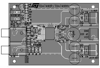
16 Characterization curves Figure 18. Test board () layout 2. Test Board 16/28
17 Package information 5 Package information The comes in a 36-pin PowerSSO package with exposed pad (slug) down. Figure 19 below shows the package outline and Table 6 gives the dimensions. Figure 19. PowerSSO-36 slug down outline drawing h x 45 17/28
18 Package information Table 6. Symbol PowerSSO-36 slug down dimensions Dimensions in mm Dimensions in inch Min Typ Max Min Typ Max A A a b c D E e e F G H h k 0-8 degrees 8 degrees L M N degrees 10 degrees O Q S T U X Y In order to meet environmental requirements, ST offers these devices in ECOPACK packages. These packages have a Pb-free second level interconnect. The category of second Level Interconnect is marked on the package and on the inner box label, in compliance with JEDEC Standard JESD97. The maximum ratings related to soldering conditions are also marked on the inner box label. ECOPACK is an ST trademark. ECOPACK specifications are available at: 18/28
19 Application circuit 6 Application circuit Figure 20. Application circuit Input settings for gain: GAIN0 : GAIN1 Nominal gain 0 V : 0 V 20 db 0 V : 3.3 V 26 db 3.3 V : 0 V 30 db 3.3 V : 3.3 V 32 db Input settings for standby, mute and play: STBY : MUTE Mode 0 V : 0 V Standby 0 V : 3.3 V Standby 3.3 V : 0 V Mute 3.3 V : 3.3 V Play 19/28
20 Application information 7 Application information 7.1 Mode selection The three operating modes of the are set by the two inputs STBY (pin 20) and MUTE (pin 21). Standby mode: all circuits are turned off, very low current consumption. Mute mode: inputs are connected to ground and the positive and negative PWM outputs are at 50% duty cycle. Play mode: the amplifiers are active. The protection functions of the are realized by pulling down the voltages of the STBY and MUTE inputs shown in Figure 21. The input current of the corresponding pins must be limited to 200 µa. Table 7. Mode settings Mode Selection STBY MUTE Standby L (1) Mute H (1) L Play H H 1. Drive levels defined in Table 5: Electrical specifications on page 6 X (don t care) Figure 21. STBY and MUTE circuit 0 V 0 V Standby 3.3 V R2 C7 30 kω 2.2 µf Mute 3.3 V R4 C15 30 kω 2.2 µf STBY MUTE Figure 22. Turn on/off sequence for minimizing speaker pop 20/28
21 Application information 7.2 Gain setting The gain of the is set by the two inputs, GAIN0 (pin 30) and GAIN1 (pin 31). Internally, the gain is set by changing the feedback resistors of the amplifier. Table 8. Gain settings GAIN0 GAIN1 Nominal gain, G v (db) Input resistance and capacitance The input impedance is set by an internal resistor Ri = 60 kω (typical). An input capacitor (Ci) is required to couple the AC input signal. The equivalent circuit and frequency response of the input components are shown in Figure 23. For Ci = 220 nf the high-pass filter cut-off frequency is below 20 Hz: fc = 1 / (2 * π * Ri * Ci) Figure 23. Device input circuit and frequency response Rf Input signal Ci Input pin Ri 21/28
22 Application information 7.4 Internal and external clocks The clock of the class-d amplifier can be generated internally or can be driven by an external source. If two or more class-d amplifiers are used in the same system, it is recommended that all devices operate at the same clock frequency. This can be implemented by using one as master clock, while the other devices are in slave mode (that is, externally clocked. The clock interconnect is via pin SYNCLK of each device. As explained below, SYNCLK is an output in master mode and an input in slave mode Master mode (internal clock) Using the internal oscillator, the output switching frequency, f SW, is controlled by the resistor, R OSC, connected to pin ROSC: f SW = 10 6 / (64 * R OSC + 440) khz where R OSC is in kω. In master mode, pin SYNCLK is used as a clock output pin, whose frequency is: f SYNCLK = 2 * f SW For master mode to operate correctly then resistor R OSC must be less than 60 kω as given below in Table Slave mode (external clock) In order to accept an external clock input the pin ROSC must be left open, that is, floating. This forces pin SYNCLK to be internally configured as an input as given in Table 9. The output switching frequency of the slave devices is: f SW = f SYNCLK / 2 Table 9. How to set up SYNCLK Mode ROSC SYNCLK Master R OSC < 60 kω OUTPUT Slave Floating (not connected) INPUT Figure 24. Master and Slave Connection Master Slave ROSC SYNCLK SYNCLK ROSC Output Input Cosc 100 nf Rosc 39 kω 22/28
23 Application information 7.5 Filterless modulation The output modulation scheme of the BTL is called unipolar pulse width modulation (PWM). The differential output voltages change between zero and +Vcc and between zero and -Vcc. This is in contrast to the traditional bipolar PWM outputs which change between +Vcc and -Vcc. An advantage of this scheme is that it effectively doubles the switching frequency of the differential output waveform. The OUTP and OUTN are in the same phase when the input is zero, then the switching current is low and the loss in the load is small. In practice, a short delay is introduced between these two outputs in order to avoid the BTL output switching at the same time. can be used without a filter before the speaker, because the frequency of the output is beyond the audio frequency, the audio signal can be recovered by the inherent inductance of the speaker and natural filter of the human ear. Figure 25. Unipolar PWM output 23/28
24 Application information 7.6 Output low-pass filter To avoid EMI problems, it may be necessary to use a low-pass filter before the speaker. The cutoff frequency should be larger than 22 khz and much lower than the output switching frequency. It is necessary to choose the L-C component values depending on the loud speaker impedance. Some typical values, which give a cut-off frequency of 27 khz, are shown in Figure 26 and Figure 27 below. Figure 26. Typical LC filter for a 8-Ω speaker Figure 27. Typical LC filter for a 4-Ω speaker 24/28
25 Application information 7.7 Protection function The is fully protected against over-voltages, under-voltages, over- currents and thermal overloads as explained here. See also Table 5: Electrical specifications on page 6. Over voltage protection (OVP) If the supply voltage exceeds 18V (nominal) the over voltage protection is activated which forces the outputs to the high-impedance state. When the supply voltage drops to below the threshold value the device restarts. Under voltage protection (UVP) If the supply voltage drops below 4 V (nominal) the under voltage protection is activated which forces the outputs to the high-impedance state. When the supply voltage recovers the device restarts. Over current protection (OCP) If the output current exceeds 3.5 A (nominal) the over current protection is activated which forces the outputs to the high-impedance state. Periodically, the device attempts to restart. If the over-current condition is still present then the OCP remains active. The restart time, T OC, is determined by the R-C components connected to pin STBY. Thermal protection (OTP) If the junction temperature, T j, reaches 145 C (nominally), the device goes to mute mode and the positive and negative PWM outputs are forced to 50% duty cycle. At Tj = 155 C (nominally), the device shuts down and the output is forced to the high impedance state. When the device cools sufficiently the device restarts. 7.8 Diagnostic output The output pin DIAG is an open drain transistor. When the protection is activated it is in the high-impedance state. The pin can be connected to a power supply (< 18 V) by a pull-up resistor whose value is limited by the maximum sinking current (200 µa) of the pin. Figure 28. Behavior of pin DIAG for various protection conditions VDD R1 DIAG Protection logic VDD Restart Restart Over-current protection OV, UV, OT protection 25/28
26 Application information 7.9 Heatsink requirements A thermal resistance of 24 C/W can be obtained using the PCB copper ground layer with 16 vias connecting it to the contact area for the slug. Ensure that the copper ground area is a nominal 9 cm² for 24 C/W. Figure 29 shows the derating curves for copper areas of 4 cm² and 9 cm². As with most amplifiers, the power dissipated within the device depends primarily on the supply voltage, the load impedance and the output modulation level. The maximum estimated power dissipation for the is less than 2W. When properly mounted on the above PCB the junction temperature could increase by 48 C. However, with a musical program the dissipated power is about 40% less, leading to a temperature increase of around 30 C. Even at the maximum recommended ambient temperature for consumer applications of 50 C there is still a clear safety margin before the maximum junction temperature (150 C) is reached. Figure 29. Pd (W) Power derating curves for PCB used gas heatsink 8 7 Copper Area 3x3 cm 6 and via holes Copper Area 2x2 cm 2 and via holes Tamb ( C) TDA7491P PSSO36 PSSO-36 26/28
27 Revision history 8 Revision history Table 10. Document revision history Date Revision Changes 02-Jul Initial release. 20-Oct Characterization curves updated. 27/28
28 Please Read Carefully: Information in this document is provided solely in connection with ST products. STMicroelectronics NV and its subsidiaries ( ST ) reserve the right to make changes, corrections, modifications or improvements, to this document, and the products and services described herein at any time, without notice. All ST products are sold pursuant to ST s terms and conditions of sale. Purchasers are solely responsible for the choice, selection and use of the ST products and services described herein, and ST assumes no liability whatsoever relating to the choice, selection or use of the ST products and services described herein. No license, express or implied, by estoppel or otherwise, to any intellectual property rights is granted under this document. If any part of this document refers to any third party products or services it shall not be deemed a license grant by ST for the use of such third party products or services, or any intellectual property contained therein or considered as a warranty covering the use in any manner whatsoever of such third party products or services or any intellectual property contained therein. UNLESS OTHERWISE SET FORTH IN ST S TERMS AND CONDITIONS OF SALE ST DISCLAIMS ANY EXPRESS OR IMPLIED WARRANTY WITH RESPECT TO THE USE AND/OR SALE OF ST PRODUCTS INCLUDING WITHOUT LIMITATION IMPLIED WARRANTIES OF MERCHANTABILITY, FITNESS FOR A PARTICULAR PURPOSE (AND THEIR EQUIVALENTS UNDER THE LAWS OF ANY JURISDICTION), OR INFRINGEMENT OF ANY PATENT, COPYRIGHT OR OTHER INTELLECTUAL PROPERTY RIGHT. UNLESS EXPRESSLY APPROVED IN WRITING BY AN AUTHORIZED ST REPRESENTATIVE, ST PRODUCTS ARE NOT RECOMMENDED, AUTHORIZED OR WARRANTED FOR USE IN MILITARY, AIR CRAFT, SPACE, LIFE SAVING, OR LIFE SUSTAINING APPLICATIONS, NOR IN PRODUCTS OR SYSTEMS WHERE FAILURE OR MALFUNCTION MAY RESULT IN PERSONAL INJURY, DEATH, OR SEVERE PROPERTY OR ENVIRONMENTAL DAMAGE. ST PRODUCTS WHICH ARE NOT SPECIFIED AS "AUTOMOTIVE GRADE" MAY ONLY BE USED IN AUTOMOTIVE APPLICATIONS AT USER S OWN RISK. Resale of ST products with provisions different from the statements and/or technical features set forth in this document shall immediately void any warranty granted by ST for the ST product or service described herein and shall not create or extend in any manner whatsoever, any liability of ST. ST and the ST logo are trademarks or registered trademarks of ST in various countries. Information in this document supersedes and replaces all information previously supplied. The ST logo is a registered trademark of STMicroelectronics. All other names are the property of their respective owners STMicroelectronics - All rights reserved STMicroelectronics group of companies Australia - Belgium - Brazil - Canada - China - Czech Republic - Finland - France - Germany - Hong Kong - India - Israel - Italy - Japan - Malaysia - Malta - Morocco - Singapore - Spain - Sweden - Switzerland - United Kingdom - United States of America 28/28
Description. Order code Operating Temp. range Package Packing
 20 W + 20 W dual BTL class-d audio amplifier Features! 20 W + 20 W continuous output power: R L = 8 Ω, THD = 10% at V CC = 18 V! Wide range single supply operation (5 V - 18 V)! High efficiency (η = 90%)!
Description. Order code Operating Temp. range Package Packing
 10 W + 10 W dual BTL class-d audio amplifier Features 10 W + 10 W continuous output power: R L = 6 Ω, THD = 10% at V CC = 11 V 9.5 W + 9.5 W continuous output power: R L = 8 Ω, THD = 10% at V CC = 12 V
Description. Order code Operating temp. range Package Packaging
 100 watt + 100 watt dual BTL class-d audio amplifier Features 100 W + 100 W output power at THD = 10% with R L = 6 Ω and V CC = 36 V 80 W + 80 W output power at THD = 10% with R L = 8 Ω and V CC = 34 V
TDA7498L. 80-watt + 80-watt dual BTL class-d audio amplifier. Description. Features
 80-watt + 80-watt dual BTL class-d audio amplifier Datasheet - production data Differential inputs minimize common-mode noise Standby and mute features Short-circuit protection Thermal overload protection
Description. Order code Operating temp. range Package Packaging
 25-watt + 25-watt dual BTL class-d audio amplifier Features 25 W + 25 W continuous output power at THD = 10% with V CC = 20 V and R L = 8 Ω Wide-range single-supply operation (8-26 V) High efficiency (η
Description. Order code Operating temp. range Package Packaging
 160-watt + 160-watt dual BTL class-d audio amplifier Preliminary data Features 160-W + 160-W output power at THD = 10% with R L = 4 Ω and V CC = 36 V 1 x 220 W output power mono parallel BTL at THD = 10%
Description. Order code Operating temp. range Package Packaging
 00-watt + 00-watt dual BTL class-d audio amplifier Features 00-W + 00-W output power at THD = 0% with R L = 6 Ω and V CC = 36 V 80-W + 80-W output power at THD = 0% with R L = 8 Ω and V CC = 34 V Wide-range
Description. Table 1. Device summary. Order code Operating temp. range Package Packaging
 TDA7492PE 45 W + 45 W dual BTL class-d audio amplifier Datasheet - production data Features Wide-range single-supply operation (9-26 V) Possible output configurations: 2 x PBTL 1 x Parallel BTL BTL output
Description. Order code Temperature range Package Packaging
 80 watt + 80 watt dual BTL class-d audio amplifier Features 80 W + 80 W output power at THD = 0% with R L = 6 Ω and V CC = 32 V 70 W + 70 W output power at THD = 0% with R L = 8 Ω and V CC = 34 V Wide-range
Obsolete Product(s) - Obsolete Product(s)
 - Obsolete Product(s)") 2 W mono amplifier Features 2 W output power into 8 Ω at 12 V, THD = 10% Internally fixed gain of 32 db No feedback capacitor No boucherot cell Thermal protection AC short-circuit protection SVR capacitor
2 W mono amplifier Features 2 W output power into 8 Ω at 12 V, THD = 10% Internally fixed gain of 32 db No feedback capacitor No boucherot cell Thermal protection AC short-circuit protection SVR capacitor
Obsolete Product(s) - Obsolete Product(s)
 - Obsolete Product(s)") Low drop - Low supply voltage Low ESR capacitor compatible Feature summary Input voltage from 1.7 to 3.6V Ultra low dropout voltage (130mV typ. at 300mA load) Very low quiescent current (110µA typ. at
Low drop - Low supply voltage Low ESR capacitor compatible Feature summary Input voltage from 1.7 to 3.6V Ultra low dropout voltage (130mV typ. at 300mA load) Very low quiescent current (110µA typ. at
LM723CN. High precision voltage regulator. Features. Description
 High precision voltage regulator Features Input voltage up to 40 V Output voltage adjustable from 2 to 37 V Positive or negative supply operation Series, shunt, switching or floating operation Output current
Low noise low drop voltage regulator with shutdown function. Part numbers
 Low noise low drop voltage regulator with shutdown function Features Output current up to 150 ma Low dropout voltage (350 mv at I OUT = 50 ma) Very low quiescent current: 0.1 µa in OFF mode and max. 250
KF25B, KF33B KF50B, KF80B
 KF25B, KF33B KF50B, KF80B Very low drop voltage regulators with inhibit Datasheet production data Features Very low dropout voltage (0.4 V) Very low quiescent current (typ. 50 µa in OFF mode, 500 µa in
L4940xx5 L4940V5 L4940D2T5-TR 5 V L4940xx85 L4940V85 L4940P85 L4940D2T85-TR 8.5 V L4940xx10 L4940D2T10-TR 10 V L4940xx12 L4940D2T12-TR 12 V
 Very low drop 1.5 A regulator Features Precise 5, 8.5, 10, 12 V outputs Low dropout voltage (450 mv typ. at 1 A) Very low quiescent current Thermal shutdown Short circuit protection Reverse polarity protection
LF253 LF353. Wide bandwidth dual JFET operational amplifiers. Features. Description
 Wide bandwidth dual JFET operational amplifiers Features Low power consumption Wide common-mode (up to V CC + ) and differential voltage range Low input bias and offset current Output short-circuit protection
TDA W W dual BTL class-d audio amplifier. Features. Description. R L =4Ω, THD = 10%, Vcc = 5 V. 6 db, 12 db, 15.6 db and 18 db.
 2.8 W + 2.8 W dual BTL class-d audio amplifier Features! 2.8 W + 2.8 W continuous output power R L =4Ω, THD = 10%, Vcc = 5 V! Single supply voltage range 4.5 V to 5.5 V! High efficiency (η = 83%)! Four
Obsolete Product(s) - Obsolete Product(s)
 - Obsolete Product(s)") 10 W car radio audio amplifier Datasheet production data Features Improved performance over the TDA2002 (pinto-pin compatible) Very low number of external components Ease of assembly Cost and space savings
10 W car radio audio amplifier Datasheet production data Features Improved performance over the TDA2002 (pinto-pin compatible) Very low number of external components Ease of assembly Cost and space savings
ST619LBDR. DC-DC converter regulated 5 V charge pump. Features. Description
 DC-DC converter regulated 5 V charge pump Features Regulated 5 V ±4 % charge pump Output current guaranteed over temperature: 20 ma (V I 2 V), 30 ma (V I 3 V) No inductors; very low EMI noise Uses small,
LD1085CXX. 3 A low-drop, adjustable positive voltage regulator. Features. Description
 3 A low-drop, adjustable positive voltage regulator Features Typical dropout 1.3 V (at 3 A) Three terminal adjustable output voltage Guaranteed output current up to 3 A Output tolerance ± 2 % at 25 C and
MC33172 MC Low power dual bipolar operational amplifiers. Features. Description
 Low power dual bipolar operational amplifiers Features Good consumption/speed ratio: only 200 µa for 2.1MHz, 2V/µs Single (or dual) supply operation from +4 V to +44V (±2V to ±22V) Wide input common mode
TDA W hi-fi audio amplifier. Features. Description
 TDA2030 14 W hi-fi audio amplifier Features Wide-range supply voltage, up to 36 V Single or split power supply Short-circuit protection to ground Thermal shutdown Description The TDA2030 is a monolithic
AN3385 Application note
 Application note 50 W + 50 W dual BTL class-d audio amplifier demonstration board based on the TDA7492 Introduction This application note describes the STEVAL-CCA027V1 demonstration board designed for
L79xxC. Negative voltage regulators. Features. Description
 Negative voltage regulators Features Output current up to 1.5 A Output voltages of -5; -8; -12; -15; -20 V Thermal overload protection Short circuit protection Output transition SOA protection Description
LM323. Three-terminal 3 A adjustable voltage regulators. Features. Description
 Three-terminal 3 A adjustable voltage regulators Features Output current: 3 A Internal current and thermal limiting Typical output impedance: 0.01 W Minimum input voltage: 7.5 V Power dissipation: 30 W
BD241A BD241C. NPN power transistors. Features. Applications. Description. NPN transistors. Audio, general purpose switching and amplifier transistors
 BD241A BD241C NPN power transistors Features. NPN transistors Applications Audio, general purpose switching and amplifier transistors Description The devices are manufactured in Planar technology with
Obsolete Product(s) - Obsolete Product(s) Obsolete Product(s) - Obsolete Product(s)
 - Obsolete Product(s) Obsolete Product(s) - Obsolete Product(s)") 5 A low dropout fast response positive voltage regulator adjustable Features Typical dropout 1.2 V Fast transient response Three terminal adjustable Guaranteed output current up to 5 A Output tolerance
5 A low dropout fast response positive voltage regulator adjustable Features Typical dropout 1.2 V Fast transient response Three terminal adjustable Guaranteed output current up to 5 A Output tolerance
LK115XX30 LK115XX33 - LK115XX50
 LK115XX30 LK115XX33 - LK115XX50 ery low drop with inhibit voltage regulators Features ery low dropout voltage (0.2 typ.) ery low quiescent current (Typ. 0.01 µa in off mode, 280 µa in on mode) Output current
TDA7233D 1W AUDIO AMPLIFIER WITH MUTE
 1 AUDIO AMPLIFIER ITH MUTE 1 FEATURES OPERATING VOLTAGE 1.8 TO 15 V EXTERNAL MUTE OR POER DON FUNCTION IMPROVED SUPPLY VOLTAGE REJECTION LO QUIESCENT CURRENT HIGH POER CAPABILITY LO CROSSOVER DISTORTION
Obsolete Product(s) - Obsolete Product(s)
 - Obsolete Product(s)") High gain Low Voltage PNP power transistor Features Very low Collector to Emitter saturation voltage D.C. Current gain, h FE >100 1.5 A continuous collector current Applications Power management in portable
High gain Low Voltage PNP power transistor Features Very low Collector to Emitter saturation voltage D.C. Current gain, h FE >100 1.5 A continuous collector current Applications Power management in portable
Description. Order code Operating temp. range Package Packaging. TDA to 70 C Multiwatt11 Tube +V S. 1000μF
 40 W + 40 W stereo amplifier with mute and standby Datasheet production data Features Wide supply voltage range (up to ± 33 V) Split supply High output power 40 W + 40 W into 8 Ω with V S = ±26 V and THD
STD1802T4-A. Low voltage fast-switching NPN power transistor. Features. Description. Applications
 Low voltage fast-switching NPN power transistor Features This device is qualified for automotive application Very low collector to emitter saturation voltage High current gain characteristic Fast-switching
2STN2540. Low voltage fast-switching PNP power bipolar transistor. Features. Applications. Description
 2STN2540 Low voltage fast-switching PNP power bipolar transistor Features Very low collector-emitter saturation voltage High current gain characteristic Fast switching speed Surface mounting device in
LF253, LF353. Wide bandwidth dual JFET operational amplifiers. Features. Description
 Wide bandwidth dual JFET operational amplifiers Features Low power consumption Wide common-mode (up to + ) and differential voltage range Low input bias and offset current Output short-circuit protection
Low noise low drop voltage regulator with shutdown function. Part numbers
 Low noise low drop voltage regulator with shutdown function Features Output current up to 150 ma Low dropout voltage (350 mv at I OUT = 50 ma) Very low quiescent current: 0.1 µa in OFF mode and max. 250
2STC4468. High power NPN epitaxial planar bipolar transistor. Features. Application. Description
 High power NPN epitaxial planar bipolar transistor Features High breakdown voltage V CEO = 140 V Complementary to 2STA1695 Typical f t = 20 MHz Fully characterized at 125 o C Application Audio power amplifier
2STA1943. High power PNP epitaxial planar bipolar transistor. Features. Application. Description
 High power PNP epitaxial planar bipolar transistor Features High breakdown voltage V CEO > -230V Complementary to 2STC5200 Fast-switching speed Typical f T = 30 MHz Application Audio power amplifier Description
LD3985xx. Ultra low drop-low noise BiCMOS voltage regulators low ESR capacitors compatible. Features. Description
 Ultra low drop-low noise BiCMOS voltage regulators low ESR capacitors compatible Features Input voltage from 2.5 V to 6 V Stable with low ESR ceramic capacitors Ultra low dropout voltage (100 mv typ. at
STCS05A. 0.5 A max constant current LED driver. Features. Applications. Description
 0.5 A max constant current LED driver Features Up to 40 V input voltage Less than 0.5 V voltage overhead Up to 0.5 A output current PWM dimming pin Shutdown pin LED disconnection diagnostic Slope control
TDA W + 3 W dual BTL class-d audio amplifier. Features. Description
 3 W + 3 W dual BTL class-d audio amplifier Features 3.0 W + 3.0 W continuous output power R L =4Ω, THD = 10%, V CC = 5 V (filterless) 2.8 W + 2.8 W continuous output power R L =4Ω, THD = 10%, V CC = 5
TS522. Precision low noise dual operational amplifier. Features. Description
 Precision low noise dual operational amplifier Datasheet production data Features Large output voltage swing: +14.3 V/-14.6 V Low input offset voltage 850 μv max. Low voltage noise: 4.5 nv/ Hz High gain
MC Low noise quad operational amplifier. Features. Description
 MC3379 Low noise quad operational amplifier Features Low voltage noise: 4.5 nv/ Hz High gain bandwidth product: 15 MHz High slew rate: 7 V/µs Low distortion:.2% Large output voltage swing: +14.3 V/-14.6
L78M00 series. Positive voltage regulators. Feature summary. Description. Schematic diagram
 Positive voltage regulators Feature summary Output current to 0.5A Output voltages of 5; 6; 8; 9; 10; 12; 15; 18; 20; 24V Thermal overload protection Short circuit protection Output transition SOA protection
2STC5242. High power NPN epitaxial planar bipolar transistor. Features. Application. Description
 2STC5242 High power NPN epitaxial planar bipolar transistor Features High breakdown voltage V CEO = 230 V Complementary to 2STA1962 Fast-switching speed Typical f T = 30 MHz Application Audio power amplifier
STCS2. 2 A max constant current LED driver. Features. Applications. Description
 2 A max constant current LED driver Features Up to 40 V input voltage Less than 0.5 V voltage overhead Up to 2 A output current PWM dimming pin Shutdown pin LED disconnection diagnostic 10 1 PowerSO-10
L78S00 series. 2A Positive voltage regulators. Feature summary. Description. Schematic diagram
 2A Positive voltage regulators Feature summary Output current to 2A Output voltages of 5; 7.5; 9; 10; 12; 15; 18; 24V Thermal overload protection Short circuit protection Output transition SOA protection
BD533 BD535 BD537 BD534 BD536
 BD533 BD535 BD537 BD534 BD536 Complementary power transistors Features. BD533, BD535, and BD537 are NPN transistors Description The devices are manufactured in Planar technology with Base Island layout.
Part numbers Order codes Packages Temperature range. LM137 LM137K TO-3-55 C to 150 C LM337 LM337K TO-3 0 C to 125 C LM337 LM337SP TO C to 125 C
 LM137 LM337 Three-terminal adjustable negative voltage regulators Features Output voltage adjustable down to V REF 1.5 A guaranteed output current 0.3%/V typical load regulation 0.01%/V typical line regulation
LS1240. Electronic two-tone ringer. Features. Description. Pin connection (top view)
") Electronic two-tone ringer Features Low current consumption, in order to allow the parallel operation of 4 devices Integrated rectifier bridge with zener diodes to protect against over voltages little
Electronic two-tone ringer Features Low current consumption, in order to allow the parallel operation of 4 devices Integrated rectifier bridge with zener diodes to protect against over voltages little
 Distributed by: www.jameco.com 1-800-831-4242 The content and copyrights of the attached material are the property of its owner. 1.5A Low drop positive voltage regulator adjustable and fixed Feature summary
Obsolete Product(s) - Obsolete Product(s)
 - Obsolete Product(s)") P-channel 20V - 0.065Ω - 4.2A - SOT-223 2.5V - Drive STripFET II Power MOSFET General features Type V DSS R DS(on) I D STN5PF02V 20V
P-channel 20V - 0.065Ω - 4.2A - SOT-223 2.5V - Drive STripFET II Power MOSFET General features Type V DSS R DS(on) I D STN5PF02V 20V
Description. Part numbers Order codes Packages Output voltages
 LDFM LDFM5 5 ma very low drop voltage regulator Datasheet production data Features Input voltage from 2.5 to 16 V Very low dropout voltage (3 mv max. at 5 ma load) Low quiescent current (2 µa typ. @ 5
Obsolete Product(s) - Obsolete Product(s)
 - Obsolete Product(s)") High power PNP epitaxial planar bipolar transistor Features High breakdown voltage V CEO = -250 V Complementary to 2STC5949 Typical f t = 25 MHz Fully characterized at 125 o C Application Audio power amplifier
High power PNP epitaxial planar bipolar transistor Features High breakdown voltage V CEO = -250 V Complementary to 2STC5949 Typical f t = 25 MHz Fully characterized at 125 o C Application Audio power amplifier
ST662AB ST662AC. DC-DC converter from 5 V to 12 V, 0.03 A for Flash memory programming supply. Features. Description
 ST662AB ST662AC DC-DC converter from 5 V to 12 V, 0.03 A for Flash memory programming supply Features Output voltage: 12 V ± 5 % Supply voltage range: 4.5 V to 5.5 V Guaranteed output current up to 30
STGE200NB60S. N-channel 150A - 600V - ISOTOP Low drop PowerMESH IGBT. General features. Description. Internal schematic diagram.
 N-channel 150A - 600V - ISOTOP Low drop PowerMESH IGBT General features TYPE V CES V CE(sat) (typ.) I C T C 600V 1.2V 1.3V 150A 200A 100 C 25 C High input impedance (voltage driven) Low on-voltage drop
Order codes Marking Package Packaging. STD2805T4 D2805 DPAK Tape & reel STD D2805 IPAK Tube. June 2007 Rev 1 1/9
 Low voltage fast-switching PNP power transistor Preliminary Data Features Very low collector to emitter saturation voltage High current gain characteristic Fast-switching speed Surface-mounting DPAK (TO-252)
Obsolete Product(s) - Obsolete Product(s)
 - Obsolete Product(s)") Low power quad operational amplifier Features Wide gain bandwidth: 1.3 MHz Extended temperature range: -40 C to +150 C Input common-mode voltage range includes negative rail Large voltage gain: 100 db
Low power quad operational amplifier Features Wide gain bandwidth: 1.3 MHz Extended temperature range: -40 C to +150 C Input common-mode voltage range includes negative rail Large voltage gain: 100 db
L9473 Car alternator voltage regulator Features Description
 Car alternator voltage regulator Features For air and liquid cooled applications Ambient air temperature (thermistor) compensated Special default compensation curve with TSterminal open Compensation curve
L6234. Three phase motor driver. Features. Description
 Three phase motor driver Features Supply voltage from 7 to 52 V 5 A peak current R DSon 0.3 Ω typ. value at 25 C Cross conduction protection TTL compatible driver Operating frequency up to 150 khz Thermal
Obsolete Product(s) - Obsolete Product(s)
 - Obsolete Product(s)") High Gain Low Voltage PNP Power Transistor General features Very low Collector to Emitter saturation voltage D.C. Current gain, h FE >100 1.5 A continuous collector current In compliance with the 2002/93/EC
High Gain Low Voltage PNP Power Transistor General features Very low Collector to Emitter saturation voltage D.C. Current gain, h FE >100 1.5 A continuous collector current In compliance with the 2002/93/EC
2STX2220. High Gain Low Voltage PNP Power Transistor. General features. Description. Internal schematic diagram. Applications.
 High Gain Low Voltage PNP Power Transistor General features Very low Collector to Emitter saturation voltage D.C. Current gain, h FE >100 1.5 A continuous collector current In compliance with the 2002/93/EC
TO-220 D²PAK TO-220FP
 Negative voltage regulators Datasheet production data Features Output current up to 1.5 A Output voltages of - 5; - 8; - 12; - 15 V Thermal overload protection Short circuit protection Output transition
LDS3985xx. Ultra low drop-low noise BiCMOS 300 ma voltage regulator for use with very low ESR output capacitor. Features.
 Ultra low drop-low noise BiCMOS 300 ma voltage regulator for use with very low ESR output capacitor Features Input voltage from 2.5 V to 6 V Stable with low ESR ceramic capacitors Ultra low dropout voltage
Order codes Marking Package Packaging 2STF SOT-89 2STN2550 N2550 SOT-223. November 2008 Rev 1 1/8
 2STF2550 2STN2550 Low voltage high performance PNP power transistors Preliminary Data Features Very low collector-emitter saturation voltage High current gain characteristic Fast switching speed Surface
Obsolete Product(s) - Obsolete Product(s)
 - Obsolete Product(s)") High voltage fast-switching NPN Power transistor General features High voltage and high current capability Low spread of dynamic parameters Low base-drive requirements Very high switching speed High ruggedness
High voltage fast-switching NPN Power transistor General features High voltage and high current capability Low spread of dynamic parameters Low base-drive requirements Very high switching speed High ruggedness
STB High voltage fast-switching NPN power transistor. Features. Applications. Description
 High voltage fast-switching NPN power transistor Features Low spread of dynamic parameters Minimum lot-to-lot spread for reliable operation Very high switching speed Through hole TO-262 (I 2 PAK) power
Obsolete Product(s) - Obsolete Product(s)
 - Obsolete Product(s)") Three-terminal 5 A adjustable voltage regulators Features Guaranteed 7 A peak output current Guaranteed 5 A output current Adjustable output down to 1.2 V Line regulation typically 0.005 %/V Load regulation
Three-terminal 5 A adjustable voltage regulators Features Guaranteed 7 A peak output current Guaranteed 5 A output current Adjustable output down to 1.2 V Line regulation typically 0.005 %/V Load regulation
Order codes Temperature range Package Packaging
 CMOS quad 3-state differential line receiver Features CMOS design for low power ± 0.2 V sensitivity over input common mode voltage range Typical propagation delay: 19 ns Typical input hysteresis: 60 mv
STB160N75F3 STP160N75F3 - STW160N75F3
 STB160N75F3 STP160N75F3 - STW160N75F3 N-channel 75V - 3.5mΩ - 120A - TO-220 - TO-247 - D 2 PAK STripFET Power MOSFET Features Type V DSS R DS(on) (max.) I D STB160N75F3 75V 3.7 mω 120 A (1) STP160N75F3
Obsolete Product(s) - Obsolete Product(s)
 - Obsolete Product(s)") Single bilateral switch Features High speed: t PD = 0.3 ns (typ.) at V CC = 5 V t PD = 0.4 ns (typ.) at V CC = 3.3 V Low power dissipation: I CC = 1 μa (max.) at T A =25 C Low "ON" resistance: R ON =6.5Ω
Single bilateral switch Features High speed: t PD = 0.3 ns (typ.) at V CC = 5 V t PD = 0.4 ns (typ.) at V CC = 3.3 V Low power dissipation: I CC = 1 μa (max.) at T A =25 C Low "ON" resistance: R ON =6.5Ω
LD1117Axx. Low drop fixed and adjustable positive voltage regulators. Features. Description
 Low drop fixed and adjustable positive voltage regulators Features Low dropout voltage (1.15 V typ. @ I OUT = 1 A, 25 C) Very low quiescent current (5 ma typ. @ 25 C) Output current up to 1 A Fixed output
BUL39D. High voltage fast-switching NPN power transistor. Features. Application. Description
 High voltage fast-switching NPN power transistor Features Integrated antiparallel collector-emitter diode High voltage capability Low spread of dynamic parameters Minimum lot-to-lot spread for reliable
2ST2121. High power PNP epitaxial planar bipolar transistor. Features. Applications. Description 1 2 TO-3
 High power PNP epitaxial planar bipolar transistor Features High breakdown voltage V CEO = -250 V Complementary to 2ST5949 Typical f t = 25 MHz Fully characterized at 125 o C Applications Audio power amplifier
BD243C BD244C. Complementary power transistors. Features. Applications. Description. Complementary NPN-PNP devices. Power linear and switching TO-220
 BD243C BD244C Complementary power transistors Features. Complementary NPN-PNP devices Applications Power linear and switching Description The device is manufactured in Planar technology with Base Island
LD39150xx Ultra low drop BiCMOS voltage regulator Features Description Typical application
 Ultra low drop BiCMOS voltage regulator Features 1.5 A guaranteed output current Ultra low dropout voltage (200 mv typ. @ 1.5 A load, 40 mv typ. @ 300 ma load) Very low quiescent current (1 ma typ. @ 1.5
L6932H1.2. High performance 2A ULDO linear regulator. Features. Description. Applications L6932H1.2
 High performance 2A ULDO linear regulator Features 2V to 14V input voltage range 200mΩ r DS(on) max 200µA quiescent current at any load Excellent load and line regulation Adjustable from 1.2V to 5V 1%
HCF4093. QUAD 2-input NAND Schmidt trigger. Features. Description
 QUAD 2-input NAND Schmidt trigger Features Schmidt trigger action on each input with no external components Hysteresis voltage typically 0.9 V at V DD =5V and 2.3 V at V DD =10 V Noise immunity greater
2STD1665. Low voltage fast-switching NPN power transistor. Features. Applications. Description
 Low voltage fast-switching NPN power transistor Features Very low collector to emitter saturation volatage High current gain characteristic Fast-switching speed Through-hole IPAK (TO-251) power package
2N7000 2N7002. N-channel 60V - 1.8Ω A - SOT23-3L / TO-92 STripFET Power MOSFET. General features. Description. Internal schematic diagram
 2N7000 2N7002 N-channel 60V - 1.8Ω - 0.35A - SOT23-3L / TO-92 STripFET Power MOSFET General features Type V DSS R DS(on) I D 2N7000 60V
Obsolete Product(s) - Obsolete Product(s)
 - Obsolete Product(s)") N-channel 30V - 0.020Ω - 6A - TSSOP8 2.5V-drive STripFET II Power MOSFET General features Type V DSS R DS(on) I D 30V < 0.025 Ω (@ 4.5 V) < 0.030 Ω (@ 2.7 V) 6A Ultra low threshold gate drive (2.5V) Standard
N-channel 30V - 0.020Ω - 6A - TSSOP8 2.5V-drive STripFET II Power MOSFET General features Type V DSS R DS(on) I D 30V < 0.025 Ω (@ 4.5 V) < 0.030 Ω (@ 2.7 V) 6A Ultra low threshold gate drive (2.5V) Standard
EMIF01-SMIC01F2. Single line IPAD, EMI filter including ESD protection. Features. Application. Description. Complies with the following standards
 Single line IPAD, EMI filter including ESD protection Features High density capacitor 1 line low-pass-filter Lead-free package High efficiency in EMI filtering Very low PCB space consumtion Very thin package:
2STA1695. High power PNP epitaxial planar bipolar transistor. Features. Applications. Description
 High power PNP epitaxial planar bipolar transistor Features High breakdown voltage V CEO = -140 V Complementary to 2STC4468 Typical f t = 20 MHz Fully characterized at 125 C Applications 1 2 3 Audio power
2STR SOT-23 Tape and reel 2STR1230G 130G SOT-23 Tape and reel
 Low voltage fast-switching NPN power transistor Features Very low collector-emitter saturation voltage High current gain characteristic Fast switching speed Miniature SOT-23 plastic package for surface
Obsolete Product(s) - Obsolete Product(s)
 - Obsolete Product(s)") General features Supply voltage range: 2.6V to 5.5V 17V Maximum output voltage STCF01 Step-up converter for cell phone camera flash LEDs Two current levels up to 300mA set with external resistors Dedicated
General features Supply voltage range: 2.6V to 5.5V 17V Maximum output voltage STCF01 Step-up converter for cell phone camera flash LEDs Two current levels up to 300mA set with external resistors Dedicated
TS3704. Micropower quad CMOS voltage comparators. Features. Description
 Micropower quad CMOS voltage comparators Features Push-pull CMOS output (no external pull-up resistor required) Extremely low supply current: 9μa typ per comparator Wide single supply range 2.7V to 6V
DB Evaluation board using PD85004 for 900 MHz 2-way radio. Features. Description
 Evaluation board using PD85004 for 900 MHz 2-way radio Features Excellent thermal stability Frequency: 860-960 MHz Supply voltage: 13.6 V Output power: 4 W Power gain: 17.4 ± 0.3 db Efficiency: 56 % -
High voltage NPN Power transistor for standard definition CRT display. R BE =60Ω typ. Order code Marking Package Packing
 High voltage NPN Power transistor for standard definition CRT display Features State-of-the-art technology: Diffused collector enhanced generation Stable performance versus operating temperature variation
STP14NF10. N-channel 100 V Ω - 15 A - TO-220 low gate charge STripFET II Power MOSFET. Features. Application. Description
 N-channel 100 V - 0.115 Ω - 15 A - TO-220 low gate charge STripFET II Power MOSFET Features Type V DSS R DS(on) max I D STP14NF10 100 V < 0.13 Ω 15 A Exceptional dv/dt capability 100% avalanche tested
TDA x 41 W quad bridge car radio amplifier. Features. Description. Protections:
 4 x 41 W quad bridge car radio amplifier Features High output power capability: 4 x 41 W / 4 Ω max. 4 x 26 W / 4 Ω @ 14.4 V, 1 khz, 10 % Low distortion Low output noise Standby function Mute function Automute
SD1728 (TH430) RF & Microwave transistors HF SSB application. Features. Description. Pin connection
 RF & Microwave transistors HF SSB application. Features. Description. Pin connection") SD1728 (TH430) RF & Microwave transistors HF SSB application Features 13.56MHz 44V Gold metallization Common emitter P OUT = 200W with 15dB gain Description The SD1728 is a 50V epitaxial silicon NPN planar
SD1728 (TH430) RF & Microwave transistors HF SSB application Features 13.56MHz 44V Gold metallization Common emitter P OUT = 200W with 15dB gain Description The SD1728 is a 50V epitaxial silicon NPN planar
Obsolete Product(s) - Obsolete Product(s)
 - Obsolete Product(s)") PNP power Darlington transistor Features Monolithic Darlington configuration Integrated antiparallel collector-emitter diode Application Linear and switching industrial equipment Description The TIP145
PNP power Darlington transistor Features Monolithic Darlington configuration Integrated antiparallel collector-emitter diode Application Linear and switching industrial equipment Description The TIP145
Obsolete Product(s) - Obsolete Product(s)
 - Obsolete Product(s)") Low voltage fast-switching PNP power transistor Features Very low collector-emitter saturation voltage High current gain characteristic Fast switching speed 3 Miniature SOT-23 plastic package for surface
Low voltage fast-switching PNP power transistor Features Very low collector-emitter saturation voltage High current gain characteristic Fast switching speed 3 Miniature SOT-23 plastic package for surface
2STR2215. Low voltage fast-switching PNP power transistor. Features. Applications. Description
 Low voltage fast-switching PNP power transistor Features Very low collector-emitter saturation voltage High current gain characteristic Fast switching speed Miniature SOT-23 plastic package for surface
BUV298V. NPN transistor power module. General features. Applications. Internal schematic diagram. Order codes
 NPN transistor power module General features NPN Transistor High current power bipolar module Very low R th junction case Specific accidental overload areas Fully insulated package (U.L. compliant) for
Order codes Temperature range Package Packaging
 CMOS quad 3-state differential line driver Features TTL input compatible Typical propagation delay: 6 ns Typical output skew: 0.5 ns Output will not load line when V CC = 0 V Meets the requirements of
BD235 BD237. Low voltage NPN power transistors. Features. Applications. Description. Low saturation voltage NPN transistors
 BD235 BD237 Low voltage NPN power transistors Features Low saturation voltage NPN transistors Applications Audio, power linear and switching applications Description The devices are manufactured in Planar
MD1802FX. High voltage NPN power transistor for standard definition CRT display. Features. Applications. Description
 High voltage NPN power transistor for standard definition CRT display Features State-of-the-art technology: Diffused collector Enhanced generation Stable performances versus operating temperature variation
STN9260. High voltage fast-switching PNP power transistor. Features. Applications. Description. High voltage capability Fast switching speed
 High voltage fast-switching PNP power transistor Features High voltage capability Fast switching speed Applications Lighting Switch mode power supply Description This device is a high voltage fast-switching
STD30NF03L STD30NF03L-1
 STD30NF03L STD30NF03L-1 N-channel 30V - 0.020Ω - 30A - DPAK/IPAK STripFET II Power MOSFET General features Type V DSS R DS(on) I D STD30NF03L-1 30V < 0.025Ω 30A STD30NF03L 30V < 0.025Ω 30A Low threshold
MD2103DFH. High voltage NPN power transistor for standard definition CRT display. Features. Description. Applications
 High voltage NPN power transistor for standard definition CRT display Features State-of-the-art technology: Diffused collector enhanced generation Stable performance versus operating temperature variation