SY58626L. General Description. Features. Applications
|
|
|
- Lambert Haynes
- 6 years ago
- Views:
Transcription
1 DC-to-6.4Gbps Backplane Transmit Buffer with Selectable Output Pre-emphasis, I/O DC-Offset Control, and 200mV-3.0V PP Output Swing General Description The high-speed, low jitter transmit buffer is optimized for backplane and transmission line data-path management applications in Automatic Test Equipment (ATE) and Test & Measurement (T&M) systems. The buffer includes a CML compatible, variable swing output with selectable pre-emphasis. The is capable of driving serial data from DC through 6.4Gbps with a 3V PP (1.5V PK single ended) differential swing. The differential input includes Micrel s unique, 3-pin input termination architecture that directly interfaces to any DC- or AC-coupled, differential signal as small as 100mV PK without any termination resistor networks in the signal path. The outputs are 50Ω source-terminated CML with a programmable output swing from 200mV PP to 3V PP (100mV PK to 1.5V PK ). The includes an output stage that provides 4 levels of pre-emphasis. The output pre-emphasis level is programmed with a three-bit interface. Unlike other transmitter solutions, the output pre-emphasis duration can be programmed from 60ps to 400ps. The operates at 3.3V ±10% supply and is guaranteed over the commercial temperature range of 0 C to +70 C. The transmitter is optimized to work with the SY58627L receiver. The is part of Micrel s high-speed, Precision Edge product line. Data sheets and support documentation can be found on Micrel s website at: Features Precision Edge Transmit driver provides output pre-emphasis to extend transmission range 4 selectable pre-emphasis levels Drives 6.4Gbps up to 12 FR4 PCB trace, or longer combinations of FR4+cable+interconnect DC through 6.4Gbps data rate throughput Integrated loopback capability Unique pre-emphasis: - Programmable pre-emphasis magnitude - Programmable pre-emphasis duration Unique, flexible I/O: - Internal termination to VTTIN pin interfaces to any differential AC- or DC-coupled signals - 50Ω source terminated CML outputs minimize round-trip reflections - Programmable output swing control: 200mV- 3.0V PP - Output Disable and output shutdown - DC-offset control with VTT I/O 3.3V ±10% supply voltage 0 C to +70 C temperature range Available in 32-pin (5mm x 5mm) QFN package Applications ATE, T&M backplane management Combination FR4+cable+interconnect driver Cable drivers Electrical interface and interconnect applications that require DC-offset control United States Patent No. RE44,134 Precision Edge is a registered trademark of Micrel, Inc. Micrel Inc Fortune Drive San Jose, CA USA tel +1 (408) fax + 1 (408) June 2007 M C
2 Functional Block Diagram June M C
3 Ordering Information (1) Part Number Package Type Operating Range Package Marking Lead Finish MH QFN-32 Commercial MHTR (2) QFN-32 Commercial Notes: with bar-line Pb-Free indicator with bar-line Pb-Free indicator 1. Contact factory for die availability. Dice are guaranteed at T A = 25 C, DC Electricals only. 2. Tape and Reel. NiPdAu Pb-Free NiPdAu Pb-Free Pin Configuration 32-Pin QFN June M C
4 Pin Description Pin Number Pin Name Pin Function 4, 5 TXIN, /TXIN 7 VTTIN 8 VREF-AC 13 TXVCTRL 12 VREF-CTRL 14 VREF-FIXED 24 /TXEN 29 /TXLBEN 1 LBSEL 30, 31 RXLBIN, /RXLBIN Differential inputs: This input pair is the differential signal input to the device. They accept AC- or DC-coupled signals as small as 100mV (200mV PP). Note that this input will default to an undetermined state if left open. TXIN and /TXIN internally terminate to the VTTIN pin through 50Ω. Please refer to the Input Interface Applications section for more details. Input termination center-tap: TXIN and /TXIN terminate to VTTIN. The VTTIN pin provides a center-tap to the internal termination network for maximum interface flexibility and DC-offset capability. Please refer to the Input Interface Applications section for more details. Reference voltage: This output biases to V CC -1.3V. It is used for AC-coupling the input pair (TXIN, /TXIN). Connect VREF-AC directly to the VTTIN pin. Bypass with a 0.01uF low ESR capacitor to VCC. Maximum sink/source current is ±1.5mA. Due to the limited drive capability, the VREF-AC pin is only intended to drive the VTTIN pin. Please refer to the Input Interface Applications section for more details. Analog input that controls TXQ output swing amplitude. The operating range of the control input is from VREF-CTRL (max swing) to VCC (min swing). Control of the output swing can be obtained by using a variable resistor between VREF-CTRL and VCC with the wiper driving TXVCTRL. Output swing ranges from 100mV PK to 1.5V PK. When the TXQ output is selected for maximum swing amplitude of 1.5V PK, no pre-emphasis is possible since the maximum swing cannot extend beyond 1.5V PK. For applications that only require a fixed, full CML swing, connect TXVCTRL to VREF-FIXED. Reference control voltage for TXVCTRL swing control. The operating range of the control input is from VREF-CTRL (max swing) to VCC (min swing). Control of the output swing can be obtained by using a variable resistor between VREF-CTRL and VCC with the wiper driving TXVCTRL. Maximum sink/source current is ±1.5mA. Reference output voltage: Connect this reference output pin directly to the TXVCTRL input pin, and the TXQ output swing is fixed to 400mV PK (800mV PP). TTL/CMOS (or VTH controlled) compatible control input for the TXQ Outputs pair. When pulled HIGH, the TXQ Output pair is disabled. This input is internally connected to a 25kΩ pull-down resistor and will default to a logic LOW state (Enable) if left open. When disabled, the TXQ output goes LOW, and /TXQ goes HIGH. Default threshold is Vcc/2 when VTH pin is floating. TTL/CMOS (or VTH controlled) compatible control input for the TXLBQ output pair. When pulled HIGH, the TXLBQ output pair is disabled. This input is internally connected to a 25kΩ pull-down resistor and will default to a logic LOW state (Enable) if left open. When disabled, the TXLBQ output goes LOW, and /TXLBQ goes HIGH. Default threshold is Vcc/2 when VTH pin is floating. Loopback MUX select control: The TTL/CMOS (or VTH controlled) compatible input selects the input to the Loopback mode multiplexer. When LBSEL input is a logic HIGH, the Loopback mode is selected, and the RXLBIN input pair is selected to pass through the TXQ output. Note that the LBSEL pin is internally connected to a 25kΩ pull-down resistor and will default to a logic LOW state if left open (normal operation). The loopback MUX includes internal input isolation to minimize crosstalk. Loopback differential input pair: AC-coupled, CML compatible input. This input pair includes internal termination connected to an internal VBB for an AC-coupled bias configuration. The RXLBIN input pair receives a signal from the RX buffer (SY58627L RXLBQ) loopback output. This input pair does not include any equalization. When Loopback mode is selected, the signal at the RXLBIN input is directed to the TXQ output. June M C
5 Pin Description (Continued) Pin Number Pin Name Pin Function 27, 28 TXLBQ, /TXLBQ 23 /TXQSHDN 2 VTH 21, 20 TXQ, /TXQ 19, 22 VTTOUT MAG_CTRL0 MAG_CTRL1 MAG_CTRL2 DUR_CTRL0 DUR_CTRL1 9, 15, 26 VCC 3, 6, 16, 25 VEE, Exposed Pad Transmit loopback differential output: CML compatible output pair with 400mV swing into a 50Ω load (100Ω across the pair). The TXLBQ output pair is providing a copy of the TXIN input signal, bypassing the pre-emphasis stage. The loopback function is optimized to operate with the SY58627L receiver, and the TXLBQ output pair is AC-coupled directly to the TXLBIN input pair on the SY58627L. TXQ shutdown control pin: The TTL/CMOS (or VTH controlled) compatible pin is an active LOW function. This input is internally connected to a 25kΩ pull-up resistor and will default to a logic HIGH state if left open. When pulled LOW, the TXQ and /TXQ output currents are shut off, and the TXQ and /TXQ output voltage is set to the same potential. The actual voltage level is set by the resistor divider ratio established by the internal 50Ω source resistors (connected to VTTOUT) and the external load. Default threshold is Vcc/2 when VTH pin is floating. Input logic threshold control voltage for logic control threshold settings other than LVTTL/CMOS. This input control pin can be externally biased to set the proper threshold for all the logic control pins, /TXEN, LBSEL, /TXLBEN, 3-bit pre-emphasis control, 2-bit pre-emphasis duration control, and /TXQSHDN. For standard LVTTL/CMOS control, simply leave the VTH pin floating and the threshold voltage defaults to V CC/2 (When VEE=0V). For LVPECL thresholds, set VTH to Vcc-1.3V. Differential variable swing output pair: This CML output pair is the output of the device. This output is designed to drive 100mV PK to 1.5V PK into 50Ω (100Ω across the pair) with variable pre-emphasis. TXQ outputs include 50Ω source termination resistors. When the loopback mode is selected, the TXQ output pair is driven by the RXLBIN inputs. Output termination center-tap: Each side of the differential output pair terminates to the VTTOUT pin through 50Ω. The VTTOUT pin provides a center-tap to the output termination network for maximum interface flexibility, and DC-offset capability. Please refer to the CML Output Interface Applications section for more details. Pre-emphasis magnitude level control input: TTL/CMOS (or VTH controlled) compatible, 3-bit control interface. There are four levels of pre-emphasis magnitude, as shown in the Pre-Emphasis Magnitude Truth Table. When MAG_CTRL2 (MSB) is logic 1, pre-emphasis is disabled and the TXQ outputs will not include any preemphasis. Pre-emphasis magnitude ranges from 10% to 33% above the base swing. Pre-emphasis duration control input. TTL/CMOS (or VTH controlled) compatible, 2-bit control interface. This control establishes the pre-emphasis duration. Duration ranges from 60ps to 400ps typical as shown in the Pre-emphasis Duration Control Truth Table. Pre-emphasis duration is measured from the mid-point of the pre-emphasis magnitude (50% point). Please refer to the Pre-emphasis Output Description for details. Positive power supply: Connect to +3.3V power supply. Bypass with 0.1µF//0.01µF low ESR capacitors as close to VCC pins as possible. Ground: Ground pins and exposed pad must be connected to the same ground plane. June M C
6 Pre-emphasis Magnitude Truth Table Disable Mag Select (MSB=MAG_CTRL2) Magnitude Select (MAG_CTRL1) Magnitude Select (MAG_CTRL0) Pre-emphasis Magnitude % % % % 1 X X Disabled Pre-emphasis Duration Control Truth Table Duration DUR_CTRL1 DUR_CTRL0 Typical Data Rate Time Duration Minimum (Shortest) Gbps-6.4Gbps 60ps Medium-short ps Medium-long 1 0 DC-3.2Gbps 200ps Longest ps Pre-emphasis Output Description June M C
7 Absolute Maximum Ratings (1) Supply Voltage (V CC) V to +4.0V Input Voltage (V IN) V to V CC Input Current (TXIN, /TXIN, 120mins)... 67mA CML Output Current (I OUT) Continuous ( 120mins)... 67mA Surge mA Termination Current V T... ±100mA V REF-AC Current Source/sink current on V REF-AC... ±2mA Source/sink current on V REF-CTRL... ±2mA Lead Temperature (soldering, 20 sec.) C Storage Temperature (T S) C to 150 C Operating Ratings (2) Supply Voltage (V CC) V to +3.6V Ambient Temperature (T A)... 0 C to +70 C Package Thermal Resistance (3) QFN (θ JA) Still-Air C/W QFN (Ψ JB) Junction-to-Board C/W DC Electrical Characteristics (4) T A = 0 C to +70 C; unless otherwise stated. Symbol Parameter Condition Min Typ Max Units V CC Power Supply V I EE Power Supply Current Max V CC, includes 50Ω internal ma source resistors, 1.5V PK output swing, no external load current R IN Input Resistance Ω (TXIN-to-VTTIN) R DIFF_IN Differential Input Resistance Ω (TXIN-to-/TXIN) V IH Input High Voltage V EE+1.5 V CC V (TXIN, /TXIN) V IL Input LOW Voltage V EE+0.7 V IH-0.1 V (TXIN, /TXIN) V IN Input Voltage Swing See Figure 4a V PK (TXIN, /TXIN) V DIFF_IN Differential Input Voltage Swing See Figure 4b. 0.2 V PP TXIN-/TXIN V TTIN TXIN-to-VTTIN V (TXIN, /TXIN) V TTIN VTTIN Voltage Range Voltage applied to VTTIN pin V EE+1.7 V CC+0.1 V Range V TTOUT Range VTTOUT Voltage Range Voltage applied to VTTOUT pin V CC-1.5 V CC+1.5 V Notes: 1. Permanent device damage may occur if absolute maximum ratings are exceeded. This is a stress rating only and functional operation is not implied at conditions other than those detailed in the operational sections of this data sheet. Exposure to absolute maximum ratings conditions for extended periods may affect device reliability. 2. The data sheet limits are not guaranteed if the device is operated beyond the operating ratings. 3. Package thermal resistance assumes exposed pad is soldered (or equivalent) to the devices most negative potential on the PCB. θ JA and Ψ JB values are determined for a 4-layer board in still air unless otherwise stated. 4. The circuit is designed to meet the DC specifications shown in the above table after thermal equilibrium has been established. 500lfpm Airflow. T J < 125 C. June M C
8 TXQ Outputs DC Electrical Characteristics (5) V CC = 3.3V ±10%; V EE = 0V; T A = 0 C to + 70 C; R L = 100Ω across output pair; unless otherwise stated. Symbol Parameter Condition Min Typ Max Units V OUT Range V OUT V DIFF_OUT Output Voltage Range (TXQ, /TXQ) TXQ Output Voltage Swing (TXQ, /TXQ) (6) TXQ Differential Output Voltage Swing TXQ-/TXQ (7) Maximum Swing (TXVCTRL = VREF-CTRL) No pre-emphasis Minimum Swing (TXVCTRL = V CC) Fixed Output Swing (TXVCTRL = VREF-Fixed) Maximum Swing (TXVCTRL = VREF-CTRL) No pre-emphasis Minimum Swing (TXVCTRL = V CC) V CC-1.5 V CC V mv PK 200 mv PP Fixed Output Swing (TXVCTRL = VREF-Fixed) R OUT Output Resistance Ω V REF-AC Output Voltage Reference V CC-1.4 V CC-1.3 V CC-1.2 V V REF-CTRL VREF-CTRL Output Voltage V CC-1.4 V CC-1.3 V CC-1.2 V TXVCTRL Output Swing Control Voltage V REF-AC V CC V Range I TX Q SHDN TXQ Shutdown Leakage Current µa TXLBQ CML Output DC Electrical Characteristics (5) V CC = 3.3V ±10%; V EE = 0V; T A = 0 C to + 70 C; R L = 100Ω across output pair; unless otherwise stated. Symbol Parameter Condition Min Typ Max Units V OH TXLBQ Output High Voltage R L = 50Ω to Vcc V CC V CC V CC V V OUT TXLBQ Output Voltage Swing (6) (TXLBQ, /TXLBQ) mvpk V DIFF_OUT TXLBQ Differential Output Voltage Swing mv PP TXLBQ-/TXLBQ (7) R OUT Output Impedance Ω Notes: 5. The circuit is designed to meet the DC specifications shown in the above table after thermal equilibrium has been established. 500lfpm Airflow. T J < 125 C. 6. Please refer to figure 4a. 7. Please refer to figure 4b. June M C
9 Logic Control DC Electrical Characteristics (8) V CC = 3.3V ±10%; V EE = 0V; T A = 0 C to + 70 C; unless otherwise stated. Symbol Parameter Condition Min Typ Max Units V IH Input HIGH Voltage All control input pins V TH+0.2 V CC V V IL Input LOW Voltage All control input pins V EE V TH 0.2 V V CTRL Output Swing Control Voltage Range at TXVCTRL V REF- CTRL V CC V I IH Input HIGH Current 300 µa I IL Input LOW Current -300 µa V TH Threshold Input Voltage Voltage applied to pin (V EE = 0V) 1.4 V CC/2 2.6 V Notes: 8. The circuit is designed to meet the DC specifications shown in the above table after thermal equilibrium has been established. 500lfpm Airflow. T J < 125 C. June M C
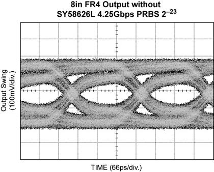
10 AC Electrical Characteristics (9) V CC = 3.3V ±10%; V EE = 0V; T A = 0 C to + 70 C; R L = 100Ω across output pair; unless otherwise stated. Symbol Parameter Condition Min Typ Max Units Freq Data Rate Throughput (TXQ) 1.5V PK output swing, No pre-emphasis 400mV output swing, 33% pre-emphasis DC 6.4 DC 6.4 Data Rate Throughput (TXLBQ) 400mV output swing DC 6.4 Gbps t pd Differential Propagation Delay TXIN-to-TXQ (V IN >200mV PK) ps RXLBIN-to-TXQ 250 ps t pd Tempco Differential Propagation Delay Temperature Coefficient 120 fs/ o C t EN TXQ Enable/Disable Time /TXEN 600 ps t LB_EN TXLBQ Enable/Disable Time /TXLBEN 200 ps t SHDN TXQ Shutdown Time /TXQ_SHDN HIGH-to-LOW (TXQ Outputs SHUTDOWN) /TXQ_SHDN LOW-to-HIGH (TXQ Outputs ON) ns t LBSEL Loopback Select Time LBSEL ps t PROG Programming Logic Control Time 3-bit pre-emphasis magnitude, 2-bit duration control 1 ns update-to-valid TXQ (0,0,0) 10 Pre-emphasis Magnitude (0,0,1) 15 MAG_CTRL (Percent beyond base swing) (0,1,0) 25 % MAG_CTRL (2,1,0) (0,1,1) 33 (1,X,X) 0 Minimum (shortest) 60 DUR_CTRL Pre-emphasis Duration Medium-short 100 DUR_CTRL (1,0) Medium-long 200 ps Longest 400 t SKEW Part-to-Part Skew Note ps t JITTER Random Jitter (RJ) Note 11, 13, 14, 15 1 ps Deterministic Jitter (DJ) Note 12, 13, 14, ps t r, t f Output Rise/Fall Time (20% to 80%) At full output swing ps Notes: 9. High-frequency AC-parameters are guaranteed by design and characterization. 10. Part-to-part skew is defined for two parts with identical power supply voltages at the same temperature and with no skew of the edges at the respective inputs. 11. This jitter is the RMS difference between the RJ measured at the end of a 9in FR4 transmission line driven by the SY58626 and the signal source. 12. This jitter is a difference between the DJ measured at the end of a 9in FR4 transmission path driven by an SY58626 and the signal source. 13. PE Mag: 010 and PE Dur: The typical jitter is measured at 4.25Gbps and 6.4Gbps using PRBS 2 7 pattern and 4.25Gbps using K28.5 pattern. 15. The transmission line is differential 6mil FR4 stripline with 100Ω differential impedance. Gbps June M C
11 Detailed Description The is a high speed, low jitter transmit buffer with integrated loopback capability. Adjustable pre-emphasis amplitudes and selectable pre-emphasis durations are included with the transmitter. The also includes disable and shutdown control for the transmitter output. Transmitter The transmitter includes the VTTIN and VTTOUT pin for maximum interface flexibility and DCoffset capability for the input and output, respectively. This feature allows for interfacing with different logic families without the use of AC-coupling. The output buffer has internal 50Ω source terminated CML outputs for minimizing round-trip reflections. Control of the transmitter output swing buffer can be obtained by using a variable resistor connected between VREF-CTRL and VCC with the wiper driving TXVCTRL. Please refer to Figure 1 for more details. Transmitter Disable and Shutdown The provides two methods to turn off the output when desired. When /TXEN is pulled HIGH, the transmitter output pair is disabled. TXQ goes to a LOW state and /TXQ goes to a HIGH state. When /TXQSHDN is pulled LOW, the transmitter output pair is in shutdown mode. TXQ and /TXQ output currents are shut off and the TXQ and /TXQ outputs are set to the same potential. The threshold for the /TXEN and /TXQSHDN pins is set with the VTH pin. Please refer to the Typical Operating Characteristics for more details. Loopback The features a loopback test mode, activated by setting LBSEL to logic HIGH. Using the with the SY58627L enables local loopback and link side loopback, shown in Figures 2b and 2c. This mode enables an external loopback path, bypassing circuitry on both local and link side. Please refer to Table 1 and Figure 3 for Loopback Control information. Figure 1. Variable Output Swing Circuit Transmitter Variable-Swing Output Buffer Connecting VREF-CTRL to TXVCTRL sets the transmitter output buffer to max swing 1.5V PK (3.0V PP ). Connecting VCC to TXVCTRL sets the transmitter output buffer to minimum swing 100mV PK (200mV PP ). Connecting VREF-FIXED to TXVCTRL sets the transmitter output buffer to 400mV PK (800mV PP ). Figure 2a. Normal Operation June M C
12 TXLB TXLBENb TXENb TXQ TXLBQ Normal Mode Link Side Loopback Mode TXIN TXIN TXIN TXIN RXLBIN TXIN TXIN RXLBIN Table 1. Transmit Loopback Control Signal Figure 2b. Local Loopback Mode Figure 3. Loopback Control Pin Figure 2c. Link Side Loopback Mode June M C


13 Typical Operating Characteristics V CC = 3.3V ±10%; V IN > 400mV; T A = 25 C, R L = 100Ω across output pair; unless otherwise stated. June M C
14 Typical Operating Characteristics (Continued) V CC = 3.3V ±10%; V IN > 400mV; T A = 25 C, R L = 100Ω across output pair; unless otherwise stated. Output Disable Output Shutdown TXQ /TXQ HIGH TXQ LOW /TXQ /TXEN HIGH LOW /TXQSHDN HIGH LOW Time (250ns/div.) Time (250ns/div.) June M C
15 Single-Ended and Differential Swings Figure 4a. Single-Ended Voltage Swing Figure 4b. Differential Voltage Swing Input and Output Stages Figure 5a. Simplified Differential Input Stage Figure 5b. Simplified Differential Output Stage June M C
16 Input Interface Applications Figure 6a. LVPECL Interface (DC-Coupled) Figure 6b. LVPECL Interface (AC-Coupled) option: may connect VTTIN to VCC Figure 6c. CML Interface (DC-Coupled) Figure 6d. CML Interface (AC-Coupled) Figure 6e. LVDS Interface (DC-Coupled) June M C
17 CML Output Interface Applications Figure 7a. CML DC-Coupled Termination Figure 7b. CML DC-Coupled Termination Figure 7c. CML AC-Coupled Termination Related Product and Support Information Part Number Function Datasheet Link SY58627L DC-to-6.4Gbps Backplane Receive Buffer with 4- Stage Programmable Equalization and DC-Offset Control HBW Solutions New Products and Applications June M C
18 Package Information Package Notes: 32-Pin QFN 1. Package meets Level 2 Moisture Sensitivity Classification. 2. All parts are dry-packed before shipment. 3. Exposed pad must be soldered to a ground for proper thermal management. MICREL, INC FORTUNE DRIVE SAN JOSE, CA USA TEL +1 (408) FAX +1 (408) WEB The information furnished by Micrel in this data sheet is believed to be accurate and reliable. However, no responsibility is assumed by Micrel for its use. Micrel reserves the right to change circuitry and specifications at any time without notification to the customer. Micrel Products are not designed or authorized for use as components in life support appliances, devices or systems where malfunction of a product can reasonably be expected to result in personal injury. Life support devices or systems are devices or systems that (a) are intended for surgical implant into the body or (b) support or sustain life, and whose failure to perform can be reasonably expected to result in a significant injury to the user. A Purchaser s use or sale of Micrel Products for use in life support appliances, devices or systems is a Purchaser s own risk and Purchaser agrees to fully indemnify Micrel for any damages resulting from such use or sale Micrel, Incorporated. June M C
Features. Applications. Markets
 Precision Low-Power Dual 2:1 LVPECL MUX with Internal Termination General Description The features two, low jitter 2:1 differential multiplexers with 100K LVPECL (800mV) compatible outputs, capable of
SY89847U. General Description. Functional Block Diagram. Applications. Markets
 1.5GHz Precision, LVDS 1:5 Fanout with 2:1 MUX and Fail Safe Input with Internal Termination General Description The is a 2.5V, 1:5 LVDS fanout buffer with a 2:1 differential input multiplexer (MUX). A
SY89854U. General Description. Features. Typical Applications. Applications
 Precision Low Power 1:4 LVPECL Fanout Buffer/Translator with Internal Termination General Description The is a 2.5V/3.3V precision, highspeed, fully differential 1:4 LVPECL fanout buffer. Optimized to
Features. Applications. Markets
 1.5GHz Precision, LVPECL 1:5 Fanout with 2:1 MUX and Fail Safe Input with Internal Termination Precision Edge General Description The is a 2.5/3.3V, 1:5 LVPECL fanout buffer with a 2:1 differential input
Features. Applications. Markets
 3.2Gbps Precision, LVDS 2:1 MUX with Internal Termination and Fail Safe Input General Description The is a 2.5V, high-speed, fully differential LVDS 2:1 MUX capable of processing clocks up to 2.5GHz and
ULTRA PRECISION 4 4 CML SWITCH WITH INTERNAL I/O TERMINATION
 ULTRA PRECISION 4 4 CML SWITCH WITH INTERNAL I/O TERMINATION Precision Edge FEATURES Provides crosspoint switching between any input pair to any output pair Ultra-low jitter design: 67fs RMS phase jitter
Features. Micrel Inc Fortune Drive San Jose, CA USA tel +1 (408) fax + 1 (408)
 fax + 1 (408)") 2.5V Low Jitter, Low Skew 1:12 LVDS Fanout Buffer with 2:1 Input MUX and Internal Termination General Description The is a 2.5V low jitter, low skew, 1:12 LVDS fanout buffer optimized for precision telecom
2.5V Low Jitter, Low Skew 1:12 LVDS Fanout Buffer with 2:1 Input MUX and Internal Termination General Description The is a 2.5V low jitter, low skew, 1:12 LVDS fanout buffer optimized for precision telecom
NOT RECOMMENDED FOR NEW DESIGNS. Features. Applications. Markets
 NOT RECOMMENDED FOR NEW DESIGNS Low Voltage 1.2V/1.8V/2.5V CML 2x2 Crosspoint Switch 6.4Gbps with Equalization General Description The is a fully-differential, low-voltage 1.2V/1.8V/2.5V CML 2x2 crosspoint
SY89850U. General Description. Features. Typical Application. Applications. Markets
 Precision Low-Power LVPECL Line Driver/Receiver with Internal Termination General Description The is a 2.5V/3.3V precision, high-speed, differential receiver capable of handling clocks up to 4GHz and data
ULTRA PRECISION 8:1 MUX WITH INTERNAL TERMINATION AND 1:2 400mV LVPECL FANOUT BUFFER
 ULTRA PRECISION 8:1 MUX WITH INTERNAL TERMINATION AND 1:2 400mV LVPECL FANOUT BUFFER FEATURES Selects between 1 of 8 inputs, and provides 2 precision, low skew LVPECL output copies Guaranteed AC performance
ULTRA PRECISION 4 4 CML SWITCH WITH INTERNAL I/O TERMINATION
 ULTRA PRECISION 4 4 CML SWITCH WITH INTERNAL I/O TERMINATION Precision Edge FEATURES Provides crosspoint switching between any input pair to any output pair Guaranteed AC performance over temperature and
Features. Applications. Markets
 Low Voltage 1.2V/1.8V/2.5V CML 1:4 Fanout Buffer with /EN 3.2Gbps, 3.2GHz General Description The is a fully differential, low voltage 1.2V/1.8V/2.5V CML 1:4 Fanout Buffer with active-low Enable (/EN).
ULTRA PRECISION 8:1 MUX WITH INTERNAL TERMINATION AND 1:2 CML FANOUT BUFFER
 , IIIIInc. ULTRA PRECISION 8:1 MUX WITH TERNAL TERMATION AND 1:2 CML FANOUT BUFFER Precision Edge Precision Edge FEATURES Selects between 1 of 8 inputs, and provides two precision, low skew CML output
ULTRA PRECISION DIFFERENTIAL CML 4:1 MUX WITH 1:2 FANOUT AND INTERNAL I/O TERMINATION
 ULTRA PRECISION DIFFERENTIAL CML 4:1 MUX WITH 1:2 FANOUT AND TERNAL I/O TERMATION FEATURES Selects 1 of 4 differential inputs Provides two copies of the selected input Guaranteed AC performance over temperature
Features. Applications. Markets
 1GHz Precision, LVDS 3, 5 Clock Divider with Fail Safe Input and Internal Termination General Description The is a precision, low jitter 1GHz 3, 5 clock divider with an LVDS output. A unique Fail- Safe
Features. Applications. Markets
 Precision LVPECL Runt Pulse Eliminator 2:1 MUX with 1:2 Fanout and Internal Termination General Description The is a low jitter PECL, 2:1 differential input multiplexer (MUX) optimized for redundant source
Features. Applications. Markets
 Precision LVPECL Runt Pulse Eliminator 2:1 Multiplexer General Description The is a low jitter PECL, 2:1 differential input multiplexer (MUX) optimized for redundant source switchover applications. Unlike
6GHz, 1:6 CML FANOUT BUFFER WITH 2:1 MUX INPUT AND INTERNAL I/O TERMINATION
 6GHz, 1:6 CML FANOUT BUFFER WITH 2:1 MUX PUT AND TERNAL I/O TERMATION Precision Edge FEATURES Provides six ultra-low skew copies of the selected input 2:1 MUX input included for clock switchover applications
PRECISION 1:8 LVPECL FANOUT BUFFER WITH 2:1 RUNT PULSE ELIMINATOR INPUT MUX
 PRECISION 1:8 LVPECL FANOUT BUFFER WITH 2:1 RUNT PULSE ELIMINATOR INPUT MUX FEATURES Selects between two clocks, and provides 8 precision, low skew LVPECL output copies Guaranteed AC performance over temperature
ULTRA-PRECISION DIFFERENTIAL CML 2:1 MUX with INTERNAL I/O TERMINATION
 ULTRA-PRECISION DIFFERENTIAL CML 2:1 MUX with TERNAL I/O TERMATION FEATURES Guaranteed AC performance over temperature and voltage: DC to > 10.7Gbps data throughput DC to > 7GHz f MAX (clock) < 240ps propagation
SY89841U. General Description. Features. Applications. Markets. Precision LVDS Runt Pulse Eliminator 2:1 Multiplexer
 SY89841U Precision LVDS Runt Pulse Eliminator 2:1 Multiplexer General Description The SY89841U is a low jitter LVDS, 2:1 input multiplexer (MUX) optimized for redundant source switchover applications.
ULTRA-PRECISION DIFFERENTIAL LVPECL 2:1 MUX with INTERNAL TERMINATION
 ULTRA-PRECISION DIFFERENTIAL LVPECL 2:1 MUX with TERNAL TERMATION FEATURES Guaranteed AC performance over temperature and voltage: DC to 5Gbps data throughput DC to > 4GHz f MAX (clock) < 260ps propagation
SY89838U. General Description. Features. Applications. Markets. Precision 1:8 LVDS Clock Fanout Buffer with 2:1 Runt Pulse Eliminator Input MUX
 Precision 1:8 LVDS Clock Fanout Buffer with 2:1 Runt Pulse Eliminator Input MUX General Description The is a low jitter, low skew, high-speed 1:8 fanout buffer with a unique, 2:1 differential input multiplexer
SY89540U. General Description. Features. Typical Performance. Applications. Precision Low Jitter 4x4 LVDS Crosspoint Switch with Internal Termination
 Precision Low Jitter 4x4 LVDS Crosspoint Switch with Internal Termination General Description The is a low-jitter, low skew, high-speed 4x4 crosspoint switch optimized for precision telecom and enterprise
NOT RECOMMENDED FOR NEW DESIGNS
 NOT RECOMMENDED FOR NEW DESIGNS ULTRA PRECISION 8:1 MUX WITH INTERNAL TERMINATION AND 1:2 400mV LVPECL FANOUT BUFFER FEATURES - Selects between 1 of 8 inputs, and provides 2 precision, low skew LVPECL
Features. Applications. Markets
 3.2Gbps Precision, 1:2 LVPECL Fanout Buffer with Internal Termination and Fail Safe Input General Description The is a 2.5/3.3V, high-speed, fully differential 1:2 LVPECL fanout buffer optimized to provide
SY89540U. General Description. Features. Typical Performance. Applications. Precision Low Jitter 4x4 LVDS Crosspoint Switch with Internal Termination
 Precision Low Jitter 4x4 LVDS Crosspoint Switch with Internal Termination General Description The is a low-jitter, low skew, high-speed 4x4 crosspoint switch optimized for precision telecom and enterprise
SY58608U. General Description. Features. Functional Block Diagram
 3.2Gbps Precision, 1:2 LVDS Fanout Buffer with Internal Termination and Fail Safe Input General Description The is a 2.5V, high-speed, fully differential 1:2 LVDS fanout buffer optimized to provide two
Features. Applications. Markets
 2GHz, Low-Power, 1:6 LVPECL Fanout Buffer with 2:1 Input MUX and Internal Termination General Description The is a 2.5V/3.3V precision, high-speed, 1:6 fanout capable of handling clocks up to 2.0GHz. A
AND INTERNAL TERMINATION
 4.5GHz, 1:6 LVPECL Fanout Buffer WITH 2:1 MUX Input AND TERNAL TERMATION FEATURES Provides six ultra-low skew copies of the selected input 2:1 MUX input included for clock switchover applications Guaranteed
Features. Applications. Markets
 Low oltage 1.2/1.8 CML 2:1 MUX 3.2Gbps, 2.5GHz General Description The is a fully differential, low voltage 1.2/1.8 CML 2:1 MUX. The can process clock signals as fast as 3.2GHz or data patterns up to 3.2Gbps.
SY56216R. General Description. Features. Applications. Functional Block Diagram. Markets
 Low Voltage 1.2V/1.8V/2.5V CML Dual Channel Buffer 4.5GHz/6.4Gbps with Equalization General Description The is a fully-differential, low-voltage 1.2V/1.8V/2.5V CML Dual Channel Buffer with input equalization.
ULTRA PRECISION DIFFERENTIAL LVPECL 4:1 MUX with 1:2 FANOUT and INTERNAL TERMINATION
 ULTRA PRECISION DIFFERENTIAL LVPECL 4:1 MUX with 1:2 FANOUT and TERNAL TERMATION FEATURES Selects 1 of 4 differential inputs Provides two copies of the selected input Guaranteed AC performance over temperature
Features. Applications. Markets
 4.25Gbps Precision, 1:2 CML Fanout Buffer with Internal Termination and Fail Safe Input General Description The is a 2.5/3.3V, high-speed, fully differential 1:2 CML fanout buffer optimized to provide
Features. Applications
 Ultra-Precision, 8:1 MUX with Internal Termination and 1:2 LVPECL Fanout Buffer Precision Edge General Description The is a low-jitter, low-skew, high-speed 8:1 multiplexer with a 1:2 differential fanout
Features. Applications
 Ultra-Precision 1:8 LVDS Fanout Buffer with Three 1/ 2/ 4 Clock Divider Output Banks Revision 6.0 General Description The is a 2.5V precision, high-speed, integrated clock divider and LVDS fanout buffer
Features. Applications
 Ultra-Precision CML Data and Clock Synchronizer with Internal Input and Output Termination Precision Edge General Description The is an ultra-fast, precision, low jitter datato-clock resynchronizer with
ULTRA-PRECISION DIFFERENTIAL CML LINE DRIVER/RECEIVER WITH INTERNAL TERMINATION
 ULTRA-PRECISION DIFFERENTIAL CML LE DRIVER/RECEIVER WITH TERNAL TERMATION FEATURES Guaranteed AC performance over temperature and voltage: DC-to >10.7Gbps data rate throughput DC-to >7GHz clock f MAX
ULTRA PRECISION DUAL 2:1 LVPECL MUX WITH INTERNAL TERMINATION
 ULTRA PRECISION DUAL 2:1 LVPECL MUX WITH TERNAL TERMATION FEATURES Two independent differential 2:1 multiplexers Guaranteed AC performance over temperature and voltage: DC-to >5Gbps data rate throughput
Features. Applications. Markets
 3.2Gbps Precision, LVPECL Buffer with Internal Termination and Fail Safe Input General Description The is a 2.5/3.3V, high-speed, fully differential LVPECL buffer optimized to provide only 108fs RMS phase
ULTRA-PRECISION DIFFERENTIAL 800mV LVPECL LINE DRIVER/RECEIVER WITH INTERNAL TERMINATION
 ULTRA-PRECISION DIFFERENTIAL 800mV LVPECL LE DRIVER/RECEIVER WITH TERNAL TERMATION FEATURES Guaranteed AC performance over temperature and voltage: DC-to >5Gbps data rate throughput DC-to >5GHz clock f
Features. Applications
 2.5GHz, Any Differential, In-to-LVPECL, Programmable Clock Divider/Fanout Buffer with Internal Termination General Description This low-skew, low-jitter device is capable of accepting a high-speed (e.g.,
Precision Edge SY89876L DESCRIPTION FEATURES TYPICAL PERFORMANCE APPLICATIONS FUNCTIONAL BLOCK DIAGRAM
 3.3V, 2.0GHz ANY DIFFERENTIAL -TO-LVDS PROGRAMMABLE CLOCK DIVIDER AND 1:2 FANOUT BUFFER W/ TERNAL TERMATION FEATURES DESCRIPTION Integrated programmable clock divider and 1:2 fanout buffer Guaranteed AC
Features. Applications. Markets
 Low Voltage 1.2V/1.8V CML Differential Line Driver/Receiver 3.2Gbps, 3.2GHz General Description The is a fully-differential, low-voltage 1.2V/1.8V CML Line Driver/Receiver. The can process clock signals
5GHz, 1:2 LVPECL FANOUT BUFFER/TRANSLATOR WITH INTERNAL INPUT TERMINATION
 5GHz, 1:2 LVPECL FANOUT BUFFER/TRANSLATOR WITH TERNAL PUT TERMATION FEATURES Precision 1:2, 800mV LVPECL fanout buffer Guaranteed AC performance over temperature/ voltage: > 5GHz f MAX (clock) < 110ps
7GHz, 1:2 CML FANOUT BUFFER/TRANSLATOR WITH INTERNAL I/O TERMINATION
 7GHz, 1:2 CML FANOUT BUFFER/TRANSLATOR WITH TERNAL I/O TERMATION Precision Edge FEATURES - Precision 1:2, 400mV CML fanout buffer - Low jitter performance: 49fs RMS phase jitter (typ) - Guaranteed AC performance
SY89871U. General Description. Features. Typical Performance. Applications
 2.5GHz Any Diff. In-To-LVPECL Programmable Clock Divider/Fanout Buffer w/ Internal Termination General Description The is a 2.5V/3.3V LVPECL output precision clock divider capable of accepting a high-speed
4GHz, 1:4 LVPECL FANOUT BUFFER/ TRANSLATOR WITH INTERNAL TERMINATION
 4GHz, 1:4 LVPECL FANOUT BUFFER/ TRANSLATOR WITH TERNAL TERMATION FEATURES Precision 1:4, LVPECL fanout buffer Guaranteed AC performance over temperature/ voltage: >4GHz f MAX (clock)
3.3V/5V 800MHz LVTTL/LVCMOS-to-DIFFERENTIAL LVPECL TRANSLATOR
 3.3V/5V 800MHz LVTTL/LVCMOS-to-DIFFERENTIAL LVPECL TRANSLATOR FEATURES Guaranteed AC performance over temp and voltage: DC-to-800MHz f MAX
5.5GHz 1:4 FANOUT BUFFER/ TRANSLATOR w/400mv LVPECL OUTPUTS AND INTERNAL INPUT TERMINATION. Precision Edge SY58022U FEATURES DESCRIPTION APPLICATIONS
 5.5GHz 1:4 FANOUT BUFFER/ TRANSLATOR w/400mv LVPECL OUTPUTS AND TERNAL PUT TERMATION FEATURES Precision 1:4, 400mV LVPECL fanout buffer Guaranteed AC performance over temperature and voltage: > 5.5GHz
SY89297U. General Description. Features. Applications. Markets. 2.5/3.3V, 3.2Gbps Precision CML Dual-Channel Programmable Delay
 2.5/3.3V, 3.2Gbps Precision CML Dual-Channel Programmable Delay General Description The is a DC-3.2Gbps programmable, twochannel delay line. Each channel has a delay range from 2ns to 7ns (5ns delta delay)
NOT RECOMMENDED FOR NEW DESIGNS. 3.3V/5V 3GHz PECL/ECL 2:1 MULTIPLEXER
 NOT RECOMMENDED FOR NEW DESIGNS Micrel, Inc. 3.3V/5V 3GHz PECL/ECL 2:1 MULTIPLEXER FEATURES 2:1 PECL/ECL multiplexer Guaranteed AC-performance over temperature/ voltage >3GHz f MAX (toggle)
3.3V/5V PECL/ECL 3GHz DUAL DIFFERENTIAL 2:1 MULTIPLEXER
 3.3V/5V PECL/ECL 3GHz DUAL DIFFERENTIAL 2:1 MULTIPLEXER FEATURES Dual, fully differential 2:1 PECL/ECL multiplexer Guaranteed AC parameters over temperature/ voltage: > 3GHz f MAX (toggle) < 100ps within
3.3V DIFFERENTIAL LVPECL/CML/LVDS-to-LVTTL TRANSLATOR
 3.3V DIFFERENTIAL LVPECL/CML/LVDS-to-LVTTL TRANSLATOR FEATURES 3.3V power supply 1.9ns typical propagation delay 275MHz f MAX Differential LVPECL/CML/LVDS inputs 24mA LVTTL outputs Flow-through pinouts
SY55859L. General Description. Features. Applications. 3.3V, 3.2Gbps Dual 2X2 Crosspoint Switch
 3.3V, 3.2Gbps Dual 2X2 Crosspoint Switch General Description The is a dual CML 2x2 crosspoint switch optimized for high-speed data and/or clock applications (up to 3.2Gbps or 2.7GHz) where low jitter and
3.3V/5V 2.5GHz PECL/ECL 1:4 FANOUT BUFFER WITH 2:1 INPUT MUX
 3.3V/5V 2.5GHz PECL/ECL 1:4 FANOUT BUFFER WITH 2:1 INPUT MUX FEATURES High-speed 1:4 PECL/ECL fanout buffer 2:1 multiplexer input Guaranteed AC parameters over temp/voltage: > 2.5GHz f MAX (toggle) < 225ps
Features. Truth Table (1)
") 3.3V/5V, 4GHz PECL/ECL 2 Clock Generator Precision Edge General Description The is an integrated 2 divider with differential clock inputs. It is functionally equivalent to the SY100EP32V but in an ultra-small
3.3V/5V, 4GHz PECL/ECL 2 Clock Generator Precision Edge General Description The is an integrated 2 divider with differential clock inputs. It is functionally equivalent to the SY100EP32V but in an ultra-small
SY88422L. General Description. Features. Applications. Typical Application. 4.25Gbps Laser Driver with Integrated Bias
 4.25Gbps Laser Driver with Integrated Bias General Description The is a single 3.3V supply, small form factor laser driver for telecom/datacom applications up to 4.25Gbps. The driver can deliver modulation
SY84403BL. General Description. Features. Applications. Typical Performance. Markets
 Ultra Small 3.3V 4.25Gbps CML Low-Power Limiting Post Amplifier with TTL LOS General Description The is the industry s smallest limiting post amplifier ideal for compact copper and fiber optic module applications.
5V/3.3V 2.5Gbps LASER DIODE DRIVER
 5V/3.3V 2.5Gbps LASER DIODE DRIVER FEATURES DESCRIPTION Up to 2.5Gbps operation 30mA modulation current Separate modulation control Separate output enable for laser safety Differential inputs for data
SY58016L. Features. General Description. Applications. Package/Ordering Information. Pin Description
 3.3V, 10Gbps Differential CML Line Driver/Receiver with Internal Termination General Description The is a high-speed, current mode logic (CML) differential receiver. It is ideal for interfacing with high
Features. Applications
 PCIe Fanout Buffer 267MHz, 8 HCSL Outputs with 2 Input MUX PrecisionEdge General Description The is a high-speed, fully differential 1:8 clock fanout buffer optimized to provide eight identical output
3.3V/5V DUAL LVTTL/LVCMOS-to-DIFFERENTIAL LVPECL TRANSLATOR
 3.3V/5V DUAL LVTTL/LVCMOS-to-DIFFERENTIAL LVPECL TRANSLATOR Precision Edge FEATURES 3.3V and 5V power supply option 300ps typical propagation delay Differential LVPECL outputs PNP LVTTL inputs for minimal
SY88992L. Features. General Description. Applications. Markets. Typical Application. 3.3V, 4.25Gbps VCSEL Driver
 3.3V, 4.25Gbps VCSEL Driver General Description The is a single supply 3.3V, low power consumption, small-form factor VCSEL driver ideal for use in datacom applications; Ethernet, GbE (Gigabit Ethernet),
Features. Applications. Markets
 3.3V, 3.2Gbps PECL Limiting Post Amplifier with Wide Signal-Detect Range General Description The low-power limiting post amplifiers are designed for use in fiber-optic receivers. These devices connect
3.3V/5V 3GHz PECL/ECL 2:1 MULTIPLEXER
 3.3V/5V 3GHz PECL/ECL 2:1 MULTIPLEXER FEATURES 2:1 PECL/ECL multiplexer Guaranteed AC performance over temperature/voltage >3GHz f MAX (toggle)
2.5/3.3V 1:22 HIGH-PERFORMANCE, LOW-VOLTAGE PECL BUS CLOCK DRIVER & TRANSLATOR w/ INTERNAL TERMINATION
 2.5/3.3V 1:22 HIGH-PERFORMANCE, LOW-VOLTAGE PECL BUS CLOCK DRIVER & TRANSLATOR w/ INTERNAL TERMINATION FEATURES LVPECL or LVDS input to 22 LVPECL outputs 100K ECL compatible outputs LVDS input includes
SY88149HL. Features. General Description. Applications. Markets. 3.3V 1.25Gbps Burst-Mode Limiting Amplifier with Ultra-Fast Signal Assert Timing
 3.3V 1.25Gbps Burst-Mode Limiting Amplifier with Ultra-Fast Signal Assert Timing General Description The is a high-sensitivity, burst-mode capable limiting post amplifier designed for Optical Line Terminal
3.3V, 1.5GHz 1/ 2 DIFFERENTIAL LVECL/LVPECL PROGRAMMABLE CLOCK GENERATOR AND 1:15 FANOUT BUFFER
 3.3V, 1.5GHz 1/ 2 DIFFERENTIAL LVECL/LVPECL PROGRAMMABLE CLOCK GENERATOR AND 1:15 FANOUT BUFFER FEATURES Four programmable output banks and 15 total LVPECL-compatible differential outputs Pin-compatible,
NOT RECOMMENDED FOR NEW DESIGNS
 NOT RECOMMENDED FOR NEW DESIGNS 2.5V/3.3V 2.5GHz DIFFERENTIAL 2-CHANNEL PRECISION CML DELAY LINE FEATURES Guaranteed AC parameters over temp and voltage > 2.5GHz f MAX < 384ps prop delay < 120ps t r /t
D LATCH. SuperLite SY55853U FEATURES DESCRIPTION FUNCTIONAL BLOCK DIAGRAM APPLICATIONS
 D LATCH FEATURES 2.5GHz min f max 2.3V to 5.7V power supply Single bit latch Stores or flows through 1 bit of data Optimized to work with family Fully differential Source terminated CML outputs for fast
SY58051U. General Description. Features. Typical Application. Applications
 SY58051U Ultra-Precision CM AnyGate with Internal Input and Output Termination Precision Edge General Description The SY58051U is an ultra-fast, low jitter universal logic gate with a guaranteed maximum
5V/3.3V 622Mbps LASER DIODE DRIVER WITH OUTPUT ENABLE
 5V/3.3V 622Mbps LASER DIODE DRIVER WITH OUTPUT ENABLE FEATURES DESCRIPTION Single 3.3V or 5V power supply Up to 622Mbps operation Modulation current to 30mA PECL output enable Differential PECL inputs
SY88982L. Features. General Description. Applications. Markets. Typical Application
 3.3V, 2.7Gbps High-Current, Low-Power Laser Driver for FP/DFB Lasers General Description The is a single 3.3V supply, low power consumption, small form factor driver for telecom/datacom applications using
5V/3.3V 155Mbps LASER DIODE DRIVER WITH OUTPUT ENABLE
 5V/3.3V 155Mbps LASER DIODE DRIVER WITH OUTPUT ENABLE FEATURES DESCRIPTION Single 3.3V or 5V power supply Up to 155Mbps operation Modulation current to 30mA PECL output enable Differential PECL inputs
Features. Applications
 267MHz 1:2 3.3V HCSL/LVDS Fanout Buffer PrecisionEdge General Description The is a high-speed, fully differential 1:2 clock fanout buffer with a 2:1 input MUX optimized to provide two identical output
SY88149HAL. Features. General Description. Applications. Markets. 1.25Gbps Burst-Mode Limiting Amplifier with Ultra-Fast Signal Assert Timing
 1.25Gbps Burst-Mode Limiting Amplifier with Ultra-Fast Signal Assert Timing General Description The is a high-sensitivity, burst-mode capable, limiting-post amplifier designed for FTTH PON optical line
5V/3.3V 4-INPUT OR/NOR
 5V/3.3V 4-INPUT OR/NOR FEATURES 3.3V and 5V power supply options 230ps typical propagation delay High bandwidth to 3GHz 75kΩ internal input pulldown resistors Q output will default LOW with inputs open
D FLIP-FLOP. SuperLite SY55852U FEATURES DESCRIPTION FUNCTIONAL BLOCK DIAGRAM APPLICATIONS
 D FLIP-FLOP FEATURES 2.5GHz min. f MAX 2.3V to 5.7V power supply Single bit register memory Synchronizes 1 bit of data to a clock Optimized to work with family Fully differential Accepts CML, PECL, LVPECL
SY88993AL. Features. General Description. Applications. Markets. 3.3V 3.2Gbps High-Speed Limiting Post Amplifier with High Input Sensitivity
 3.3V 3.2Gbps High-Speed Limiting Post Amplifier with High Input Sensitivity General Description The limiting post amplifier, with its wide bandwidth, is ideal for use as a post amplifier in fiber-optic
5V 155Mbps LASER DIODE DRIVER WITH OUTPUT ENABLE
 V 1Mbps LASER DIODE DRIVER WITH OUTPUT ENABLE FEATURES DESCRIPTION Up to 1Mbps operation Modulation current to 2mA PECL output enable Differential PECL inputs Single V power supply Available in a tiny
5V/3.3V, 3GHz PECL/LVPECL D FLIP-FLOP WITH SET AND RESET
 5V/3.3V, 3GHz PECL/LVPECL D FLIP-FLOP WITH SET AND RESET FEATURES Guaranteed >3GHz bandwidth over temperature Guaranteed
5V/3.3V DUAL DIFFERENTIAL 2:1 MULTIPLEXER
 5V/3.3V DUAL DIFFERENTIAL 2:1 MULTIPLEXER FEATURES DESCRIPTION 3.3V and 5V power supply options 440ps propagation delay Separate and common select High bandwidth output transitions Internal 75KΩ input
SY88236L/AL. General Description. Features. Applications. Typical Application. 2.5Gbps Burst Mode Laser Driver with Integrated Limiting Amplifier
 2.5Gbps Burst Mode Laser Driver with Integrated Limiting Amplifier General Description Features The SY88236L is a single supply 3.3V integrated burst mode laser driver and post amplifier for A-PON, B-PON,
5V/3.3V QUAD DIFFERENTIAL RECEIVER
 5V/3.3V QUAD DIFFERENTIAL RECEIVER FEATURES DESCRIPTION 3.3V and 5V power supply options High bandwidth output transitions Internal 75KΩ input pull down resistors Available in 20-pin SOIC package The is
NOT RECOMMENDED FOR NEW DESIGNS 5V/3.3V DIFFERENTIAL DATA AND CLOCK D FLIP-FLOP
 NOT RECOMMENDED FOR NEW DESIGNS Micrel, Inc. 5V/3.3V DIFFERENTIAL DATA AND CLOCK D FLIP-FLOP FEATURES Guaranteed maximum frequency >4GHz Guaranteed
SY88903AL. General Description. Features. Applications. Markets
 3.3V, Burst Mode 1.25Gbps PECL High- Sensitivity Limiting Post Amplifier with TTL Loss-of-Signal General Description The, burst mode, high-sensitivity limiting post amplifier is designed for use in fiber-optic
5V/3.3V DIFFERENTIAL 2-INPUT XOR/XNOR
 5V/3.3V DIFFERENTIAL 2-INPUT XOR/XNOR FEATURES 3.3V or 5V power supply options Maximum frequency > 3GHz typical 200ps typical propagation delay Internal input resistors: pulldown on D, pulldown and pullup
SY88953L. 3.3V 10.7Gbps CML LIMITING POST AMPLIFIER W/ TTL SD AND /SD SY88953L DESCRIPTION FEATURES APPLICATIONS TYPICAL APPLICATIONS CIRCUIT
 3.3V 10.7Gbps CML LIMITING POST AMPLIFIER W/ TTL SD AND /SD FEATURES DESCRIPTION Single 3.3V power supply Up to 10.7Gbps operation 800mVp-p output swing with 30ps edge rates 28dB voltage gain with 5mVp-p
5V/3.3V D FLIP-FLOP WITH RESET AND DIFFERENTIAL CLOCK
 5V/3.3V D FLIP-FLOP WITH RESET AND DIFFERENTIAL CLOCK FEATURES 3.3V and 5V power supply options 320ps typical propagation delay Maximum frequency > 3GHz typical 75KΩ internal input pulldown resistor Transistor
SM General Description. ClockWorks. Features. Applications. Block Diagram
 ClockWorks PCI-e Octal 100MHz/200MHz Ultra-Low Jitter, HCSL Frequency Synthesizer General Description The is a member of the ClockWorks family of devices from Micrel and provides an extremely low-noise
SM Features. General Description. Applications. Block Diagram. ClockWorks GbE (125MHz) Ultra-Low Jitter, LVPECL Frequency Synthesizer
 Ultra-Low Jitter, LVPECL Frequency Synthesizer") ClockWorks GbE (125MHz) Ultra-Low Jitter, LVPECL Frequency Synthesizer General Description The is a member of the ClockWorks family of devices from Micrel and provides an extremely low-noise timing solution
ClockWorks GbE (125MHz) Ultra-Low Jitter, LVPECL Frequency Synthesizer General Description The is a member of the ClockWorks family of devices from Micrel and provides an extremely low-noise timing solution
SM Features. General Description. Applications. Block Diagram
 ClockWorks 10GbE (156.25MHz, 312.5MHz), Ultra-Low Jitter, LVPECL Frequency Synthesizer General Description The is a member of the ClockWorks family of devices from Micrel and provides an extremely low-noise
5V/3.3V DIFFERENTIAL RECEIVER
 MicreL, Inc. 5V/3.3V DIFFERENTIAL RECEIVER FEATURES DESCRIPTION 3.3V and 5V power supply options 250ps propagation delay High bandwidth output transitions Internal 75KΩ input pull-down resistors Replaces
Features. Applications. Micrel Inc Fortune Drive San Jose, CA USA tel +1 (408) fax + 1 (408)
 fax + 1 (408)") Flexible Ultra-Low Jitter Clock Synthesizer Clockworks FLEX General Description The SM802xxx series is a member of the ClockWorks family of devices from Micrel and provide an extremely low-noise timing
Flexible Ultra-Low Jitter Clock Synthesizer Clockworks FLEX General Description The SM802xxx series is a member of the ClockWorks family of devices from Micrel and provide an extremely low-noise timing
NOT RECOMMENDED FOR NEW DESIGNS
 NOT RECOMMENDED FOR NEW DESIGNS 3.3V, DUAL DIFFERENTIAL LVPECL-TO-LVTTL TRANSLATOR FEATURES 3.3V power supply 2.0ns typical propagation delay
SM Features. General Description. Applications. Block Diagram. ClockWorks PCI-e Quad 100MHz Ultra-Low Jitter, HCSL Frequency Synthesizer
 ClockWorks PCI-e Quad 100MHz Ultra-Low Jitter, HCSL Frequency Synthesizer General Description The is a member of the ClockWorks family of devices from Micrel and provides an extremely low-noise timing
NOT RECOMMENDED FOR NEW DESIGNS 4:1 DIFFERENTIAL MULTIPLEXER
 NOT RECOMMENDED FOR NEW DESIGNS Micrel, Inc. 4:1 DIFFERENTIAL MULTIPLEXER FEATURES DESCRIPTION 5V power supply Useful as either 4:1 or 2:1 multiplexer VBB output for single-ended operation 75KΩ internal
Features. Applications. Micrel Inc Fortune Drive San Jose, CA USA tel +1 (408) fax + 1 (408)
 fax + 1 (408)") 3.3V 10.7Gbps CML Limiting Post Amplifier with TTL SD and /SD General Description The high-speed, limiting post amplifier is designed for use in fiber-optic receivers. The device connects to typical transimpedance
3.3V 10.7Gbps CML Limiting Post Amplifier with TTL SD and /SD General Description The high-speed, limiting post amplifier is designed for use in fiber-optic receivers. The device connects to typical transimpedance
3.3V/5V 2.5GHz PROGRAMMABLE DELAY
 3.3V/5V 2.5GHz PROGRAMMABLE DELAY FEATURES Pin-for-pin, plug-in compatible to the ON Semiconductor MCEP95 Maximum frequency > 2.5GHz Programmable range: 2.2ns to 2.2ns ps increments PECL mode operating