SY88993AL. Features. General Description. Applications. Markets. 3.3V 3.2Gbps High-Speed Limiting Post Amplifier with High Input Sensitivity
|
|
|
- Osborn Roberts
- 5 years ago
- Views:
Transcription
1 3.3V 3.2Gbps High-Speed Limiting Post Amplifier with High Input Sensitivity General Description The limiting post amplifier, with its wide bandwidth, is ideal for use as a post amplifier in fiber-optic receivers with data rates up to 3.2Gbps. Signals as small as 4mV PP can be amplified to drive devices with CML inputs or AC-coupled PECL inputs. The generates a chatter-free Loss-of-Signal (LOS) open collector TTL output using an external resistor, as shown Figure 1. The incorporates a programmable level detect function to identify when the input signal has been lost. This information can be fed back to the /EN input of the device to maintain stability under loss of signal conditions. Using LOS LVL pin the sensitivity of the level detect can be adjusted. The LOS LVL voltage can be set by connecting a resistor divider between V CC and V REF, Figure 5. Datasheets and support documentation can be found on Micrel s web site at: Features Up to 3.2Gbps operation Low noise CML data outputs Chatter-Free LOS generation Open Collector TTL LOS output TTL /EN Input Differential PECL inputs for data Single 3.3V power supply Available in a tiny 10-pin (3mm x 3mm) MSOP Applications PON SFP/SFF/GBIC optical transceivers Gigabit Ethernet 1X and 2X Fibre Channel SONET/SDH: OC 3/12/24/48 STM 1/4/8/16 Line driver and line receiver Markets FTTX Datacom/Telecom Figure 1. LOS LVL resistor configuration Micrel Inc Fortune Drive San Jose, CA USA tel +1 (408) fax + 1 (408) September 2008 M A
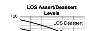
2 Block Diagram Detailed Description The is a high-sensitivity limiting post amplifier that operates from a single +3.3V power supply, over temperatures from 40 o C to +85 o C. Signals with data rates up to 3.2Gbps and as small as 4mV PP can be amplified. Figure 2 shows the allowed input voltage swing. The generates a LOS output. LOS LVL sets the sensitivity of the input amplitude detection. Input Amplifier/Buffer Figure 3 shows a simplified schematic of the s input stage. The high-sensitivity of the input amplifier allows signals as small as 4mV PP to be detected and amplified. The input amplifier also allows input signals as large as 1800mV PP. Input signals below 6mVpp are linearly amplified with a typical 38dB differential voltage gain. Since it is a limiting amplifier, the outputs typically 800mV PP voltagelimited waveforms for input signals that are greater than 10mV PP. Applications requiring the to operate with high-gain should have the upstream TIA placed as close as possible to the s input pins to ensure the best performance of the device. Output Buffer The s CML output buffer is designed to drive 50Ω lines. The output buffer requires appropriate termination for proper operation. An external 50Ω resistor to V CC for each output pin provides this. Figure 4 shows a simplified schematic of the output stage. Loss-of-Signal The generates a chatter-free LOS opencollector TTL output which requires an external pull-up resistor, as shown in Figure 1. LOS is used to determine that the input amplitude is large enough to be considered a valid input. LOS asserts high if the input amplitude falls below the threshold sets by LOS LVL and de-asserts low otherwise. LOS can be fed back to the enable bar (/EN) input to maintain output stability under a loss of signal condition. /EN de-asserts the true output signal without removing the input signals. Typically, 5.6dB LOS hysteresis is provided to prevent chattering. Loss-of-Signal Level Set The incorporates a programmable level detect function to identify when the input signal has been lost. This information can be fed back to the /EN input of the device to maintain stability under loss of signal conditions. Using LOS LVL pin the sensitivity of the level detect can be adjusted. The LOS LVL voltage can be set by connection a resistor divider between V CC and V REF, Figure 5. Hysteresis The typically provides 5.6dB LOS electrical hysteresis. By definition, a power ratio measured in db is 10log (power ratio). Power is calculated as V 2 IN/R for an electrical signal. Hence, the same ratio can be stated as 20log (voltage ratio). While in linear mode, the electrical voltage input changes linearly with the optical power and therefore, the ratios change linearly. Thus, the optical hysteresis in db is half the electrical hysteresis in db given in the data sheet. Since the is an electrical device, this data sheet refers to hysteresis in electrical terms. With 5.6dB LOS hysteresis, a voltage factor of about 2 is required to assert or de-assert LOS. September M A
3 Ordering Information Part Number Package Type Operating Range Package Marking KG K10-1 Industrial 993L with Pb-Free bar-line indicator KGTR (1) K10-1 Industrial 993L with Pb-Free bar-line indicator Note: 1. Tape and reel. Lead Finish Pb-Free NiPdAu Pb-Free NiPdAu Pin Configuration 10-Pin MSOP (K10-1) Pin Description Pin Number Pin Name Pin Function 1 /EN TTL (Input): Output enable (Active Low). 2 DIN Data (Input): Data input. 3 /DIN Data (Input): Complementary data input. 4 VREF Output: Reference voltage output for LOS Level Set (See Figure 3). 5 LOSLVL Input: Loss-of-Signal Level Set 6 GND Ground. 7 LOS TTL Output (Open Collector): Loss-of-Signal indicator (Active High). 8 /DOUT CML (Output): Inverting data output. 9 DOUT CML (Output): Data output. 10 VCC Power Supply: Positive power supply. September M A
4 Absolute Maximum Ratings (1) Supply Voltage (V CC )... 0V to +4.0V Input Voltage (DIN, /DIN)... 0V to V CC Lead Temperature (soldering, #sec.) C Storage Temperature (T s ) C to +85 C Operating Ratings (2) Supply Voltage (V IN ) V to +3.6V Ambient Temperature (T A ) C to +85 C Junction Thermal Resistance MSOP (θ JA ) C/W MSOP (ψ JB )...96 o C/W DC Electrical Characteristics V CC = +3.3V ±10%; R LOAD = 50Ω to V CC ; T A = -40 C to +85 C, unless noted. Typical values at Vcc = 3.3V, T A = 25 C Symbol Parameter Condition Min Typ Max Units I CC Power Supply Current No output load ma I OH LOS Output Leakage V cc = 3.6V 100 µa LOS LVL LOSLVL Level V REF V CC V V OH Output HIGH Voltage V CC 20 V CC 5 V CC mv V OL Output LOW Voltage Note 9 Vcc-350 V CC 400 Vcc-475 mv Z O Single-Ended Output Impedance Note Ω V REF Reference Voltage V CC 1.38 V CC 1.32 V CC 1.26 V V OFFSEST Differential Output Offset ±80 mv V CMR Common Mode Range GND ±2 V CC 0.2 V TTL DC Electrical Characteristics V CC = +3.3V ±10%; R LOAD = 50Ω to V CC ; T A = -40 C to +85 C, unless noted. Symbol Parameter Condition Min Typ Max Units V IH /EN Input HIGH Voltage 2.0 V IL /EN Input LOW Voltage 0.8 V I IH /EN Input HIGH Current V IN = 2.7V V IN = V CC µa µa I IL /EN Input LOW Current V IN = 0.5V -300 µa Notes: 1. Permanent device damage may occur if absolute maximum ratings are exceeded. This is a stress rating only and functional operation is not implied at conditions other than those detailed in the operational sections of this data sheet. Exposure to absolute maximum rating conditions for extended periods may affect device reliability. 2. The data sheet limits are not guaranteed if the device is operated beyond the operating ratings. September M A
5 AC Electrical Characteristics V CC = +3.3V ±10%; R LOAD = 50Ω to V CC ; T A = -40 C to +85 C, unless noted. Symbol Parameter Condition Min Typ Max Units LOS AH High LOS Assert Level V LOSLVL = V CC mv PP LOS DH High LOS De-assert Level V LOSLVL = V CC mv PP HYS H High LOS Hysteresis db LOS AM Medium LOS Assert Level V LOSLVL = V CC 400mV mv PP LOS DM Medium LOS De-assert Level V LOSLVL = V CC 400mV mv PP HYS M Medium LOS Hysteresis db LOS AL Low LOS Assert Level V LOSLVL = V CC 800mV mv PP LOS DL Low LOS De-assert Level V LOSLVL = V CC 800mV mv PP HYS L Low LOS Hysteresis db PSRR Power Supply Rejection Ratio Note 4 35 db t OFFL LOS Release Time Minimum Input Note µs t OFFH LOS Release Time Maximum Input Note µs t ONL LOS Assert Time Note µs t r, t f Differential Output Rise/Fall Time (20% to 80%) Note Ps V ID Input Voltage Range mv PP V OD Differential Output Voltage Swing Note 7, 8, 9, mv PP V SR LOS Sensitivity Range 4 50 mv PP A V(Diff) Differential Voltage Gain 38 DB B 3dB 3dB Bandwidth 2.5 GHz S 21 Single-Ended Small Signal-Gain db Notes: 4. Input referred noise = RMS output noise/low frequency gain. Input referred, 55MHz. 5. Input is a 200MHz square wave, tr < 300ps. 6. With input signal V ID > 50mV PP with 50Ω load. 7. Input is a 200MHz square wave, tr < 300ps, 50Ω load. 8. VID > 10mVPP. 9. Output levels are based on 50Ω impedance. If the load impedance is different, the output level will be changed. 10. See output structure. September M A


6 Typical Characteristics Functional Characteristics September M A
7 Figure 2. V IS and V ID Figure 3. Differential Input Configuration Figure 4. Differential Output Configuration Notes: 1. Resistor Divider = R2/ (R1 + R2) 2. R1 + R2 5kΩ Figure 5. LOSLVL Circuit September M A
8 Package Information 10-Pin MSOP (K10-1) MICREL, INC FORTUNE DRIVE SAN JOSE, CA USA TEL +1 (408) FAX +1 (408) WEB The information furnished by Micrel in this data sheet is believed to be accurate and reliable. However, no responsibility is assumed by Micrel for its use. Micrel reserves the right to change circuitry and specifications at any time without notification to the customer. Micrel Products are not designed or authorized for use as components in life support appliances, devices or systems where malfunction of a product can reasonably be expected to result in personal injury. Life support devices or systems are devices or systems that (a) are intended for surgical implant into the body or (b) support or sustain life, and whose failure to perform can be reasonably expected to result in a significant injury to the user. A Purchaser s use or sale of Micrel Products for use in life support appliances, devices or systems is a Purchaser s own risk and Purchaser agrees to fully indemnify Micrel for any damages resulting from such use or sale Micrel, Incorporated. September M A
Features. Applications. Markets
 3.3V, 3.2Gbps PECL Limiting Post Amplifier with Wide Signal-Detect Range General Description The low-power limiting post amplifiers are designed for use in fiber-optic receivers. These devices connect
SY88903AL. General Description. Features. Applications. Markets
 3.3V, Burst Mode 1.25Gbps PECL High- Sensitivity Limiting Post Amplifier with TTL Loss-of-Signal General Description The, burst mode, high-sensitivity limiting post amplifier is designed for use in fiber-optic
SY84403BL. General Description. Features. Applications. Typical Performance. Markets
 Ultra Small 3.3V 4.25Gbps CML Low-Power Limiting Post Amplifier with TTL LOS General Description The is the industry s smallest limiting post amplifier ideal for compact copper and fiber optic module applications.
5V/3.3V 3.2Gbps HIGH-SPEED LIMITING POST AMPLIFIER
 5V/3.3V 3.2Gbps HIGH-SPEED LIMITING POST AMPLIFIER FEATURES DESCRIPTION > 3.2Gbps operation 3.3V or 5V power supply option Low noise CML data outputs Chatter-Free LOS generation Open Collector TTL LOS
SY88149HL. Features. General Description. Applications. Markets. 3.3V 1.25Gbps Burst-Mode Limiting Amplifier with Ultra-Fast Signal Assert Timing
 3.3V 1.25Gbps Burst-Mode Limiting Amplifier with Ultra-Fast Signal Assert Timing General Description The is a high-sensitivity, burst-mode capable limiting post amplifier designed for Optical Line Terminal
SY88953L. 3.3V 10.7Gbps CML LIMITING POST AMPLIFIER W/ TTL SD AND /SD SY88953L DESCRIPTION FEATURES APPLICATIONS TYPICAL APPLICATIONS CIRCUIT
 3.3V 10.7Gbps CML LIMITING POST AMPLIFIER W/ TTL SD AND /SD FEATURES DESCRIPTION Single 3.3V power supply Up to 10.7Gbps operation 800mVp-p output swing with 30ps edge rates 28dB voltage gain with 5mVp-p
Features. Applications. Micrel Inc Fortune Drive San Jose, CA USA tel +1 (408) fax + 1 (408)
 fax + 1 (408)") 3.3V 10.7Gbps CML Limiting Post Amplifier with TTL SD and /SD General Description The high-speed, limiting post amplifier is designed for use in fiber-optic receivers. The device connects to typical transimpedance
3.3V 10.7Gbps CML Limiting Post Amplifier with TTL SD and /SD General Description The high-speed, limiting post amplifier is designed for use in fiber-optic receivers. The device connects to typical transimpedance
SY88149HAL. Features. General Description. Applications. Markets. 1.25Gbps Burst-Mode Limiting Amplifier with Ultra-Fast Signal Assert Timing
 1.25Gbps Burst-Mode Limiting Amplifier with Ultra-Fast Signal Assert Timing General Description The is a high-sensitivity, burst-mode capable, limiting-post amplifier designed for FTTH PON optical line
5V/3.3V 2.5Gbps LASER DIODE DRIVER
 5V/3.3V 2.5Gbps LASER DIODE DRIVER FEATURES DESCRIPTION Up to 2.5Gbps operation 30mA modulation current Separate modulation control Separate output enable for laser safety Differential inputs for data
2.5Gbps HIGH-SPEED LIMITING POST AMPLIFIER Not recommended for new designs
 2.5Gbps HIGH-SPEED LIMITING POST AMPLIFIER Not recommended for new designs FEATURES DESCRIPTION Up to 2.5Gbps operation Low noise Chatter-Free generation Open Collector TTL output TTL /EN Input Differential
SY88349NDL. General Description. Features. Applications. Markets. 2.5Gbps Burst-Mode Limiting Amplifier with Ultra-Fast Signal Assert Timing
 2.5Gbps Burst-Mode Limiting Amplifier with Ultra-Fast Signal Assert Timing General Description The is a high-sensitivity, burst-mode capable limiting post amplifier designed for optical line terminal (OLT)
Features. Applications. Markets
 1.0625G to 12.5G Limiting Post Amplifier with Digital Offset Correction General Description The limiting post amplifier is designed for use in fiber-optic receivers for multi-rate applications from 1.0625Gbps
Features. Applications. Markets
 1.0625G to 12.5G Limiting Post Amplifier with Programmable Decision Threshold Revision 1.0 General Description The limiting post amplifier is designed for use in fiber-optic receivers for multi-rate applications
5V/3.3V 155Mbps LASER DIODE DRIVER WITH OUTPUT ENABLE
 5V/3.3V 155Mbps LASER DIODE DRIVER WITH OUTPUT ENABLE FEATURES DESCRIPTION Single 3.3V or 5V power supply Up to 155Mbps operation Modulation current to 30mA PECL output enable Differential PECL inputs
1.25Gbps HIGH-SPEED LIMITING POST AMPLIFIER Not recommended for new designs
 1.25Gbps HIGH-SPEED LIMITING POST AMPLIFIER Not recommended for new designs FEATURES DESCRIPTION Up to 1.25Gbps operation Low noise Chatter-Free Generation Open Collector TTL Output TTL /EN Input Differential
5V/3.3V 622Mbps LASER DIODE DRIVER WITH OUTPUT ENABLE
 5V/3.3V 622Mbps LASER DIODE DRIVER WITH OUTPUT ENABLE FEATURES DESCRIPTION Single 3.3V or 5V power supply Up to 622Mbps operation Modulation current to 30mA PECL output enable Differential PECL inputs
SY88236L/AL. General Description. Features. Applications. Typical Application. 2.5Gbps Burst Mode Laser Driver with Integrated Limiting Amplifier
 2.5Gbps Burst Mode Laser Driver with Integrated Limiting Amplifier General Description Features The SY88236L is a single supply 3.3V integrated burst mode laser driver and post amplifier for A-PON, B-PON,
D LATCH. SuperLite SY55853U FEATURES DESCRIPTION FUNCTIONAL BLOCK DIAGRAM APPLICATIONS
 D LATCH FEATURES 2.5GHz min f max 2.3V to 5.7V power supply Single bit latch Stores or flows through 1 bit of data Optimized to work with family Fully differential Source terminated CML outputs for fast
Features. Applications. Markets
 3.2Gbps Precision, 1:2 LVPECL Fanout Buffer with Internal Termination and Fail Safe Input General Description The is a 2.5/3.3V, high-speed, fully differential 1:2 LVPECL fanout buffer optimized to provide
5V 155Mbps LASER DIODE DRIVER WITH OUTPUT ENABLE
 V 1Mbps LASER DIODE DRIVER WITH OUTPUT ENABLE FEATURES DESCRIPTION Up to 1Mbps operation Modulation current to 2mA PECL output enable Differential PECL inputs Single V power supply Available in a tiny
D FLIP-FLOP. SuperLite SY55852U FEATURES DESCRIPTION FUNCTIONAL BLOCK DIAGRAM APPLICATIONS
 D FLIP-FLOP FEATURES 2.5GHz min. f MAX 2.3V to 5.7V power supply Single bit register memory Synchronizes 1 bit of data to a clock Optimized to work with family Fully differential Accepts CML, PECL, LVPECL
Features. Applications. Markets
 Low Voltage 1.2V/1.8V/2.5V CML 1:4 Fanout Buffer with /EN 3.2Gbps, 3.2GHz General Description The is a fully differential, low voltage 1.2V/1.8V/2.5V CML 1:4 Fanout Buffer with active-low Enable (/EN).
SY58608U. General Description. Features. Functional Block Diagram
 3.2Gbps Precision, 1:2 LVDS Fanout Buffer with Internal Termination and Fail Safe Input General Description The is a 2.5V, high-speed, fully differential 1:2 LVDS fanout buffer optimized to provide two
SY88992L. Features. General Description. Applications. Markets. Typical Application. 3.3V, 4.25Gbps VCSEL Driver
 3.3V, 4.25Gbps VCSEL Driver General Description The is a single supply 3.3V, low power consumption, small-form factor VCSEL driver ideal for use in datacom applications; Ethernet, GbE (Gigabit Ethernet),
Features. Applications. Markets
 Low Voltage 1.2V/1.8V CML Differential Line Driver/Receiver 3.2Gbps, 3.2GHz General Description The is a fully-differential, low-voltage 1.2V/1.8V CML Line Driver/Receiver. The can process clock signals
Features. Applications
 Ultra-Precision 1:8 LVDS Fanout Buffer with Three 1/ 2/ 4 Clock Divider Output Banks Revision 6.0 General Description The is a 2.5V precision, high-speed, integrated clock divider and LVDS fanout buffer
SY88422L. General Description. Features. Applications. Typical Application. 4.25Gbps Laser Driver with Integrated Bias
 4.25Gbps Laser Driver with Integrated Bias General Description The is a single 3.3V supply, small form factor laser driver for telecom/datacom applications up to 4.25Gbps. The driver can deliver modulation
SY89850U. General Description. Features. Typical Application. Applications. Markets
 Precision Low-Power LVPECL Line Driver/Receiver with Internal Termination General Description The is a 2.5V/3.3V precision, high-speed, differential receiver capable of handling clocks up to 4GHz and data
Features. Applications. Markets
 4.25Gbps Precision, 1:2 CML Fanout Buffer with Internal Termination and Fail Safe Input General Description The is a 2.5/3.3V, high-speed, fully differential 1:2 CML fanout buffer optimized to provide
Features. Applications. Markets
 Low oltage 1.2/1.8 CML 2:1 MUX 3.2Gbps, 2.5GHz General Description The is a fully differential, low voltage 1.2/1.8 CML 2:1 MUX. The can process clock signals as fast as 3.2GHz or data patterns up to 3.2Gbps.
SY89854U. General Description. Features. Typical Applications. Applications
 Precision Low Power 1:4 LVPECL Fanout Buffer/Translator with Internal Termination General Description The is a 2.5V/3.3V precision, highspeed, fully differential 1:4 LVPECL fanout buffer. Optimized to
Features. Applications
 Ultra-Precision, 8:1 MUX with Internal Termination and 1:2 LVPECL Fanout Buffer Precision Edge General Description The is a low-jitter, low-skew, high-speed 8:1 multiplexer with a 1:2 differential fanout
Features. Applications. Markets
 3.2Gbps Precision, LVPECL Buffer with Internal Termination and Fail Safe Input General Description The is a 2.5/3.3V, high-speed, fully differential LVPECL buffer optimized to provide only 108fs RMS phase
ULTRA PRECISION 4 4 CML SWITCH WITH INTERNAL I/O TERMINATION
 ULTRA PRECISION 4 4 CML SWITCH WITH INTERNAL I/O TERMINATION Precision Edge FEATURES Provides crosspoint switching between any input pair to any output pair Ultra-low jitter design: 67fs RMS phase jitter
Features. Applications. Markets
 3.2Gbps Precision, LVDS 2:1 MUX with Internal Termination and Fail Safe Input General Description The is a 2.5V, high-speed, fully differential LVDS 2:1 MUX capable of processing clocks up to 2.5GHz and
NOT RECOMMENDED FOR NEW DESIGNS. Features. Applications. Markets
 NOT RECOMMENDED FOR NEW DESIGNS Low Voltage 1.2V/1.8V/2.5V CML 2x2 Crosspoint Switch 6.4Gbps with Equalization General Description The is a fully-differential, low-voltage 1.2V/1.8V/2.5V CML 2x2 crosspoint
Features. Applications. Markets
 2GHz, Low-Power, 1:6 LVPECL Fanout Buffer with 2:1 Input MUX and Internal Termination General Description The is a 2.5V/3.3V precision, high-speed, 1:6 fanout capable of handling clocks up to 2.0GHz. A
SY88432L. General Description
 4.25 Gbps Transceiver with Integrated FP/DFP Laser Diode Driver and Limiting Post Amplifier General Description The is a low power transceiver device that integrates a 4.25Gbps FP/DFB laser diode driver
SY89540U. General Description. Features. Typical Performance. Applications. Precision Low Jitter 4x4 LVDS Crosspoint Switch with Internal Termination
 Precision Low Jitter 4x4 LVDS Crosspoint Switch with Internal Termination General Description The is a low-jitter, low skew, high-speed 4x4 crosspoint switch optimized for precision telecom and enterprise
SY56216R. General Description. Features. Applications. Functional Block Diagram. Markets
 Low Voltage 1.2V/1.8V/2.5V CML Dual Channel Buffer 4.5GHz/6.4Gbps with Equalization General Description The is a fully-differential, low-voltage 1.2V/1.8V/2.5V CML Dual Channel Buffer with input equalization.
SY58016L. Features. General Description. Applications. Package/Ordering Information. Pin Description
 3.3V, 10Gbps Differential CML Line Driver/Receiver with Internal Termination General Description The is a high-speed, current mode logic (CML) differential receiver. It is ideal for interfacing with high
SY89540U. General Description. Features. Typical Performance. Applications. Precision Low Jitter 4x4 LVDS Crosspoint Switch with Internal Termination
 Precision Low Jitter 4x4 LVDS Crosspoint Switch with Internal Termination General Description The is a low-jitter, low skew, high-speed 4x4 crosspoint switch optimized for precision telecom and enterprise
Features. Applications
 Ultra-Precision CML Data and Clock Synchronizer with Internal Input and Output Termination Precision Edge General Description The is an ultra-fast, precision, low jitter datato-clock resynchronizer with
Features. Applications. Markets
 Precision Low-Power Dual 2:1 LVPECL MUX with Internal Termination General Description The features two, low jitter 2:1 differential multiplexers with 100K LVPECL (800mV) compatible outputs, capable of
Features. Micrel Inc Fortune Drive San Jose, CA USA tel +1 (408) fax + 1 (408)
 fax + 1 (408)") 2.5V Low Jitter, Low Skew 1:12 LVDS Fanout Buffer with 2:1 Input MUX and Internal Termination General Description The is a 2.5V low jitter, low skew, 1:12 LVDS fanout buffer optimized for precision telecom
2.5V Low Jitter, Low Skew 1:12 LVDS Fanout Buffer with 2:1 Input MUX and Internal Termination General Description The is a 2.5V low jitter, low skew, 1:12 LVDS fanout buffer optimized for precision telecom
NOT RECOMMENDED FOR NEW DESIGNS
 NOT RECOMMENDED FOR NEW DESIGNS 2.5V/3.3V 2.5GHz DIFFERENTIAL 2-CHANNEL PRECISION CML DELAY LINE FEATURES Guaranteed AC parameters over temp and voltage > 2.5GHz f MAX < 384ps prop delay < 120ps t r /t
ULTRA-PRECISION DIFFERENTIAL CML LINE DRIVER/RECEIVER WITH INTERNAL TERMINATION
 ULTRA-PRECISION DIFFERENTIAL CML LE DRIVER/RECEIVER WITH TERNAL TERMATION FEATURES Guaranteed AC performance over temperature and voltage: DC-to >10.7Gbps data rate throughput DC-to >7GHz clock f MAX
ULTRA PRECISION 8:1 MUX WITH INTERNAL TERMINATION AND 1:2 400mV LVPECL FANOUT BUFFER
 ULTRA PRECISION 8:1 MUX WITH INTERNAL TERMINATION AND 1:2 400mV LVPECL FANOUT BUFFER FEATURES Selects between 1 of 8 inputs, and provides 2 precision, low skew LVPECL output copies Guaranteed AC performance
ULTRA PRECISION DIFFERENTIAL CML 4:1 MUX WITH 1:2 FANOUT AND INTERNAL I/O TERMINATION
 ULTRA PRECISION DIFFERENTIAL CML 4:1 MUX WITH 1:2 FANOUT AND TERNAL I/O TERMATION FEATURES Selects 1 of 4 differential inputs Provides two copies of the selected input Guaranteed AC performance over temperature
Precision Edge SY89876L DESCRIPTION FEATURES TYPICAL PERFORMANCE APPLICATIONS FUNCTIONAL BLOCK DIAGRAM
 3.3V, 2.0GHz ANY DIFFERENTIAL -TO-LVDS PROGRAMMABLE CLOCK DIVIDER AND 1:2 FANOUT BUFFER W/ TERNAL TERMATION FEATURES DESCRIPTION Integrated programmable clock divider and 1:2 fanout buffer Guaranteed AC
ULTRA-PRECISION DIFFERENTIAL 800mV LVPECL LINE DRIVER/RECEIVER WITH INTERNAL TERMINATION
 ULTRA-PRECISION DIFFERENTIAL 800mV LVPECL LE DRIVER/RECEIVER WITH TERNAL TERMATION FEATURES Guaranteed AC performance over temperature and voltage: DC-to >5Gbps data rate throughput DC-to >5GHz clock f
6GHz, 1:6 CML FANOUT BUFFER WITH 2:1 MUX INPUT AND INTERNAL I/O TERMINATION
 6GHz, 1:6 CML FANOUT BUFFER WITH 2:1 MUX PUT AND TERNAL I/O TERMATION Precision Edge FEATURES Provides six ultra-low skew copies of the selected input 2:1 MUX input included for clock switchover applications
ULTRA PRECISION 8:1 MUX WITH INTERNAL TERMINATION AND 1:2 CML FANOUT BUFFER
 , IIIIInc. ULTRA PRECISION 8:1 MUX WITH TERNAL TERMATION AND 1:2 CML FANOUT BUFFER Precision Edge Precision Edge FEATURES Selects between 1 of 8 inputs, and provides two precision, low skew CML output
SY89871U. General Description. Features. Typical Performance. Applications
 2.5GHz Any Diff. In-To-LVPECL Programmable Clock Divider/Fanout Buffer w/ Internal Termination General Description The is a 2.5V/3.3V LVPECL output precision clock divider capable of accepting a high-speed
Features. Applications
 2.5GHz, Any Differential, In-to-LVPECL, Programmable Clock Divider/Fanout Buffer with Internal Termination General Description This low-skew, low-jitter device is capable of accepting a high-speed (e.g.,
3.3V/5V 2.5GHz PECL/ECL 1:4 FANOUT BUFFER WITH 2:1 INPUT MUX
 3.3V/5V 2.5GHz PECL/ECL 1:4 FANOUT BUFFER WITH 2:1 INPUT MUX FEATURES High-speed 1:4 PECL/ECL fanout buffer 2:1 multiplexer input Guaranteed AC parameters over temp/voltage: > 2.5GHz f MAX (toggle) < 225ps
NOT RECOMMENDED FOR NEW DESIGNS. 3.3V/5V 3GHz PECL/ECL 2:1 MULTIPLEXER
 NOT RECOMMENDED FOR NEW DESIGNS Micrel, Inc. 3.3V/5V 3GHz PECL/ECL 2:1 MULTIPLEXER FEATURES 2:1 PECL/ECL multiplexer Guaranteed AC-performance over temperature/ voltage >3GHz f MAX (toggle)
3.3V/5V PECL/ECL 3GHz DUAL DIFFERENTIAL 2:1 MULTIPLEXER
 3.3V/5V PECL/ECL 3GHz DUAL DIFFERENTIAL 2:1 MULTIPLEXER FEATURES Dual, fully differential 2:1 PECL/ECL multiplexer Guaranteed AC parameters over temperature/ voltage: > 3GHz f MAX (toggle) < 100ps within
5.5GHz 1:4 FANOUT BUFFER/ TRANSLATOR w/400mv LVPECL OUTPUTS AND INTERNAL INPUT TERMINATION. Precision Edge SY58022U FEATURES DESCRIPTION APPLICATIONS
 5.5GHz 1:4 FANOUT BUFFER/ TRANSLATOR w/400mv LVPECL OUTPUTS AND TERNAL PUT TERMATION FEATURES Precision 1:4, 400mV LVPECL fanout buffer Guaranteed AC performance over temperature and voltage: > 5.5GHz
SY88982L. Features. General Description. Applications. Markets. Typical Application
 3.3V, 2.7Gbps High-Current, Low-Power Laser Driver for FP/DFB Lasers General Description The is a single 3.3V supply, low power consumption, small form factor driver for telecom/datacom applications using
5V/3.3V DUAL DIFFERENTIAL 2:1 MULTIPLEXER
 5V/3.3V DUAL DIFFERENTIAL 2:1 MULTIPLEXER FEATURES DESCRIPTION 3.3V and 5V power supply options 440ps propagation delay Separate and common select High bandwidth output transitions Internal 75KΩ input
Features. Applications. Markets
 1GHz Precision, LVDS 3, 5 Clock Divider with Fail Safe Input and Internal Termination General Description The is a precision, low jitter 1GHz 3, 5 clock divider with an LVDS output. A unique Fail- Safe
5V/3.3V 4-INPUT OR/NOR
 5V/3.3V 4-INPUT OR/NOR FEATURES 3.3V and 5V power supply options 230ps typical propagation delay High bandwidth to 3GHz 75kΩ internal input pulldown resistors Q output will default LOW with inputs open
Features. Applications. Markets
 1.5GHz Precision, LVPECL 1:5 Fanout with 2:1 MUX and Fail Safe Input with Internal Termination Precision Edge General Description The is a 2.5/3.3V, 1:5 LVPECL fanout buffer with a 2:1 differential input
AND INTERNAL TERMINATION
 4.5GHz, 1:6 LVPECL Fanout Buffer WITH 2:1 MUX Input AND TERNAL TERMATION FEATURES Provides six ultra-low skew copies of the selected input 2:1 MUX input included for clock switchover applications Guaranteed
5V/3.3V DIFFERENTIAL 2-INPUT XOR/XNOR
 5V/3.3V DIFFERENTIAL 2-INPUT XOR/XNOR FEATURES 3.3V or 5V power supply options Maximum frequency > 3GHz typical 200ps typical propagation delay Internal input resistors: pulldown on D, pulldown and pullup
NOT RECOMMENDED FOR NEW DESIGNS
 NOT RECOMMENDED FOR NEW DESIGNS ULTRA PRECISION 8:1 MUX WITH INTERNAL TERMINATION AND 1:2 400mV LVPECL FANOUT BUFFER FEATURES - Selects between 1 of 8 inputs, and provides 2 precision, low skew LVPECL
SY89297U. General Description. Features. Applications. Markets. 2.5/3.3V, 3.2Gbps Precision CML Dual-Channel Programmable Delay
 2.5/3.3V, 3.2Gbps Precision CML Dual-Channel Programmable Delay General Description The is a DC-3.2Gbps programmable, twochannel delay line. Each channel has a delay range from 2ns to 7ns (5ns delta delay)
ULTRA PRECISION 4 4 CML SWITCH WITH INTERNAL I/O TERMINATION
 ULTRA PRECISION 4 4 CML SWITCH WITH INTERNAL I/O TERMINATION Precision Edge FEATURES Provides crosspoint switching between any input pair to any output pair Guaranteed AC performance over temperature and
ULTRA-PRECISION DIFFERENTIAL CML 2:1 MUX with INTERNAL I/O TERMINATION
 ULTRA-PRECISION DIFFERENTIAL CML 2:1 MUX with TERNAL I/O TERMATION FEATURES Guaranteed AC performance over temperature and voltage: DC to > 10.7Gbps data throughput DC to > 7GHz f MAX (clock) < 240ps propagation
5V/3.3V, 3GHz PECL/LVPECL D FLIP-FLOP WITH SET AND RESET
 5V/3.3V, 3GHz PECL/LVPECL D FLIP-FLOP WITH SET AND RESET FEATURES Guaranteed >3GHz bandwidth over temperature Guaranteed
3.3V DIFFERENTIAL LVPECL/CML/LVDS-to-LVTTL TRANSLATOR
 3.3V DIFFERENTIAL LVPECL/CML/LVDS-to-LVTTL TRANSLATOR FEATURES 3.3V power supply 1.9ns typical propagation delay 275MHz f MAX Differential LVPECL/CML/LVDS inputs 24mA LVTTL outputs Flow-through pinouts
5V/3.3V D FLIP-FLOP WITH RESET AND DIFFERENTIAL CLOCK
 5V/3.3V D FLIP-FLOP WITH RESET AND DIFFERENTIAL CLOCK FEATURES 3.3V and 5V power supply options 320ps typical propagation delay Maximum frequency > 3GHz typical 75KΩ internal input pulldown resistor Transistor
ULTRA PRECISION DIFFERENTIAL LVPECL 4:1 MUX with 1:2 FANOUT and INTERNAL TERMINATION
 ULTRA PRECISION DIFFERENTIAL LVPECL 4:1 MUX with 1:2 FANOUT and TERNAL TERMATION FEATURES Selects 1 of 4 differential inputs Provides two copies of the selected input Guaranteed AC performance over temperature
4GHz, 1:4 LVPECL FANOUT BUFFER/ TRANSLATOR WITH INTERNAL TERMINATION
 4GHz, 1:4 LVPECL FANOUT BUFFER/ TRANSLATOR WITH TERNAL TERMATION FEATURES Precision 1:4, LVPECL fanout buffer Guaranteed AC performance over temperature/ voltage: >4GHz f MAX (clock)
NOT RECOMMENDED FOR NEW DESIGNS 5V/3.3V DIFFERENTIAL DATA AND CLOCK D FLIP-FLOP
 NOT RECOMMENDED FOR NEW DESIGNS Micrel, Inc. 5V/3.3V DIFFERENTIAL DATA AND CLOCK D FLIP-FLOP FEATURES Guaranteed maximum frequency >4GHz Guaranteed
PRECISION 1:8 LVPECL FANOUT BUFFER WITH 2:1 RUNT PULSE ELIMINATOR INPUT MUX
 PRECISION 1:8 LVPECL FANOUT BUFFER WITH 2:1 RUNT PULSE ELIMINATOR INPUT MUX FEATURES Selects between two clocks, and provides 8 precision, low skew LVPECL output copies Guaranteed AC performance over temperature
Features. Truth Table (1)
") 3.3V/5V, 4GHz PECL/ECL 2 Clock Generator Precision Edge General Description The is an integrated 2 divider with differential clock inputs. It is functionally equivalent to the SY100EP32V but in an ultra-small
3.3V/5V, 4GHz PECL/ECL 2 Clock Generator Precision Edge General Description The is an integrated 2 divider with differential clock inputs. It is functionally equivalent to the SY100EP32V but in an ultra-small
SY89847U. General Description. Functional Block Diagram. Applications. Markets
 1.5GHz Precision, LVDS 1:5 Fanout with 2:1 MUX and Fail Safe Input with Internal Termination General Description The is a 2.5V, 1:5 LVDS fanout buffer with a 2:1 differential input multiplexer (MUX). A
3.3V/5V 3GHz PECL/ECL 2:1 MULTIPLEXER
 3.3V/5V 3GHz PECL/ECL 2:1 MULTIPLEXER FEATURES 2:1 PECL/ECL multiplexer Guaranteed AC performance over temperature/voltage >3GHz f MAX (toggle)
SY55859L. General Description. Features. Applications. 3.3V, 3.2Gbps Dual 2X2 Crosspoint Switch
 3.3V, 3.2Gbps Dual 2X2 Crosspoint Switch General Description The is a dual CML 2x2 crosspoint switch optimized for high-speed data and/or clock applications (up to 3.2Gbps or 2.7GHz) where low jitter and
Features. Applications. Markets
 Precision LVPECL Runt Pulse Eliminator 2:1 MUX with 1:2 Fanout and Internal Termination General Description The is a low jitter PECL, 2:1 differential input multiplexer (MUX) optimized for redundant source
Features. Applications. Markets
 Precision LVPECL Runt Pulse Eliminator 2:1 Multiplexer General Description The is a low jitter PECL, 2:1 differential input multiplexer (MUX) optimized for redundant source switchover applications. Unlike
NOT RECOMMENDED FOR NEW DESIGNS
 NOT RECOMMENDED FOR NEW DESIGNS 3.3V, DUAL DIFFERENTIAL LVPECL-TO-LVTTL TRANSLATOR FEATURES 3.3V power supply 2.0ns typical propagation delay
5V/3.3V DIFFERENTIAL RECEIVER
 MicreL, Inc. 5V/3.3V DIFFERENTIAL RECEIVER FEATURES DESCRIPTION 3.3V and 5V power supply options 250ps propagation delay High bandwidth output transitions Internal 75KΩ input pull-down resistors Replaces
3.3V/5V 800MHz LVTTL/LVCMOS-to-DIFFERENTIAL LVPECL TRANSLATOR
 3.3V/5V 800MHz LVTTL/LVCMOS-to-DIFFERENTIAL LVPECL TRANSLATOR FEATURES Guaranteed AC performance over temp and voltage: DC-to-800MHz f MAX
ULTRA-PRECISION DIFFERENTIAL LVPECL 2:1 MUX with INTERNAL TERMINATION
 ULTRA-PRECISION DIFFERENTIAL LVPECL 2:1 MUX with TERNAL TERMATION FEATURES Guaranteed AC performance over temperature and voltage: DC to 5Gbps data throughput DC to > 4GHz f MAX (clock) < 260ps propagation
SY89838U. General Description. Features. Applications. Markets. Precision 1:8 LVDS Clock Fanout Buffer with 2:1 Runt Pulse Eliminator Input MUX
 Precision 1:8 LVDS Clock Fanout Buffer with 2:1 Runt Pulse Eliminator Input MUX General Description The is a low jitter, low skew, high-speed 1:8 fanout buffer with a unique, 2:1 differential input multiplexer
3.3V/5V DUAL LVTTL/LVCMOS-to-DIFFERENTIAL LVPECL TRANSLATOR
 3.3V/5V DUAL LVTTL/LVCMOS-to-DIFFERENTIAL LVPECL TRANSLATOR Precision Edge FEATURES 3.3V and 5V power supply option 300ps typical propagation delay Differential LVPECL outputs PNP LVTTL inputs for minimal
2.5/3.3V 1:22 HIGH-PERFORMANCE, LOW-VOLTAGE PECL BUS CLOCK DRIVER & TRANSLATOR w/ INTERNAL TERMINATION
 2.5/3.3V 1:22 HIGH-PERFORMANCE, LOW-VOLTAGE PECL BUS CLOCK DRIVER & TRANSLATOR w/ INTERNAL TERMINATION FEATURES LVPECL or LVDS input to 22 LVPECL outputs 100K ECL compatible outputs LVDS input includes
Features. Applications
 267MHz 1:2 3.3V HCSL/LVDS Fanout Buffer PrecisionEdge General Description The is a high-speed, fully differential 1:2 clock fanout buffer with a 2:1 input MUX optimized to provide two identical output
3.3V, 1.5GHz 1/ 2 DIFFERENTIAL LVECL/LVPECL PROGRAMMABLE CLOCK GENERATOR AND 1:15 FANOUT BUFFER
 3.3V, 1.5GHz 1/ 2 DIFFERENTIAL LVECL/LVPECL PROGRAMMABLE CLOCK GENERATOR AND 1:15 FANOUT BUFFER FEATURES Four programmable output banks and 15 total LVPECL-compatible differential outputs Pin-compatible,
5GHz, 1:2 LVPECL FANOUT BUFFER/TRANSLATOR WITH INTERNAL INPUT TERMINATION
 5GHz, 1:2 LVPECL FANOUT BUFFER/TRANSLATOR WITH TERNAL PUT TERMATION FEATURES Precision 1:2, 800mV LVPECL fanout buffer Guaranteed AC performance over temperature/ voltage: > 5GHz f MAX (clock) < 110ps
7GHz, 1:2 CML FANOUT BUFFER/TRANSLATOR WITH INTERNAL I/O TERMINATION
 7GHz, 1:2 CML FANOUT BUFFER/TRANSLATOR WITH TERNAL I/O TERMATION Precision Edge FEATURES - Precision 1:2, 400mV CML fanout buffer - Low jitter performance: 49fs RMS phase jitter (typ) - Guaranteed AC performance
Features. Applications
 PCIe Fanout Buffer 267MHz, 8 HCSL Outputs with 2 Input MUX PrecisionEdge General Description The is a high-speed, fully differential 1:8 clock fanout buffer optimized to provide eight identical output
SY58626L. General Description. Features. Applications
 DC-to-6.4Gbps Backplane Transmit Buffer with Selectable Output Pre-emphasis, I/O DC-Offset Control, and 200mV-3.0V PP Output Swing General Description The high-speed, low jitter transmit buffer is optimized
3.3V DIFFERENTIAL LVPECL-to-LVTTL TRANSLATOR
 3.3V DIFFERENTIAL LVPECL-to-LVTTL TRANSLATOR FEATURES 3.3V power supply 2.0ns typical propagation delay Low power Differential LVPECL inputs 24mA TTL outputs Flow-through pinouts Available in 8-pin SOIC
ULTRA PRECISION DUAL 2:1 LVPECL MUX WITH INTERNAL TERMINATION
 ULTRA PRECISION DUAL 2:1 LVPECL MUX WITH TERNAL TERMATION FEATURES Two independent differential 2:1 multiplexers Guaranteed AC performance over temperature and voltage: DC-to >5Gbps data rate throughput
5V/3.3V QUAD DIFFERENTIAL RECEIVER
 5V/3.3V QUAD DIFFERENTIAL RECEIVER FEATURES DESCRIPTION 3.3V and 5V power supply options High bandwidth output transitions Internal 75KΩ input pull down resistors Available in 20-pin SOIC package The is
SY84782U. General Description. Features. Typical Application. Low Power 2.5V 1.25Gbps FP/DFB Laser Diode Driver
 Low Power 2.5V 1.25Gbps FP/DFB Laser Diode Driver General Description Features The is a single 2.5V supply, ultra-low power, small form factor laser diode driver for telecom/datacom applications. Intended