Reconfigurable Antenna with Matching Network Final Project Report. Students: Mike Bly, Josh Rohman Advisor: Dr. Prasad N. Shastry Date: May 10, 2012
|
|
|
- Lucinda Daniels
- 6 years ago
- Views:
Transcription
1 Reconfigurable Antenna with Matching Network Final Project Report Students: Mike Bly, Josh Rohman Advisor: Dr. Prasad N. Shastry Date: May 10, 2012
2 Abstract: With the constant changing of technology, frequency reconfigurable antennas are an important innovation to the RF world. The new device limits the physical space used by eliminating the need for multiple antennas. This is especially vital in mobile devices such as cell phones that receive multiple frequency bands like cellular tower reception, Wi-Fi, and GPS. The other alternative to frequency reconfigurable antennas is a wideband antenna; however, wideband antennas receive large frequency ranges introducing noise to the system. Frequency reconfigurable antennas narrow the bandwidth to specific frequencies, typically reducing the amount of noise for the signal. A side-goal of the project is to incorporate the use of micro electromechanical switches (MEMS) to control the resonant frequency of the antenna. MEMS are relatively new devices that are biased via Gate-Source voltages. The benefits of using MEMS over RF transistors are the very small package size, high isolation loss, and low insertion loss. The goal of this project is to create a frequency reconfigurable antenna system to switch between two commercially available GPS frequency channels.
3 Acknowledgements: We would like to thank to Dr. Prasad N. Shastry for guiding our senior project group through the entire research and development process. The fabrication process was possible thanks to Robert Modica at Micro-Circuits, Inc. Likewise, a special thanks to Endotronix and Validus Technologies for letting our team use their facilities to wire bond our MEMS.
4 Table of Contents: I. Chapter 1: Introduction II. Chapter 2: Literature Review III. Chapter 3: Design, Specifications, and Requirements IV. Chapter 4: Schematics and Layouts V. Chapter 5: Simulation Results VI. Chapter 6: Test Results and Simulation Comparison VII. Chapter 7: Conclusions and Recommendations VIII. References IX. Appendix

5 Chapter 1: Introduction The goal of this project is to develop an antenna that has the capability of changing its resonant frequency and match the received signal to 50Ω. The two frequencies chosen to switch between are both commercially available GPS signals that occur at 1.227GHz and 1.575GHz. The system will have two varying sized patches, with lengths ½λdesired. These patches will be use various switches in order to create a minimalist system (refer to Figure 1-1) Figure 5-1: Basic design of the reconfigurable antenna for two GPS frequencies using Linear Polarization and inset feed matching. Chapter 2: Literature Review The combinations of antenna types, antenna design, switching devices, and impedance matching networks are nearly endless. Through research of various reconfigurable antennas, the goal is to narrow the choices by creating an antenna system that is simple yet effective. Detailed Description: Reconfigurable antennas present a new option for antenna capability and technology in wireless devices. They require less space and increase functionality of an antenna system. Reconfigurable antennas are a single system that accesses multiple frequencies through various switches, patch antennas and patch networks. This eliminates the need for multiple antennas or wideband antennas. Multiple antennas take up more space, as they require an antenna for each use, and are always on. Wideband antennas, due to their inherent widebandwidth, receive more noise at a specific frequency than a single patch antenna. The reconfigurable antenna is an alternative solution to these possible antenna options that we seek to design and analyze its performance.

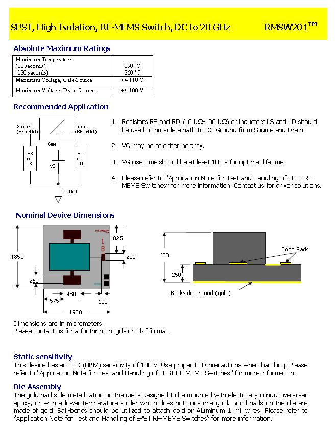
6 The premise of the design is simple. The longer the resonant length of the patch antenna the lower the resonant frequency becomes. The width of the patch antenna controls the impedance of the patch antenna. If we have two nearby patch antennas with small RF switches (RMSW201 MEMS) in between them, biasing the switches will connect the patches together, thus changing the frequency being received. The same switching system can be used to match the impedance of the antenna by adjusting the lengths in the double stub impedance matching network. Therefore, we can use identical RF switches in interconnecting the patch antennas and to also interconnect an impedance matching network stub. The biasing signals of the patch antenna switches and impedance matching network switches can use the same signal to alter the frequency being received by the reconfigurable antenna. This switching will be done through a +5V to -90V DC-DC Converter to bias the RMSW201 MEMS Switch. MEMS Operation: The operation of MEM switches is relatively simple. Like a MOSFET, there are gate, drain, and source terminals. There is a cantilever beam connected to the source and floats above the gate and drain (refer to Figure 6-1). When a biasing voltage (gate-source voltage of +/- 90VDC) is applied to the gate, the difference in voltage creates an attraction that pulls the cantilever beam down to the drain causing a source to drain connection. In other words, when the switch is biased, patch 1 is connected to patch 2. Figure 6-1: RMSW201 MEMS Cantilever beam diagram. A gate to source voltage of +/- 90VDC brings the cantilever beam down to contact the drain. In order to use MEMS for our application, we must insure that the DC voltage of the source and drain are 0VDC while minimizing interference with any RF voltages. This will give a stable gate to source voltage for the switch. This can be done by adding in large resistors or inductors from the
7 source and drain (Patch 1 and Patch 2) to DC ground. According to the MEMS manufacturer RadantMEMS, a resistance of 40kΩ to 100kΩ is suggested for the source and drain (refer to Figure 7-1). 100kΩ will be used to minimize the effects on the RF signals present in the antenna. Figure 7-1: RMSW201 MEMS suggested load resistors or inductor placement to stabilize the DC voltages of the source and drain to 0VDC. Patch Antenna Design: Our patch antenna was designed based upon an ideal rectangular patch antenna. Initially two rectangular patches were designed, one for each desired frequency. The width for each was held constant but calculated based upon Ghz and the RO3010, by use of the following equation: W = c/(2f o * ((ε r +1)/2)). The width that was calculated was mm, this width was used to maintain proper impedance matching. Next length for each patch was determined through the following equation: L = c/(2f o * (ε r )) 2ΔL where ΔL is defined: ΔL = 0.412h*[(ε eff + 0.3)(W/h )]/[( ε eff 0.258)(W/h + 0.8)]. From these equations are Lengths were determined to be L = mm & L = mm. After these calculations were made both antennas were designed in ADS and simulated to check for proper resonance and adjust the measurements to ensure proper resonance. After the two rectangular patch antennas were created initial implementation of a singular reconfigurable antenna began. The design allowed for the initial patch to maintain 40.25mm width and an adjusted length of 29.98mm with a gap of roughly 3mm for MEMS implementation and a secondary patch that was tuned to the size of 1mm in length with a width of mm. This took several iterations to ensure the proper values of each patch to maintain proper resonance. To properly simulate both patches we assumed a simple wire connection between the two patches for 1.227Ghz and an open gap for 1.575Ghz, as seen on the next page.
 Inset Feed Design: For finalized patch antenna design we needed to implement a matching network that would allow for a match to a 50Ω microstrip line.")

 For inset feed matching the following values needed to be determined: Thickness of the mircostrip feed line (W o ), the inset feed width (W 1 ), and the inset feed length (y 0 ).")
8 Figure 8-1: Patch Antenna design for simulation before Inset feed: (left) (right) Inset Feed Design: For finalized patch antenna design we needed to implement a matching network that would allow for a match to a 50Ω microstrip line. To do this we determined it would be best to use inset feed matching. For inset feed matching a microstrip line is inserted into a small slit into the middle of the rectangular patch, the size of the slit and location of the feed point determine the impedance that is matched. Figure 8-2: Rectangular Patch Antenna with Inset Feed line (courtesy For inset feed matching the following values needed to be determined: Thickness of the mircostrip feed line (W o ), the inset feed width (W 1 ), and the inset feed length (y 0 ). To properly match our impedance to 50Ω the Z in also had to be determined at the feed point, which was determined from our rectangular patch simulation (can be found in the simulations section). Based upon our W o of 0.6mm for a 50Ω line this was then used as the W 1 value as well. Lastly, to determine y 0 the following equation was used: y 0 = [Cos -1 (Z 0 /Z in )] 2 *(L/π)
9 This gave us a y 0 of 10.2mm. After tuning and adjustments the finalized patch with inset feed was designed and can be seen below: Chapter 2 Conclusions: In order to keep this design simple, the reconfigurable antenna will be designed using a linear microstrip patch antenna. The preferred switching method will be MEMS switches due to accuracy and small package size compared to pin diodes and transistors. If this design can proven, further research can be done to increase efficiency and/or add in circular polarization. Chapter 3: Design, Specifications, and Requirements After thorough research, specifications must be set to insure that the proposed reconfigurable antenna design will be effective enough to complete the desired application. To prove that this design works, two commercially available GPS frequencies will be used as the application. High Level System Block Diagram: Patch 1 (1.575 GHz) Switches? On Patch 2 Connected (1.227 GHz) Off Inset Feed Matches to 50? Output to Coax Connector Figure 9-1: High Level System Block Diagram of Reconfigurable Antenna with Inset Feed Matching. If the 1.575GHz GPS signal is desired, then the switches will be off, holding the patch antenna at the smaller length and thus higher resonant frequency. If the GHz is desired, the switches will be turned on thus closing the connections between the patch antennas, this will adjust the
10 length of both the antenna to resonant at GHz. The operation of the reconfigurable antenna is illustrated in Figure 2-1. Polarization: The GPS frequencies that we will be receiving are transmitted using right-hand circular polarization according to However, to meet project deadlines we will be simplifying our patch antenna design to consist of linear polarization. This means we will use square or rectangular patches without any modifications for polarization (truncated corners, slots, etc.). If we prove the linear polarization design to be possible, it will open up possibilities for future projects to add in right hand circular polarization. Switching Technology: We needed to determine which method of switching will not only be the most plausible but the best for our system. A small switch size is desired to limit the gap size between patch antennas. It is also very important that the RF switches have low insertion loss and high isolation in addition to operation at RF frequencies. Our goal was to implement RF MEMS switches, to meet the project objective. The drawbacks are high cost and high biasing Gate-Source Voltages. We are going to try to implement RadantMEMS RMSW201 MEMS Switches in our patch antenna. Its specifications are: DC to 20 GHz Operation 0.3dB Insertion 2GHz 35dB Isolation 2GHz 1.9mm x 1.85mm package size +/- 90V Gate-Source Voltage Gold Plating on Micro Strip Board required for wire bonding Switching Control System: To bias the MEMS Switches, we need to apply a +/- 90V to the Gate-Source of the switches. For the patch antenna system, the switches will either be all on or all off. We will be using only 2 MEMS Switches for the antenna system between the 2 patches. Since we are using inset feed matching, no MEMS switches will be required for the impedance matching.
11 Functional Requirements and Specifications: Antenna System: The first patch antenna shall have a center resonant frequency of 1.575GHz, impedance of 50 ohms, and Linear Polarization. The connected patch antennas shall have a combined center resonant frequency of 1.227GHz, impedance of 50 ohms, and Linear Polarization. The patch antenna area shall be kept small without sacrificing too much performance. Switching System: The switch package size shall be less than or equal to 2.0mm (for length) to ensure close proximity of patch antennas. The switches shall have a Low Insertion Loss ( 2GHz). The switches shall have a High Isolation loss ( The switches shall operate at least within 1 to 2 GHz frequency range. The switches shall have a fast switching speed ( <10us). Substrate: The substrate shall have a high dielectric constant, εr (~10). The substrate shall have as small of thickness as possible without sacrificing durability ( > 10mils). The substrate shall minimize the bandwidth around the resonant frequencies to reject noise of outside frequencies while meeting the minimum bandwidth required for GPS GHz Bandwidth is GHz to GHz GHz Bandwidth is GHz to GHz The microstrip board shall be gold plated in the areas where wire bonding is required for the MEMS switches. Equipment List (For 1 Reconfigurable Antenna): From RadantMEMS: o 2 RMSW201 MEMS Switches o 1 +/-90 V DC-DC Converter From Rogers Corporation: o RO x18 High Frequency Laminate Chapter 3 Conclusions: With the design criteria and specifications in place, the physical design and simulations of the reconfigurable patch antenna can begin.
12 Chapter 4: Schematics and Layouts This project had 3 separate circuits or layouts designed and fabricated. First off was an evaluation board of the RMSW201 MEMS switch to determine S-Parameters, but more importantly the effects of the ground pad on the bottom side of the MEMS switch. The second circuit constructed was the +/-90V DC-DC converter that controls the biasing of the MEMS switches. This schematic was obtained through RadantMEMS datasheet for the PCB version of the DC-DC converter, but it was built on a breadboard in lab. The final layout is the actual patch antenna system with inset feed matching. All three of these layouts combine to create the final project. RMSW201 MEMS Evaluation Board: The evaluation board is designed for a Roger s Corporation RO mil substrate, the same substrate the antenna system uses. Its purpose is to determine the effects of the ground pad on the received signal. In order to do this, three separate orientations are used for the switch (refer to Figure 13-1). First is a 2.0mmX2.0mm landing pad with vias to the ground layer of the substrate. Conductive epoxy is used between the landing pad and the MEMS ground pad to create a solid connection to the board both mechanically and electrically. The worry is that this ground pad will interfere with the RF signal crossing the source and drain of the switch. Possible alternatives to this are included in the two other orientations on the evaluation board. One option is a floating ground pad for the MEMS switch. It is the same as the previously mentioned orientation, but there are no vias to the ground plane of the substrate. Conductive epoxy will still be used. The final alternative option is to sand off the ground pad of the MEMS switch. The switch is then attached to the evaluation board with nonconductive double-sided thermal tape. No landing pad will be present on evaluation board. This will minimize the amount of copper that can potentially interfere with the received signals. On the evaluation board, the transmission lines are 23.45mils wide to create a 50Ω line. A 50Ω calibration line is at the top of the board to be used when connected to the spectrum analyzer. Coax connectors are added to each port with a landing pattern specific for the Emerson connector. 8 total coax connectors are used on the evaluation board. Also, each source and drain line has a 100kΩ surface mount resistor (1.6mmX0.8mm) to the ground plane through a via hole. A 200milX200mil pad is connected to the gate of each switch to allow a wire to be soldered to the pad. This will be connected to the DC-DC converter allowing the switches to be biased when needed. The transmission line width here is arbitrary since the signal is DC and the switch draws no current.
.")
13 Figure 13-1: Fabricated Layout of the RMSW201 MEMS Evaluation Board. DC-DC Converter: The RMSW201 MEMS switch requires a gate to source biasing voltage of +/-90VDC to connect the source and drain. In order to do this, we recreated the +5V to -90V DC-DC converter available from RadantMEMS on a breadboard (refer to Figure 14-1 for schematic). The voltage output of MAX774 is determined by the ratio of the feedback resistors (R2/R1) = (Vout/Vref) where Vref is 1.5V. The value of R2 is determined by R2 = (Vout/10uA); in other words, the value of R2 is 9.1MΩ. For this DC-DC converter, R1 is 150kΩ and R2 is 9.1MΩ creating an output voltage of -91V. When the p-channel MOSFET is on, the energy is stored in the inductor L1. When the voltage across the inductor L1 exceeds 210mV, an internal voltage comparator indirectly measures the current going through the MOSFET and shuts off the MOSFET. This discharges the inductor energy to ground causing the capacitor C4 to charge to -90V. If the voltage of the drain falls below 4.8VDC, then the process repeats to maintain the -90VDC output.
14 Figure 14-1: Schematic of RMSW201 MEMS +5V to -90V DC-DC Converter. Patch Antenna System with Inset Feed Matching: The finalized patch antenna will contain both patches to ensure proper frequency configurability. Along with these patches various components will be added for testing, switching, and implementation purposes. The patch and inset feed microstrip line are of the same dimensions as discussed in chapter 3, however the feed line was extended to allow for the addition of a single port coaxial connector. Similarly, to ground pads were added at this same port for proper coax connections. Secondly the additions of two small ground pads were added to the right of each patch length to allow for the addition of a RF resistor for each patch. These resistors will eliminate any noise and excess current flow at lower frequencies to prevent any errors with our GPS frequencies. Lastly a feed line was added to supply the gate portion of the MEMS switches with -90V DC. The feed lines are commonly connected to a single pad at the top of the antenna where the DC to DC converter output will be attached. At the opposite end of the gate feed lines is a small gate pad to allow for proper wire bonding to the MEMS device. Also there will be two antenna types manufactured, both shown on the following page. One will contain two 2x2mm landing pads for the MEMS switches (located between the gap and next to the feed lines), the other will not contain these pads.


15 Figure 15-1: Finalized Layout of the Frequency Reconfigurable Microstrip Patch Antenna Without Landing Pads. Figure 15-2: Finalized Layout of the Frequency Reconfigurable Microstrip Patch Antenna With Landing Pads. Chapter 4 Conclusions: The next step is to simulate and tune the results of the patch antenna system layout until the desired results are achieved. The DC-DC converter will be tested and built on a breadboard while the MEMS evaluation board is simple enough to skip simulations and go to fabrication.
16 Chapter 5: Simulation Results In this chapter you will find the simulation results for the discussed layouts in chapter 3. These simulations were done through ADS Momentum with the patch antenna dimensions as described. Various simulations were done to better tune and adjust patch L, W, and inset feed matching; these results represent our final simulations both before and after inset feed implementation. Note: Some dimensions (length and width) were adjusted after addition of inset feed line GHz (without inset feed matching) Figure 16-1: Simulation results for Ghz patch without inset feed match
17 Figure 17-1: Data set, simulation results for Ghz patch without inset feed match GHz (without inset feed matching) Figure 17-2: Simulation results for Ghz patch without inset feed match
18 Figure 18-1: Simulation results (and data set) for Ghz patch without inset feed match

 Figure 19-2: 227 Ghz")
19 1.575 GHz (with inset feed matching) Figure 19-1: Simulation & data set for Ghz with inset feed matching GHz (with inset feed matching) Figure 19-2: Simulation & data set for Ghz with inset feed matching

20 Chapter 6: Test Results and Simulation Comparison As the end of the semester came about at the same time as our fabrication, the procedure to demonstrate our project changed. We wanted to demonstrate our two resonant frequencies and DC-DC Converter. In order to do this, one antenna system remained unchanged to resonate at GHz. Another antenna system was modified by soldering 2 wires between the patches to represent a closed MEMS switch (1.227 GHz). DC-DC Converter Results: Figure 20-1: Oscilloscope plot of the DC-DC Converter switching from 0V (Ground) to -90V (when Vin is +5V). The DC-DC inverting boost converter successfully switches between 0V and ~-92V pending the Vin voltage GHz Results: The results for our GHz patch antenna was obtained via spectrum analyzer to find the S11 parameters of the antenna. These results can be compared to our simulated data. The antenna used is shown in Figure The results are shown in Figure The actual resonant frequency is shown in blue (1.515 GHz) while the target resonant frequency is shown in red (1.575 GHz). The resonant frequency is 60 MHz lower than the target frequency. The db at the resonant frequency is about -10dB, which is not as strong of a signal as the simulation data due to the inset feed being set up to match GHz.

21 Figure 21-1: GHz antenna system used to obtain Test Results. Figure 21-2: GHz Test Results.

22 1.227 GHz Results: In order to simulate closed MEMS switches, two wires were soldered across the location where the MEMS switches would be placed. These connections changed the resonant frequency. Figure 22-1: GHz antenna system using 2 wires to simulate closed MEMS switches. Figure 22-2: GHz Test Results
23 From the results, GHz is the actual resonant frequency while GHz is the target frequency. Again, the resonant frequency is about 50 to 60 MHz off, but this time it is a higher than the target frequency. The db of the resonant frequency is about -8dB, which is not as strong as expected due to the inset feed being set up for GHz. Chapter 7: Conclusion Testing with MEMS switches will follow, but at the moment the antenna system behaves almost as intended beyond the resonant frequency locations. However, a larger bandwidth could have fixed these problems. This could be done with a thicker substrate or lower dielectric constant. Determining the cause of the change in resonant frequency will come with later testing. Recommendations: The design behind the reconfigurable patch antenna has many possibilities for future work. First off, circular polarization can be added by truncated corners, slots, etc. It was dropped from the project due to time constraints and complexity it presented. Some preliminary work was done to show it was feasible, but the goal was to produce a working frequency reconfigurable antenna by the end of the semester. In addition, a single stub or double stub impedance matching network could be used instead of inset feed matching. While not entirely necessary, at different application frequencies these impedance matching networks will give more accurate matching for each resonant frequency. The downfall of these matching networks compared to inset feed matching is the complexity and physical size added into the project. For final fabrication and design of the patch antenna, due to variances between simulations and tests, it is suggested that multiple designs are made of the antenna. For these designs some patches should be made to resonant slightly higher than desired, some at desired, and some below desired during simulations. These, when fabricated, will help determine the final dimensions to be used for final product fabrication and thus will help eliminate any variances, like the ~60Mhz differences we noticed. Lastly, newer MEMS switches with smaller package sizes and/or lower biasing voltages can be picked for the antenna system. With the RMSW201, removing the ground plane with sandpaper is not a practical design choice. Also, a third MEMS switch could be added to improve connectivity between patches.
24 References: Application Note for MAX774 DC-to-DC Converter. RadantMEMS, Web. Nov < Application Note for Test & Handling of SPST RF-MEMS Switches. RadantMEMS, Web. Nov < Balanis, Constantine A. Antenna Theory: Analysis and Design. 3rd ed. Hoboken, NJ: John Wiley, Print. DeSignor, Jessica A., and Jayanti Venkataraman. "Reconfigurable Dual Frequency Microstrip Patch Antenna Using RF MEMS Switches." IEEE Xplore. May Web. 20 Sept Rebeiz, Gabriel M., and Jeremy B. Muldavin. "RF MEMS Switches and Switch Circuits." IEEE Xplore. Dec Web. 20 Sept SPST, High-Isolation, RF-MEMS Switch DC to 20 GHz. RadantMEMS, Web. 28 Oct < Taslimi, Pejman. "Patch Antenna Analysis Using Ansoft Designer." Shahed University of Tehran, Aug Web. Feb < Yang, Songnan, Chunna Zhang, Helen K. Pan, Aly E. Fathy, and Vijay K. Nair. "Frequency Reconfigurable Antennas for Multiradio Wireless Platforms." IEEE Microwave Magazine (2009): Print.
25 Appendix: 1. RMSW201 MEMS Switch Datasheet Application Note for Testing and Handling of MEMS Application Note for MAX774 DC-to-DC Converter Rogers Corporation RO3000 Series Datasheet Panasonic SMT Resistor s Recommended Land Pattern Emerson SMA 50Ω Coaxial Connector Datasheet

26
27

28
29
30

31
32
33
34

35

36
37
38
39
40
41
42
43

44
Reconfigurable Antenna with Matching Network Project Proposal. Students: Mike Bly, Josh Rohman Advisor: Dr. Prasad N. Shastry Date: November 29, 2011
 Reconfigurable Antenna with Matching Network Project Proposal Students: Mike Bly, Josh Rohman Advisor: Dr. Prasad N. Shastry Date: November 29, 2011 Introduction: The goal of this project is to develop
IEEE Antennas and Wireless Propagation Letters. Copyright Institute of Electrical and Electronics Engineers.
 Title Dual-band monopole antenna with frequency-tunable feature for WiMAX applications Author(s) Sun, X; Cheung, SW; Yuk, TTI Citation IEEE Antennas and Wireless Propagation Letters, 2013, v. 12, p. 100-103
Chapter 5 DESIGN AND IMPLEMENTATION OF SWASTIKA-SHAPED FREQUENCY RECONFIGURABLE ANTENNA ON FR4 SUBSTRATE
 Chapter 5 DESIGN AND IMPLEMENTATION OF SWASTIKA-SHAPED FREQUENCY RECONFIGURABLE ANTENNA ON FR4 SUBSTRATE The same geometrical shape of the Swastika as developed in previous chapter has been implemented
COMPACT SLOT ANTENNA WITH EBG FEEDING LINE FOR WLAN APPLICATIONS
 Progress In Electromagnetics Research C, Vol. 10, 87 99, 2009 COMPACT SLOT ANTENNA WITH EBG FEEDING LINE FOR WLAN APPLICATIONS A. Danideh Department of Electrical Engineering Islamic Azad University (IAU),
Evaluation of Modeling Accuracy of Reconfigurable Patch Antennas
 International Journal of Scientific and Research Publications, Volume 4, Issue 11, November 2014 1 Evaluation of Modeling Accuracy of Reconfigurable Patch Antennas Mr. Ullhas.Jayakumar.Maisale *, Prof.
Monopole Plannar Antenna Using Switchable Slot Structures
 Monopole Plannar Antenna Using Switchable Slot Structures Manoj K C Assistant Professor Department of ECE Vimal Jyothi Engineering College, Chemperi, Kannur, Kerala, India Stephy John PG Scholar Department
Reconfigurable Low Profile Patch Antenna
 Bradley University Department of Electrical and Computer Engineering Reconfigurable Low Profile Patch Antenna Mr. James H. Soon Advisor: Dr. Prasad Shastry May 13, 2005 Abstract The objective of this project
UNIVERSITI MALAYSIA PERLIS
 UNIVERSITI MALAYSIA PERLIS SCHOOL OF COMPUTER & COMMUNICATIONS ENGINEERING EKT 341 LABORATORY MODULE LAB 2 Antenna Characteristic 1 Measurement of Radiation Pattern, Gain, VSWR, input impedance and reflection
DESIGN OF RECONFIGURABLE PATCH ANTENNA WITH A SWITCHABLE V-SLOT
 Progress In Electromagnetics Research C, Vol. 6, 145 158, 2009 DESIGN OF RECONFIGURABLE PATCH ANTENNA WITH A SWITCHABLE V-SLOT T. Al-Maznaee and H. E. Abd-El-Raouf Department of Electrical and Computer
DESIGN AND DEVELOPMENT OF MICROSTRIP PATCH ANTENNA
 DESIGN AND DEVELOPMENT OF MICROSTRIP PATCH ANTENNA ABSTRACT Aishwarya Sudarsan and Apeksha Prabhu Department of Electronics and Communication Engineering, NHCE, Bangalore, India A Microstrip Patch Antenna
Investigating the effects of control lines on a frequency reconfigurable patch antenna
 Loughborough University Institutional Repository Investigating the effects of control lines on a frequency reconfigurable patch antenna This item was submitted to Loughborough University's Institutional
Design and Improved Performance of Rectangular Micro strip Patch Antenna for C Band Application
 RESEARCH ARTICLE OPEN ACCESS Design and Improved Performance of Rectangular Micro strip Patch Antenna for C Band Application Vinay Jhariya*, Prof. Prashant Jain** *(Department of Electronics & Communication
SDARS: Front End Antenna Design. Keven Lockwood Advisor: Dr. Prasad Shastry
 SDARS: Front End Antenna Design Keven Lockwood Advisor: Dr. Prasad Shastry 1 Outline Project Overview Antenna Characteristics Feeding Techniques Performance Specifications Design Process Expected results
Design of Reconfigurable Rectangular Patch Antenna using PIN Diode
 International Journal of Electrical Sciences & Engineering (IJESE) Online ISSN: 2455 6068; Volume 1, Issue 1; January 2016 pp. 68-73 Dayananda Sagar College of Engineering, Bengaluru-78 Design of Reconfigurable
Fractal Reconfigurable Multiband Communicating Antenna for Cognitive Radio
 IOSR Journal of Electronics and Communication Engineering (IOSR-JECE) e-issn: 2278-2834,p- ISSN: 2278-8735.Volume 10, Issue 1, Ver. III (Jan - Feb. 2015), PP 49-56 www.iosrjournals.org Fractal Reconfigurable
SDARS Receiver Front-End
 SDARS Receiver Front-End Project Proposal Keven Lockwood Dr. Prasad Shastry December 9, 2010 Project Summary This project focuses on the front-end receiver design for the Satellite Digital Audio Radio
Reconfigurable Microstrip Antenna Array Vidya B. Babare1, S. B. Deosarkar2 E&TC Department, Pune University1,2 VPCOE Baramati
 Reconfigurable Microstrip Antenna Array Vidya B. Babare1, S. B. Deosarkar2 E&TC Department, Pune University1,2 VPCOE Baramati Abstract A reconfigurable antenna is another solution to achieve a wide impedance
CHAPTER 3 DESIGN OF MICROSTRIP PATCH ARRAY ANTENNA
 CHAPTER 3 DESIGN OF MICROSTRIP PATCH ARRAY ANTENNA 3.1 Introduction This chapter is discussed on the various factors that affect the design of microstrips patch array antenna. This chapter will covered
Recon UWB Antenna for Cognitive Radio
 Progress In Electromagnetics Research C, Vol. 79, 79 88, 2017 Recon UWB Antenna for Cognitive Radio DeeplaxmiV.Niture *, Santosh S. Jadhav, and S. P. Mahajan Abstract This paper talks about a simple printed
Antenna Theory and Design
 Antenna Theory and Design Antenna Theory and Design Associate Professor: WANG Junjun 王珺珺 School of Electronic and Information Engineering, Beihang University F1025, New Main Building wangjunjun@buaa.edu.cn
Rectangular Patch Antenna to Operate in Flame Retardant 4 Using Coaxial Feeding Technique
 International Journal of Electronics Engineering Research. ISSN 0975-6450 Volume 9, Number 3 (2017) pp. 399-407 Research India Publications http://www.ripublication.com Rectangular Patch Antenna to Operate
Sree Vidyanikethan Engineering College, Tirupati, India 3.
 Volume 114 No. 10 2017, 301-308 ISSN: 1311-8080 (printed version); ISSN: 1314-3395 (on-line version) url: http://www.ijpam.eu ijpam.eu Design and Simulation Of Circular Patch Log Periodic Microstrip Antenna
10 GHz LNA for Amateur Radio by K5TRA
 Introduction Ham radio operation on 10 GHz is somewhat exotic. This is far removed from global short-wave communication below 30 MHz, or regional VHF and UHF communication. Despite the arcane nature of
Proximity Coupled Equilateral Triangular Microstrip Antenna with Diamond Shape Slot for Dual Band Operation
 Proximity Coupled Equilateral Triangular Microstrip Antenna with Diamond Shape Slot for Dual Band Operation Mahesh C. P 1, P. M. Hadalgi 2 Research Scholar, Department of P.G. Studies and Research in Applied
Tri Band Dual Polarized Patch Antenna System For Next Generation Cellular Networks
 Tri Band Dual Polarized Patch Antenna System For Next Generation Cellular Networks Syed Daniyal Ali Shah Abstract: In fifth generation networks, much emphasis is given to reduce the handset and base station
Designing of Rectangular Microstrip Patch Antenna for C-Band Application
 International OPEN ACCESS Journal Of Modern Engineering Research (IJMER) Designing of Rectangular Microstrip Patch Antenna for C-Band Application Vinay Jhariya 1, Prof. Prashant Jain 2 1,2 Department of
Circular Patch Antenna with CPW fed and circular slots in ground plane.
 Circular Patch Antenna with CPW fed and circular slots in ground plane. Kangan Saxena, USICT, Guru Gobind Singh Indraprastha University, Delhi-75 ---------------------------------------------------------------------***---------------------------------------------------------------------
Dual Feed Microstrip Patch Antenna for Wlan Applications
 IOSR Journal of Electronics and Communication Engineering (IOSR-JECE) e-issn: 2278-2834,p- ISSN: 2278-8735.Volume 10, Issue 5, Ver. I (Sep - Oct.2015), PP 01-05 www.iosrjournals.org Dual Feed Microstrip
Inset Fed Microstrip Patch Antenna for X-Band Applications
 Inset Fed Microstrip Patch Antenna for X-Band Applications Pradeep H S Dept.of ECE, Siddaganga Institute of Technology, Tumakuru, Karnataka. Abstract Microstrip antennas play an important role in RF Communication.
Application Note 5011
 MGA-62563 High Performance GaAs MMIC Amplifier Application Note 511 Application Information The MGA-62563 is a high performance GaAs MMIC amplifier fabricated with Avago Technologies E-pHEMT process and
DESIGN AND IMPLEMENTATION OF RECONFIGURABLE PATCH ANTENNAS FOR WIRELESS COMMUNICATIONS
 University of Nebraska - Lincoln DigitalCommons@University of Nebraska - Lincoln Theses, Dissertations, and Student Research from Electrical & Computer Engineering Electrical & Computer Engineering, Department
Optically reconfigurable balanced dipole antenna
 Loughborough University Institutional Repository Optically reconfigurable balanced dipole antenna This item was submitted to Loughborough University's Institutional Repository by the/an author. Citation:
Design of Z-Shape Microstrip Antenna with I- Slot for Wi-Max/Satellite Application
 Journal of Communication and Computer 13 (2016) 261-265 doi:10.17265/1548-7709/2016.05.006 D DAVID PUBLISHING Design of Z-Shape Microstrip Antenna with I- Slot for Wi-Max/Satellite Application Swarnaprava
ISSN: ISO 9001:2008 Certified International Journal of Engineering Science and Innovative Technology (IJESIT) Volume 6, Issue 4, July 2017
 Volume 6, Issue 4, July 2017") Design of circularly polarized micro strip patch array antenna using RT DUROID, POLYSTERENE & FR4 EPOXY substrate materials for Bluetooth and wlan applications 1 POORNA PRIYA, 2 A. SRIVANI, 3 M. SAI CHANDRIKA,
Design of circularly polarized micro strip patch array antenna using RT DUROID, POLYSTERENE & FR4 EPOXY substrate materials for Bluetooth and wlan applications 1 POORNA PRIYA, 2 A. SRIVANI, 3 M. SAI CHANDRIKA,
International Journal of Microwaves Applications Available Online at
 ISSN 2320-2599 Volume 6, No. 3, May - June 2017 Sandeep Kumar Singh et al., International Journal of Microwaves Applications, 6(3), May - June 2017, 30 34 International Journal of Microwaves Applications
AN APPROACH TO DESIGN AND OPTIMIZATION OF WLAN PATCH ANTENNAS FOR WI-FI APPLICATIONS
 IJWC ISSN: 31-3559 & E-ISSN: 31-3567, Volume 1, Issue, 011, pp-09-14 Available online at http://www.bioinfo.in/contents.php?id109 AN APPROACH TO DESIGN AND OPTIMIZATION OF WLAN PATCH ANTENNAS FOR WI-FI
Implementation and Applications of Various Feeding Techniques Using CST Microwave Studio
 Implementation and Applications of Various Feeding Techniques Using CST Microwave Studio Dr Sourabh Bisht Graphic Era University sourabh_bisht2002@yahoo. com Ankita Singh Graphic Era University ankitasingh877@gmail.com
Ultra-Wideband Patch Antenna for K-Band Applications
 TELKOMNIKA Indonesian Journal of Electrical Engineering Vol. x, No. x, July 214, pp. 1 5 DOI: 1.11591/telkomnika.vXiY.abcd 1 Ultra-Wideband Patch Antenna for K-Band Applications Umair Rafique * and Syed
Analysis of a Co-axial Fed Printed Antenna for WLAN Applications
 Analysis of a Co-axial Fed Printed Antenna for WLAN Applications G.Aneela 1, K.Sairam Reddy 2 1,2 Dept. of Electronics & Communication Engineering ACE Engineering College, Ghatkesar, Hyderabad, India.
Design of Controlled RF Switch for Beam Steering Antenna Array
 PIERS ONLINE, VOL. 4, NO. 3, 2008 356 Design of Controlled RF Switch for Beam Steering Antenna Array M. M. Abusitta, D. Zhou, R. A. Abd-Alhameed, and P. S. Excell Mobile and Satellite Communications Research
Design a Reconfigurable Patch Antenna for Mobile Application
 Design a Reconfigurable Patch Antenna for Mobile Application Prashant Chandra Bhardwaj 1 M.Tech Scholar Arya Inst.Of Engg. And Technology, Jaipur Prashantbhardwaj.rtu@gmail.com Ashok Kumar Kajla 2 Associate
Design of Frequency and Polarization Tunable Microstrip Antenna
 Design of Frequency and Polarization Tunable Microstrip Antenna M. S. Nishamol, V. P. Sarin, D. Tony, C. K. Aanandan, P. Mohanan, K. Vasudevan Abstract A novel compact dual frequency microstrip antenna
Antenna Matching Within an Enclosure Part II: Practical Techniques and Guidelines
 Antenna Matching Within an Enclosure Part II: Practical Techniques and Guidelines By Johnny Lienau, RF Engineer June 2012 Antenna selection and placement can be a difficult task, and the challenges of
Circularly Polarized Square Patch Microstrip Antenna with Y- Shaped Slot for Wi-Max Application
 Available online www.ejaet.com European Journal of Advances in Engineering and Technology, 2014, 1(1): 61-68 Research Article Circularly Polarized Square Patch Microstrip Antenna with Y- Shaped Slot for
Chapter 2. Modified Rectangular Patch Antenna with Truncated Corners. 2.1 Introduction of rectangular microstrip antenna
 Chapter 2 Modified Rectangular Patch Antenna with Truncated Corners 2.1 Introduction of rectangular microstrip antenna 2.2 Design and analysis of rectangular microstrip patch antenna 2.3 Design of modified
Comparative Analysis of Microstrip Rectangular Patch Antenna with Different Feeding Techniques using HFSS
 Mody University International Journal of Computing and Engineering Research Vol. 1 Issue 1, 2017, pp.34-42 ISSN: 2456-9607 (Print) 2456-8333(Online) Comparative Analysis of Microstrip Rectangular Patch
Application Note 5525
 Using the Wafer Scale Packaged Detector in 2 to 6 GHz Applications Application Note 5525 Introduction The is a broadband directional coupler with integrated temperature compensated detector designed for
Microstrip Bandpass Filter with Notch Response at 5.2 GHz using Stepped Impedance Resonator
 International Journal of Engineering Research and Technology. ISSN 0974-3154 Volume 11, Number 3 (2018), pp. 417-426 International Research Publication House http://www.irphouse.com Microstrip Bandpass
DESIGN AND ANALYSIS OF RECTANGULAR MICROSTRIP PATCH ANTENNA USING METAMATERIAL FOR BETTER EFFICIENCY
 DESIGN AND ANALYSIS OF RECTANGULAR MICROSTRIP PATCH ANTENNA USING METAMATERIAL FOR BETTER EFFICIENCY Gourav Singh Rajput, Department of Electronics, Madhav Institute of Technology and Science Gwalior,
H And U-Slotted Rectangular Microstrip Patch Antenna
 H And U-Slotted Rectangular Microstrip Patch Antenna Bharat Rochani 1, Sanjay Gurjar 2 1 Department of Electronics and Communication Engineering, Engineering College Ajmer 2 Department of Electronics and
Application Note 1360
 ADA-4743 +17 dbm P1dB Avago Darlington Amplifier Application Note 1360 Description Avago Technologies Darlington Amplifier, ADA-4743 is a low current silicon gain block RFIC amplifier housed in a 4-lead
A HIGH GAIN DUAL BAND RECONFIGURABLE STACKED MICROSTRIP ANTENNA FOR WIRELESS APPLICATIONS
 A HIGH GAIN DUAL BAND RECONFIGURABLE STACKED MICROSTRIP ANTENNA FOR WIRELESS APPLICATIONS V. Shanthi 1, G. Sreedhar Kumar 2, Y. Anusha 3 1,2,3 Department of electronics and communication Engineering, G.Pullaiah
Figure 1 Schematic diagram of a balanced amplifier using two quadrature hybrids (eg Lange Couplers).
.") 1 of 14 Balanced Amplifiers The single amplifier meets the specification for noise figure and again but fails to meet the return loss specification due to the large mis-matches on the input & outputs.
1 of 14 Balanced Amplifiers The single amplifier meets the specification for noise figure and again but fails to meet the return loss specification due to the large mis-matches on the input & outputs.
Frequency Reconfigurable Micro-strip Patch Antenna for Wideband Applications
 Frequency Reconfigurable Micro-strip Patch Antenna for Wideband Applications Monika Arora, Suman Abstract A frequency reconfigurable microstrip patch antenna is presented in this paper. The antenna is
Design & Simulation of Circular Patch Antennafor Multiband application of X Band UsingVaractor Diodes
 Conference on Advances in Communication and Control Systems 2013 (CAC2S 2013) 1 Design & Simulation of Circular Patch Antennafor Multiband application of X Band UsingVaractor Diodes Pawan Pujari Student,
ECE 4370: Antenna Design Fall 2012 Design Project: 5.8 GHz High-Directivity Antenna Ryan Bahr, David Giles, Brian Palmer, Dan Russo
 ECE 4370: Antenna Design Fall 2012 Design Project: 5.8 GHz High-Directivity Antenna Ryan Bahr, David Giles, Brian Palmer, Dan Russo Specifications: The antenna was required to operate with linear polarization
Design Approach of a Wideband Frequency Tunable Triangular Patch Array with Concurrent Polarization Alteration
 Design Approach of a Wideband Frequency Tunable Triangular Patch Array with Concurrent Polarization Alteration Biswajit Dwivedy 1 and Santanu Kumar Behera 2 Department of Electronics and Communication
Miniature Multiband Antenna for WLAN and X-Band Satellite Communication Applications
 Progress In Electromagnetics Research Letters, Vol. 75, 13 18, 2018 Miniature Multiband Antenna for WLAN and X-Band Satellite Communication Applications Ruixing Zhi, Mengqi Han, Jing Bai, Wenying Wu, and
Design of Microstrip Patch Antenna for GPS Applications using EBG Structures
 Design of Microstrip Patch Antenna for GPS Applications using EBG Structures Naveen JVSS 1, Varun Kumar.K 2, Ramesh.B 3, Vinay. K.P 4 Department of E.C.E, Raghu Engineering College, Visakhapatnam, Andhra
Application Note 1299
 A Low Noise High Intercept Point Amplifier for 9 MHz Applications using ATF-54143 PHEMT Application Note 1299 1. Introduction The Avago Technologies ATF-54143 is a low noise enhancement mode PHEMT designed
INVENTION DISCLOSURE- ELECTRONICS SUBJECT MATTER IMPEDANCE MATCHING ANTENNA-INTEGRATED HIGH-EFFICIENCY ENERGY HARVESTING CIRCUIT
 INVENTION DISCLOSURE- ELECTRONICS SUBJECT MATTER IMPEDANCE MATCHING ANTENNA-INTEGRATED HIGH-EFFICIENCY ENERGY HARVESTING CIRCUIT ABSTRACT: This paper describes the design of a high-efficiency energy harvesting
Low Noise Amplifiers for 2304, 3456, 5760, and MHz using the ATF PHEMT by Al Ward WB5LUA
 Low Noise Amplifiers for 2304, 3456, 5760, and 10368 MHz using the by Al Ward INTRODUCTION The Hewlett-Packard device is described in a series of low noise amplifiers for 2304, 3456, 5760, and 10368 MHz.
A Reconfigurable Micro-strip Patch Antenna for Various Wireless and Cognitive Radio Applications
 A Reconfigurable Micro-strip Patch Antenna for Various Wireless and Cognitive Radio Applications Ganesh Babu T.V.J. #1, Rajesh Kumar V.R.S. *2 #1St.Martin s Engineering College, Hyderabad, #2 Sri Devi
Wide-Band Two-Stage GaAs LNA for Radio Astronomy
 Progress In Electromagnetics Research C, Vol. 56, 119 124, 215 Wide-Band Two-Stage GaAs LNA for Radio Astronomy Jim Kulyk 1,GeWu 2, Leonid Belostotski 2, *, and James W. Haslett 2 Abstract This paper presents
High Intercept Low Noise Amplifier for 1.9 GHz PCS and 2.1 GHz W-CDMA Applications using the ATF Enhancement Mode PHEMT
 High Intercept Low Noise Amplifier for 1.9 GHz PCS and 2.1 GHz W-CDMA Applications using the ATF-55143 Enhancement Mode PHEMT Application Note 1241 Introduction Avago Technologies ATF-55143 is a low noise
SLOT-FED SWITCHED PATCH ANTENNA FOR MULTI- PLE FREQUENCY OPERATION. of Birmingham, Edgbaston, Birmingham B15 2TT, UK
 Progress In Electromagnetics Research C, Vol. 36, 91 14, 213 SLOT-FED SWITCHED PATCH ANTENNA FOR MULTI- PLE FREQUENCY OPERATION Ghaith Mansour 1, *, Peter S. Hall 1, Peter Gardner 1, and Mohamad K. Abd
Design of Narrow Slotted Rectangular Microstrip Antenna
 Original Article Design of Narrow Slotted Rectangular Microstrip Antenna Ashok Kajla and Sunita Gawria* Electronics & Communication Department ARYA Institute of Engineering and Technology, Jaipur, Rajasthan,
SIERPINSKI CARPET FRACTAL ANTENNA ARRAY USING MITERED BEND FEED NETWORK FOR MULTI-BAND APPLICATIONS
 SIERPINSKI CARPET FRACTAL ANTENNA ARRAY USING MITERED BEND FEED NETWORK FOR MULTI-BAND APPLICATIONS D. Prabhakar 1, P. Mallikarjuna Rao 2 and M. Satyanarayana 3 1 Department of Electronics and Communication
Application Note 5012
 MGA-61563 High Performance GaAs MMIC Amplifier Application Note 5012 Application Information The MGA-61563 is a high performance GaAs MMIC amplifier fabricated with Avago Technologies E-pHEMT process and
Reconfigurable antenna using photoconducting switches
 Loughborough University Institutional Repository Reconfigurable antenna using photoconducting switches This item was submitted to Loughborough University's Institutional Repository by the/an author. Citation:
Gain Slope issues in Microwave modules?
 Gain Slope issues in Microwave modules? Physical constraints for broadband operation If you are a microwave hardware engineer you most likely have had a few sobering experiences when you test your new
Broadband low cross-polarization patch antenna
 RADIO SCIENCE, VOL. 42,, doi:10.1029/2006rs003595, 2007 Broadband low cross-polarization patch antenna Yong-Xin Guo, 1 Kah-Wee Khoo, 1 Ling Chuen Ong, 1 and Kwai-Man Luk 2 Received 27 November 2006; revised
Preliminary Product Overview
 Preliminary Product Overview Features DC to > 3 GHz Frequency Range 25 Watt (CW), 200W (Pulsed) Max Power Handling Low On-State Insertion Loss, typical 0.3 db @ 3 GHz Low On-State Resistance < 0.75 Ω 25dB
DUAL BAND L-SHAPED MICROSTRIP PATCH ANTENNA FOR 5/9 GHZ
 http:// DUAL BAND L-SHAPED MICROSTRIP PATCH ANTENNA FOR 5/9 GHZ Meenaxi 1, Pavan Kumar Shukla 2 1 Department of Electronics and Communication Engineering, Shri Venkateshwara University, Gajrola, U.P. (India)
A Frequency Reconfigurable Monopole Antenna with Switchable Symmetric Slot Strcture
 IOSR Journal of Electronics and Communication Engineering (IOSR-JECE) e-issn: 2278-2834,p- ISSN: 2278-8735.Volume 10, Issue 4, Ver. III (Jul - Aug.2015), PP 26-30 www.iosrjournals.org A Frequency Reconfigurable
International Journal of Microwaves Applications Available Online at
 ISSN 2320 2599 Volume 4, No.1, January - February 2015 Shilpa K Jose et al., International Journal of Microwaves Applications, 4(1), January - February 2015, 06-10 International Journal of Microwaves Applications
A Compact Band-selective Filter and Antenna for UWB Application
 PIERS ONLINE, VOL. 3, NO. 7, 7 153 A Compact Band-selective Filter and Antenna for UWB Application Yohan Jang, Hoon Park, Sangwook Jung, and Jaehoon Choi Department of Electrical and Computer Engineering,
COMPARATIVE STUDY OF FRACTAL ANTENNA WITH RECTANGULAR MICROSTRIP ANTENNA.
 COMPARATIVE STUDY OF FRACTAL ANTENNA WITH RECTANGULAR MICROSTRIP ANTENNA. 1 Ritu khare, Umesh Barahdiya, 3 D.K Srivastava, 4 Rajat Srivastava Abstract: In the present work the proposed fractal antenna
CPW- fed Hexagonal Shaped Slot Antenna for UWB Applications
 International Journal of Information and Computation Technology. ISSN 0974-2239 Volume 3, Number 10 (2013), pp. 1015-1024 International Research Publications House http://www. irphouse.com /ijict.htm CPW-
A Phase Diversity Printed-Dipole Antenna Element for Patterns Selectivity Array Application
 Progress In Electromagnetics Research Letters, Vol. 78, 105 110, 2018 A Phase Diversity Printed-Dipole Antenna Element for Patterns Selectivity Array Application Fukun Sun *, Fushun Zhang, and Chaoqiang
International Journal for Research in Applied Science & Engineering Technology (IJRASET) Circular Microstrip Patch Antenna for RFID Application
 Circular Microstrip Patch Antenna for RFID Application") Circular Microstrip Patch Antenna for RFID Application Swapnali D. Hingmire 1, Mandar P. Joshi 2, D. D. Ahire 3 1,2,3 E&TC Department, 1 R. H. Sapat COE, Nashik, 2,3 Matoshri COE, Nashik, Savitri Bai Phule
Circular Microstrip Patch Antenna for RFID Application Swapnali D. Hingmire 1, Mandar P. Joshi 2, D. D. Ahire 3 1,2,3 E&TC Department, 1 R. H. Sapat COE, Nashik, 2,3 Matoshri COE, Nashik, Savitri Bai Phule
Department of Electrical Engineering University of North Texas
 Name: Shabuktagin Photon Khan UNT ID: 10900555 Instructor s Name: Professor Hualiang Zhang Course Name: Antenna Theory and Design Course ID: EENG 5420 Email: khan.photon@gmail.com Department of Electrical
Design and Layout of a X-Band MMIC Power Amplifier in a Phemt Technology
 Design and Layout of a X-Band MMIC Power Amplifier in a Phemt Technology Renbin Dai, and Rana Arslan Ali Khan Abstract The design of Class A and Class AB 2-stage X band Power Amplifier is described in
CHAPTER 4 DESIGN OF BROADBAND MICROSTRIP ANTENNA USING PARASITIC STRIPS WITH BAND-NOTCH CHARACTERISTIC
 CHAPTER 4 DESIGN OF BROADBAND MICROSTRIP ANTENNA USING PARASITIC STRIPS WITH BAND-NOTCH CHARACTERISTIC 4.1 INTRODUCTION Wireless communication technology has been developed very fast in the last few years.
A Fractal Slot Antenna for Ultra Wideband Applications with WiMAX Band Rejection
 Jamal M. Rasool 1 and Ihsan M. H. Abbas 2 1 Department of Electrical Engineering, University of Technology, Baghdad, Iraq 2 Department of Electrical Engineering, University of Technology, Baghdad, Iraq
EE4101E: RF Communications. Low Noise Amplifier Design Using ADS (Report)
") EE4101E: RF Communications Low Noise Amplifier Design Using ADS (Report) SEM 1: 2014/2015 Student 1 Name Student 2 Name : Ei Ei Khin (A0103801Y) : Kyaw Soe Hein (A0103612Y) Page 1 of 29 INTRODUCTION The
EE4101E: RF Communications Low Noise Amplifier Design Using ADS (Report) SEM 1: 2014/2015 Student 1 Name Student 2 Name : Ei Ei Khin (A0103801Y) : Kyaw Soe Hein (A0103612Y) Page 1 of 29 INTRODUCTION The
Dual-slot based Rectangular Microstrip Antenna for WiMAX, WCS and C-band Satellite Applications
 Dual-slot based Rectangular Microstrip Antenna for WiMAX, WCS and C-band Satellite Applications Surjit Singh 1, Amrit Kaur 2 M.Tech Student, ECE, Baba Banda Singh Bahadur Engineering College, Fatehgarh
A 2.3/3.3 GHz Dual Band Antenna Design for WiMax Applications
 ITB J. ICT, Vol. 4, No. 2, 2010, 67-78 67 A 2.3/3.3 GHz Dual Band Antenna Design for WiMax Applications Adit Kurniawan, Iskandar & P.H. Mukti School of Electrical Engineering and Informatics, Bandung Institute
Design of Rectangular Micro strip Patch Antenna with circular and rectangular slot in X Band
 International Journal of Advances in Electrical and Electronics Engineering 162 Available online at www.ijaeee.com & www.sestindia.org/volume-ijaeee ISSN: 2319-1112 Design of Rectangular Micro strip Patch
Design of a Rectangular Spiral Antenna for Wi-Fi Application
 Design of a Rectangular Spiral Antenna for Wi-Fi Application N. H. Abdul Hadi, K. Ismail, S. Sulaiman and M. A. Haron, Faculty of Electrical Engineering Universiti Teknologi MARA 40450, SHAH ALAM MALAYSIA
CHAPTER 5 ANALYSIS OF MICROSTRIP PATCH ANTENNA USING STACKED CONFIGURATION
 1 CHAPTER 5 ANALYSIS OF MICROSTRIP PATCH ANTENNA USING STACKED CONFIGURATION 5.1 INTRODUCTION Rectangular microstrip patch with U shaped slotted patch is stacked, Hexagonal shaped patch with meander patch
A WIDEBAND RECTANGULAR MICROSTRIP ANTENNA WITH CAPACITIVE FEEDING
 A WIDEBAND RECTANGULAR MICROSTRIP ANTENNA WITH CAPACITIVE FEEDING Hind S. Hussain Department of Physics, College of Science, Al-Nahrain University, Baghdad, Iraq E-Mail: hindalrawi@yahoo.com ABSTRACT A
Performance Analysis of Different Ultra Wideband Planar Monopole Antennas as EMI sensors
 International Journal of Electronics and Communication Engineering. ISSN 09742166 Volume 5, Number 4 (2012), pp. 435445 International Research Publication House http://www.irphouse.com Performance Analysis
ISSN: [Sherke* et al., 5(12): December, 2016] Impact Factor: 4.116
![ISSN: [Sherke* et al., 5(12): December, 2016] Impact Factor: 4.116](/thumbs/86/93220221.jpg "ISSN: [Sherke* et al., 5(12): December, 2016] Impact Factor: 4.116") IJESRT INTERNATIONAL JOURNAL OF ENGINEERING SCIENCES & RESEARCH TECHNOLOGY COMPACT ULTRA WIDE BAND ANTENNA WITH BAND NOTCHED CHARACTERISTICS. Raksha Sherke *, Ms. Prachi C. Kamble, Dr. Lakshmappa K Ragha
IJESRT INTERNATIONAL JOURNAL OF ENGINEERING SCIENCES & RESEARCH TECHNOLOGY COMPACT ULTRA WIDE BAND ANTENNA WITH BAND NOTCHED CHARACTERISTICS. Raksha Sherke *, Ms. Prachi C. Kamble, Dr. Lakshmappa K Ragha
Effect of Slot Rotation on Rectangular Slot based Microstrip Patch Antenna
 International Journal of Current Engineering and Technology E-ISSN 2277 4106, P-ISSN 2347 5161 2015INPRESSCO, All Rights Reserved Available at http://inpressco.com/category/ijcet Research Article Effect
Surface Mount SOT-363 (SC-70) Package. Pin Connections and Package Marking GND. V dd. Note: Package marking provides orientation and identification.
 Package. Pin Connections and Package Marking GND. V dd. Note: Package marking provides orientation and identification.") GHz V Low Current GaAs MMIC LNA Technical Data MGA-876 Features Ultra-Miniature Package.6 db Min. Noise Figure at. GHz. db Gain at. GHz Single + V or V Supply,. ma Current Applications LNA or Gain Stage
GHz V Low Current GaAs MMIC LNA Technical Data MGA-876 Features Ultra-Miniature Package.6 db Min. Noise Figure at. GHz. db Gain at. GHz Single + V or V Supply,. ma Current Applications LNA or Gain Stage
Effect of Open Stub Slots for Enhancing the Bandwidth of Rectangular Microstrip Antenna
 International Journal of Electronics Engineering, 3 (2), 2011, pp. 221 226 Serials Publications, ISSN : 0973-7383 Effect of Open Stub Slots for Enhancing the Bandwidth of Rectangular Microstrip Antenna
A Wide Band Pattern and Frequency Reconfigurable Microstrip Patch Antenna using Varactors for WLAN Applications
 A Wide Band Pattern and Frequency Reconfigurable Microstrip Patch Antenna using Varacrs for WLAN Applications Ros Marie C Cleetus 1 and Dr.T.Sudha 2 Department of Electronics and Communication Engineering
DESIGN OF A PLANAR MONOPOLE ULTRA WIDE BAND PATCH ANTENNA
 International Journal of Electrical and Electronics Engineering Research (IJEEER) ISSN(P): 2250-155X; ISSN(E): 2278-943X Vol. 4, Issue 1, Feb 2014, 47-52 TJPRC Pvt. Ltd. DESIGN OF A PLANAR MONOPOLE ULTRA
Design of Microstrip Array Antenna for Wireless Communication Application
 IOSR Journal of Engineering (IOSRJEN) e-issn: 2250-3021, p-issn: 2278-8719 Vol. 3, Issue 12 (December. 2013), V1 PP 01-07 Design of Microstrip Array Antenna for Wireless Communication Application Hassan