LLC Resonant Charger with Variable Inductor Control
|
|
|
- Lizbeth Malone
- 6 years ago
- Views:
Transcription

; Instituto de Telecomunicações Coimbra (IT-Coimbra) Coimbra,")
1 Mestrado em Engenharia Eletrotécnica LLC Resonant Charger with Variable Inductor Control Trabalho de Projeto apresentado para a obtenção do grau de Mestre em Engenharia Eletrotécnica Área de Especialização em Automação e Comunicações em Sistemas Industriais Autor Válter de Sousa Costa Orientador Professora Doutora Marina Mendes Sargento Domingues Perdigão Departamento de Engenharia Eletrotécnica Instituto Superior de Engenharia de Coimbra Instituto Politécnico de Coimbra (DEE-ISEC-IPC); Instituto de Telecomunicações Coimbra (IT-Coimbra) Co-Orientador Professor Doutor André Manuel dos Santos Mendes Departamento de Engenharia Eletrotécnica e de Computadores Universidade de Coimbra (DEEC-FCTUC); Instituto de Telecomunicações Coimbra (IT-Coimbra) Coimbra, março, 2017
2
3 ACKNOWLEDGMENTS ACKNOWLEDGMENTS With the conclusion of this work I would like to thank, firstly to Professor Marina Perdigão (Departamento de Engenharia Eletrotécnica Instituto Superior de Engenharia de Coimbra Instituto Politécnico de Coimbra, DEE-ISEC-IPC and Instituto de Telecomunicações Coimbra, IT-Coimbra) and Professor André Mendes (IT-Coimbra and, Departamento de Engenharia Eletrotécnica e de Computadores Universidade de Coimbra, DEEC-UC) for guiding me and helping me in order to complete this work. To ISEC-IPC that received me and, where I took by bachelor degree in Electrotechnical Engineering and where I am now taking the master degree in Electrotechnical Engineering. To IT-Coimbra for receiving me, allowing me to complete this work in the Laboratório de Sistemas Energéticos, and for the financial support that allowed building the experimental prototype. To all of the professors in general that in the last few years have been helping me improve myself and gain knowledge in this field. To all my colleagues from the Laboratório de Sistemas Energéticos, for their help and cooperation. To all my family and friends for the cooperation, comprehension and moral support in the most trouble days. Thank you: Válter de Sousa Costa Válter de Sousa Costa i
4
5 ABSTRACT ABSTRACT The present work pretends to study the operation and behavior of the LLC resonant converter topology considering a battery charging application, using the traditional switching frequency control and a new control variable, the variable inductance, provided by a current controlled device, the Variable Inductor (VI). During this work, a brief state of the art regarding general types of power converters and resonant power converters is presented. The LLC resonant converter topology and its advantages and disadvantages are described. The VI principle of operation and structure is presented and discussed and, in the end some information about batteries and its behavior under charging and discharging conditions is presented. The considered batteries characteristics for the studied battery charger are shown and the adopted charging profile is presented. In the following chapters, a theoretical analysis of the LLC resonant converter operation and behavior under switching frequency or VI control is performed and presented. A design methodology is proposed for the converter considering both switching frequency and VI control, separately or simultaneously. Simulations of the converter operation under open-loop condition were made, and simulation results were obtained and discussed. A prototype was built and test results were obtained. The prototype uses a SiC MOSFET (Silicon Carbide Metal Oxide-Semiconductor Field Effect Transistor) based inverter working at 100 khz controlled with fiber optic drivers. To build the prototype, Printed Circuit Boards (PCB) were designed, manufactured and built. An high-frequency transformer and a VI were also design and built. Finally, theoretical, simulation and experimental results are confronted in order to reach conclusions regarding to the proposed design methodology and the prototype operation. This final analysis allows validating the LLC-VI resonant converter as a good option for a battery charger. Keywords: LLC Resonant Converter; Variable Inductor; DC-DC Power Converters; Resonant Inverters; Battery Chargers. Válter de Sousa Costa iii
6
7 RESUMO RESUMO O presente trabalho apresenta um estudo sobre o comportamento e operação do conversor ressonante LLC considerando uma aplicação de carregamento de baterias. Esta análise considera o tradicional método de controlo usando a frequência de comutação e, implementando uma nova variável de controlo para este tipo de conversores de potência, a Bobina de Indutância Variável (BIV) Variable Inductor (VI). Os conversores de potência baseados em topologias ressonantes têm vantagens relativamente aos tradicionais conversores controlados usando técnicas de PWM (Pulse-Width Modulation). Algumas das vantagens são: a possibilidade de trabalhar a frequências de comutação mais elevadas, reduzindo assim o tamanho dos conversores; operação em modo ZVS (Zero Voltage Switching), reduzindo as perdas por comutação. A topologia utilizada, o conversor ressonante LLC tem vindo a ser estudada nos últimos anos devido a estas vantagens quando comparada a outras topologias ressonantes, como o conversor ressonante série ou o conversor ressonante paralelo. A Bobina de Indutância Variável é um elemento magnético que permite, de forma controlada, variar o valor da indutância da bobina através da regulação do nível de saturação do núcleo. Este elemento magnético tem tido aplicações variadas no que respeita ao controlo de conversores de eletrónica de potência, nomeadamente em aplicações de energias renováveis, controlo de lâmpadas LED (Light Emitting Diode) e, em particular, em conversores ressonantes. Neste trabalho é apresentado um breve estado da arte sobre os tipos de conversores de potência assim como os tipos de conversores ressonantes, introduzindo a topologia em estudo, o conversor ressonante LLC, bem como as suas vantagens e desvantagens. O princípio de funcionamento e estrutura da BIV são apresentados. Por fim, informação adicional sobre o funcionamento e comportamento das baterias durante os processos de carga e descarga é apresentada e discutida. São ainda apresentadas as características das baterias consideradas para a aplicação em estudo bem como os perfis de carregamento adoptados. De seguida, a topologia típica do conversor ressonante LLC é descrita, bem como as alterações efectuadas por forma a obter a topologia proposta, o conversor ressonante LLC controlado com BIV. É apresentada a análise teórica do conversor através de expressões matemáticas e de gráficos que permitem compreender o comportamento e funcionamento do Válter de Sousa Costa v
8 LLC RESONANT CHARGER WITH VARIABLE INDUCTOR CONTROL conversor. Por fim, o impacto da frequência de comutação e da BIV no funcionamento do conversor ressonante LLC é analisado. A análise teórica efectuada permite compreender o funcionamento e comportamento do conversor ressonante LLC quando controlado através da frequência de comutação ou, utilizando o método de controlo proposto, utilizando uma BIV. Uma metodologia de cálculo é proposta, a qual permite dimensionar o conversor para ser controlado usando a frequência de comutação ou a BIV, separadamente ou em simultâneo. Desta análise resultou um ficheiro em Mathcad que implementa a metodologia de cálculo proposta, permitindo assim projetar o conversor ressonante LLC para uma determinada aplicação. Os principais parâmetros para projetar o conversor ressonante LLC são: o nível de tensão do barramento DC que alimenta o conversor, a frequência de comutação do inversor de meia-ponte e, os valores de tensão e corrente de saída. Através dos resultados teóricos e de gráficos obtidos, é possível analisar o comportamento e operação do conversor em função das variáveis de controlo (frequência de comutação e BIV) e da carga. Durante a análise teórica considera-se que a carga é uma carga resistiva com valor equivalente que permite emular o comportamento, neste caso, da bateria num determinado ponto de operação específico, equivalente a um estado de carga. Simulações são então conduzidas utilizando o software PSIM (Power Electronics Simulation Software), que permite obter formas de onda e medidas de valores de tensão e de corrente em diversos pontos do circuito, que permitem comprovar o seu funcionamento. Os resultados foram obtidos com controlo em malha aberta. Relativamente aos resultados experimentais, foi inicialmente construído um protótipo a operar a cerca de 10 khz. Este protótipo inicial integrava um inversor de meia-ponte comercial da SEMIKRON baseado em IGBTs (Insulated Gate Bipolar Transistor), estando limitado a uma frequência de comutação máxima de 20 khz. Este primeiro protótipo foi utilizado apenas para testar e comprovar a resposta do conversor ressonante LLC quando controlado com uma BIV. Durante os testes laboratoriais, os resultados foram obtidos igualmente com controlo em malha aberta. Os resultados deste protótipo não são apresentados neste trabalho mas foram publicados num artigo para a conferência IEEE IECON Mais tarde, um novo protótipo foi desenvolvido, usando um inversor de meia-ponte baseado em transístores SiC MOSFET (Silicon Carbide Metal Oxide-Semiconductor Field Effect Transistor) a comutar a 100 khz controlados por drivers comandados por impulsos por fibra ótica. O setup experimental é composto por várias Placas de Circuito Impresso (PCI) Printed Circuit Boards (PCB). As PCBs foram projetadas, construídas e testadas em ambiente laboratorial. Para completar o protótipo, foi ainda necessário projetar e construir: um transformador de alta frequência que vi Válter de Sousa Costa
9 RESUMO faz parte do circuito ressonante, permitindo o isolamento galvânico entre a entrada e a saída do conversor; e o protótipo de uma BIV, que permite efetuar o controlo do conversor mantendo a frequência de comutação constante. Após montagem do setup experimental, foi possível realizar testes experimentais e obter resultados relativamente à operação e comportamento do conversor ressonante LLC. Resultados teóricos, de simulação e experimentais são confrontados ao longo do trabalho por forma a comprovar a veracidade do método de cálculo proposto, bem como a operação do protótipo do conversor ressonante LLC controlado usando a BIV. Os resultados teóricos e simulados são muito similares o que prova a veracidade da metodologia de projeto proposta. Os objetivos inicialmente previstos foram atingidos no que diz respeito à validação da topologia proposta, com este parâmetro de controlo alternativo, com a finalidade de aplicação em carregadores de baterias. No entanto, visto que o protótipo ainda se encontra em fase de otimização, os testes foram apenas efetuados a um nível de potência mais baixo quando comparado com o valor nominal. Pretende-se como trabalho de continuação, a implementação do controlo em malha fechada, e do teste com o banco de baterias de acordo com as especificações escolhidas. A eficiência obtida nessas condições deverá melhorar no que diz respeito ao registo obtido na fase experimental. O trabalho foi desenvolvido no Laboratório de Sistemas Energéticos (LSE) do Instituto de Telecomunicações Coimbra (IT-Coimbra), onde foi possível realizar a análise teórica e de simulação, bem como, proceder ao projeto e construção do protótipo e do setup experimental necessário para obtenção dos resultados experimentais. As PCBs projetadas foram fabricadas no Gabinete Técnico de Electrotecnia (GTE) do Instituto Superior de Engenharia de Coimbra (ISEC) Instituto Politécnico de Coimbra (IPC). As PCBs foram então montadas e testadas no LSE. A realização deste trabalho permitiu algumas contribuições para o grupo de investigação do IT-Coimbra e não teria sido possível sem o apoio de ambas as instituições envolvidas, o ISEC e o IT. A realização deste trabalho permitiu ainda a publicação de dois artigos em duas conferências internacionais, um na conferência UPEC 2016 intitulado Analysis and Simulation of the LLC Resonant Converter under Different Control Methods, e outro na conferência IECON 2016, intitulado Evaluation of a Variable-Inductor-Controlled LLC Resonant Converter for Battery Charging Applications. Um terceiro artigo está ainda a ser preparado para submissão a uma revista do IEEE. Válter de Sousa Costa vii
10 LLC RESONANT CHARGER WITH VARIABLE INDUCTOR CONTROL Palavras-Chave: Conversor Ressonante LLC; Bobina de Indutância Variável (BIV); Conversor de potência DC-DC; Inversores Ressonantes; Carregadores de Baterias. viii Válter de Sousa Costa
11 INDEX INDEX ACKNOWLEDGMENTS... i ABSTRACT... iii RESUMO... v INDEX... ix LIST OF FIGURES... xi LIST OF TABLES... xv LIST OF SYMBOLS... xvii LIST OF ACRONYMS... xxi GLOSSARY... xxiii 1. Introduction Motivation and Main Objectives Outline of this Work State of the Art Types of Power Converters Types of Resonant Converters Variable Inductor (VI) VI Principle of Operation Batteries LLC Resonant Converter for a Battery Charger Proposed Battery Charger Application Converter Topology Behavior of the LLC Resonant Converter Operating Modes LLC Analysis using FHA Design Methodology and Converter Parameters Design VI Control Impact on the Design Methodology Control Variables Impact on the Design Methodology VI Control Method Switching Frequency Control Method Simultaneous use of Both Control Methods Válter de Sousa Costa ix
12 LLC RESONANT CHARGER WITH VARIABLE INDUCTOR CONTROL 4. Simulation Results Converter Parameters Simulation Results VI Control Method Switching Frequency Control Method Prototype and Experimental Results Converter Parameters Prototype Construction Experimental Results VI Impact in the Converter Operation Simulation of a Charging Cycle Conclusions, Contributions and Future Work Conclusions Contributions Future Work Published Articles References Appendix A. Theoretical Analysis of the LLC Resonant Converter A.1. LLC Resonant Converter Design A.2. Analysis of the k Parameter Impact in the Converter Design B. Variable Inductor Design C. Prototype Construction Details C.1. DC Bus generator C.2. LLC-VI Resonant Converter C.3. Load C.4. Controller D. Published Articles x Válter de Sousa Costa
13 LIST OF FIGURES LIST OF FIGURES Figure 1.1 General configuration of the battery charger... 2 Figure 2.1 Four basic converter configurations: a) AC-DC converter; b) DC-DC converterwith isolation; c) DC-AC converter; d) AC-AC converter [8]... 8 Figure 2.2 Four basic resonant circuit configurations: a) SS topology; b) SP topology; c) PP topology; d) PS topology... 9 Figure 2.3 Two basic topologies for resonant converters: a) Half-bridge series resonant converter; b) Half-bridge parallel resonant converter [9] Figure 2.4 VI core: a) ETD shaped core [19]; b) ETD core for VI construction Figure 2.5 Assembly and Magnetic contribution of the different windings in the VI: a) DC windings assembly and magnetic flux contribution; b) Main winding assembly and magnetic contribution; c) Complete VI model with DC and main windings assembled [16] Figure 2.6 Typical discharge characteristics for batteries [22] Figure 2.7 Typical charging characteristics for batteries: a) Lead Acid and Li-Ion batteries; b) Ni-MH and Ni-CD batteries [22] Figure 2.8 Problems during charging: a) Constant voltage charging; b) Constant current charging [23] Figure 2.9 Current and voltage of a battery during the charging process [23] Figure 2.10 Battery charger for EV block diagram [25] Figure 2.11 Types of charging systems: a) On-board charger fed by AC power from the grid; b) On-board charger fed by DC power; c) Charger divided between the charging station and the vehicle; d) Battery charger on the charging station Figure 3.1 Battery charger based on the LLC resonant converter block diagram: a) Simple block diagram; b) Block diagram with the block of the LLC resonant converter Figure 3.2 Battery voltage and current profiles and, behavior of and values along the charging process: (a) control and, (b) control [29] Figure 3.3 LLC Resonant Converter Typical Topology [10] Figure 3.4 LLC Resonant Converter Simplified Topology [9] Figure 3.5 Typical waveforms of the Half-bridge LLC Resonant Converter [9] Figure 3.6 LLC-VI Resonant Converter Proposed Topology Figure 3.7 Typical gain curves of LLC resonant converter for various loads and capacitive and inductive region waveforms [26] Figure 3.8 Steady-state equivalent circuit and corresponding operating modes of the LLC- VI: (a) Mode 1 [t1~t2]; (b) Mode 2 [t2~t3]; (c) Mode 3 [t3~t4]; (d) Mode 4 [t4~t5]; and (e) Operating waveforms of the LLC-VI Válter de Sousa Costa xi
14 LLC RESONANT CHARGER WITH VARIABLE INDUCTOR CONTROL Figure 3.9 Voltages and currents definitions Figure 3.10 Derivation of equivalent load resistance [27] Figure 3.11 AC equivalent circuit for LLC-VI resonant converter [29] Figure 3.12 Simplified AC equivalent circuit for LLC resonant converter [29] Figure 3.13 Simplified AC equivalent circuit for LLC resonant converter [26] Figure 3.14 AC equivalent circuit for LLC-VI resonant converter [29] Figure 3.15 Gain curves as function of at 10 and 100 : a) at different load levels; b) at full-load [29] Figure 3.16 Output power as function of of, for the operating points corresponding to _0, _90 and _100 [29] Figure 3.17 Gain curves as function of for 10 khz and 100 khz design: a) at different load levels; b) at full-load [29] Figure 3.18 Output power as function of of, for the operating points corresponding to _0, _90 and _100 [29] Figure 3.19 Gain curves as function of for 100 khz design for three different values of at full-load (100% load) [29] Figure 4.1 PSIM circuit for obtaining the simulation results Figure 4.2 Waveforms from simulation which represent the three points of operation correspondent to _0, _90 and _100, in red, green and blue, respectively: (a) 1and 2; (b) 2 ; (c) 1; (d) ; (e) ; (f) ; (g) ; (h) [29] Figure 4.3 Waveforms from simulation which represent the three points of operation correspondent to _0, _90 and _100, in red, green and blue, respectively: (a) 1 and 2 for _0; (b) 1 and 2 for _90; (c) 1and 2 for _100; (d) 2 ; (e) 1; (f) ; (g) ; (h) ; (i) [29] Figure 5.1 Block diagram of the built prototype Figure 5.2 LLC-VI resonant converter full assembly: a) Top view (520 x 400 mm); b) Front view Figure 5.3 Full experimental setup for the LLC-VI resonant converter Figure 5.4 Driver signals for 1 and 2. 1_, 2_ in blue and red respectively (2V/div) and, 1 and 2 in green and orange respectively (5V/div): a) At 5us/div; b) At 100ns/div Figure 5.5! curve Figure 5.6 Experimental results for " and #, left and right, respectively: (a) and (b) 2 and, $", 25V/div; (c) and (d), 2 and,, 50V/div, 2A/div; (e) and (f) and, %&, 50V/div, 2A/div; (g) and (h) ' and, &, 50V/div; (i) and (j) ' and, &=,, 2A/div; (k) and (l) ', and,!, 2A/div; (m) and (n)! and, $, 5V/div, 1A/div; With 2.5us/div xii Válter de Sousa Costa
15 LIST OF FIGURES Figure 5.7 Simulation results for " and #, left and right, respectively: (a) and (b) 2 and, $"; (c) and (d) and, ; (e) and (f) %&; (g) and (h) ' and, &; (i) and (j) ' and, &=; (k) and (l) ', and,!; (m) and (n) $; (o) and (p)! Figure 5.8! measured curved with experimental results Figure 5.9 a) Charging profile SOC expected points; b)! curve Figure 5.10 Experimental results for the simulated charging cycle: (a), (b), (c) and (d) $", 2 and,, 50V/div, 2A/div; (e), (f), (g) and (h) and,10v/div, 1A/div; With 2.5us/div Figure 5.11 Simulation of a charging cycle with experimental measured results Fig. A.1 )% theoretical values Fig. A.2 Voltages, currents and Output Power as function of the SOC and, for theoretical and simulation at blue and red, respectively: a) $SOC; b)!soc; c) )% and d) Fig. A.3 Peak gain curves as function of the Q parameter: a) '- for different values; b) '- for different = Fig. A.4 Gain curves as function of at 10 and 100 at different load values and for 4 values of for design: a) for =1; b) for =7, c) for =30; d) for = Fig. A.5 Resonant frequency curves as function of at 10 and 100 for 4 values of for design: a) and 0 for =1; b) and 0 for =7, c) and 0 for =30; d) and 0 for = Fig. C.1 Block diagram of the built prototype Fig. C.2 Schematic of the DC bus generator [ref] Fig. C.3 Half-bridge inverter schematic Fig. C.4 Half-bridge inverter PCB prototype (100 x 80 mm), Board design; PCB Top and Bottom Layer and PCB full assembly Fig. C.5 Resonant filter schematic Fig. C.6 Resonant filter PCB prototype (100 x 80 mm), Board design; PCB Top and Bottom Layer and PCB full assembly Fig. C.7 VI parts, assembly and tests: a) ETD 44/22/15 ferrite core; b) Coiling machine; c) VI parts; d) VI full assembly; e) Tests of the VI Fig. C.8! measured curved Fig. C.9 Transformer PCB schematic Fig. C.10 Transformer PCB prototype (100 x 80 mm), Board design; PCB Top and Bottom Layer and PCB full assembly and transformer prototype during experimental tests Válter de Sousa Costa xiii
16 LLC RESONANT CHARGER WITH VARIABLE INDUCTOR CONTROL Fig. C.11 Full-bridge rectifier board schematic Fig. C.12 High-frequency Full-Bridge rectifier PCB prototype (100 x 80 mm), Board design; PCB Top and Bottom Layer and PCB full assembly Fig. C.13 Converter load: a) Resistive 5.6 Ω load; b) Programmable DC Electronic Load BK PRECISION W Fig. C.14 Block diagram of the controller Fig. C.15 Fiber optic drivers PCB, Top and Bottom view and, the assembled drivers in the half-bridge inverter PCB Fig. C.16 Fiber optic emitter board schematic Fig. C.17 Fiber Optic Emitter PCB prototype (62x52 mm), Board design; PCB Top and Bottom Layer and PCB full assembly Fig. C.18 Fiber optic emitter and SiC MOSFET drivers experimental test prototype: a) Driver testing; b) Half-bridge inverter testing Fig. C.19 DSP board from Texas Instruments (150 x 65 mm) Fig. C.20 Print screen of the computer monitor. CCS workspace (left), Matlab workspace (Top right) and, Matlab/Simulink block program (Bottom right) Fig. C.21 Block diagram in Matlab/Simulink xiv Válter de Sousa Costa
17 LIST OF TABLES LIST OF TABLES Table 3.1 Design Specifications Table 4.1 Converter parameters for simulation Table 4.2 Theoretical and simulation results Table 5.1 Converter parameters for simulation and experimental prototype Table 5.2 Converter parameters for simulation and experimental prototype Table 5.3 Theoretical vs. Simulation vs. Experimental Results Tab. A.1 Theoretical and simulation results for the output voltage, current and power as function of the SOC and the VI inductance value Tab. A.2 Gain as function of the k parameter Tab. A.3 Resonant frequency as function of the k parameter Tab. C.1 Half-bridge inverter components list Tab. C.2 Resonant filter components list Tab. C.3! measured values Tab. C.4 Transformer PCB components list Tab. C.5 Full-bridge rectifier components list Tab. C.6 Fiber optic emitter components list Válter de Sousa Costa xv
18
19 LIST OF SYMBOLS LIST OF SYMBOLS 1 2 Area of the core cross-section [ 3 ] % Capacitor [F] % Battery Capacitance [Ah] % 4 Output Capacitor [F] % 5 Resonant Capacitor [F] Duty Cycle [%] ;! Frequency [Hz] Resonant frequency associated to 6 and % 5 [Hz] Switching frequency [Hz] Resonant frequency associated to 5 and % 5 [Hz] Current [A]! :;< ;! 4=< Battery current [A] >4? Output capacitor current [A] Current at the output of the full-bridge rectifier diodes DC control current [A]?BC ;?3D EF GHE GI 4=< ;! 4=< Series rectifier diodes 1/2 and, 2/3 current [A] Input current [A] Variable inductor current [A] Magnetizing inductance current in the transformer [A] Output current [A]! 4_JK4;< Minimum output current value / Float current [A] 65E 5 ; 6 72A Transformer primary-side current [A] Resonant current [A] Transformer secondary-side current [A] Válter de Sousa Costa xvii
20 LLC RESONANT CHARGER WITH VARIABLE INDUCTOR CONTROL LB ; L3 Source current from switches 1 and 2 [A] N KM6 KM7 I 6 5 HE M k parameter Ratio between I and KM6 Length [m] Inductor [H] Transformer primary-side leakage inductance [H] Transformer secondary-side leakage inductance [H] Magnetizing inductance of the transformer [H] Parallel inductor [H] Resonant inductor [H] Variable inductor inductance [H] Voltage gain " Transformer turns ratio N 4 Number of turns Power [VA] Output Power [VA] - Load quality factor R ;A :;< ; G ; 4 K4;@ Magnetic Reluctance Rectifier input equivalent resistance [Ω] Battery internal resistance [Ω] Load resistance [Ω] B ; 3 Half-bridge inverter switches 1 and 2 O μ 8 μ 5 ;$ Period of time [s] Magnetic Permeability in the Vacuum [H/m] Magnetic Permeability [H/m] Voltage [V] $ :;< ;$ 4=< Battery Voltage [V] >4 Output capacitor voltage [V] xviii Válter de Sousa Costa
21 >5?LB ;?L3 Resonant capacitor voltage [V] Drain-source voltage from switches 1 and 2 [V] LIST OF SYMBOLS $ Q Rectifier diode voltage drop [V] R7B ; R73 I47B_@76 I473_@76 65E EF ;$ EF ;$ ST GHE Square wave generator to gate-source from switches 1 and 2 [V] Square wave for switch 1 created by the DSP control board [V] Square wave for switch 2 created by the DSP control board [V] Transformer primary-side voltage [V] Input voltage [V] Variable inductor voltage [V] 4=< ;$ 4=< ;$ UVW Output voltage [V] 72A Z in Transformer secondary-side voltage [V] Resonant circuit impedance [Ω]! 4=< Output current ripple [A] $ 4=< ;$ 5E66K2 Output voltage ripple [A] ƞ Efficiency [%] Y Phase angle between voltage and current [ ] Y EF Phase of the input current [ ] [ Angular frequency [rad/s] [ 8 Angular resonant frequency associated to 5 and % 5 [rad/s] [ 6 Angular resonant frequency associated to 6 and % 5 [rad/s] Measure Units from S.I.: 1 Ampère Unit of measure of electric current according to SI \ Faraday Unit of measure of capacitance according to SI Henry Unit of measure of inductance according to SI Hertz Unit of measure of frequency according to SI Válter de Sousa Costa xix
22 LLC RESONANT CHARGER WITH VARIABLE INDUCTOR CONTROL & Radian Unit of measure of angular degrees according to SI Second Unit of measure of time according to SI $ Volt Unit of measure of electric voltage according to SI Ω Ohm Unit of measure of electric resistance according to SI % Percentage Unit of measure of percentage according to SI xx Válter de Sousa Costa
23 LIST OF ACRONYMS LIST OF ACRONYMS AC CCM CCS DC DCM DSP EAGLE ETD EV ESR EMC EMI FHA GTE HEV IGBT IPC ISEC IT-Coimbra LED Li-Ion LSE Ni-Cd Ni-MH Alternating Current Continuous Conduction Mode Current Charging Stage Direct Current Discontinuous Conduction Mode Digital Signal Processors Easily Applicable Graphical Layout Editor (Software for PCB design) Type of magnetic core structure Electric Vehicle Equivalent Series Resistance Electromagnetic Compatibility Electromagnetic Interference First Harmonic Approximation Gabinete Técnico de Electrotecnia Hybrid Electric Vehicle Insulated Gate Bipolar Transistor Instituto Politécnico de Coimbra Instituto Superior de Engenharia de Coimbra Instituto de Telecomunicações Coimbra Light Emitting Diode Lithium Ion Laboratório de Sistemas Energéticos Niquel-Cadmium Battery Niquel-Metal Hybride Battery PCB Válter de Sousa Costa Printed Circuit Board xxi
24 LLC RESONANT CHARGER WITH VARIABLE INDUCTOR CONTROL PCI Placa de Circuito Impresso PFC PHEV PP PRC PS PSIM PWM RMS RSCC SiC MOSFET SOC SRC SP SS VCS VI ZCS ZVS Power Factor Correction Plug-In Hybrid Electric Vehicle Parallel-Parallel Parallel Resonant Circuit Parallel-Series Power Electronics Simulation Software Pulse-Width Modulation Root Mean Square Resonant Switched Capacitor Converter Silicon Carbide Metal Oxide-Semiconductor Field Effect Transistor State of Charge Series Resonant Circuit Series-Parallel Series-Series Voltage Charging Stage Variable Inductor Zero Current Switching Zero Voltage Switching xxii Válter de Sousa Costa
25 GLOSSARY GLOSSARY Duty Cycle In a period of time, corresponds to the percentage in which the signal is at logic level 1, being at 0 in the rest of the period. Ripple Is the AC component that adds to the mean value in a DC signal. It appears normally due to the rectifiers in the electronic circuit. Resonance Tt s a phenomenon that occurs in a electronic circuit that is as capacitive (capacitive reactance, _ > ) as inductive (inductive reactance, _ G ) in such way that both capacitive and inductive reactance s are equal (_ > =_ G ) and, in this case the current is not lagging or in advance to the voltage (what would happen normally in electronic circuits with capacitors and inductors). To the power source, at resonance the electronic circuit behaves like a resistive load. ZVS Zero Voltage Switching is a converter operating mode where a transistor stops conducting when the current crosses through zero and inverts its value becoming to flow through the anti-parallel diode. In this case, the transistor gets out of conduction naturally when the current crosses zero leading to almost no switching losses. ZCS Zero Current Switching is a converter operating mode where a transistor is turned on the anti-parallel diode is conducting which causes a very small voltage variation leading to almost no switching losses. LCR Meter Equipment used to measure inductance, capacitance and resistance. Dead-time Time between the turn-off and turn-on of two switches in one of the arms of a half-bridge or full-bridge inverter, for example, to guarantee that there will not happen short-circuit to the input source. Válter de Sousa Costa xxiii
26
27 INTRODUCTION 1. Introduction 1. Chapter 1 The growing demand for transportation vehicles and for a more sustainable world leads to search for less pollutant and more reliable energy sources in order to reduce emissions to the atmosphere, which degrade the ozone layer. Therefore, instead of the typical vehicles with internal combustion engines with fossil based fuels, researchers across the world have been trying to explore new types of vehicles, such as Electric Vehicles (EV), Hybrid Electric Vehicles (HEV), Plug-In Hybrid Electric Vehicles (PHEV) and others. An HEV is a vehicle that has two engines, typically a gasoline powered internal combustion engine and an electric motor that allows reducing the effort of the combustion engine, resulting in a lower fuel consumption and emission reductions [1]. An EV is a vehicle that is entirely powered by electric motors (one or more) [2]. Because HEVs and EVs have electric motors they also require some kind of electricity storage unit, for instance fuel cells, batteries, and others. Existent battery charging systems are based on converters that provide a variable DC output to charge the batteries. In order to have output regulation typically these converters can be controlled using different control variables such as switching frequency, phase-shift, Pulse- With Modulation (PWM), among others. There are very complex battery charging algorithms, which also depend of the battery technology. However, the purpose of this work is to investigate a new converter topology with a new control technique by considering very simple battery charging scheme, based on constant current, Current Charging Stage (CCS), and constant voltage, Voltage Charging Stage (VCS). Therefore, the main focus will be on the converter selection, design and implementation. The selected converter is an LLC resonant converter. Rather than focusing on the charging technique, the purpose of this work is to study the behaviour of the converter using a different control parameter, a variable inductance HE and its ability to provide a controllable output for charging applications. A current-controlled magnetic device called Variable Inductor (VI) provides this variable inductance HE that corresponds to the VI inductance value. Typically the operating principle of resonant converters is based on the variation of the switching frequency 7, and consequently regulate the voltage gain of the converter. In this work, using the VI, the switching frequency of the converter can be kept constant and the variable inductance is used to change the resonant frequency allowing output voltage regulation. Válter de Sousa Costa 1
28 CHAPTER 1 Thus, the main goal of this work will be the study and the design of a LLC resonant converter, comparing the typical switching frequency control and the proposed control technique using a VI. Applied to a battery charger, the purpose of the system to be developed is to control the charging process, ensuring that battery requirements are met. In order to do this, a simple charging profile is considered, where the voltage varies linearly during the charging process in order to simplify the theoretical analysis. Although complex algorithms can be used to charge the batteries, the selected charging profile, thought simple, is sufficient to test the viability and operation of the converter. Therefore this work does not focus on the charging algorithm but only on the converter response. 1.1.Motivation and Main Objectives Nowadays there are many commercial battery technologies (Lead-Acid, Niquel-Metal Hydride (Ni-MH), Lithium Ion (Li-Ion)) and consequently various types of battery chargers [3],[4]. Converters based on the LLC resonant topology have recently become very popular and have also been selected to implement battery chargers, using the classical topology or with few adjustments to improve its operation and efficiency [5]-[7]. In the LLC resonant converter the voltage gain can be changed by acting either on the switching frequency, on the resonant tank, or both. These two control methods will be further discussed and compared. An LLC-VI based converter will be presented as a viable battery charger. The general diagram of the system is presented in Figure 1.1 and will be briefly discussed. Grid Power ~ DC-DC LLC-VI Rectifier Inverter Transformer DC AC Bus DC Resonant Tank DC AC High-frequency rectifier AC DC Battery fs Control VI Control Figure 1.1 General configuration of the battery charger The charger is fed by the AC grid. In a first stage a rectifier converts the grid power into DC power creating a DC Bus (a Power Factor Correction (PFC) stage can be implemented in the future to try to improve the converter operation). The DC Bus feeds the DC-DC converter (gray block) to charge the batteries. The DC-DC converter can be divided into four blocks. The inverter, which is powered by the DC Bus, feeds the resonant tank. The inverter allows controlling the converter output power by acting on the switching frequency. 2 Válter de Sousa Costa
29 INTRODUCTION The resonant tank allows resonant operation and, if a VI is introduced, the converter output power can also be controlled using the variable inductance. The transformer allows galvanic isolation from the input to the output. The transformer can also be part of the resonant tank. A high-frequency rectifier, which rectifies the output voltage of the transformer, feeds the batteries with low ripple voltage and current. As previously mentioned, researchers across the world have been using the LLC resonant converter for various applications. Nevertheless the LLC-VI converter topology has not yet been studied for battery charging applications. This option is now discussed and its further potential will be investigated. The LLC-VI converter has inherent advantages: lower switching losses, due to resonant operation, constant switching frequency operation with low power losses in the magnetic device. In a previous work, a different DC-DC resonant converter topology was studied considering VI based control (the DC-DC series-parallel resonant converter class D [8]). During that work, a VI prototype was built and tested. That application allowed selecting the battery output voltage and current levels. However, this topology was abandoned, an LLC resonant converter, which has become a hot topic in the last few years [9], was then selected, studied and analyzed. The main goal of the present work is to study and develop a design methodology for building an LLC resonant converter for a battery charging application, considering both control techniques: the typical switching frequency control and the VI based control technique. A comprehensive simulation study of the converter operation is performed and a prototype is built and tested. The theoretical, simulation and experimental results are presented and discussed considering the viability of the converter as a battery charger. The work was developed in the Laboratório de Sistemas Energéticos (LSE) from the Instituto de Telecomunicações Coimbra (IT-Coimbra). In the LSE it was possible to develop the theoretical and simulation analysis, to design and build the prototype and perform experimental tests. The designed Printed Circuit Boards (PCB) were manufactured in the Gabinete Técnico de Electrotecnia (GTE) from the Instituto Superior de Engenharia de Coimbra (ISEC) Instituto Politécnico de Coimbra (IPC). The PCBs were then assembled and tested in the LSE. The work can be divided in the following steps: Válter de Sousa Costa 3
30 CHAPTER 1 Firstly, a design methodology is proposed that allows understanding the LLC resonant converter behavior and operation. It will also allow designing the converter for the desired battery charger application considering the typical 7 control and the proposed controlled technique using a VI. Secondly, simulation studies will be performed and simulation results will be presented and analyzed. This analysis is made considering both 7 and VI control. Theoretical and simulation results are used to compare both control techniques for the LLC resonant converter. The possibility of using simultaneously both 7 and VI control techniques is also introduced. Thirdly, a prototype of the proposed converter will be implemented. The prototype will have a SiC MOSFET (Silicon Carbide Metal Oxide-Semiconductor Field Effect Transistor) half-bridge based inverter, working at 100 khz, controlled with fiber optic based drivers. The prototype is designed to charge two sets of 8 serially connected lead-acid batteries in parallel with a 96 V nominal voltage that can vary between approximately 84 V and 116 V and that will be charged with a maximum 10 A DC current. The charging operation is controlled through the VI. Experimental results will be confronted with the theoretical and simulation results to reach conclusions regarding the validity of the design methodology and proposed converter topology. During this work, different software programs were used: PTC Mathcad Prime 3.1 Software for computing mathematical equations used in the design of the converter and VI. The software also allows designing graphics to understand the behavior and operation of the converter. PSIM version 9 Software used to perform simulations of the converter and obtain results in the form of graphics and values (mean, rms (Root Mean Square), etc.). Matlab R2012b Software used to perform auxiliary calculations for the design. Matlab R2012b / Simulink library and Embedded Coder Support Package for Texas Instruments C2000 Processors Library Libraries from Matlab used to perform additional simulations of the converter, and to generate the code to program the DSP (Digital Signal Processors) control board C2000 Peripheral Explorer Kit with a TMS320F28335 microprocessor from Texas Instruments using CCS (Code Composer Studio). Code Composer Studio 5.5 Software used to program the DSP control board. EAGLE Light Edition Software used to draw the PCB schematics, the design of the boards and to generate the files to manufacture the PCBs. 4 Válter de Sousa Costa
31 LabVIEW 2015 Software used to design the VI. INTRODUCTION 1.2.Outline of this Work This work report is divided in 6 chapters. The overall structure and a brief introduction of each chapter is described as follows: Chapter 1 - Introduction, gives a brief introduction to the developed work. The motivation and main goals are presented and the overall structure of this document is introduced. Chapter 2 State of the Art, presents the general types of power converters, followed by a summarized discussion on resonant power converter topologies. The Variable Inductor (VI) structure and principle of operation are presented. Batteries characteristics and the adopted battery charging profiles are presented. In Chapter 3 LLC-VI Resonant Converter for a Battery Charger, the LLC resonant converter topology is presented followed by the description of its operating principle, theoretical analysis and operation modes. The design methodology is performed considering the battery charging requirements. Finally the control variables impact on the converter output is presented. Chapter 4 Simulation Results, shows the simulation results of the LLC Resonant Converter considering both frequency and VI control methods. In Chapter 5 Prototype and Experimental Results the experimental results are shown considering the implemented prototype. Experimental results are confronted with simulation and theoretical results. In Chapter 6 Conclusions, Contributions and Future Work, the conclusions are presented and the main contributions and future work are identified. The work described in the following chapters can be complemented with information provided in the Appendix. Válter de Sousa Costa 5
32
33 STATE OF THE ART 2. State of the Art 2. Chapter 2 In this chapter, general types of power converters are presented followed by classical resonant power converters topologies. The Variable Inductor (VI) structure and principle of operation are described. A brief state of the art describing batteries main characteristics and charging profile is also presented. The chapter ends with a brief description of general battery profiles. This analysis guides the options regarding the adopted charging scheme. 2.1.Types of Power Converters Power converters are electronic circuits that are used to convert a type of energy (DC or AC) into another type of energy (DC or AC) that can be equal or different from the original with or without isolation from the input to the output. There are four main types of converters [8]: AC-DC converter or Rectifier Converts an AC input into a DC output. The most common topologies are the half-bridge rectifier, full-bridge rectifier with centertapped transformer and, full-bridge rectifier. DC-DC converter or Chopper Converts a DC input into a DC output that can be smaller, equal or higher than the input and can be constant or variable. This converter can also be isolated if a high-frequency transformer is used. DC-AC converter or Inverter Converts a DC input into an AC output, without a DC bus, that can have a fixed or variable amplitude and frequency. Some examples are half-bridge or full-bridge inverters. AC-AC converter Converts an AC input into an AC output that can have a smaller, equal or higher amplitude and frequency. Figure 2.1, presents the basic block diagrams corresponding to the four types of converter configurations described above. Válter de Sousa Costa 7
34 CHAPTER 2 Figure 2.1 Four basic converter configurations: a) AC-DC converter; b) DC-DC converterwith isolation; c) DC-AC converter; d) AC-AC converter [8] A rectifier, shown in Figure 2.1 a), converts an AC voltage or current into a DC voltage. An inverter, shown in Figure 2.1 c), converts a DC voltage or current into an AC voltage or current output. A DC-DC converter Figure 2.1 b), converts a DC input into a DC output. An AC-AC converter Figure 2.1 d), converts an AC input into an AC output. A DC-DC converter Figure 2.1 b), converts a DC input into a DC output. It can be an isolated or non-isolated topology. For example, Buck, Boost or Buck-Boost converters are simple non-isolated DC-DC converters topologies. In isolated topologies, there is an isolation highfrequency transformer and, in such case, the converter can be implemented by cascading an inverter followed by a rectifier, with a high-frequency transformer placed in between. An AC- AC converter Figure 2.1 d), converts an AC input into an AC output. It can be simply implemented using a cycloconverter, which converts directly an AC input into an AC output or, it can be composed by cascading a rectifier and an inverter. In such case, there is a DC Bus between both converters. For many low and medium power applications, the converters are controlled using Pulse-With Modulation (PWM). The simplest PWM technique consists in having the converter switches commutating at constant frequency and, by controlling the duty cycle, the converter output is varied. These commutations interrupt the converter power flow, resulting in abrupt voltage or current changes (voltage/current square waveforms).this hard-switching results in high switching losses. The rectangular waveforms have high harmonics components which can potentially cause electromagnetic interferences (EMI). Hence, the PWM technique has some limitations in terms of operating frequencies, and can compromise the system efficiency due to switching losses. Because of the PWM technique limitations and because in many applications it is required a sinusoidal output of voltage/current, new converter topologies have been studied that allow generating sinusoidal shaped waveforms instead of rectangular shaped waveforms. In order to achieve sinusoidal voltage/current waveforms, a resonant circuit can be used in power converters. These types of converters are called resonant 8 Válter de Sousa Costa
35 STATE OF THE ART converters. In resonant converters the switches (transistors and diodes) are softly-switched allowing either Zero-Voltage Switching (ZVS) or Zero-Current Switching (ZCS). Sinusoidal shaped waveforms are generated reducing significantly switching losses and EMI levels [8], [10]. 2.2.Types of Resonant Converters When compared to PWM based converter topologies (described before), resonance operation is advantageous because it allows resonant converters to have lower switching losses and lower electromagnetic interference levels (EMI) leading to higher efficiency and reliability. Increasing the operation frequency leads also to circuit miniaturization and improved EMC (Electromagnetic Compatibility) [11]. A resonant converter is a particular kind of converter which operation is based on the resonant principle. The resonant circuit, resonant tank or resonant network is an electric circuit composed by passive elements, capacitors and inductors (and can also have transformers incorporated) that are connected and designed in such way that allow operating at resonance achieving sinusoidal voltage/current waveforms. The resonant tank can have various configurations. The main four configurations are: Series-Series (SS); Series-Parallel (SP); Parallel-Parallel (PP); Parallel-Series (PS). These configurations depend on the way that the passive elements of the resonant tank are connected. The basic resonant circuit topologies are presented in Figure 2.2. L1 C1 C2 L2 L1 C1 L2 C2 (a) (b) L1 L2 L1 C2 L2 C1 C2 C1 (c) (d) Figure 2.2 Four basic resonant circuit configurations: a) SS topology; b) SP topology; c) PP topology; d) PS topology Válter de Sousa Costa 9
36 CHAPTER 2 These topologies allow galvanic isolation from the input to the output due to the existence of the transformer. Figure 2.2 a) shows the Series-Series topology where in the primary side the inductor B is connected in series with capacitor % B and in the secondary side, the inductor 3 is connected in series with capacitor % 3. Figure 2.2 b) shows the Series-Parallel topology where in the primary side the inductor B is connected in series with capacitor % B and in the secondary side, the inductor 3 is connected in parallel with the capacitor % 3. Figure 2.2 c) shows the Parallel-Parallel topology where in the primary side the inductor B is connected in parallel with the capacitor % B and in the secondary side, the inductor 3 is connected in parallel with the capacitor % 3. Figure 2.2 d) shows the Parallel-Series topology where in the primary side the inductor B is connected in parallel with capacitor % B and in the secondary side, the inductor 3 is connected in series with capacitor % 3. Resonant converters can also allow AC-DC, DC-DC, DC-AC or AC-AC conversion depending on the design of the topology. For example, the DC-DC resonant converter can be obtained by cascading two converters, a resonant inverter (DC-AC converter) connected to a high-frequency rectifier (AC-DC converter). In this case, the DC input power is first converted into AC power by the resonant inverter and then, the AC power is converted back to DC power at the output by the rectifier. To allow isolation, a transformer can be inserted in the converter between the inverter output and the rectifier input. If the converter operates at high-frequency, the overall size of the converter can be reduced (note that a high-frequency transformer is much smaller than a low-frequency transformer) [8]. From this point on, the DC-DC resonant converter is analyzed. Representing the DC-DC resonant converter as the cascade of two converters is convenient because it allows a simpler analytical analysis. If the input of the rectifier is a sinusoidal voltage/current, it means that only the fundamental component is converted from AC to DC power. Having sinusoidal waveforms means that the rectifier can be replaced by its input impedance defined as the ratio between the fundamental components of the rectifier input voltage and current. This impedance will be called further in this work as ;A and, it can be seen as an AC load for the inverter. This facilitates the project of the converter because the inverter and the rectifier can be analyzed and designed separately. If the resonant circuit load quality factor (-) is high enough and if it is working near resonance (switching frequency 7 close to the resonant frequency 8 ) the resonant inverter operates usually in continuous conduction mode (CCM) and forces either a near sinusoidal output current or voltage, depending on the resonant circuit topology. This means that the entire inverter can be replaced by a sinusoidal current or voltage source at the input of the rectifier. Therefore, the project of the converter can be made 10 Válter de Sousa Costa
37 STATE OF THE ART in two steps, analyzing and designing the rectifier and the inverter separately and, after this, they can be cascaded as in other electronic systems cells/modules. The cascaded inverter and rectifier need to be compatible with each other. This means that a rectifier requiring an input voltage source (voltage-driven rectifier or voltage-source rectifier) needs to be connected to an inverter whose output behaves like a voltage source (for example, inverters with a parallel-resonant circuit, forcing at the output a sinusoidal voltage). Similarly if the rectifier requires an input current source (current-driven rectifier or current-source rectifier), the inverter output should behave like a current source (for example, inverters with a series-resonant circuit, forcing at the output a sinusoidal current). Finally, to characterize the DC-DC converter, for example, the efficiency or the voltage transfer function, can be both obtained in a simple way as the product of the characteristics of the inverter and the rectifier [8]. Considering this, and in order to be able to design the converter it is considered that the converter will operate at or near resonance. The current and/or voltages are near sinusoidal so, the fundamental-frequency approach or first harmonic approximation (FHA) can be used. This approach considers only the fundamental components of voltage and/or currents (with no harmonic components) [9]. The FHA allows studying and characterizing the behavior of the converter. Nevertheless, note that if the resonant circuit load quality factor (-) is very low and/or the converter is operating far from the resonance (switching frequency 7 much lower or higher than the resonant frequency 8 ), the current waveforms may differ from sinusoidal waves (current has harmonic components) and the converter may operate in discontinuous conduction mode (DCM). In such cases, if FHA is used, it can lead to inaccurate design of the converter due to non-consideration of the harmonic components. In this case, other design approaches should be considered [8]. In order to design the converter, some considerations need to be accounted for. For example, for higher power density and smaller size power converters the switching frequency needs to be higher. Increasing the switching frequency allows reducing considerably the size of passive elements in the converter circuit, such as transformers, inductors and capacitors. Increasing the switching frequency in typical power converters means higher switching losses. However, using resonant converter topologies allows operating at higher frequencies with low switching losses [9]. In resonant converters, power is transferred in a sinusoidal manner and the switches are softly commutated reducing considerably these losses and noise. Two basic resonant converters topologies are typically used: the series resonant converter (SRC) where the resonant tank is composed by an inductor in series with a capacitor and, the Válter de Sousa Costa 11
38 CHAPTER 2 parallel resonant converter (PRC) where the resonant tank is composed by an inductor in parallel with a capacitor. In the SRC shown in Figure 2.3 a), the circuit with the output rectifier and the load is connected in series with the LC resonant tank. In this case, the load behaves as a voltage divider. Acting on the switching frequency of half-bridge inverter changes the impedance of the resonant tank, which in turn changes the converter gain and allows controlling the converter output. Because the load behaves as a voltage divider, the output gain is always equal or lower than 1. At light load (no-load or open-circuit condition), the impedance of the load is very large when compared to the impedance of the resonant tank which makes it difficult to regulate the output of the converter. Theoretically, to regulate the output in light load conditions, the switching frequency should be infinite [9]. Figure 2.3 Two basic topologies for resonant converters: a) Half-bridge series resonant converter; b) Half-bridge parallel resonant converter [9] In the PRC shown in Figure 2.3 b), the circuit with the output rectifier and the load is connected in parallel with the resonant circuit. Because the load is connected in parallel, large amounts of circulating current appear. Because of the higher currents it is difficult to use this topology in high power applications [9]. In order to solve these limitations of the typical topologies SRC and PRC, the LLC resonant converter has been proposed in previous literature [9]. This topology has many advantages when compared with typical resonant converter topologies. For example, it allows output regulation, even when variations in the supply or load systems occur, with a small switching frequency variation of the inverter (typical control variable). Because of these advantages, the LLC resonant converter has been used in a high number of applications, from high-density DC-DC converters to low power LED (Light Emitting Diode) drivers [12], [13], or classical 48 V telecom power sources [14]. Due to the inherent resonant operation, resonant converters can also be used for battery charging applications. As batteries are charged with a DC current, a converter with a DC output is required. There are many possible configurations and topologies of resonant converters that can be used [5]-[7]. In the particular case of this work, the LLC resonant 12 Válter de Sousa Costa
39 STATE OF THE ART converter will be considered. More detailed information about batteries will be presented below in this chapter. 2.3.Variable Inductor (VI) The proposed converter will be controlled using a new control variable, based on the variable inductance concept. In order to control the converter the operating principle of the VI needs study, especially how the inductance can be regulated in order to control the charging process. In brief this section presents an introduction of the VI, its operating principle for an ETD shaped ferrite core and an explanation of how to regulate the inductance value. In mid-power applications, variable inductors have been researched and used to control the output current of high-frequency resonant circuits [15]. In [16] and [17], a LED driver based on a Resonant Switched Capacitor Converter (RSCC) controlled with a VI is proposed. Some of the previous knowledge presented in the RSCC converter served as reference for this work [18] VI Principle of Operation To understand the operating principle of the VI is necessary to know some basic concepts about inductors. In an inductor the inductance value can be calculated using (2.1). 2 N L = (2.1) R where, is the inductance [H], is the number of turns and R is the core reluctance [A/Wb], which can be calculated as: l R = µ µ A r 0 where, N is the length of the core [m], ƒ 5 is the magnetic permeability of the core material [H/m], ƒ 8 is the magnetic permeability in the vacuum [H/m] (ƒ 8 = 1 ˆ ) and 1 2 is the area of the core cross section [ 3 ]. The voltage across an inductor can be calculated as: ( ) v t L L di e ( t) (2.2) L = (2.3) According to (2.1), the inductance value depends on the number of turns and the reluctance value. The number of turns is defined by the number of turns in the winding and the reluctance depends on the core material and size (length (N) and cross-section area (1 2 )). In the VI if an auxiliary winding is inserted and if a DC is injected in it, it allows dt Válter de Sousa Costa 13
 will change, which causes variation of the core reluctance (R) changing the inductance value according to (2.1).")
.")
40 CHAPTER 2 regulating the core saturation. By controlling this saturation, the magnetic permeability of the core (ƒ 5 ) will change, which causes variation of the core reluctance (R) changing the inductance value according to (2.1). By changing the DC current on the auxiliary winding, it is possible to control the inductance value on the VI. The VI used in this work is based on an E shaped core, in particular an ETD ferrite core, as shown in Figure 2.4 a). To build the VI core, two ETD half cores are used which are assembled as in Figure 2.4 b). In the two external arms there is no air gap and, in the middle arm an air gap exists. Figure 2. VI core: a) ETD shaped core [19]; b) ETD core for VI construction In VIs based on E-shaped cores there are three windings: two DC control windings and a main AC winding. Figure 2.5 shows the electrical connections of the VI windings and the magnetic flux contributions. Figure 2.5 Assembly and Magnetic contribution of the different windings in the VI: a) DC windings assembly and magnetic flux contribution; b) Main winding assembly and magnetic contribution; c) Complete VI model with DC and main windings assembled [16] In Figure 2.5 a) the electric connections of the DC winding and its magnetic flux contribution is presented. The DC winding is composed by to windings placed in the external arms of the core and connected in anti-parallel as shown. In order to vary the main AC winding inductance, it is necessary to regulate the level of the core saturation. By injecting a DC current in the DC winding, a constant magnetic flux will flow around the external path of the 14 Válter de Sousa Costa
41 STATE OF THE ART core as shown in Figure 2.5 a) by the black line. Because there is no air gap in the external arms it is easier to saturate this section of the core. By controlling the DC current in the DC windings,!?>, the level of saturation of the core can be controlled which allows control the main AC winding inductance, HE. The yellow area represents the area that is most likely to be saturated by the DC windings. In Figure 2.5 b) the electric connections of the main AC winding and its magnetic flux contribution is presented. The main AC winding is placed in the middle arm of the core which contains an air-gap in the middle. The air-gap allows decreasing the effective permeability of the core which reduces drastically the magnetic flux density. In Figure 2.5 c) the general electric connections of the VI is presented as well as the flux directions created by the AC and DC windings. As can be observed there is a common path to both the main and DC flux path that is key for the VI operation [16]. In summary, as response to a DC control current, the global reluctance of the magnetic core is varied, and therefore the differential inductance of the inductor is controlled. Thus, the role of the HE is to change the characteristics of the resonant tank in order to have a controllable output in a similar manner to the classical 7 control. Adding the VI in series with the LLC resonant tank allows changing the resonant frequency and the converter gain. Changing the converter gain in a controlled way allows output regulation. In this case, the 7 will be kept constant. However, if necessary both control variables might be use simultaneously in order to try to improve the performance and operation of the converter. Although the VI concept is relatively simple, the equations that are used to explain its behavior and design are quite complex. The design methodology used for the VI design is presented in the Appendix B. Further information about the VI design methodology, operation and behavior can be found in previous literature [16], [20], [21]. 2.4.Batteries Nowadays several battery technologies exist and new technologies are being investigated. In HEVs and EVs, the most common technologies are Lead-Acid, Ni-MH and Li-Ion. The batteries are commonly characterized by its nominal voltage $ [V] and its capacitance % [Ah] which gives information about the current it can feed during a certain period of time. In other words, these parameters allow determining how long the battery can supply a circuit until it is Válter de Sousa Costa 15
 9 8 8 267 9 8 Figure 2.")
42 CHAPTER 2 discharged. Although one of the battery characteristics is the output voltage, it depends on the battery State of Charge (SOC). Figure 2.6 shows the typical discharge curve for a battery as function of the capacity. * 8 9 #) Figure 2.6 Typical discharge characteristics for batteries [22] The curve can be divided into three sections. As can be seen, in the first section, if the battery is fully charged the voltage is at its maximum value. When it starts to discharge, the voltage decreases exponentially as represented by the yellow area. This area is more or less wider depending on the battery type. In the second section, the grey area represents the available energy that can be used until the battery voltage reaches its nominal value. In the third section, the battery voltage is below the nominal value and if it continues to be discharged, the voltage drops very quickly. To charge the battery, a current needs to be injected into the battery which implies that the battery current is negative and the charging follows the characteristics shown in Figure 2.7. Figure 2.7 Typical charging characteristics for batteries: a) Lead Acid and Li-Ion batteries; b) Ni-MH and Ni-CD batteries [22] When discharging, the batteries feed energy to the system acting as a power supply. When charging, the batteries act like a load, harvesting energy from a power source and storing it in the battery. To charge the batteries, the corresponding charger needs to feed the batteries with either a current or voltage. Figure 2.7 shows the typical charging characteristics for Lead Acid, Li-Ion (Figure 2.7 a)), and Ni-MH and Ni-Cd (Niquel-Cadmium Battery) (Figure 2.7 b)) batteries. As can be seen, during the charging process the battery voltage increases from 16 Válter de Sousa Costa
43 STATE OF THE ART the starting value, which depends on the SOC, until it reaches the maximum value at which the battery is fully charged. Figure 2.8 shows the problems that can appear during battery charging. Figure 2.8 Problems during charging: a) Constant voltage charging; b) Constant current charging [23] If the charger imposes a constant voltage to charge the batteries, Figure 2.8 a), at the beginning of the charging, the voltage imposed by the charger is higher than the battery voltage. This imposes a very high starting current to feed the batteries, eventually decreasing as the battery charges. Therefore, there is a problem of current spikes in the beginning of the charging process. If the charger imposes a constant current during the charging process, Figure 2.8 b), the battery will start charging with a controlled current and its voltage increases. When the battery is almost fully charged, if the current is maintained constant the battery voltage will keep increasing achieving possible very high values. Therefore, there is a problem of over-voltages at the end of the charging process. In conclusion, the ideal charging procedure would start with a constant current and as the battery voltage increases from its initial value (when charging starts) to a value close to the maximum voltage, the charger needs to keep this voltage value under control. From this point on, the battery voltage will increase slowly until reaching its maximum voltage value. This implies that the charging current will decrease naturally to its minimum value,! 4_JK4;< (float value). Figure 2.9 shows the current and voltage in a battery during charging. Válter de Sousa Costa 17
44 CHAPTER 2 Figure 2.9 Current and voltage of a battery during the charging process [23] It can be seen that if the charging is controlled as described before there will be no current spikes or over-voltages which contributes to increase the battery life time. In this work, the first charging step with a constant current will be called as the Current Charging Stage (CCS) and the final charging step, which keeps a constant voltage, will be called as the Voltage Charging Stage (VCS). Because the battery voltage is not constant, either during charging or discharging, the battery charger needs to provide a variable DC output. In the previous paragraphs, the behavior of the batteries during charging and discharging was analyzed. Now it is necessary to address the problem of how much time it takes to fully charge a battery. There are different types of commercial battery chargers for electric vehicles (EV and PHEV), which can be divided in three types [24]: Normal charging: The charging process is slow, takes about 8 hours. It is used in domestic applications and the charger is fed by the grid (230 V, 50 Hz, 16 A). The charger is an AC-DC converter that is placed on the vehicle and converts the AC grid power into DC power to charge the batteries. Fast charging: It is limited by the battery technology and by the power supply. Part of the converter is outside of the vehicle in the charging station and it is necessary communication between both to have safe charging. The system s power can go up to 45 kw, which can decrease the charging time to about 30 minutes. In fast charging, the charging station feeds DC power directly to the batteries in the vehicle. Semi-fast charging: It is similar to the fast-charging but with lower power capacity, about 22 kw, which increases the charging time but reduces the cost of the charging station. So, the battery charger is composed by two main blocks as can be seen in Figure 2.10, the charging station and an on-board module in the vehicle. The charging station is fed by the grid and feeds the batteries in the vehicle. 18 Válter de Sousa Costa
![STATE OF THE ART Figure 2.10 Battery charger for EV block diagram [25] The charging system and the converters can be built in three different ways. Placed in the vehicle (Figure 2.11 a)).](/docs-images/72/67615853/images/45-0.jpg "In this case, the charging station feeds the onboard converter from the AC power grid. The charging is controlled in the vehicle by the converter control system.")
45 STATE OF THE ART Figure 2.10 Battery charger for EV block diagram [25] The charging system and the converters can be built in three different ways. Placed in the vehicle (Figure 2.11 a)). In this case, the charging station feeds the onboard converter from the AC power grid. The charging is controlled in the vehicle by the converter control system. This is used in normal charging systems, with lower power capacities and higher charging times. In this case, the volume of the on-board charger is higher due to the existence of the low-frequency rectifier. Placed part in the vehicle and part in the charging station (Figure 2.11 b)). This allows faster charging and higher power levels are involved. In this case, the charging station feeds directly the on-board DC-DC converter with DC power and, the on-board module does not need a rectifier as in Figure 2.11 b). Placed on the charging station. In this case, the on-board charger is not used and the batteries are directly fed by DC power from the charging station. This allows faster charging due to the higher power involved. In this case, communication between the charging station and the vehicle is needed to have a safe charging, because the charging is controlled directly by the charging station as in Figure 2.11 c). Válter de Sousa Costa 19
46 CHAPTER 2 Figure 2.11 Types of charging systems: a) On-board charger fed by AC power from the grid; b) On-board charger fed by DC power; c) Charger divided between the charging station and the vehicle; d) Battery charger on the charging station In this chapter a brief state of the art regarding general topologies of resonant and nonresonant power converters, the VI principle of operation and batteries main characteristics were presented. The LLC resonant converter topology was selected due to its inherent resonant operation and advantages. Although this state of the art is necessary to introduce the theme of this work, the main goal is to study the behavior and design the LLC resonant converter for a battery charging application. This topology is studied in detail in the next chapter. 20 Válter de Sousa Costa
47 LLC RESONANT CONVERTER FOR A BATTERY CHARGER 3. LLC Resonant Converter for a Battery Charger 3. Chapter 3 In this chapter the LLC resonant converter topology is presented. The electrical scheme is shown; its components and principle of operation are addressed. A theoretical analysis is made and control variables are discussed. 3.1.Proposed Battery Charger Application For battery charging applications different converter topologies can be used from simple noncontrolled rectifiers to more complex converter topologies with complex control algorithms to improve the converter efficiency and prolong the batteries life time. For the present work, as referred before, a LLC resonant converter will be used to build the battery charger as shown in Figure 3.1: DC-DC Resonant Converter AC DC Resonant Rectifier Inverter AC High- Frequency Rectifier DC (a) Grid Power ~ Rectifier AC DC DC Bus DC AC Resonant Tank VI Transformer High-frequency rectifier AC DC Battery 84V 116V 0 10A fs Control VI Control (b) Figure 3.1 Battery charger based on the LLC resonant converter block diagram: a) Simple block diagram; b) Block diagram with the block of the LLC resonant converter The charger presented in Figure 3.1 a), is composed by a cascade of three converters, a rectifier (AC-DC conversion) fed by an AC power supply, followed by a resonant inverter (DC-AC conversion) followed by a high-frequency rectifier (AC-DC conversion) which in turn feeds the batteries. For this case study the AC power supply will be the national grid (230 V, 50 Hz in Portugal). Figure 3.1 b) presents a more detailed block diagram of the battery charger analyzed in this work. The focus will be on the DC-DC LLC resonant converter consisting of the resonant inverter, resonant tank, high-frequency transformer and the highfrequency rectifier (gray area). A 400 V DC bus created by a simple low-frequency rectifier Válter de Sousa Costa 21
48 CHAPTER 3 followed by a filter capacitor feeds the resonant inverter which works at a constant frequency of 100 khz. The VI is introduced in the resonant tank. The resonant tank is followed by a high-frequency transformer connected to a high-frequency rectifier. Finally, the batteries are connected at the output of the rectifier. The converter can be controlled using two variables: the switching frequency of the inverter or the VI inductance value. In order to prove the design methodology presented in this work considering both control techniques a simple battery charger application is considered. For the proposed charger application, Lead-Acid batteries are considered. The battery bank is composed by 16 individual 12 V Lead-Acid batteries, two sets of 8 serially connected batteries in parallel. The nominal voltage of the battery bank is 96 V and can vary between 84 V and 116 V depending on the SOC. The maximum charging current is of 10 A. Each individual battery has a 12 V nominal voltage that can vary between 10.5 V and 14.5 V and the maximum value for the charging current is 5 A. As described previously (Figure 2.7), the battery voltage does not vary linearly during the charging process. Although this behavior happens in real batteries (Figure 2.9), for the present case study, to simplify the analysis, it will be considered a charging profile where the voltage increases linearly as function of the SOC. Figure 3.2 shows the simplified battery voltage and current profiles and Table 3.1 shows the main design specifications considered for the project of the LLC resonant converter based charger and the characteristics of the battery bank. Table 3.1 Design Specifications Description Main parameters Battery bank Specification $ EF =400$; 7 =100; =0.5 84$ $ 4 116$ ; 0! The voltage and current are dependent on the state-of-charge (SOC) of the battery or battery bank. For this reason, during charging, the battery voltage $ 4=< is not constant. The converter must cope with these changes and therefore must be capable of providing a wide output voltage range and safe-operation from no-load to short-circuit conditions [26], [27]. The LLC isolated converter is capable of dealing with these requirements, since ZVS is guaranteed in the primary side and ZCS is assured in the secondary [28]. These requirements will also be kept with the LLC-VI [29]. 22 Válter de Sousa Costa
49 LLC RESONANT CONVERTER FOR A BATTERY CHARGER Figure 3.2 Battery voltage and current profiles and, behavior of HE and 7 values along the charging process: (a) 7 control and, (b) HE control [29] Figure 3.2 a) and Figure 3.2 b) show the voltage and current profiles. It is also shown the expected behavior of the control variables, inductance and switching frequency, HE and 7, respectively. Using the VI control method, the goal is to have a constant charging current, starting with an initial value for HE. Since the battery voltage is not constant, the controller needs to act on the inductance value to compensate the effect of the voltage variation. In this case, as the voltage increases from a minimum value, HE needs to decrease from HE_8 (SOC ~0%), to maintain a constant charging current until an acceptable SOC is achieved (SOC~90% at HE_ 8 ). This mode is identified as current charging stage, CCS. In the next stage, identified as VCS (voltage charging stage), when the battery is almost fully charged, the voltage needs to be maintained at a constant maximum value as the charging current tends to decrease naturally to its floating level! 4_JK4;<. At this point, HE tends to its minimum value HE_B88 (SOC 100%). During the whole process 7 is kept constant. This simple approach is sufficient to prove the converter performance, however more complex charge control algorithms can be implemented to improve the efficiency of the application itself [29]. Using the frequency control method, the charging profile is similar to the previous one but, in this case, the variable inductor HE is not considered in the circuit and, the resonant inductor role is done by the leakage inductance of the transformer. The control variable is 7. During CCS, 7 varies from 7_8 (SOC ~0%) to, 7_ 8 (SOC ~90%), to maintain a constant charging current as the battery voltage increases. During VCS, 7 tends to its minimum value 7_B88 (SOC 100%) maintaining the voltage at is maximum value as the charging current tends do its floating level! 4_JK4;<. This simple approach presented in Figure 3.2 as described above is sufficient to prove the converter performance and validate the proposal; however, more complex charge control algorithms can be implemented to improve the efficiency of the application itself. Válter de Sousa Costa 23
50 CHAPTER 3 Having a battery bank as load, inductive operation is needed, therefore the converter will operate only at or above resonance. Above resonance, ZVS operation appears but the waveforms have more distortion [29]. Although the LLC resonant converter is studied considering a battery charger application, the theoretical analysis, simulation and experimental results were made considering a resistive load with an equivalent resistive value to emulate the battery at a specific operation point. The implemented prototype is not optimized. Therefore, the tests were conducted at a lower power level. 3.2.Converter Topology Figure 3.3 shows the typical topology of a DC-DC LLC Resonant Converter. Square wave generator IS1 S1 Resonant tank Rectifier network Vin Ir Lr n:1 S2 Lm Co RL VS2 Cr Figure 3.3 LLC Resonant Converter Typical Topology [10] The typical LLC resonant topology can be divided in three modules as shown in Figure 3.3, [9]. Square wave generator: The square wave generator is fed by a DC input voltage and is composed by two switches B and 3. By turning the switches B and 3 with 50% duty cycle and complementary to each other a square voltage wave?l3 is created at the input of the resonant tank. In the present case study, a half-bridge inverter is used but a full-bridge inverter could also be an option. Resonant tank: The resonant tank is fed by a square wave voltage?l3 and is composed by three components, a resonant inductor 5, the magnetizing inductance of the transformer I and a resonant capacitor % 5. The relation between the values of the inductances and capacitances of these three elements will allow to work at, below or above resonance allowing ZVS or ZCS operation. At the output of the resonant tank, 24 Válter de Sousa Costa
51 LLC RESONANT CONVERTER FOR A BATTERY CHARGER an AC current is created. The goal of the resonant tank is to filter the higher harmonic currents in order to allow only the fundamental component of the current to flow through the resonant tank even when a square wave voltage is applied at the input. Rectifier network: The rectifier network is fed by an AC current which is rectified and transformed in a DC voltage applied to the load. This is done by a full-bridge rectifier with a output capacitor % 4, to filter the output voltage (a half-bridge or center-tapped rectifier could also be used) [9], [10]. The typical LLC resonant topology from Figure 3.3 as a disadvantageous of having two magnetic components, the resonant inductor 5 and the transformer (which is considered, in some cases, an ideal transformer for simplification) with a magnetizing inductance, I. In order to reduce the number of the magnetizing components (reducing the size of the converter) the role of the resonant inductor 5 can be made by considering the leakage inductance KM6 of the primary-side of the transformer. Considering the leakage inductance of the transformer not only reduces the number of magnetic elements in the circuit but also, because the leakage will affect the gain equation, ignoring it leads to an incorrect design [10]. In this case, the topology scheme is shown in Figure 3.4. In Figure 3.4, I is the magnetizing inductance of the transformer; KM6 and KM7 are respectively the primary and secondary-side leakage inductances of the transformer. Figure 3.4 LLC Resonant Converter Simplified Topology [9] Válter de Sousa Costa 25
52 CHAPTER 3 Figure 3.5 Typical waveforms of the Half-bridge LLC Resonant Converter [9] The operation of the converter can be depicted from the waveforms shown in Figure 3.5. Although the converter topology is slightly different from the SRC, its operation is similar. The difference is that, in this case, the magnetizing inductance of the transformer is relatively small and therefore a resonance appears between I + KM6 and % 5 which affects the converter operation. From Figure 3.5 waveforms, it can be seen that, while switches 1 and 2 operate at constant frequency with 50% duty cycle a square voltage,?l3 appears at the output of the square wave generator. Because?L3 switches between 0 and $ EF (half-bridge inverter) there is only input current,! EF when?l3 =$ EF and, when?l3 =0,! EF =0. Depending on the values of the resonant tank parameters, resonant operation can be achieved and, in this case, the current in the resonant tank,! 5 =! 6 (resonant current) is sinusoidal as shown. Because I is small there exists considerable amount of magnetizing current,! I. This current is triangular shaped and it is in phase with! 5. At this point,! 5 flows in the primary side of the transformer and a sinusoidal voltage appears at the terminals of the secondary side of the transformer 72A. This voltage is rectified and the rectified current,!? is just the rectified input current. Because there is an output capacitor in parallel with the load, % 4 the voltage ripple will be reduced and a constant voltage and current can be achieved at the output for a resistive load. Note that if the output is open-circuited, the resonant current is equal to the magnetizing current,! 5 =! I because there is no load. The typical topology from Figure 3.3 can be simplified as shown in Figure 3.4. Although this simplification can be made in order to reduce the number of magnetizing components, the 26 Válter de Sousa Costa
53 LLC RESONANT CONVERTER FOR A BATTERY CHARGER design can be also improved because of considering the leakage inductances of the transformer which makes the design results more accurate. As the proposed technique is based on a variable resonant tank by using a Variable Inductor (VI), in the form of an inductor HE, an extra magnetizing component is introduced in series with the primary-side leakage inductance of the transformer as shown in Figure 3.6. So, the LLC resonant converter with VI (LLC-VI) is the proposed topology. In this case, the VI inductance HE, is connected in series with the transformer primary side, but the rest of the topology is kept. Square wave generator is1 Resonant tank Rectifier network S1 in S2 ilvi ir Lvi DC Current Source Llkp Lm n:1 Llks Co R o DS2 Cr Figure 3.6 LLC-VI Resonant Converter Proposed Topology In this case, adding the VI, allows operating the converter at constant switching frequency 7 or even using both control variables, 7 and HE, to regulate the converter output. The converter generally provides galvanic isolation due to the transformer. For the purpose of this work, the load will be a battery bank but in the theoretical analysis, a simple resistor will be used to analyze the converter operation and behavior. 3.3.Behavior of the LLC Resonant Converter The LLC resonant converter is known to be capable of providing a wide output voltage range and safe-operation from no-load to short-circuit conditions [26], [27]. When 7 is the control variable, it is natural to operate the converter around the resonant frequency, 8 = B 3 œ G ž > ž associated to the series elements of the resonant tank, 5 and % 5. Around this frequency, the gain characteristics are almost independent of the load, as seen in Figure 3.7. Traditionally, the control is made by varying 7. The required 7 range will be relatively small to guarantee enough controllability of the output gain (depending on the application) [27]. Therefore, narrow 8 range with light load and ZVS capability with even no load are commonly described as key benefits. It can also be seen that the gain changes with the load when 7 is Válter de Sousa Costa 27
54 CHAPTER 3 different from 8. The border between ZVS and ZCS operation is given by the peak gain, i.e. ZCS to the left and ZVS to the right, respectively. In case of no-load, the peak gain is maximum and it occurs when 7 = 6 = B 3 œ G Ÿ > ž associated to the series-parallel elements of the resonant tank, 6 and % 5, where 6 is defined as the sum of the primary leakage inductance and the magnetizing inductance. fp 40% load ZVS Inductive region Below resonance f0 ZVS Inductive region Above resonance Voltage gain 60% load 80% load 20% load 100% load ZCS Capacitive region Below resonance Boundary ZVS /ZCS Switching frequency DS2 i r DS2 ir ZCS (fs < f0) ZVS (fs > f0) Figure 3.7 Typical gain curves of LLC resonant converter for various loads and capacitive and inductive region waveforms [26] It is also noticed that operating above 8 the resonant tank is inductive and the input current, 5 ( 5 = GHE ) lags the voltage applied to the resonant tank,?l3. The converter operates similar to a series resonant converter and therefore at 8 the converter has only one operating point, which means no output regulation. Above 8, switching losses will be minimized, due to ZVS. Working near resonance has the advantage of near sinusoidal waveforms. Below 8 and above the boundary between ZVS/ZCS, formed by the peak of the family load vs. gain curves, the converter still operates in ZVS. This will not be the case if the converter is operated below the boundary leading to a capacitive operation [26] Operating Modes Figure 3.8 shows the steady-state equivalent circuit of the proposed converter and the correspondent operation modes for 7 8 [30]. Four operation modes were identified (deadtime is not considered). The analysis of the circuit operation assumes the following: all switching devices are ideal (no on-state voltage drop or resistance), all capacitors are ideal (no 28 Válter de Sousa Costa
55 LLC RESONANT CONVERTER FOR A BATTERY CHARGER Equivalent Series Resistance ESR), the output capacitor, % 4 is large enough to consider the output voltage ripple small, the input voltage, $ EF is also considered ideal; 7 is constant and the switches are turned on with ZVS. Figure 3.8 Steady-state equivalent circuit and corresponding operating modes of the LLC-VI: (a) Mode 1 [t1~t2]; (b) Mode 2 [t2~t3]; (c) Mode 3 [t3~t4]; (d) Mode 4 [t4~t5]; and (e) Operating waveforms of the LLC-VI During Modes 1 and 3 % 4 is charged and, during Modes 2 and 4 % 4 is discharged to the load. The main theoretical waveforms of the converter are also shown in Figure 3.8. Each operation mode can be described as follows [30]: Mode 1 [t1~t2]: B turns on and current GHE flows through the resonant tank. The magnetizing current GI increases linearly in I. During this mode,! GHE >! GI so, there is current flowing through the primary side of the transformer which creates a Válter de Sousa Costa 29
56 CHAPTER 3 voltage at the secondary side of the transformer 72A, at the input of the full-bridge rectifier. Diodes B and C are forward-biased and % 4 charges. When GI = GHE, this mode finishes. Mode 2 [t2~t3]: In this mode B is still on, GI = GHE so, there is no energy transferred to the secondary side, the output voltage $ 4, is higher than 72A, the rectifier diodes are reverse-biased and there is no current flowing from the source to the load. Capacitor % 4 discharges to the load. When B is turned off this mode ends. Mode 3 [t3~t4]: This mode is similar to mode 1. In this case, 3 turns on and current GHE flows through the resonant tank. The magnetizing current GI decreases linearly in I. During this mode,! GHE >! GI so, there is current flowing through the primary side of the transformer which creates a voltage 72A, at the input of the full-bridge rectifier. Diodes 3 and D are forward-biased and % 4 charges. When GI = GHE, this mode finishes. Mode 4 [t4~t5]: This mode is similar to mode 2, 3 is still on, GI = GHE so, there is no energy transferred to the secondary side, the output voltage $ 4, is higher than 72A, the rectifier diodes are reverse-biased and there is no current flowing from the source to the load. Capacitor % 4 discharges to the load. When 3 is turned off this mode ends. 3.4.LLC Analysis using FHA In this section, the analysis and design of the converter will be discussed considering the proposed VI control method. The approach will be based on the evaluation of the converter using the fundamental harmonic approximation (FHA). Figure 3.9 presents the adopted current and voltage definitions. The battery bank is represented by a load resistance 4. i in DS 1 S1 i S1 i D14 i D i out in Lvi Lvi Llkp n:1 Llks i sec i D23 i Co Co Ro i Lvi D1 D2 S2 i S2 Cr pri sec Lm out DS 2 Cr D3 D4 Figure 3.9 Voltages and currents definitions 30 Válter de Sousa Costa
57 LLC RESONANT CONVERTER FOR A BATTERY CHARGER Typically, 7 is the control variable used for the LLC resonant converter and the design methodology can be found in previous literature [27]. In this work, since one of the goals is to control the converter operation using a VI, the design methodology needs to be adapted to this control technique. Moreover, to be able to compare both control techniques and even to analyze the behavior when both are used simultaneously a design methodology will be presented in order to do that. In order to use the first harmonic approximation (FHA) it is assumed that the filtering action of the resonant tank is enough so that only the fundamental component of the square wave voltage?l3 contributes to the power transfer to the output. Considering the FHA the rectifier circuit at the output of the resonant tank acts as an impedance to the transformer [27], so the load resistance at the output of the resonant tank (equivalent load resistance, ;A ) is different from the actual load resistance 4. In Figure 3.10 can be seen the principle used to derivate the equivalent load resistance. Using FHA only the fundamental component of?l3 is considered. With this, at the transformer output almost sinusoidal current appears so, the resonant tank and square wave generator can be replaced by a sinusoidal current source,! ;A and a square wave of voltage, $ ;A appears at the rectifier input. Since the output current! 4 is the average of! ;A,! ;A can be obtain as And $ ;A is given by I ac π Io = sin ( ωt) (3.1) 2 ( ω ) ( ω ) VRac = + Vo, if sin t > 0 VRac = Vo, if sin t < 0 (3.2) Where $ 4 is the output voltage. With this, the fundamental component of the $ ;A voltage is given by V Rac,1 4 Vo = sin ( ωt ) (3.3) π Válter de Sousa Costa 31
58 CHAPTER 3 Figure 3.10 Derivation of equivalent load resistance ;A [27] Using FHA, only the fundamental components of currents and voltages are considered so the harmonic components of $ ;A are not involved in the power transfer. Therefore, the AC equivalent load resistance can be obtained by dividing directly $ ;A,B (3.3) by! ;A (3.1) obtaining: R ac V 4 Vo 4 V sin ( ωt) π π Rac,1 o = = = = = 2 2 I π I ac o π Io π Io π ( ωt) sin 2 2 o 8 V 8 R o (3.4) Considering the transformer turns ratio ("= 6 / 7 ), the equivalent load resistance ;A shown in the primary side is obtained as: R ac 2 8 n = R 2 o (3.5) π Where 4 =$ 4 /! 4 is the load resistance (that represents the battery bank). The equivalent load resistance includes the effect of the output rectifier and load resistance. Using the equivalent load resistance, the circuit from Figure 3.9 can be simplified to do the theoretical analysis using the AC equivalent circuit shown in Figure 3.11, where $?L3,B is the fundamental component of the square voltage wave $?L3 and, $ ;A,B is the reflected output voltage. 32 Válter de Sousa Costa
59 LLC RESONANT CONVERTER FOR A BATTERY CHARGER Vin DS2 Lvi Llkp Lm n:1 Llks Rac Co Ro Ro Cr Figure 3.11 AC equivalent circuit for LLC-VI resonant converter [29] With the equivalent load resistance from (3.5) the voltage gain, expression can be derived in order to characterize the LLC resonant converter. From the AC equivalent circuit from Figure 3.11, can be obtained as [27]: M 4n Vo V n V sin ( ωt ) π 2n V = = = = V 4 V DS 2,1 V DS 2,1 o sin Vin ( ωt) 2 π Ro,1 Rac,1 o (3.6) Design Methodology and Converter Parameters Design The design methodology starts by determining the resonant tank parameters ( 5, 6 and % 5 ) assuming the traditional FHA method followed by [27], considering the nominal operating point as reference. The following condition is considered at the nominal operating point: HE =0. As previously mentioned, the LLC converter has two resonant frequencies: [ 8 =2 8 determined by 5 and % 5 and [ 6 =2 6, determined by 6 and % 5, where I = 6 KM6 and 5 = KM6 + I //(" 3 KM7 ). In a transformer if the secondary side winding is open or short-circuited, 6 and 5 can be measured, respectively. Following the procedure presented in [27] and assuming that KM6 =" 3 KM7 the voltage gain for this converter can be expressed as [10]: M ( jω ) 2 ω k 2 2n V ω p k + 1 o = = 2 2 V 2 in ω ω ( k + 1) ω j 1 Q ω0 ω0 2 k 1 ω + p (3.7) Where -= G ž >ž and = G ª and is typically [5;10] according to [9]. An analysis of G «Ÿ the impact of the parameter in the converter design is presented in the Appendix A.2. With this simplification, a minimum voltage gain at [ 8 can be obtained as = IEF = M B M. Válter de Sousa Costa 33
60 CHAPTER 3 Finally, Figure 3.11 may be redesigned in terms of 6 and 5 as shown in Figure 3.12, where an ideal transformer is included and 5 = KM6 + I // KM6 and 6 = KM6 + I. In this case, HE is kept at zero as referred before in order to determine the converter parameters for the nominal point of operation. Figure 3.12 Simplified AC equivalent circuit for LLC resonant converter [29] Assuming an input voltage variation of 10% to 15%, the maximum gain can be calculated as: M V in _ max max = M min (3.8) Vin _ min In order to identify the value of - (for the calculation of the resonant parameters), it is necessary to find the peak gain curves as function of - and intersect them with the specified maximum gain (assuming a variable range for $ EF ). These curves for different values are shown in Figure 3.13 and were obtained using (3.7). For a selected - range the voltage gain is determined and the peak gain value is identified. This is repeated for different values of. Figure 3.13 Simplified AC equivalent circuit for LLC resonant converter [26] The final value of - is obtained from the intersection of the maximum gain, considering a margin of 10% ( I;±I;± =1.1 I;± ), and the peak gain curve for the selected as shown in Figure Knowing the value of -, considering 7 and 8, the resonant parameters can be calculated as [26]: C r 1 = 2πQ f R 0 ac (3.9) 34 Válter de Sousa Costa
61 L L r p LLC RESONANT CONVERTER FOR A BATTERY CHARGER 1 = (3.10) C ( 2π f ) ( k + 1) ( 2k + 1) = L Considering an output voltage ripple of 1%, the output capacitor % 4 can be calculated as: C o = V ripple r Io 2 f s r (3.11) (3.12) Finally, the transformer turns ratio is determined. Considering the rectifier diode voltage drop $ Q, the transformer turns ratio can be determined as: N p Vin _max n = = M N 2 V 2 V ( + ) s o F min (3.13) VI Control Impact on the Design Methodology In order to analyze the impact of the VI on the LLC converter operation, the voltage gain must be obtained as a function of this variable inductance parameter. Vin DS2 Lvi Llkp Lm n:1 Llks Rac Co Ro Ro Cr Resonant tank I Lvi = I 1 I 2 DS2,1 Lvi Llkp n 2.Llks ~ L m Mesh 1 Mesh 2 R ac Rac n.ro Z in C r R ac Figure 3.14 AC equivalent circuit for LLC-VI resonant converter [29] By analyzing the AC equivalent circuit from Figure 3.14 the input impedance of the resonant tank can be obtained as: ( 2 ) ( 2 ) Z + n Z Z Z Z Z Z Z + n Z + Z Rac Llks Lm in = + Cr + Llkp + Lvi Rac Llks Lm (3.14) Válter de Sousa Costa 35
62 CHAPTER 3 Where, ² ;A = ;A, ² GI =³[ I, ² GKM6 =³[ KM6, ² GKM7 =³[ KM7, ² GHE =³[ KHE and ² >5 = B > ž. So, replacing this in (3.14) we have ( 2 ω ) ( 2 ω ) Rac + n j Llks jωlm 1 Z = + + jωl + jωl R + n j L + jωl jωc in lkp vi ac lks m r And the phase angle of the input current is Applying Kirchhoff s Laws to mesh 1 of Figure (3.15) ϕin = arg (3.16) π Z in And, in mesh 2 ( ) 1 ( 1 2 ) ( ) 1 2 V = Z + Z + Z I + Z I I in Cr Llkp Lvi Lm V = Z + Z + Z + Z I Z I in Cr Llkp Lvi Lm Lm 1 V = + jωl + jωl + jωl I jωl I in lkp vi m 1 m 2 jωcr (3.17) Rewriting (3.18) it turns into 2 ( ZRac n ZLlks ) I2 ZLm ( I2 I1 ) 2 ( ZRac n ZLlks ZLm ) I ZLm I 2 ( ω ω ) ω 0 = = = R + j n L + j L I j L I ac lks m 2 m ( ) 2 ( ) = R + jωn L + jωl I jωl I 1 2 ac lks m 2 m 1 R + jωn L + jωl I = jωl I I I ac lks m 2 m 1 R + jωn L + jωl = jωl 2 ac lks m 2 ac lks m 1 = I2 jωlm I m R + jωn L + jωl 2 Rac + jωn L lks I1 = I2 + 1 jωlm (3.18) (3.19) 36 Válter de Sousa Costa
63 From (3.17) and (3.19) we obtain LLC RESONANT CONVERTER FOR A BATTERY CHARGER + V j L j L j L I j L I 2 1 Rac jωn Llks in = + ω lkp + ω vi + ω m ω m 2 jωcr jωlm 2 1 Rac + jωn L lks Vin = + jωllkp + jωlvi + jωlm + 1 jωlm I2 jωcr jωlm 2 V in 1 Rac + jωn L (3.20) lks = + jωllkp + jωlvi + jωlm + 1 jωlm I2 jωcr jωlm 1 I2 = Vin 2 1 Rac + jωn L lks + jωllkp + jωlvi + jωlm + 1 jωlm jωcr jωlm Considering the output voltage $ U = ;A! 3, and! 3 (3.20), the output voltage can be written as: V = R I o ac 2 1 V = R V (3.21) o ac 2 in 1 Rac + jωn L lks + jωllkp + jωlvi + jωlm + 1 jωlm jωcr jωlm Or as a ratio between voltages: V R = (3.22) V R j n L o ac 2 in 1 ac + ω lks + jωllkp + jωlvi + jωlm + 1 jωlm jωcr jωlm So, the voltage gain can be obtained as: V R (3.23) Vin 1 Rac + n jωl lks + jωllkp + jωlvi + jωlm + 1 jωlm jωc jωl o ac ( ω) = = 2 M j r In order to calculate the limits of variation to the control variables range, the output power expression is needed. From (3.6), the output voltage can also be written as o m 2 Vo Po = (3.24) R 2n Vo M = V in 2n V = M V o Vin Vo = M 2 n in (3.25) Válter de Sousa Costa 37
64 CHAPTER 3 So, the output power can be obtained as: 2 2 Vin Vin 2 M ( j ) V ω o n n Po = = = M ( jω ) (3.26) R R R o o o Which leads to the final output power expression, using (3.23) and (3.26) shown in (3.27). 2 Vin 2n R Po = (3.27) R R n j L ac 2 o 1 ac + ω lks + jω Llkp + jωlvi + jωlm + 1 jωlm jωcr jωlm At this point, the equations that allow designing the resonant circuit, understanding its behavior and operation and finally obtaining the range of the control variables to have the desire output variation were determined. The next section will present an analysis describing the impact of the control variables in use Control Variables Impact on the Design Methodology In order to perform the control of the converter two control variables will be considered, 7 and HE. This section will analyze both their impact on the design methodology and converter operation VI Control Method Using the VI principle as control method, HE is the control variable so, in (3.23) HE is variable and 7 is kept constant at the design value. Figure 3.15 presents the gain curves as function of HE, HE ) at 10 khz and 100 khz using (3.23). Figure 3.15 a) presents these curves for different load values. It is possible to observe that a higher frequency leads to a narrower voltage gain peak. The previous resonance point considered in the design methodology, for 7 = 8, occurs now when HE is zero. At this point, the voltage gain is independent of load and frequency variations. In this case since the value of HE changes, so does the resonance frequency. Mathematically, resonance may occur for negative values of HE. Since a negative value of HE is not possible, it implies that the real operating region will always be a ZVS inductive region. From Figure 3.15 b) it can be seen that for a given voltage gain variation, X, when the frequency is higher (100 khz) the variation of inductance needed to obtain that gain variation X HE ) is smaller when compared to a lower frequency (10 khz) gain curve. Therefore, for the same inductance range, a higher value of 7 will lead 38 Válter de Sousa Costa
65 LLC RESONANT CONVERTER FOR A BATTERY CHARGER to a higher controllable range of the output. Increasing 7 enables circuit miniaturization and operating at constant 7 facilitates the design of the EMI filter [29]. Figure 3.15 Gain curves as function of HE at 10 and 100 : a) HE ) at different load levels; b) HE ) at full-load [29] This converter has inherent no-load and short-circuit protection. For short-circuit conditions, the resonant current would be limited by HE. For no-load, this current is equal to the magnetizing current of the transformer. Therefore, using the variable inductance concept, the converter can provide a controllable output and be operated at constant switching frequency 7, advantageous regarding EMC (electromagnetic compatibility) and miniaturization issues, without compromising reliability and performance [29]. Using VI control, and, since HE value cannot be negative, for the real implementation, the range of the VI as always values greater than zero with possibility of the minimum value being HE =0. In order to identify the required inductance range for the application, the output power must be calculated using (3.27). Considering the voltage and current profiles presented in Figure 3.2 a), the output power for the three levels of SOC corresponding to HE_8, HE_ 8 and, HE_B88 can be obtained by using (3.27). The results are shown in Figure By intersecting the gain curves of Figure 3.16 with the defined power levels, HE_8, HE_ 8 and, HE_B88 are obtained. The inductance range is defined with HE_8 and HE_B88. The procedure for the construction of the VI can be found in previous literature [15], [21] and is presented in the Appendix B attached to this work. Válter de Sousa Costa 39
![CHAPTER 3 Output Power [W] Po Lvi_90 SOC 90% P o L vi_0 V out_min SOC ini Po Lvi_100 SOC 100% Lvi inductance [H] Figure 3.](/docs-images/72/67615853/images/66-0.jpg "16 Output power as function of of HE, 4 HE ) for the operating points corresponding to HE_8, HE_ 8 and HE_B88 [29")
66 CHAPTER 3 Output Power [W] Po Lvi_90 SOC 90% P o L vi_0 V out_min SOC ini Po Lvi_100 SOC 100% Lvi inductance [H] Figure 3.16 Output power as function of of HE, 4 HE ) for the operating points corresponding to HE_8, HE_ 8 and HE_B88 [29] Switching Frequency Control Method In order to analyze the impact of the switching frequency on the LLC resonant converter operation, the voltage gain must be obtained as a function of the switching frequency, 7. Similar to the VI control method, (3.23) can be used to obtain the gain curves as function of 7. In this case, HE is not considered and is set to be zero in (3.23). The variation of 7 is made by knowing that [=2 7. Figure 3.17 presents the gain curves as function of 7, 7 ) considering a design for 10 khz and 100 khz. Figure 3.17 a) presents these curves for different load values. In this case, unlike the previous one, it is possible to observe that considering the design for a lower frequency leads to a narrower voltage gain peak. At and around resonance, the voltage gain is independent of the load and frequency variation (this is one of the advantageous of this LLC frequency controlled resonant converter). As the resonant filter components are constant, 8 is always constant even with 7 variation. Since the converter is designed initially to operate at resonance considering the maximum power in the output at this point, and that in normal operation, it will only operate at or above 8 to regulate the output, ZVS is always guaranteed. From Figure 3.17 b) it can be seen that for a given voltage gain variation, X, when the design frequency is higher (100 khz) the variation of 7 needed to obtain that gain variation X 7 ) is higher when compared to a lower frequency design (10 khz) gain curve. Therefore, for the same 7 range, when the design is for a lower value of 7 it will lead to a higher controllable range of the output. Nevertheless, from Figure 3.17 a) above resonance, if the frequency of design is higher, the operation is less load dependent although it allows less output regulation with the same variation of 7. Another advantage of increasing the design frequency is that enables circuit miniaturization. 40 Válter de Sousa Costa
67 LLC RESONANT CONVERTER FOR A BATTERY CHARGER Figure 3.17 Gain curves as function of 7 for 10 khz and 100 khz design: a) 7 ) at different load levels; b) 7 ) at full-load [29] Using 7 control, the minimum and maximum values need to be limited because if 7 becomes lower, for a certain value the converter changes from ZVS to ZCS operation or vice-versa and depending on the application this may be critical. So, the controller must be able to limit the limits for 7 variation. Similar to the previous case, in order to identify the required frequency range for the application, the output power must be calculated. In this case, the output power is calculated using (3.27) where [=2 7 and, HE is kept at zero ( HE =0). In this case, 7 is the control variable. Considering the voltage and current profiles presented in Figure 3.2 b), the output power for the three levels of SOC corresponding to 7_8, 7_ 8 and, 7_B88 can be obtained using (3.27). The results are shown in Figure By intersecting the gain curves of Figure 3.18 with the defined power levels, 7_8, 7_ 8 and, 7_B88 are obtained. The frequency range is defined with 7_8 and 7_B88. Válter de Sousa Costa 41
![Output Power [W] CHAPTER 3 Po fs_90 Po Po fs_max SOC SOC fs_0 90% Vout_min SOCini 100% Switching Frequency, fs [Hz] Figure 3.](/docs-images/72/67615853/images/68-0.jpg "18 Output power as function of of 7, 4 7 ) for the operating points corresponding to 7_8, 7_ 8 and 7_B88 [29] 3.5.3. Simultaneous use of Both Control Methods Figure 3.")
68 Output Power [W] CHAPTER 3 Po fs_90 Po Po fs_max SOC SOC fs_0 90% Vout_min SOCini 100% Switching Frequency, fs [Hz] Figure 3.18 Output power as function of of 7, 4 7 ) for the operating points corresponding to 7_8, 7_ 8 and 7_B88 [29] Simultaneous use of Both Control Methods Figure 3.19 presents the gain curves as function of 7 ) considering a design for 100 7, khz. From Figure 3.19, it can be seen that using both control methods simultaneously can be advantageous. It is possible to obtain the same gain the HE with a smaller value of 7 by increasing value. This would imply pushing the operating point from A to B or C as shown in Figure Voltage gain Lvi = 0uH Lvi = 10uH Lvi = 20uH 100% load Design reference point Mmin A C B Lvi fs switching frequency [khz] 151 Figure 3.19 Gain curves as function of 7 for 1 design for three different values of full-load 1 % load) [29] HE at As can be seen, using either one of the control techniques the converter is able to have the needed output regulation to charge the batteries. Also, if the two control variables are used simultaneously, the converter as enough output regulation to control the charging of the batteries. The possibility of using both control variables simultaneously can be further studied in order to try to improve the converter efficiency and operation and possibly be more advantageous. 42 Válter de Sousa Costa
69 SIMULATION RESULTS 4. Simulation Results 4. Chapter 4 In order to validate the proposed converter topology, simulations in PSIM (Power Electronics Simulation Software) were carried out. This chapter presents the simulation results obtained considering both control variables separately and also considering a particular case of mixing both control variables. 4.1.Converter Parameters Considering the design methodology and equations presented in section 3.4 and considering the design specifications from Table 3.1 the design parameters were obtained and the results are present in Table 4.. The design procedure and results are presented with more detail in the Appendix A.1 attached to this work. The converter parameters used in the simulation are presented in Table 4. which were obtained by applying the proposed design methodology presented above. Table 4.1 Converter parameters for simulation Description Main parameters Magnetic devices HE Transformer Specification $ EF =4$; 7 (1; (. HEIEF (.}ƒ ; HEI;± (1.1ƒ (. ;"(1. KM6 (1.11ƒ ; KM7 (/..ƒ ; I (1.. ƒ C µ, C, Load }.4"\ ; 4/ƒ\ ; 4 }.4] 4.2.Simulation Results The simulation results presented below were obtained under open-loop control condition and are referred to VI and frequency control methods, in sub-sections and 3.5.2, respectively. Figure 4.1 shows the simulation schematic in PSIM software used to obtain the simulation results. Válter de Sousa Costa 43
70 CHAPTER 4 Figure 4.1 PSIM circuit for obtaining the simulation results VI Control Method The simulation results referred to the VI control method are shown in Figure 4.2 and are referred to operating points HE8, HE 8 and HEB88 (red, green and blue, respectively) obtained from Figure 3.2 b). Figure 4.2 a) and Figure 4.2 b) show respectively the driver signals for B and 3, LB and L3 and the resonant filter input voltage,?l3. Figure 4.2 c), Figure 4.2 d), Figure 4.2 f) and Figure 4.2 g) show respectively the input current, LB, the current in the resonant tank, GHE, the current in the rectifier diodes,? and the output current, 4=<. Finally, Figure 4.2 e) and Figure 4.2 h) show respectively the voltage at the VI terminals, GHE and the output voltage, 4=<. During the CCS the range of the VI is HE8 9 HE 8 ~. When charging begins, HE ( HE8,! 4=< (11 and $ 4=< (}4$ which corresponds to its minimum value. When CCS ends, HE ( HE 8,! 4=< (11 and $ 4=< (11 }$ (SOC ^). The controller switches from CCS to VCS, and the battery voltage increases to its maximum value, $ 4=< (110$ and the charging current tends naturally to its float value. At this point, HE HEB88. The converter operates always above resonance with ZVS. When the charging process begins the rectifier diodes operate in CCM (continuous conduction mode). The analysis of? shows however that the converter enters in DCM (discontinuous conduction mode). When the batteries are almost fully charged the behavior of the converters tends to an open circuit and 44 Válter de Sousa Costa
71 SIMULATION RESULTS the current through the VI, GHEB88 exhibits a triangular shape waveform similar to what would be expected for the magnetizing current, GI GS1 DS2 GS2 MOSFET drive voltage Resonant filter voltage (a) (b) ZVS_90 ZVS_0 ZVS_ i S1_0 is1_90 i S1_100 Input current (c) ilvi_0 i Lvi_90 i Lvi_100 VI current (d) Lvi_0 Lvi_90 Lvi_100 VI voltage (e) id_0 id_90 id_100 Rectifier diodes current (f) iout_0 DCM iout_90 iout _100 DCM Output current (g) 10 8 Iout_0 Iout_ Iout range T s 2 0 Iout_ out_0 out _90 out_100 Output voltage (h) 120 Vout_ V out_90 Vout range T s /2 T s /2 90 Vout_ Time (s) Figure 4. Waveforms from simulation which represent the three points of operation correspondent to HE8 HE 8 and HEB88 in red green and blue respectively: (a) LB and L3 9 (b)?l3 9 (c) LB 9 (d) GHE 9 (e) GHE 9 (f)? 9 (g) 4=< 9 (h) 4=< ~ Switching Frequency Control Method The simulation results referred to the frequency control method are shown in Figure 4.3 and are referred to operating points 78, 7 8 and 7B88 (red, green and blue, respectively) obtained from Figure 3.2 a). Figure 4.3 a) to Figure 4.3 c) show respectively the driver signals for B and 3, LB and L3, for 78, 7 8 and 7B88 respectively. Figure 35 d) shows the resonant filter input voltage,?l3. Figure 4.3 e), Figure 4.3 f), Figure 4.3 g) and Figure 4.3 h) show respectively the input current, LB, the current in the resonant tank, GHE, the current in the rectifier diodes,? and the output current, 4=<. Finally, Figure 4.3 i) shows the output voltage, 4=<. Similar to the previous case, during the CCS the range of the 7 is ~. When charging begins, 7 ( 78,! 4=< (11 and $ 4=< (}4$ which corresponds to its minimum value. Válter de Sousa Costa 45
72 CHAPTER 4 When CCS ends, 7 ( º 8,! 4=< (11 and $ 4=< (11 }$ (SOC ^). The controller switches from CCS to VCS, and the battery voltage increases to its maximum value, $ 4=< ( 110$ and the charging current tends naturally to its float value. At this point, 7 ºB88. The converter operates always above resonance with ZVS. When the charging process begins the rectifier diodes operate in CCM (continuous conduction mode). The analysis of? shows however that the converter enters in DCM (discontinuous conduction mode). When the batteries are almost fully charged the behavior of the converters tends to an open circuit and the current through the VI, GHEB88 exhibits a triangular shape waveform similar to what would be expected for the magnetizing current, GI. Figure 4./ Waveforms from simulation which represent the three points of operation correspondent to HE8 HE 8 and HEB88 in red green and blue respectively: (a) LB and L3 for 78 9 (b) LB and L3 for (c) LB and L3 for 7B88 9 (d)?l3 9 (e) LB 9 (f) GHE 9 (g)? 9 (h) 4=< 9 (i) 4=< ~ Table 4. shows the theoretical and simulation results considering VI and frequency control methods for the converter design parameters defined in Table 4.. As can be seen, the simulation results are similar to the expected theoretical results and the results for VI control are very similar to the results for frequency control. 46 Válter de Sousa Costa
73 SOC [%] SIMULATION RESULTS Table 4. Theoretical and simulation results Theoretical Simulation HE 7 $ 4=<! 4=< 4=< $ 4=<! 4=< 4=< [μh] [khz] [V] [A] [W] [V] [A] [W] }4 1 }4 }../ 1./} 0 /./ 1 11.} 1 11} } } 11} }4 1 } / 11.} 1 11} } 11} }4 1 }4 }./} From Table 4. the necessary range to regulate the output is about 20 ƒ considering only VI control, 50 khz considering only 7 control and, 10 ƒ and 20 khz considering VI and 7 control simultaneously. In conclusion, using both control techniques simultaneously allows the range of each control variable to be smaller when compared to the case of using only one control method. Válter de Sousa Costa 47
74
75 PROTOTYPE AND EXPERIMENTAL RESULTS 5. Prototype and Experimental Results 5. Chapter 5 In order to validate the proposed topology an experimental prototype was built. This chapter presents the details about the prototype design and experimental implementation and validation. Although the simulation results presented considered both control variables, HE and 7, the experimental results are referred only to VI control and in open-loop condition. During this work, two prototypes of the LLC resonant converter were built and tested. The first one using an IGBT (Insulated Gate Bipolar Transistor) based inverter operating at around 10 khz controlled by a commercial driver from SEMIKRON. The transformer was already existent in the laboratory and the rest of the parameters were calculated and a VI prototype was built. This first prototype served only as proof of concept. The experimental results are not presented in this work but they were published at the IEEE IECON 2016 conference as can be seen in [26]. The paper can be found in the Appendix D. This prototype was built in order to verify the concept of controlling the converter using a variable resonant tank with a VI. Having validated the control method using a VI, a new prototype was built. The new prototype is presented in this chapter. The prototype uses a SiC MOSFET based inverter operating at 100 khz (constant frequency) controlled by a fiber optic based driver. For this prototype all of the PCB boards were designed and built in the laboratory with exception of the fiber optic drivers for the SiC MOSFET and the DSP control board. In addition, a simple rectifier was built to create the DC Bus to feed the LLC resonant converter. To simulate the load, instead of using the battery bank, a resistive load via a Programmable DC Electronic Load (BK PRECISION W) with an equivalent value of the battery bank was used. The global block diagram of the build prototype is shown in Figure 5.1, as follows: Válter de Sousa Costa 49
76 CHAPTER 5 Figure 5.1 Block diagram of the built prototype Figure 5.1 is divided in 12 blocks, and each one corresponds to one PCB/equipment of the prototype: 50 Válter de Sousa Costa
77 PROTOTYPE AND EXPERIMENTAL RESULTS The orange blocks represent the power supply to generate the DC Bus to feed the LLC resonant converter: A corresponds to the grid; B corresponds to a full-bridge rectifier; C corresponds to the rectifier filter capacitor or DC bus. Block C generates the input voltage for the LLC resonant converter $ EF. The blue blocks represent the PCBs designed to build the LLC-VI resonant converter: PCB D has two SiC MOSFET that constitute the half-bridge inverter; E has the VI, HE, and the resonant capacitor % 5 ; F has the transformer and finally G corresponds to the high-frequency full-bridge rectifier with filter capacitor to feed the load. The red block H corresponds to the load that is connected at the output of the LLC-VI resonant converter. During the experimental tests, the load was considered to be a programmable resistive load. The computer L is used to program the DSP control board K that generates the electrical signals to the fiber optic emitter J that converts them to fiber optic signals. The fiber optics are connected to the SiC MOSFET drivers I that are then connected to the SiC MOSFET in block D. Experimental results will be confronted with the theoretical and simulation results to validate the design methodology and the proposed converter topology. 5.1.Converter Parameters This work started by considering the specifications shown in Table 3.1. These specifications were used in the theoretical analysis and in the simulation to analyze the converter operation under 7 and HE control: 400 V DC Bus and 100 khz switching frequency. When the first prototype was tested, the half-bridge inverter was built using IGBTs with commercial drivers from SEMIKRON which were limited to a 20 khz maximum switching frequency. Therefore, a lower value, around 10 khz was used. The converter design was adapted to obtain the converter resonant parameters. The second prototype was built using a SiC MOSFET halfbridge inverter that allows working at the initially specified 100 khz switching frequency. Using a full-bridge rectifier to create the DC Bus from the monophasic national grid voltage, the DC Bus voltage level had to be decreased from 400 V to 320 V. Considering these changes, the converter design was done under the new system specifications and the new converter parameters are shown in Table 5.. Válter de Sousa Costa 51
78 CHAPTER 5 Table 5.1 Converter parameters for simulation and experimental prototype Description Main parameters SiC MOSFET ( B and 3 ) B, 3, D and C Specification $ EF =/$; 7 (1 ; (.5 MOSFET Channel N SPW24N60C3; 05$ ;./1 ;.10] 80EPF12 ; $ Q (1.$ ; 1 ; 1$ Theoretical design Magnetic devices HE Transformer HEIEF (/.5ƒ 9 HEI;± (1}.5ƒ (. ; "(1.0 KM6 (1/.0ƒ ; KM7 (5. ƒ ; I (1. 1ƒ % 5, % 4, Load "\ ; /ƒ\ ; 4 }. ] Simulation and experimental parameters HE (5.50ƒ 1..00ƒ HE ;A (} (1.»v Magnetic devices ETD44/22/15 core ; N87 material ;.5 air-gap "(1.0 ; 6 (1 ; 7 (1 Transformer ETD 44/22/15 core ; N87 material ; 1 air-gap KM6 (1/.0ƒ ; KM7 (5. ƒ ; I (1. 1ƒ % 5,% 4, Load "\ ; 0}ƒ\ ; 4 (5.0] /] The VI was designed and built considering the LabVIEW software presented in the Appendix B and using a Mathcad file also presented in Appendix B. The LabVIEW software was the result of a previous work done by Samuel Ferreira during his Master Thesis [16] and, the Mathcad file was adapted from a file used by Marco Martins during his Master Thesis [17]. The parameters for the construction of the VI are presented in Table Prototype Construction In order to build the prototype different components and PCB boards were designed. The details of the PCBs design and construction are shown in the Appendix C. The full LLC-VI resonant converter assembly is shown in Figure Válter de Sousa Costa


79 PROTOTYPE AND EXPERIMENTAL RESULTS av bv Figure 5. LLC-VI resonant converter full assembly: av Top view 5 x mmv9 bv Front view The full experimental setup for testing the LLC-VI resonant converter and for obtaining the experimental results is shown in Figure 5.3. Figure 5./ Full experimental setup for the LLC-VI resonant converter Válter de Sousa Costa 53
.")

80 CHAPTER Experimental Results The prototype assembly, shown in Figure 5.3 was tested in the laboratory and the experimental results are shown in this section. Since the prototype is not yet optimized, the experimental results were obtained at 1/4 of the input voltage nominal level ($ EF (} $ instead of $ EF (/ $). The proper design of snubber circuits for the half-bridge inverter is still under development as well as the optimization of the transformer design. In addition closed loop control is being studied, which will enable attending higher voltage values. Nevertheless, it is possible to compare both theoretical, simulation and experimental results and validate the converter. The theoretical results expected for $ EF (} $ are shown and the simulation was also adapted and performed with a DC bus of $ EF (} $. A snubber capacitor of 2.2 ƒ\ was inserted in parallel between the drain of B and the source of 3 in order to decrease the spikes of the square wave voltage?l3. The pulses for controlling the switching of the SiC MOSFET drivers are created by the DSP control board and converted to optic signals using the fiber optic emitter PCB built. The SiC MOSFET operate at 100 khz with 100 ns deadtime as shown in Figure 5.4. Figure 5. Driver signals for B and 3. I47B@76, I473@76 in blue and red respectively V/divv and, R7B and R73 in green and orange respectively 5V/divv: av At 5us/div9 bv At 1ns/div As can be seen from Figure 5.4 b) the dead-time is about 100 ns, which corresponds to the time between the switching of I473@76 and I47B@76. As can be seen, the delay between the command from the DSP control board I473@76 and the signal of the driver to switch the SiC MOSFET transistor is about 350 ns (this delay is caused by the interface board of the fiber optic emitter, the fiber optic light propagation and the SiC MOSFET drivers operation). The experimental tests to the prototype were made in two parts: a) b) 54 Válter de Sousa Costa
 and the VI inductance level was varied between two limit values, which correspond to!")
81 PROTOTYPE AND EXPERIMENTAL RESULTS Firstly, to evaluate the impact of the VI inductance variation in the converter operation Secondly, to simulate a charging cycle VI Impact in the Converter Operation In this case, the load value was kept constant at 5.6 Ω (resistor load from Fig. C.13) and the VI inductance level was varied between two limit values, which correspond ( f 1 (1. Note that the level of the DC Bus used was of $ EF (}$. Figure 5.5 shows the small-signal characteristic curve of the VI, v obtained with a LCR meter. L vi_max = 17.66uH I dc = 0A L vi_min = 5.56uH I dc = 1.5A Figure f v curve By changing the HE value between its maximum and minimum values, which correspond to a DC control current variation from 0 to 1.5 A it was possible to obtain the results shown in Figure 5.6. In Figure 5.6, the LLC-VI resonant converter voltage and current waveforms are presented. These waveforms allow understanding the converter operation. The load value was kept constant. Válter de Sousa Costa 55


82 CHAPTER 5 Figure f6 Experimental results for HEIEF and HEI;±, left and right, respectively: av and bv?l3 and, $ EF, 2 V/div; cv and dv GHE,?L3 and, GI, V/div, 2A/div; ev and fv GHE and, >5, V/div, 2A/div; gv and hv 72A and, 65E, V/div; iv and jv 72A and, 65E ( GHE,, 2A/div; kv and lv 72A,? and,! 4=<, 2A/div; mv and nv! 4=< and, $ 4=<, V/div, A/div; With 2f us/div 56 Válter de Sousa Costa
83 PROTOTYPE AND EXPERIMENTAL RESULTS The experimental waveforms obtained for the converter operation at the two VI prototype limits, HEIEF and HEI;± are shown in Figure 5.6. In the left side, the results correspond to HEIEF ( f A and, in the right side, they correspond to HEI;± ( A. Figure 5.6 a) and b) show the DC Bus voltage and the square wave voltage created by the half-bridge inverter, $ EF and?l3 respectively for HEIEF and HEI;±. It can be seen that changing the inductance value, the voltage level at the input and the square wave voltage maximum value is about the same with a slightly higher ripple and spikes in the commutation for HEIEF. Figure 5.6 c) and d) show?l3 and the resonant current GHE when the load is connected, in red, and when the load is disconnected (no-load), in green. At no-load, GHE corresponds only to the magnetizing inductance of the transformer, GI and is triangular shaped ( GHE ( GI for HEIEF and HEI;± ). As can be seen, the current GHE leads the voltage?l3 which means that between these two limits the converter operates always in ZVS. Figure 5.6 e) and f) show GHE and >5 for HEIEF and HEI;±. As can be seen for HEIEF the waveforms are more sinusoidal shaped which means that the converter is near resonance and, as the inductance level increases the converter goes away from the resonance and the waveforms are less sinusoidal shaped. Figure 5.6 g) and h) show 65E and 72A for HEIEF and HEI;± and, Figure 5.6 i) and j) show 65E ( GHE and 72A for HEIEF and HEI;±. As can be seen, as the turns ratio is higher than 1, the secondary-side voltage, 72A amplitude is higher than the primary-side voltage, 65E and, 65E < 72A. Figure 5.6 k) and l) show 72A,? and! 4=<, for HEIEF and HEI;±. As the inductance level increases the output current decreases. It can also be seen that there is a small period of time, for which the rectifier diodes current? is negative. Theoretically, this value should be zero and it means that the converter is working in DCM. This is more noticeable for HEIEF and, for HEI;± the converter is close to CCM operation. From the results,? has negative values which is most likely due to the diodes recovery time. This means that when the current crosses zero they do not stop conducting immediately. Figure 5.6 m) and n) show! 4=< and $ 4=<, for HEIEF and HEI;±. As can be seen, increasing the inductance level, the current and voltage levels decrease, which means that the output power decreases, as expected. The current is almost constant with no ripple and the voltage has a ripple of about 15 V for HEIEF and 8 V for HEI;±. Válter de Sousa Costa 57
84 CHAPTER 5 Simulations were also carried out in order to obtain similar results. These simulation results are presented in Figure 5.7. Figure f7 Simulation results for HEIEF and HEI;±, left and right, respectively: av and bv?l3 and, $ EF ; cv and dv GHE and, GI ; ev and fv >5 ; gv and hv 72A and, 65E ; iv and jv 72A and, 65E ( GHE ; kv and lv 72A,? and,! 4=< ; mv and nv $ 4=< ; ov and pv! 4=< As can be seen from Figure 5.7, the waveforms shapes are similar to the obtained experimental results. In this case, the behavior is as expected, by increasing the inductance level, the output current and voltage levels decreases which mean lower output power. When comparing the simulation and experimental waveforms it can be seen that in simulation, ZVS operation is more identifiable as well as DCM operation. In simulation the components are more ideal; the magnetic losses in the transformer and in the VI are not accounted for. The currents waveforms are more sinusoidal shaped then in the experimental results, because in the simulation, the magnetic behavior of the magnetic devices is not considered. The simulation allows analyzing only the electrical behavior of the converter. In summary, the experimental and simulation results from Figure 5.6 and Figure 5.7, respectively allow seeing that for HEIEF the circuit operates in DCM because there is a time 58 Válter de Sousa Costa
85 PROTOTYPE AND EXPERIMENTAL RESULTS period where the diodes current is zero which means that no current is being fed by the converter and all the current going from the input is stored in the output capacitor. For HEI;± the circuit operates in CCM and the output is always fed by the converter. When comparing GHE with GI ( GI ( GHE at no-load) it is clearly possible to see the difference between DCM and CCM. For the case of HEIEF when GI ( GHE, the output diodes are not conducting (!? (v and the circuit is operating in DCM. In the other side, for the case of HEI;± the circuit is operating in CCM. During the experimental tests as well as obtaining the waveforms of the voltages and currents, some measurements were acquired and the results are shown in Figure 5.8. Figure f} v measured curved with experimental results From the results shown in Figure 5.8 it can be seen that by increasing value (decreasing the inductance value of the VI) the output voltage and current increases from 8.64 V to 19.7 V and from 1.39 A to 3.31 A, respectively. Because the input voltage is kept constant the input current also increases to feed the load at the required power level. The power increases with the increase from 11.6 VA to 64.8 VA and, the test results allowed achieving a maximum efficiency around 66.3% when HE ( HEIEF. This low efficiency value is expected since the prototype is not operating at the nominal power level. Simulation and theoretical results were adapted in order to obtain the same operating conditions as in experimental tests. The results are shown in Table 5. and allow comparing the theoretical, simulation and experimental results. As expected, the simulation results are close to the theoretical results. The experimental values exhibit some variation essentially due to coupling losses in the power transformer and due to the prototype efficiency. Válter de Sousa Costa 59
86 CHAPTER 5 Table f2 Converter parameters for simulation and experimental prototype VI prototype Theoretical Simulation Experimental range results Results HE $ 4=<! 4=< 4=< $ 4=<! 4=< 4=< $ 4=<! 4=< 4=< [A] [PH] [V] [A] [W] [V] [A] [W] [V] [A] [W] f77 27f f} / 2}f f} f f7 /f/ 6 f} 7f66 }f6/ /f// 62 2 f7/ /f}} } f/ }f6 f/ f6 For the current and voltage values the error between the experimental and simulation results is around 30% and 65%, respectively. Nevertheless at this point, it was only intended to prove the capability of this topology regarding output regulation Simulation of a Charging Cycle A charging cycle of the batteries was simulated and the results are now presented. The load resistance value was varied between 5.6 Ω, Ω and 232 Ω (resistor load from Fig. C.13) and the VI inductance level adjusted to simulate the respective operating point through current level. In this case, the level of the DC Bus used was also of $ EF =}$. In this case, four points of operation were analyzed: )% (1, HE ¾.f00P, G ( f0]; ( f 1, HE ¾ f0p, G ( f}]; )%( ( f 1, HE ¾ f 0P, G (/]; The minimum possible inductance VI value is 5.56 µh. Theoretically, this value should be zero. Therefore, a fourth case is analyzed, where the VI is short-circuited: )%( (1, HE ¾, G (/] VI shortcircuited. Figure 5.9 a) presents the charging profile with the HE expected variation as function of the SOC for the experimental points to be tested. Figure 5.9 b) shows the correlation between these HE values and value according to the v measured small-signal curve. 60 Válter de Sousa Costa
87 PROTOTYPE AND EXPERIMENTAL RESULTS Figure f av Charging profile SOC expected points; bv v curve In Figure 5.9 b) the four cases described before are shown, including the case when the VI is short-circuited, in order to obtain the minimum possible value. The first point considered, corresponds to SOC ^ where the load is at the minimum value, the VI inductance is maximum and, therefore, current value. The second point corresponds to SOC(^. The load increases because the battery voltage has increased, although the same charging current is maintained. In this point, the HE value should drop to 5.6 ƒ and increases to 1.45 A. In the last case, SOC( ^, is at the maximum value (1.5 A). So the VI inductance value should be at its minimum (5.56 ƒ). If the VI is shortcircuited, the minimum theoretical value for the VI inductance ( PH)) can be obtained. In this case the load is maximum and corresponds to the equivalent resistive load of when the batteries are fully charged. The obtained experimental waveforms are presented in Figure 5.10, and show the operation of the converter at the previous presented points. Válter de Sousa Costa 61

%(^ the circuit is near resonance (sinusoidal shaped current GHE ) and this operating point corresponds to the highest output power level. Figure 5.10 bottom shows!")
%( ^, the voltage increases and the current is almost zero (! 4_JK4;< v.")
88 CHAPTER 5 Figure f Experimental results for the simulated charging cycle: av, bv, cv and dv $ EF,?L3 and, GHE, V/div, A/div; ev, fv, gv and hv 4=< and 4=<, V/div, A/div; With f us/div Figure 5.10 in the top shows $ EF,?L3 and, GHE for the four cases considered and, in the bottom, it shows 4=< and 4=<. From left to right, the waveforms correspond to all of the considered SOCs. As can be seen, the current GHE leads the voltage?l3 which means, that during the simulated charging cycle, the converter operates always in ZVS. For )%(^ the circuit is near resonance (sinusoidal shaped current GHE ) and this operating point corresponds to the highest output power level. Figure 5.10 bottom shows! 4=< and $ 4=<, for the same SOCs. It can be seen that from the first to the second point of operation, the output voltage and current increase therefore, the output power increases. Then, for the third and fourth cases, clearly, the output power decreases. In the third case, )%( ^, the voltage increases and the current is almost zero (! 4_JK4;< v. When the VI is short-circuited, in the last case, the HE value drops to almost zero and the output voltage increases to it maximum value. The output current decreases to its minimum possible,! 4_JK4;<.! 4_JK4;< corresponds to the current that will feed the battery when it is almost 100% charged. During the experimental tests as well as obtaining the waveforms of the voltages and currents, also some measurements were acquired and the results are shown in Figure Válter de Sousa Costa
89 PROTOTYPE AND EXPERIMENTAL RESULTS Figure f Simulation of a charging cycle with experimental measured results From the results shown in Figure 5.11 it can be seen that by increasing value (which means decreasing the inductance value of the VI) the output power increases from )%(^ to )%(^, from 11.7 VA to 44.6 VA, and then decreases to 2.4 VA when )%( ^, and 3.1 VA if the VI is short-circuited. The test results allowed achieving a maximum efficiency of around 73.6% ( f A that corresponds to the highest output power level obtained. The simulation and theoretical results were adapted in order to allow obtaining results for the same operation conditions as in experimental tests and perform a comparison between them. The results are shown in Table 5.. As expected, the simulation results are close to the theoretical results. The experimental values exhibit some variation essentially due to coupling losses in the power transformer and due to the prototype efficiency. It should be noticed again, that the converter was operating at 1/4 of the nominal power with a DC bus voltage of $ EF (} V. In practice, it means that the output of the converter will feed the load with the enough power to charge 2 batteries in series (24 V nominal voltage) and with a maximum current of almost 2 A as shown in Table 5.. Table f/ Theoretical vsf Simulation vsf Experimental Results Theoretical Simulation Experimental HE 4 $ 4=<! 4=< 4=< $ 4=<! 4=< 4=< $ 4=<! 4=< 4=< [µh] [Ω] [V] [A] [VA] [V] [A] [VA] [V] [A] [VA] Such values of efficiency 66.3% in section and, 73.6% in section can be justified because the prototype was non-optimized and still working under open-loop Válter de Sousa Costa 63
90 CHAPTER 5 condition. The snubber circuit for the half-bridge inverter is yet to be optimized and therefore high spikes in the input voltage and?l3 voltage appear, contributing to losses increase. It was seen that the VI core was sustaining an increase of temperature, mainly due to the higher levels of!?> current, contributing also for the losses and consequently for a lower efficiency. However, the lower efficiency level is also due to the fact that the converter is still working at a lower power level. Once the closed loop operation is implemented the efficiency is expected to increase. Considering the adopted charging profiles from Figure 3.2 b), and the results from Table 5., it is possible to conclude that the charging profile is followed. Initially $ 4=< is minimum and increases from )%=0% to )%=90% from 8.65 V to 23.6 V. The output current level! 4=< increases slightly, from 1.37A to 1.91A, which is not constant due to open-loop operation. From )%=90% on, the voltage still increases to $ 4=< = 29.1 V and! 4=< decreases to its! 4_JK4;< value of 0.09 A for )%=100%. If the VI is short-circuited, the minimum value of HE is obtained and because of that if the load is the same, the output voltage increases to its maximum allowed value of 31.6 V and the output current is almost equal at 0.10 A. In terms of output power, at the beginning of the charging cycle, the output power is 11.7 VA. As the SOC increases, so does the output power to 44.6 VA ()%= 90%). When )%= 100%, the output power deceases drastically to 2.44 VA due to the low level of output current! 4=< =! 4_JK4;<. When the VI is short-circuited, the output power increases slightly to 3.07 VA due to the increase of the output voltage inherent to the lower HE inductance value. Although this behavior validates the use of a constant-frequency, LLC-VI resonant converter for the proposed application, it will be necessary to optimize the converter (snubber circuit, transformer, VI) in order to be able to test it at the nominal power. Close-loop operation needs to be implemented which will allow increasing the converter efficiency. As last step the load needs to be changed from the resistive load to the real batteries in order to see the converter operation and behavior as battery charger. 64 Válter de Sousa Costa
91 CONCLUSIONS, CONTRIBUTIONS AND FUTURE WORK 6. Conclusions, Contributions and Future Work 6. Chapter 6 The main goal of designing and implementing a constant-frequency LLC resonant converter with VI control for a battery charger was achieved. 6.1.Conclusions Theoretical and simulation analysis were made considering both 7 and VI control techniques. Mathcad software was used to design and calculate the converter parameters. This allowed designing the converter considering either switching frequency and/or VI control methods. Then simulations were performed using PSIM software. The simulations results were obtained in open-loop condition. Theoretically, both control parameters can be used to control the output of the LLC resonant converter achieving always ZVS: using a VI while keeping 7 constant or using 7 while the resonant parameters are kept constant. A higher 7 leads to converter miniaturization and the range of the VI needed to obtain a specific output regulation will be smaller. However, if 7 is the control variable, the range is higher. It was concluded that a mix between both controls methods may lead to an improved performance. In the end, a prototype was built, working at 1/4 of the nominal power, and test results were obtained, the PCBs for the prototype were designed and built according to the specifications. Considering the obtained results, the proposed topology is validated although the converter was not tested at nominal power and close-loop control has not yet been implemented Contributions With the conclusion of this work, the contributions for the research group are as follows: A Mathcad file that allows understanding the behavior of the LLC resonant converter as well as analyzing the converter operation under different operating conditions. This file allows designing the LLC resonant converter considering as main design parameters the switching frequency ( 7 ) design value, the input voltage value at the DC Bus ($ EF ) and, the output voltage and current ($ 4 and! 4 respectively), for different applications. Válter de Sousa Costa 65
92 CHAPTER 6 Simulation files in Mathcad and PSIM that allow, not only, understanding the behavior of the converter under 7 and/or VI control but also allow a comparative study between both methods (open-loop control). Project and PCB boards for half-bridge configurations controlled with fiber optic based drivers (fiber optic emitter and the SiC MOSFETs drivers for half or full-bridge inverters for different projects). A complete LLC-VI resonant converter hardware has been implemented, including a Variable Inductor and High-frequency transformer. Two articles were published in international conferences (UPEC 2016 and IECON 2016) and a third article is being prepared for submission to an IEEE journal Future Work To expand this work, future changes can be made to improve the prototype operation and efficiency. It will be necessary to implement close-loop control, which means introducing voltage and current sensors in the prototype, design a PI controller and implement it using the DSP control board to control current level and the converter voltage gain. In order to improve the converter efficiency it is mandatory to work at the nominal power level, which means that is necessary to improve the snubber circuit of the half-bridge inverter. Moreover, a mix of both 7 and VI control techniques can be further investigated trying to improve the converter operation, efficiency and reliability. Furthermore, a way to integrate both the VI and the transformer in only one magnetic element (variable transformer) shall be studied. This new magnetic device allows reducing the number of magnetic elements and simplifies the prototype. It can also be studied different resonant topologies in order to evaluate their performance and compare them with the LLC resonant converter studied in this work. Finally, instead of using a simple low-frequency rectifier to create the DC Bus to feed the resonant inverter, a Power Factor Correction (PFC) stage can be used to improve the circuit operation. 6.4.Published Articles This work allowed two articles to be written, submitted and accepted for publication in two different conferences, UPEC 2016, 51 st International Universities Power Engineering 66 Válter de Sousa Costa
93 CONCLUSIONS, CONTRIBUTIONS AND FUTURE WORK Conference, 2016 (Coimbra Portugal) and one in IECON 2016, 42 nd Annual Conference of IEEE Industrial Electronics Society Conference (Florence Italy) as follows: Valter S. Costa, M. S. Perdigão, A. S. Mendes, J. M. Alonso, Analysis and Simulation of the LLC Resonant Converter under Different Control Methods, 51 st International Universities Power Engineering Conference, Valter S. Costa, M. S. Perdigão, A. S. Mendes, J. M. Alonso, Evaluation of a Variable-Inductor-Controlled LLC Resonant Converter for Battery Charging Applications, 42 nd Annual Conference of IEEE Industrial Electronics Society Conference, Válter de Sousa Costa 67
94
95 REFERENCES References [1]. Hybrid Electric Vehicle (Searched in 25-Nov-2016): ico [2]. Electric Vehicle (Searched in 25-Nov-2016): [3]. Battery (electricity) (Searched in 25-Nov-2016: [4]. Charging Station (searched in 25-Nov-2016): [5]. Y. J. Choi, S. Y. Choi and R. Y. Kim, "An integrated voltage-current compensator of LLC resonant converter for Li-ion battery charger applications," 2016 IEEE 8th International Power Electronics and Motion Control Conference (IPEMC-ECCE Asia), Hefei, 2016, pp [6]. K. H. Park, Y. J. Choi, S. Y. Choi and R. Y. Kim, "Design consideration of CC- CV controller of LLC resonant converter for Li-ion battery charger," 2015 IEEE 2nd International Future Energy Electronics Conference (IFEEC), Taipei, 2015, pp [7]. C. Liu, J. Wang, K. Colombage, C. Gould, B. Sen and D. Stone, "Current ripple reduction in 4kW LLC resonant converter based battery charger for electric vehicles," 2015 IEEE Energy Conversion Congress and Exposition (ECCE), Montreal, QC, 2015, pp [8]. Marian K. Kazimierczuk and Dariusz Czarkowski, Resonant Power Converters ; Second Edition; John Wiley & Sons Inc., 2011 [9]. Hangseok Choi, " Design Considerations for an LLC resonant Converter," Farichild Power Seminar 2007 [10]. Hang-Seok Choi, Design Consideration of Half-Bridge LLC Resonant Converter, Journal of Power Electronics, Vol. 7, No. 1, January 2007 [11]. M. Youssef, J. A. A. Qahouq and M. Orabi, "Electromagnetic Compatibility results for an LCC resonant inverter for the tranportation systems," 2010 Twenty- Fifth Annual IEEE Applied Power Electronics Conference and Exposition (APEC), Palm Springs, CA, 2010, pp Válter de Sousa Costa 69
96 LLC RESONANT CHARGER WITH VARIABLE INDUCTOR CONTROL [12]. Y. Wang, Y. Guan, J. Huang, W. Wang and D. Xu, "A Single-Stage LED Driver Based on Interleaved Buck Boost Circuit and LLC Resonant Converter," in IEEE Journal of Emerging and Selected Topics in Power Electronics, vol. 3, no. 3, pp , Sept [13]. Shuze Zhao, Jiale Xu and O. Trescases, "Burst-Mode Resonant LLC Converter for an LED Luminaire With Integrated Visible Light Communication for Smart Buildings," in IEEE Transactions on Power Electronics, vol. 29, no. 8, pp , Aug [14]. R. L. Lin and C. W. Lin, "Design criteria for resonant tank of LLC DC-DC resonant converter," IECON th Annual Conference on IEEE Industrial Electronics Society, Glendale, AZ, 2010, pp doi: /IECON [15]. M. S. Perdigão, M. F. Menke, A. R. Seidel, R. A. Pinto and J. M. Alonso, "A Review on Variable Inductors and Variable Transformers: Applications to Lighting Drivers," in IEEE Transactions on Industry Applications, vol. 52, no. 1, pp , Jan.-Feb [16]. FERREIRA, Samuel Filipe Soares Estudo do comportamento electromagnético de uma bobina variável controlada através de uma corrente DC, 2016, Master Thesis. [17]. MARTINS, Marco André Cunha LED Lamp Driver Based on a Resonant Switched Capacitor Converter with a Variable Resonant Tank, 2015, Master Thesis. [18]. M. Martins, M. S. Perdigão, A. S. Mendes, R. A. Pinto and J. M. Alonso, "Dimmable LED driver with variable inductor based on a resonant switchedcapacitor topology," 2015 IEEE Energy Conversion Congress and Exposition (ECCE), Montreal, QC, 2015, pp [19]. Magnetic core (Searched in 25-Nov-2016): [20]. PERDIGÃO, Marina Mendes Sargento Domingues Research and Development on New Control Techniques for Electronic Ballasts based on Magnetic Regulators, 2011, PhD Thesis. [21]. M. S. Perdigao, S. F. Ferreira, M. Martins, A. S. Mendes and J. M. Alonso, "Finite element analysis of a variable inductor for an RSCC based LED lamp driver," Industry Applications Society Annual Meeting, 2015 IEEE, Addison, TX, 2015, pp Válter de Sousa Costa
97 REFERENCES [22]. Battery Mathworks help (Searched in 25-Nov-2016): eddomain= [23]. Lecture notes from the class Tração e Veículos Elétricos, from the MACSE Master ISEC IPC, 2013/2014, from Professor Paulo Pereirinha [24]. Notes Sistemas de Armazenamento de Energia Capítulo 3 from the class Tração e Veículos Elétricos, from the MACSE Master ISEC IPC, 2013/2014, from Professor Paulo Pereirinha [25]. Figure conductive charging (Searched in 25-Nov-2016): M4DqAQ_AUICCgB&biw=1366&bih=635#imgrc=qCyWRRxRPHEfSM%3A [26]. V. S. Costa, M. S. Perdigão, A. S. Mendes and J. M. Alonso, "Evaluation of a variable-inductor-controlled LLC resonant converter for battery charging applications," IECON nd Annual Conference of the IEEE Industrial Electronics Society, Florence, 2016, pp [27]. Hangseok Choi, AN-4151, Half-Bridge LLC Resonant Converter Design Using FSFR-Series Fairchild Power Switch (FPSTM), [28]. Z. Fang, T. Cai, S. Duan and C. Chen, "Optimal Design Methodology for LLC Resonant Converter in Battery Charging Applications Based on Time-Weighted Average Efficiency," in IEEE Transactions on Power Electronics, vol. 30, no. 10, pp , Oct [29]. Valter S. Costa, M. S. Perdigão, A. S. Mendes, J. M. Alonso, Analysis and Simulation of the LLC Resonant Converter under Different Control Methods, 51st International Universities Power Engineering Conference, [30]. C. A. Cheng, H. W. Chen, E. C. Chang, C. H. Yen and K. J. Lin, "Efficiency study for a 150W LLC resonant converter," 2009 International Conference on Power Electronics and Drive Systems (PEDS), Taipei, 2009, pp Válter de Sousa Costa 71
98
99 APPENDIX Appendix Válter de Sousa Costa 73
100
101 THEORETICAL ANALYSIS OF THE LLC RESONANT CONVERTER A. Theoretical Analysis of the LLC Resonant Converter A. Appendix A A.1. LLC Resonant Converter Design This section of the appendix presents the calculation performed using Mathcad Prime 3.1 software that allows designing the LLC resonant converter. This file allows understanding the behavior of the converter under VI and switching frequency control (curves of the gain and the output power as function of the VI inductance and switching frequency, HE ), 4 HE ), 7 ) and 7 )). It also presents the auxiliary Matlab Code used to determine the - parameter value for the converter design. At the end of this section an analysis of the influence of the parameter in the converter design is presented, in particular the impact of the value of in the gain of the converter, and the resonant frequencies behavior, HE ), 8 HE ) and 6 HE ). Válter de Sousa Costa 75


102 APPENDIX A Design of the LCC Resonant Converter: 76 Válter de Sousa Costa

103 THEORETICAL ANALYSIS OF THE LLC RESONANT CONVERTER Válter de Sousa Costa 77
104 APPENDIX A 78 Válter de Sousa Costa
105 THEORETICAL ANALYSIS OF THE LLC RESONANT CONVERTER Válter de Sousa Costa 79


106 APPENDIX A 80 Válter de Sousa Costa


107 THEORETICAL ANALYSIS OF THE LLC RESONANT CONVERTER Válter de Sousa Costa 81


108 APPENDIX A 82 Válter de Sousa Costa

109 THEORETICAL ANALYSIS OF THE LLC RESONANT CONVERTER Válter de Sousa Costa 83
110 APPENDIX A 84 Válter de Sousa Costa


111 THEORETICAL ANALYSIS OF THE LLC RESONANT CONVERTER Válter de Sousa Costa 85
112 APPENDIX A 86 Válter de Sousa Costa
113 THEORETICAL ANALYSIS OF THE LLC RESONANT CONVERTER Válter de Sousa Costa 87
114 APPENDIX A Tab. A.1 Theoretical and simulation results for the output voltage, current and power as function of the SOC and the VI inductance value Theoretical Simulation )% [%] HE [] $ 4=<_< [$]! 4=<_< [1] 4 [Ω] 4=<_< [ ] $ 4=<_7EI [$]! 4=<_7EI [1] 4=<_7EI [ ] 0 21, , ,23 10,38 905, , , ,09 10,34 982, , ,87 10, , , , ,91 10, , ,3 112, , ,41 10, , , ,284 11, , ,51 10, , , , ,65 8,11 954, , , ,95 5,08 599, , ,27 2,04 241, , ,47 1,02 120, , , ,99 0,513 61, , , ,16 139,13 0, , Lvi(SOC) Lvi [uh] Lvi [uh] 0 0 0,1 0,2 0,3 0,4 0,5 0,6 0,7 0,8 0,9 1 SOC Fig. A.1 HE ()%) theoretical values 88 Válter de Sousa Costa
115 THEORETICAL ANALYSIS OF THE LLC RESONANT CONVERTER Pout [W] Vout [V] Vout(SOC) 0 0,1 0,2 0,3 0,4 0,5 0,6 0,7 0,8 0,9 1 SOC Pout(SOC) 0 0,1 0,2 0,3 0,4 0,5 0,6 0,7 0,8 0,9 1 SOC Iout [A] Iout(SOC) ,1 0,2 0,3 0,4 0,5 0,6 0,7 0,8 0,9 1 SOC a) b) Pout(Lvi) Pout [W] Lvi [uh] c) d) Fig. A.2 Voltages, currents and Output Power as function of the SOC and HE, for theoretical and simulation at blue and red, respectively: a) $ 4=< SOC); b)! 4=< SOC); c) 4=< )%) and d) 4=< HE ) Válter de Sousa Costa 89

116 APPENDIX A 90 Válter de Sousa Costa

117 THEORETICAL ANALYSIS OF THE LLC RESONANT CONVERTER Válter de Sousa Costa 91
118 APPENDIX A 92 Válter de Sousa Costa
119 THEORETICAL ANALYSIS OF THE LLC RESONANT CONVERTER Válter de Sousa Costa 93
120 APPENDIX A 94 Válter de Sousa Costa

121 THEORETICAL ANALYSIS OF THE LLC RESONANT CONVERTER Válter de Sousa Costa 95
122 APPENDIX A 96 Válter de Sousa Costa
123 THEORETICAL ANALYSIS OF THE LLC RESONANT CONVERTER Auxiliary Matlab Code for the Determination of the Q Parameter: %%%%%%%%%%%%%%%%%%%%%%%%%%%%%%%%%%%%%%%%%%%%%%%%%%%%%%%%%%%%%%%%%%%%%%%%%%% % Auxiliar calculations for the converter design - Parameters Q %%%%%%%%%%%%%%%%%%%%%%%%%%%%%%%%%%%%%%%%%%%%%%%%%%%%%%%%%%%%%%%%%%%%%%%%%%% clear all clc %%%%%%%%%%%%%%%%%%%%%%%%%%%%%%%%%%%%%%%%%%%%%%%%%%%%%%%%%%%%%%%%%%%%%%%%%%% % Parameters %%%%%%%%%%%%%%%%%%%%%%%%%%%%%%%%%%%%%%%%%%%%%%%%%%%%%%%%%%%%%%%%%%%%%%%%%%% k=7; Mg_min = 1.143; margin = 0.1; Mg_max2 = 1.154; Mg_maxmax2 = (1+margin)*Mg_max2 f = 100e3; f0 = 100e3; fp = e3; w = 2*pi*f; w0 = 2*pi*f0; wp = 2*pi*fp; %%%%%%%%%%%%%%%%%%%%%%%%%%%%%%%%%%%%%%%%%%%%%%%%%%%%%%%%%%%%%%%%%%%%%%%%%%% % Plot of the maximum gain curves as function of Q for various values of k %%%%%%%%%%%%%%%%%%%%%%%%%%%%%%%%%%%%%%%%%%%%%%%%%%%%%%%%%%%%%%%%%%%%%%%%%%% fs = [0.1:100:100e3]; Qv = [0.01:0.05:2]; Qv2 = [0.01:0.0005:2]; Qp = ; k5=5; k6=6; k7=7; k8=8; k9=9; k10=10; M5=zeros(length(fs),length(Qv)); M6=zeros(length(fs),length(Qv)); M7=zeros(length(fs),length(Qv)); M8=zeros(length(fs),length(Qv)); M9=zeros(length(fs),length(Qv)); M10=zeros(length(fs),length(Qv)); for y=1:length(qv) for x=1:length(fs) M5(x,y) = abs(((((2*pi*fs(x))^2)/wp^2)*(k5/(k5+1)))/((i*(((2*pi*fs(x))/w0)*(1- (((2*pi*fs(x))^2)/w0^2))*Qv(y)*(((k5+1)^2)/(2*k5+1))))+(1- (((2*pi*fs(x))^2)/wp^2)))); M6(x,y) = abs(((((2*pi*fs(x))^2)/wp^2)*(k6/(k6+1)))/((i*(((2*pi*fs(x))/w0)*(1- (((2*pi*fs(x))^2)/w0^2))*Qv(y)*(((k6+1)^2)/(2*k6+1))))+(1- (((2*pi*fs(x))^2)/wp^2)))); M7(x,y) = abs(((((2*pi*fs(x))^2)/wp^2)*(k7/(k7+1)))/((i*(((2*pi*fs(x))/w0)*(1- (((2*pi*fs(x))^2)/w0^2))*Qv(y)*(((k7+1)^2)/(2*k7+1))))+(1- (((2*pi*fs(x))^2)/wp^2)))); M8(x,y) = abs(((((2*pi*fs(x))^2)/wp^2)*(k8/(k8+1)))/((i*(((2*pi*fs(x))/w0)*(1- (((2*pi*fs(x))^2)/w0^2))*Qv(y)*(((k8+1)^2)/(2*k8+1))))+(1- (((2*pi*fs(x))^2)/wp^2)))); M9(x,y) = abs(((((2*pi*fs(x))^2)/wp^2)*(k9/(k9+1)))/((i*(((2*pi*fs(x))/w0)*(1- (((2*pi*fs(x))^2)/w0^2))*Qv(y)*(((k9+1)^2)/(2*k9+1))))+(1- (((2*pi*fs(x))^2)/wp^2)))); M10(x,y) = abs(((((2*pi*fs(x))^2)/wp^2)*(k10/(k10+1)))/((i*(((2*pi*fs(x))/w0)*(1- (((2*pi*fs(x))^2)/w0^2))*Qv(y)*(((k10+1)^2)/(2*k10+1))))+(1- (((2*pi*fs(x))^2)/wp^2)))); Válter de Sousa Costa 97
124 APPENDIX A end end for y=1:length(qv) m5(y)=max(m5(:,y)); m6(y)=max(m6(:,y)); m7(y)=max(m7(:,y)); m8(y)=max(m8(:,y)); m9(y)=max(m9(:,y)); m10(y)=max(m10(:,y)); end %%%%%%%%%%%%%%%%%%%%%%%%%%%%%%%%%%%%%%%%%%%%%%%%%%%%%%%%%%%%%%%%%%%%%%%%%%% % Plot of the maximum gain curves as function of Q for various values of k %%%%%%%%%%%%%%%%%%%%%%%%%%%%%%%%%%%%%%%%%%%%%%%%%%%%%%%%%%%%%%%%%%%%%%%%%%% figure(1) plot(qv,m5,'k-^') hold on plot(qv,m6,'k-o') hold on plot(qv,m7,'k-s',... 'LineWidth',2,... 'MarkerSize',5,... 'MarkerEdgeColor','k',... 'MarkerFaceColor','w') hold on plot(qv,m8,'k-+') hold on plot(qv,m9,'k-*') hold on plot(qv,m10,'k-x') hold on plot(qv2,mg_maxmax2,'k') hold on; legend('k = 5','k = 6','k = 7','k = 8','k = 9','k = 10','M_m_a_x_m_a_x') plot(qp,mg_maxmax2,'ko',... 'LineWidth',1,... 'MarkerSize',10,... 'MarkerEdgeColor','k',... 'MarkerFaceColor','k') plot(qp,1.1,'k') plot(qp,1.125,'k') plot(qp,1.15,'k') plot(qp,1.175,'k') plot(qp,1.2,'k') plot(qp,1.225,'k') plot(qp,1.25,'k') hold on; title({'peak gain curve for various k values'}); xlabel('q'); ylabel('m_p_e_a_k'); grid on; axis([ ]); %%%%%%%%%%%%%%%%%%%%%%%%%%%%%%%%%%%%%%%%%%%%%%%%%%%%%%%%%%%%%%%%%%%%%%%%%%% % Plot of the maximum gain curve as function of Q for k = 7 %%%%%%%%%%%%%%%%%%%%%%%%%%%%%%%%%%%%%%%%%%%%%%%%%%%%%%%%%%%%%%%%%%%%%%%%%%% figure(2) % Plot M(Q) for k = 7 plot(qv,m7,'k-s',... 'LineWidth',2,... 'MarkerSize',5,... 'MarkerEdgeColor','k',... 'MarkerFaceColor','w') hold on % Trace of Mmaxmax gain curve plot(qv2,mg_maxmax2,'k') hold on; 98 Válter de Sousa Costa
125 THEORETICAL ANALYSIS OF THE LLC RESONANT CONVERTER % % Traces of Mmin, Mmax e Mmaxmax gains % plot(qv2,mg_min,'r') % hold on; % plot(qv2,mg_max2,'r') % hold on; % plot(qv2,mg_maxmax2,'r') % hold on; % % Plot of the crossing point between M(Q) curve with Mmaxmax trace % plot(0.63,mg_maxmax2,'m-o') % plot(0.63,mg_maxmax2,'m-+') % plot(0.6315,mg_maxmax2,'y-o') % plot(0.6315,mg_maxmax2,'y-+') % plot(0.635,mg_maxmax2,'k-o') % plot(0.635,mg_maxmax2,'k-+') % plot(qp,mg_maxmax2,'g-o') % plot(qp,mg_maxmax2,'g-+') % Plot of the crossing point between M(Q) curve with Mmaxmax trace plot(qp,mg_maxmax2,'ko',... 'LineWidth',1,... 'MarkerSize',10,... 'MarkerEdgeColor','k',... 'MarkerFaceColor','k') plot(qp,1.1,'k') plot(qp,1.125,'k') plot(qp,1.15,'k') plot(qp,1.175,'k') plot(qp,1.2,'k') plot(qp,1.225,'k') plot(qp,1.25,'k') hold on; % Figure legends legend('k = 7','M_m_a_x_m_a_x') % Plot titule and axis informations title({'peak gain curve for k = 7'}); xlabel('q'); ylabel('m_p_e_a_k'); grid on; axis([ ]); fprintf('\n\n###############################################\n'); fprintf('\tmmaxmax = %1.3f \n',mg_maxmax2); fprintf('\tq = %1.5f \n',qp); fprintf('###############################################\n\n'); Válter de Sousa Costa 99


126 APPENDIX A Fig. A.3 shows the peak gain curves as function of the - value for different values obtained using the code above. a) b) Fig. A.3 Peak gain curves as function of the Q parameter: a) 62;M -) for different values; b) 62;M -) for different =7 100 Válter de Sousa Costa
127 THEORETICAL ANALYSIS OF THE LLC RESONANT CONVERTER A.2. Analysis of the k Parameter Impact in the Converter Design At this point, an analysis of the parameter impact in the converter design Á = G ª G «Ÿ Â is shown as well as an analysis of the behavior of the two resonant frequencies, 8 and 6 as function of the VI inductance value. This analysis is made considering the same design used to obtain the curves from Figure 3.15 but, in this case, the design was made four times with four different values of the parameter as shown in Fig. A.4. Fig. A.4 Gain curves as function of HE at 10 and 100 at different load values and for 4 values of for design: a) ( HE ) for =1; b) ( HE ) for =7, c) ( HE ) for =30; d) ( HE ) for =60 From the curves in Fig. A.4, it can be seen that the value of IEF depends of the value: Tab. A.2 Gain as function of the k parameter IEF From the results shown in Fig. A.4 and Tab. A.2 it can be seen that: Válter de Sousa Costa 101
128 APPENDIX A The gain decreases with the increase of the VI inductance value. The gain for HE =0, IEF decreases with the increase of the value. For lower values of the gain ( HE ), is less load dependent. For lower values of is possible to have a higher output regulation with the same range of variation of HE, which means more gain variation leading to higher output regulation. For higher frequencies (design frequency 7 ) it is possible to have higher output regulation (higher gain variation) with the same variation of the VI inductance HE. Now, a similar analysis, for the same four values of the parameter is shown but, in this case, the goal is to see the behavior of both resonant frequencies 6 and 8 of the LLC resonant converter as function of the HE inductance as shown in Fig. A.5. Fig. A.5 Resonant frequency curves as function of HE at 10 and 100 for 4 values of for design: a) 7 ( HE ) and 8 ( HE ) for =1; b) 7 ( HE ) and 8 ( HE ) for =7, c) 7 ( HE ) and 8 ( HE ) for =30; d) 7 ( HE ) and 8 ( HE ) for =60 From the curves shown in Fig. A.5, it can be seen that the value of 8 and 6 depend of the value: 102 Válter de Sousa Costa
129 THEORETICAL ANALYSIS OF THE LLC RESONANT CONVERTER Tab. A.3 Resonant frequency as function of the k parameter 7 [] [] [] From the results shown in Fig. A.5 and Tab. A.3 it can be seen that: The resonant frequencies 8 and 6 decrease as the VI inductance value increases. For HE =0, the resonant frequency 8 is equal to the design switching frequency 7, which means that, at this point, the circuit is operating at resonance. The resonant frequency 6 for HE =0, decreases with the increase of the value. For HE =0, the 6 value is closer to the 8 frequency value for lower values of. As increases, 6 value decreases and goes away from the 8 value. For low values of the variation between the maximum and minimum values of 6 is higher when compare to higher values of. For lower design frequencies value 7, the resonant frequencies are not so variable with the VI inductance HE. As the design frequency value increases, the resonant frequencies values are more variable with the variation of the HE value. Válter de Sousa Costa 103
130

131 VARIABLE INDUCTOR DESIGN B. Variable Inductor Design B. Appendix B This section of the appendix presents the calculation performed using Mathcad Prime 3.1 and in LabVIEW software to obtain the VI construction parameters. Mathcad Prime 3.1 Design Procedure for the VI Project: The Mathcad file used for design the VI was adopted from a previous file used by another student Marco Martins, during his Master Thesis [17]. Válter de Sousa Costa 105


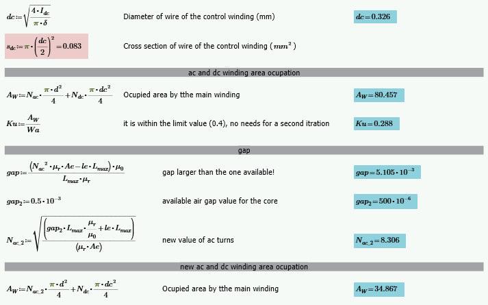
132 APPENDIX B 106 Válter de Sousa Costa


133 VARIABLE INDUCTOR DESIGN Válter de Sousa Costa 107


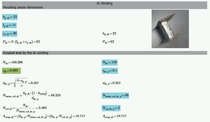

134 APPENDIX B 108 Válter de Sousa Costa


135 VARIABLE INDUCTOR DESIGN Válter de Sousa Costa 109


136 APPENDIX B LabVIEW Software Application for the VI Project and Design: The software in LabVIEW used for design the VI was previously made by another student Samuel Ferreira, during his Master Thesis [16]. 110 Válter de Sousa Costa
137 PROTOTYPE CONSTRUCTION DETAILS C. Prototype Construction Details C. Appendix C In this section of the appendix, the details of the designed PCBs are shown. The schematics and board drawings in EAGLE Light Edition Software, as well as the necessary components list, for the construction of the LLC resonant converter prototype are presented. The design of the PCBs is briefly presented below using the schematics, board drawings and the picture of the boards with and without the components. In addition, the transformer and the VI construction is shown by pictures and finally the global assembly of the converter prototype is shown. Válter de Sousa Costa 111
138 APPENDIX C Fig. C.1 Block diagram of the built prototype 112 Válter de Sousa Costa


139 PROTOTYPE CONSTRUCTION DETAILS C.1. DC Bus generator To generate the DC Bus used to feed the LLC-VI resonant converter ($ EF ) the circuit shown in Fig. C.2 a) is used. Block A corresponds to the national grid power. Block B corresponds to full-bridge rectifier and is implemented by the white box shown in the right picture. Block C corresponds to the filter capacitor and is implemented by the black capacitors in the right picture. Fig. C.2 Schematic of the DC bus generator [ref] C.2. LLC-VI Resonant Converter The LLC-VI resonant converter is composed by: half-bridge inverter, resonant filter, highfrequency transformer, and high-frequency full-bridge rectifier. The following figures present the schematics of the electrical circuits and PCB project and pictures of the build PCBs. Half-Bridge Inverter: Fig. C.3 shows the schematic for the half-bridge inverter PCB and, Fig. C.4 shows the board design, the PCB prototype top and bottom layer and, the PCB full-assembly. Válter de Sousa Costa 113


140 APPENDIX C Fig. C.3 Half-bridge inverter schematic Fig. C.4 Half-bridge inverter PCB prototype (100 x 80 mm), Board design; PCB Top and Bottom Layer and PCB full assembly The Block D in Fig. C.4 shows the half-bridge inverter schematic. The top picture in the middle shows the board design in the Eagle software. In the bottom, the pictures show the top 114 Válter de Sousa Costa
141 PROTOTYPE CONSTRUCTION DETAILS and bottom layer of the manufactured PCB. Finally, the top right picture is the PCB fullassembly. Tab. C.1 shows the components list for the PCB board. Tab. C.1 Half-bridge inverter components list Name Dimension Number of layers Observation Board Half-bridge inverter Rev x 80 mm 2 - Top + Bottom Half-bridge inverter board Schematic description Value Component Observation 1 PWR_IN 15V /-/ GND Power in +15V 2 PWR_OUT 15V /-/ GND Power out +15V 3 C15V1 100u Electrolitic capacitor 4 C15V2 0,1u Ceramic capacitor 5 R15V 1k Resistor 6 15V LED 15V 7 R_FAN 22 Resistor 8 FAN_OUT -/ 12V / GND Fan power +12V 9 IC Voltage regulator 5V 10 C5V1 100u Electrolitic capacitor 11 C5V2 0,1u Ceramic capacitor 12 R5V 1k Resistor 13 5V LED 5V 14 MOS1 +5V / GND Power for MOSFET Drivers 15 MOS2 +5V / GND Power for MOSFET Drivers 16 Input + + from DC Bus 17 Input - - from DC Bus 18 VGS1 Jumper Measure Vgs1 19 VGS2 Jumper Measure Vgs2 20 SiC Gate Driver 9A MOS1 PCB board - Driver for the Silicon Carbide Power MOSFETs 21 SiC Gate Driver 9A MOS1 PCB board - Driver for the Silicon Carbide Power MOSFETs 22 MOSFET 1 C2M MOSFET N-Channel 23 MOSFET 2 C2M MOSFET N-Channel 24 Output Output of the MOSFET arm 25 Heatsink MOS1, MOS2 3 x 63 x 55 (exp x comp x alt) 26 FAN DC 12V 0,21A Resonant Filter: Fig. C.5 shows the schematic for the resonant filter PCB and, Fig. C.6 shows the board design, the PCB prototype top and bottom layer and, the PCB full-assembly. The resonant filter PCB includes the VI and the resonant capacitor and also a buck converter to control, in close-loop operation, the DC current for controlling the inductance value of the VI. Válter de Sousa Costa 115
,")


142 APPENDIX C Fig. C.5 Resonant filter schematic Fig. C.6 Resonant filter PCB prototype 100 x 80 mm), Board design; PCB Top and Bottom Layer and PCB full assembly Block E in Fig. C.6 shows the resonant filter schematic. The top picture in the middle shows the board design in the Eagle software. In the bottom, the pictures show the top and bottom layer of the manufactured PCB. Finally, the top right picture is the PCB full-assembly. Tab. C.2 shows the components list for the PCB board. 116 Válter de Sousa Costa
143 PROTOTYPE CONSTRUCTION DETAILS Tab. C.2 Resonant filter components list Name Dimension Number of layers Observation Resonant Filter Rev x 80 mm 2 - Top + Bottom Resonant Filter board Board Schematic description Value Component Observation 1 PWR_IN 15V /-/ GND Power in +15V 2 PWR_OUT 15V /-/ GND Power out +15V 3 C15V1 100u Electrolitic capacitor 4 C15V2 100u Electrolitic capacitor 5 C15V3 0,1u Ceramic capacitor 6 R15V 1k Resistor 7 LED15V 15V 8 R_FAN 22 Resistor 9 FAN_OUT -/ 12V / GND Fan power +12V 10 IC Voltage regulator 5V 11 C5V1 100u Electrolitic capacitor 12 C5V2 0,1u Ceramic capacitor 13 C5V3 0,1u Ceramic capacitor 14 R5V 1k Resistor 15 5V LED 5V 16 DSP 6 pins (2x3) Male conector 17 R15V 470 Resistor 18 OK1 HCPL2630 Optocoupler 19 R2 100 Resistor 20 R3 100 Resistor 21 MOS1 BS108 MOSFET N-Channel 22 RZ Resistor 23 DZ Zener Diode 24 IC2 INA193 Current Shunt monitor -16V to +80V Common-Mode Range 25 C_SENS 0,1u Ceramic capacitor 26 R_SHUNT Resistor 27 MOS_BUCK IRFZ44N MOSFET N-Channel 28 D1 80SQ040 Schottky Rectifier Diode Buck Converter 29 L Inductor 30 C Ceramic Capacitor 31 IDC+ Jumper IDC from PCB or EXT 32 IDC- Jumper IDC from PCB or EXT 33 EPCOS ETD44 Variable Inductor ETD 44/22/15 ferrite core 34 VC_PP Measure VC_PP Jumper Integrator circuit used to obtain 35 IAC_PP Measure IAC_PP Jumper the values for the Lac 36 R_LAC 100k Resistor characteristic curve 37 C_LAC 2,2n Ceramic capacitor 38 CR- Holes for Cr capacitor 39 CR+ connection 40 IN Terminal block 2x5mm 41 Cr Terminal block 2x5mm 42 OUT Terminal block 2x5mm 43 FAN DC 12V 0,21A Fig. C.7 shows the VI components and assembly. Fig. C.7 b) shows the coiling machine used to make the VI coils (this machine was already existent in the laboratory and was previously built by other students for coiling the windings for VIs and transformers). Válter de Sousa Costa 117
 b) c) d) e) Fig. C.")
 VI parts; d) VI full assembly; e) Tests of the VI Fig. C.")
 and a LCR")

 curve (Small-signal characteristics), shown in Fig. C.8, was obtained for a!")
144 APPENDIX C a) b) c) d) e) Fig. C.7 VI parts, assembly and tests: a) ETD 44/22/15 ferrite core; b) Coiling machine; c) VI parts; d) VI full assembly; e) Tests of the VI Fig. C.7 e) shows a picture during the experimental tests to the VI. Using a current source YOKOGAWA GS610 Source Measure Unit (top left) and a LCR meter ISO-TECH LCR Meter LCR821 (top right) it was possible to measure the inductance values as function of the DC control current ) to characterize the VI Small-Signal Analysis. The ) curve (Small-signal characteristics), shown in Fig. C.8, was obtained for variation between 0 and 1.5A and the range obtained (measured with the LCR meter) for a frequency of 100 khz was from 5.56 ƒ to ƒ, corresponding to the maximum and minimum values respectively as in Tab. C Válter de Sousa Costa
145 PROTOTYPE CONSTRUCTION DETAILS Tab. C.3 HE ) measured [A] HE [ƒ] Lvi [uh] 10 5 Lvi [uh] 0 0 0,5 1 1,5 Idc [A] Fig. C.8 HE ) measured curved Transformer: Fig. C.9 shows the schematic for the transformer PCB and, Fig. C.10 shows the board design, the PCB prototype top and bottom layer, the PCB full-assembly and the transformer prototype during some experimental tests. Válter de Sousa Costa 119


146 APPENDIX C Fig. C.9 Transformer PCB schematic Fig. C.10 Transformer PCB prototype 100 x 80 mm), Board design; PCB Top and Bottom Layer and PCB full assembly and transformer prototype during experimental tests Block F in Fig. C.10 shows the transformer schematic. The top picture in the middle left shows the board design in the Eagle software. In the bottom, the pictures show the top and bottom layer of the manufactured PCB. The top middle picture in the right is the PCB fullassembly and finally, the left picture shows the transformer during some experimental tests. Using a LCR meter BK PRECISION Model 889B Bench LCR/ESR Meter it was possible to measure the inductance values for 5 and 6 used in the calculations for the converter design. The transformer characteristics were previously presented in Table 5..Tab. C.4 shows the components list for the PCB board. 120 Válter de Sousa Costa
147 PROTOTYPE CONSTRUCTION DETAILS Tab. C.4 Transformer PCB components list Name Dimension Number of layers Observation Board Transformer Rev x 80 mm 1 - Bottom Transformer board Schematic description Value Component Observation 1 PWR_IN 15V /-/ GND Power in +15V 2 PWR_OUT 15V /-/ GND Power out +15V 3 C15V1 100u Electrolitic capacitor 4 C15V2 100u Electrolitic capacitor 5 C15V3 0,1u Ceramic capacitor 6 R15V 1k Resistor 7 LED15V 15V 8 R_FAN 22 Resistor 9 FAN_OUT -/ 12V / GND Fan power +12V 10 Primary Terminal block 2x5mm 11 Secondary Terminal block 2x5mm 12 EPCOS ETD44 ETD 44/22/15 ferrite core 13 FAN DC 12V 0,21A Full-bridge rectifier: Fig. C.11 shows the schematic for the full-bridge rectifier PCB and, Fig. C.12 shows the board design, the PCB prototype top and bottom layer, and the PCB full-assembly. Fig. C.11 Full-bridge rectifier board schematic Válter de Sousa Costa 121


 24 Heatsink D2, D4 3 x 63 x 55 (exp x comp x alt) 122 Válter de Sousa Costa")
148 APPENDIX C 4%352-3 / Fig. C.12 High-frequency Full-Bridge rectifier PCB prototype 100 x 80 mm), Board design; PCB Top and Bottom Layer and PCB full assembly Block G in Fig. C.12 shows the high-frequency full-bridge rectifier schematic. The top picture in the middle shows the board design in the Eagle software. In the bottom, the pictures show the top and bottom layer of the manufactured PCB. Finally, the top right picture is the PCB full-assembly. Tab. C.5 shows the components list for the PCB board. Tab. C.5 Full-bridge rectifier components list Name Dimension Number of layers Observation Board Full-bridge Rectifier Rev x 80 mm 2 - Top + Bottom Full-bridge rectifier Schematic description Value Component Observation 1 PWR_IN 15V /-/ GND Power in +15V 2 PWR_OUT 15V /-/ GND Power out +15V 3 C15V1 100u Electrolitic capacitor 4 C15V2 100u Electrolitic capacitor 5 C15V3 0,1u Ceramic capacitor 6 R15V 1k Resistor 7 LED15V 15V 8 R_FAN 22 Resistor 9 FAN_OUT -/ 12V / GND Fan power +12V 10 IN Terminal block 2x5mm 11 ID1_D4 Terminal block 2x5mm 12 Co + Terminal block 2x5mm 13 Co - Terminal block 2x5mm 14 ID2_D3 Terminal block 2x5mm 15 ICo Terminal block 2x5mm 16 Io Terminal block 2x5mm 17 OUT Terminal block 2x5mm 18 D1 80EPF12 Rectifier Diode 19 D2 80EPF12 Rectifier Diode 20 D3 80EPF12 Rectifier Diode 21 D4 80EPF12 Rectifier Diode 22 FAN DC 12V 0,21A 23 Heatsink D1, D3 3 x 63 x 55 (exp x comp x alt) 24 Heatsink D2, D4 3 x 63 x 55 (exp x comp x alt) 122 Válter de Sousa Costa
 Programmable DC Electronic Load BK PRECISION 8522 2400W Block H in Fig. C.13 shows the load schematic.")

149 PROTOTYPE CONSTRUCTION DETAILS C.3. Load To emulate the load behavior two resistors were used as shown in Fig. C.13. Fig. C.13 Converter load: a) Resistive 5.6 Ω load; b) Programmable DC Electronic Load BK PRECISION W Block H in Fig. C.13 shows the load schematic. Theoretical, simulation and experimental analysis was made using a resistive load to simulate the battery behavior. The top picture in the left, shows the variable resistor used 5.6 Ω / 6A. In the bottom left, is shown a Programmable DC Electronic Load BK PRECISION W. C.4. Controller Fig. C.14 shows the block diagram of the controller used to control the switching of the SiC MOSFET switches in the half-bridge inverter. Fig. C.14 Block diagram of the controller The controller is composed by four blocks: I represents the SiC MOSFET Drivers to generate the electric signals to drive SiC MOSFET switches. J represents the Fiber Optic Emitter PCB; K represents the DSP control board; L represents a computer used to program the DSP control board; Válter de Sousa Costa 123


150 APPENDIX C SiC MOSFET Drivers: The SiC MOSFET from the half-bridge inverter are driven each one, by a fiber optic driver. The PCB board of the drivers is shown in Fig. C.15. The SiC MOSFET Drivers were already existent in the Laboratory and were used in this work because they allow controlling the SiC MOSFET switches with a frequency limited to 100 khz. Fig. C.15 Fiber optic drivers PCB, Top and Bottom view and, the assembled drivers in the halfbridge inverter PCB The SiC MOSFET Drivers are assembled in the half-bridge inverter PCB as shown in Fig. C.15 in the right. The drivers convert the electric signals from the DSP control board to optic signals to the input of the SiC MOSFET drivers. Fiber optic emitter: Fig. C.16 shows the schematic for the Fiber Optic Emitter PCB and, Fig. C.17 shows the board design, the PCB prototype top and bottom layer, the PCB full-assembly and the transformer prototype during some experimental tests. 124 Válter de Sousa Costa
, Board design; PCB")


151 PROTOTYPE CONSTRUCTION DETAILS Fig. C.16 Fiber optic emitter board schematic M ;% *L *L Fig. C.17 Fiber Optic Emitter PCB prototype 62x52 mm), Board design; PCB Top and Bottom Layer and PCB full assembly Block J in Fig. C.17 shows the Fiber Optic Emitter board schematic. The top picture in the middle shows the board design in the Eagle software. In the bottom, the pictures show the top and bottom layer of the manufactured PCB. Finally, the top right picture is the PCB fullassembly. Tab. C.6 shows the components list for the PCB board. Válter de Sousa Costa 125
152 APPENDIX C Tab. C.6 Fiber optic emitter components list Name Dimension Number of layers Observation Board Fiber Optic Emitter Rev.1 62 x 52 mm 2 - Top + Bottom 4 Channels fiber optic emitter with enable pin Schematic description Value Component Observation 1 PWR_IN 15V /-/ GND Power in +15V 2 PWR_OUT 15V /-/ GND Power out +15V 3 C15V 100u Electrolitic capacitor 4 C15V1 100u Electrolitic capacitor 5 C15V3 0,1u Ceramic capacitor 6 R15V 1k Resistor 7 LED15V 15V 8 IC Voltage regulator 5V 9 C5V2 100u Electrolitic capacitor 10 C5V1 100u Electrolitic capacitor 11 C5V 0,1u Ceramic capacitor 12 R5V 1k Resistor 13 LED5V 5V 14 R1 100 Resistor 15 R2 100 Resistor 16 R3 100 Resistor 17 R4 100 Resistor 18 CH1 HFBR1527Z Fiber Optic Transmitter 19 CH2 HFBR1527Z Fiber Optic Transmitter 20 CH3 HFBR1527Z Fiber Optic Transmitter 21 CH4 HFBR1527Z Fiber Optic Transmitter 22 JP1 header 6 pins (3x2) 23 RN1 7x470 CI resistor 24 OK1 HCPL2630 Optocoupler 25 OK2 HCPL2631 Optocoupler 26 OK3 HCPL2632 Optocoupler 27 R2_1 1k Resistor 28 R2_2 1k Resistor 29 R2_3 1k Resistor 30 R2_4 1k Resistor 31 R2_5 1k Resistor 32 IC1 CD4071 CI Logic Ports OR (4x) Before the full assembly of the half-bridge inverter some experimental tests were perform to verify the drivers and the fiber emitter board operation as shown in Fig. C Válter de Sousa Costa
 b) Fig. C.")


153 PROTOTYPE CONSTRUCTION DETAILS a) b) Fig. C.18 Fiber optic emitter and SiC MOSFET drivers experimental test prototype: a) Driver testing; b) Half-bridge inverter testing DSP Control Board: In order to control the converter, a DSP control board from Texas Instruments, shown in Fig. C.19, was used. Fig. C.19 DSP board from Texas Instruments 150 x 65 mm) The DSP control board is used to generate the electric signals to the Fiber Optic Emitter PCB to control the SiC MOSFET switching. The DSP generates two square wave electric signals with 100 khz frequency and 50% duty cycle. The signals are then used to control the switching of the SiC MOSFET switches. The SiC MOSFET drivers receive fiber optic signals. An interface board was design and built Fiber Optic Emitter. The block diagram in Matlab/Simulink used to create the PWM signal at 100 khz and 50% duty cycle is shown in Fig. C.21. Computer: In order to program the DSP control board (Fig. C.19) a computer existent in the laboratory was used. Matlab software and Matlab/Simulink library were used to build a block program for the SiC MOSFET transistors and it was compiled for C language and transfer to the DSP control board using Code Composer Studio (CCS) software shown in Fig. C.20. Válter de Sousa Costa 127

154 APPENDIX C Fig. C.20 Print screen of the computer monitor. CCS workspace left), Matlab workspace Top right) and, Matlab/Simulink block program Bottom right) Fig. C.21 Block diagram in Matlab/Simulink In order to choose the switching frequency and the dead-time of the square waves for controlling the SiC MOSFET switching, an auxiliary code in Matlab was used as shown below: %%%%%%%%%%%%%%%%%%%%%%%%%%%%%%%%%%%%%% % DSP - Controlador conversor LLC %%%%%%%%%%%%%%%%%%%%%%%%%%%%%%%%%%%%%% % Sample time Ts=1e-5; % Frequência f=100e3; % Período T=1/f; % Deadtime deadtime = 100e-9; % Percentagem de deadtime relativamente % a um período percent=(deadtime/t)*100; % Cálculos auxiliares Tdeadband = round((deadtime/t)*1023*2); 128 Válter de Sousa Costa
155 PUBLISHED ARTICLES D. Published Articles D. Appendix D This section of the appendix presents the articles published in the 51 st International Universities Power Engineering Conference (UPEC 2016, Coimbra, Portugal) entitled Analysis and Simulation of the LLC Resonant Converter under Different Control Methods and the article published in the 42 nd Annual Conference of the IEEE Industrial Electronics Society (IECON 2016, Florence, Italy) entitled Evaluation of a Variable- Inductor-Controlled LLC Resonant Converter for Battery Charging Applications. Válter de Sousa Costa 129
156
157 Analysis and Simulation of the LLC Resonant Converter under Different Control Methods Valter S. Costa 1,2, M. S. Perdigão 1,2, A. S. Mendes 1 1 Instituto de Telecomunicações, University of Coimbra, DEEC, Coimbra, 2 IPC, Instituto Superior de Engenharia de Coimbra, ISEC, DEE, Portugal, valter.costa@isec.pt, perdigao@isec.pt J. M. Alonso University of Oviedo, Electrical Eng. Dept., Tecnología Electrónica, Spain marcos@uniovi.es Abstract This paper presents the analysis and design methodology for a LLC resonant converter controlled using two different control methods, switching frequency and VI (Variable Inductor). In order to compare both control techniques a battery charger is analyzed and simulation results are presented. In order to control the converter gain, the converter is regulated in the first case by varying the switching frequency and, in the second case, is regulated through a variable resonant tank. The design methodology is presented and simulation results were obtained and compared with the theoretical ones considering a simple battery charger application. Keywords DC-DC power converters, Resonant inverters, Battery chargers I. INTRODUCTION The number of researchers reporting or analyzing the performance of the LLC resonant converter has increased drastically in recent years. A high number of applications have demonstrated that the LLC resonant converter is highly performing. From high-density dc-dc converters to mid to low power LED drivers [1],[2], or classical 48 V telecom power sources [3], the resonant mode of operation is pointed out as a main advantage for its high efficiency at the resonant frequency and its inherent capability of reducing switching losses due to ZVS (Zero Voltage Switching) characteristics. Battery chargers are also referred as benefiting from the inherent LLC characteristics. In addition, high reliability, high efficiency and low component cost can all be provided by choosing this topology [4]-[6]. This paper analysis the classical LLC converter topology controlled by the switching frequency, and controlled with a variable resonant tank, using a VI as shown in Fig. 1. Depending on the operating conditions, the paper will analyze the performance, ZVS and ZCS, full-load and no-load operation. Another explored condition is to mix both control variables, frequency and variable resonant tank in order to verify the impact on the output regulation. II. LLC RESONANT CONVERTER The proposed converter topology is based on the halfbridge inverter feeding an LLC resonant tank. The converter generally provides galvanic isolation by using an isolation transformer, which is followed by a rectifier stage. For the purpose of this work, the load will be a battery bank. Fig. 1. Proposed LLC resonant converter The typical LLC resonant converter can be divided in three modules as shown in Fig. 1 [7]. Fig. 1 presents the adopted current and voltage definitions. By turning the switches and with 50% duty cycle and complementary to each other a square voltage wave is created at the input of the resonant network. In the present case a half-bridge inverter is used, but a full-bridge inverter could also be used. Typically the resonant tank has three components: a resonant inductor,, the magnetizing inductance of the transformer, and a resonant capacitor,. In the case of the VI control, the role of the resonant inductor is done by the variable inductor, as opposed to the classical topology where the leakage inductance of the transformer is used. In the classic topology this is done to avoid using two magnetic components. In this case, adding a new magnetic device allows the converter to operate at constant switching frequency ( ) or even to use both control variables and to regulate the ouput. The goal of the resonant tank is to filter the higher harmonic currents in order to allow only the fundamental component of the current to flow through the resonant tank, even when a square wave voltage is applied to the input. A. Behaviour of the LLC Resonant Converter The LLC resonant converter is known to be capable of providing a wide output voltage range and safe-operation from no-load to short-circuit conditions [7]. When is the control variable, it is natural to operate the converter around the resonant frequency, = associated to the series elements of the resonant tank, and. Around this frequency, the gain characteristics are almost independent of /16/$ IEEE
158 the load [7]. Traditionally, the control is made by varying. The required range will be relatively small to guarantee enough controllability of the output gain (depending on the application) [7]. Therefore narrow range with light load and ZVS capability with even no load are commonly described as key benefits. It can also be seen that the gain changes with the load when is different from. The border between ZVS and ZCS operation is given by the peak gain, i.e. ZCS to the left and ZVS to the right, respectively. In case of no-load, the peak gain is maximum and it occurs when = = associated to the series-parallel elements of the resonant tank, and. Operating above the resonant tank is inductive and the input current, lags the voltage applied to the resonant tank,. The converter operates similar to a series resonant converter and therefore at the converter has only one operating point, which means no output regulation. Above, switching losses will be minimized, due to ZVS. Working near resonance has the advantage of near sinusoidal waveforms. Below and above the boundary between ZVS/ZCS, formed by the peak of the family load vs. gain curves, the converter still operates in ZVS. This will not be the case if the converter is operated below the boundary leading to a capacitive operation [8]. B. General Analysis using FHA and Design Methodology In order to use the first harmonic approximation (FHA) it is assumed that the filtering action of the resonant network is enough so that only the fundamental component of the square wave voltage contributes to the power transfer to the output. Fig. 2a) shows the AC equivalent circuit for the LLC- VI and, Fig. 2b) shows the simplified AC equivalent circuit for the LLC resonant converter [11]. If is adopted as control variable, is assumed to be zero. Fig. 2. LLC resonant converter: a) AC equivalent circuit; b) Simplified AC eqivalent circuit Following the design procedure from [11], the converter equations needed for the design using FHA are shown in TABLE I. is a ratio between and and is typically [5;10] according to [11]. From (2), a minimum voltage gain at % can be obtained as & ' ') = & * = + and, considering an allowed voltage variation at the input, a maximum gain can be obtained and depends on the input voltage and the minimum gain, &,- =. /0_2/0. /0_234 & *. Finally, Fig. 2a) may be redesigned in terms of and as shown in Fig. 2b), where an ideal transformer is included and = + // and = +. The next section will analyse the impact of the and the VI on the design methodology and converter operation. General Equations for the LLC-VI LLC control method [11] Resonant tank Mesh analysis Voltage gain M TABLE I. LLC CONVERTER EQUATIONS 1 Vin = + jωllkp + jωlvi + jωlm I1 jωlm I2 jωcr 2 = R + jωn L + jω L I jω L I ; Vo = I2 R ( ) 0 ac lks m 1 m 2 V R Vin 1 Rac + n jωl lks + jωl + jωl + jωl + 1 jωl jωcr jωlm o ac ( jω ) = = 2 Voltage 2n Vo M gain ( jω ) = = V Q Lr C r = ; m R ac 1 Cr = 2πQ f R 0 lkp in L k = ; L ac ; lkp vi m m 2 ω k 2 ω p k ω ω ( k + 1) ω j 1 Q ω0 ω0 2 k 1 ω + p R ac 1 Lr = ; L C ( 2π f ) 2 0 (2) 2 8n = R ; V N p o 2 o Ro = ; n = π I N r p 2 ( k + 1) ( 2k + 1) = L o r ; ac Vin _max n = M 2 2 ( V + V ) o F s min (1)
159 III. CONTROL VARIABLES IMPACT ON THE LLC RESONANT CONVERTER A. LLC Resonant Converter for Battery Charger Application In order to prove the design methodology presented in this paper and considering both control techniques a simple battery charger application is considered. Fig. 3 shows the battery voltage and current profiles. The voltage and current are dependent on the state-of-charge (SOC) of the battery or battery bank. For this reason, during charging, the battery voltage 789 is not constant. The converter must cope with these changes and therefore must be capable of providing a wide output voltage range and safe-operation from no-load to short-circuit conditions [7]. The LLC isolated converter is capable of dealing with these requirements, since ZVS is guaranteed in the primary side and ZCS is assured in the secondary [4]. These requirements will also be kept with the LLC-VI. Fig. 3. Battery voltage and current profiles and, behavior of and values along the charging process: (a) control and, (b) control Fig. 3a) and Fig. 3b) show the voltage and current profiles and, behavior of and considering frequency and VI control, respectively. Using the VI control method, in the charging stage the goal is to have a constant charging current, starting with an initial value for. Since the battery voltage is not constant, the controller needs to act on the inductance value to compensate the effect of the voltage variation. In this case, as the voltage increases from a minimum value, needs to decrease from _ (SOC ~0%), to maintain a constant charging current until an acceptable SOC is achieved (SOC~90% at _=). This mode is identified as current charging stage, CCS. In the next stage, identified as VCS (voltage charging stage), when the battery is almost fully charged, the voltage needs to be maintained at a constant maximum value as the charging current tends to decrease naturally to its floating level > 7_?7,9. At this point, tends to its minimum value _ (SOC 100%). During the whole process is kept constant. This simple approach is sufficient to prove the converter performance, however more complex charge control algorithms can be implemented to improve the efficiency of the application itself. Using the frequency control method, the charging profile is similar to the previous case but, in this case, the resonant inductor from Fig. 1 is not considered in the circuit and, the resonant inductor paper is done using the leakage inductance of the transformer. The control variable is. During CCS, varies from _ (SOC ~0%) to, _= (SOC ~90%), to maintain a constant charging current as the battery voltage increases. During VCS, tends to its minimum value _ (SOC 100%) maintaining the voltage at is maximum value as the charging current tends do its floating level > 7_?7,9. The simple approach presented in Fig. 3 is sufficient to prove the converter performance; however more complex charge control algorithms can be implemented to improve the efficiency of the application itself. Having a battery bank as load, inductive operation is needed, therefore the converter will operate only at or above resonance. Above resonance, ZVS operation appears but the waveforms have more distortion. B. VI Control Method Fig. 4 presents the gain curves as function of, &@ A at 10 khz and 100 khz using (1) from TABLE I. Fig. 4a) presents these curves for different load values. It is possible to observe that a higher frequency leads to a narrower voltage gain peak. The previous resonance point considered in the design methodology, for =, occurs now when is zero. At this point, the voltage gain is independent of load and frequency variation. In this case since the value of changes, so does the resonance frequency. Mathematically, resonance may occur for negative values of. Since a negative value of is not possible, it implies that the real operating region will always be a ZVS inductive region. From Fig. 4b) it can be seen that for a given voltage gain variation, &, when the frequency is FGA the variation of inductance needed to obtain that gain A is smaller when compared to a lower FGA gain curve. Therefore, for the same inductance range, a higher value of will lead to a higher controllable range of the output. Increasing enables circuit miniaturization and operating at constant facilitates the design of the EMI filter. Fig. 4. Gain curves as function of at 10 FG and 100 FG: a) &@ A at different load levels; b) &@ A at full-load This converter has inherent no-load and short-circuit protection. For short-circuit conditions, the resonant current would be limited by. For no-load, this current is equal to the magnetizing current of the transformer. Therefore, using the variable inductance concept, the converter can provide a controllable output and be operated at constant switching frequency, advantageous in EMC (electromagnetic
160 compatibility) and miniaturization issues, without compromising reliability and performance [9]. C. Switching Frequency Control Method In order to analyse the impact of the switching frequency on the LLC converter operation, the voltage gain must be obtained as a function of the switching frequency. Similar to the VI control method, (1) can be used to obtain the gain curves as function of. In this case, is not considered and is set to be zero in (1). The variation of is made by knowing that % = 2 I. Fig. 5 presents the gain curves as function of, &@ A considering a design for 10 FG and 100 FG. Fig. 5a) presents these curves for different load values. In this case unlike the previous case it is possible to observe that considering the design for a lower frequency leads to a narrower voltage gain peak. At and around resonance, the voltage gain is independent of the load and frequency variation. As the resonant filter components are constant, is always constant even with variation. Since the converter is designed initially to operate at resonance considering the maximum power in the output at this point, and that in normal operation, it will only operate at or above to regulate the output, ZVS is always guaranteed. From Fig. 5b) it can be seen that for a given voltage gain variation, &, when the design frequency is FGA the variation of needed to obtain that gain A is higher when compared to a lower frequency FGA gain curve. Therefore, for the same range, when the design is for a lower value of it will lead to a higher controllable range of the output. Nevertheless, from Fig. 5a) above resonance, if the frequency of design is higher, the operation is less load dependent although it allows less output regulation with the same variation of. Another advantage of increasing the design frequency is that enables circuit miniaturization. + + &'( '( )'( *'( '( D. Control Variables Range In order to identify the required inductance and frequency range for the application, the output power must be calculated. Using (1) and knowing that & = *. J from [7] the output. /0 converter power can be obtained as: 2 Vin 2 V 2 2 o n Po = = M ( jω ) (3) R R o 1) VI control range Considering the voltage and current profiles presented in Fig. 3a), the output power for the three levels of SOC corresponding to _, _= and, _ can be obtained by using (3). The results are shown in Fig. 6. By intersecting the gain curves of Fig. 6 with the defined power levels, _, _= and, _ are obtained. The inductance range is defined with _ and _. The procedure for the construction of the VI can be find in previous literature [9]. 2) Frequency Control Range Similar to the previous case, in order to identify the required frequency range for the application, the output power must be calculated. In this case, the output power is calculated using (3) and the gain &@K%A is also obtained using (1) where % = 2 I and, is kept at zero ( = 0). In this case, is the control variable. Considering the voltage and current profiles presented in Fig. 3b), the output power for the three levels of SOC corresponding to _, _= and, _ can be obtained using (3). The results are shown in Fig. 7. By intersecting the gain curves of Fig. 7 with the defined power levels, _, _= and, _ are obtained. The frequency range is defined with _ and _. 3) VI and Frequency Control Fig. 8 presents the gain curves as function of, &@ A considering a design for 100 FG. From Fig. 8, it can be seen that using both control methods simultaneously can be advantageous. It is possible to obtain the same gain & with a smaller value of by increasing the value. This would imply pushing the operating point from A to B or C as shown in Fig. 8. o!"#$"% '(!"#$"% Fig. 5. Gain curves as function of for 10 FG and 100 FG design: a) &@ A at different load levels; b) &@ A at full-load Fig. 6. Output power as function of of, L A for the operating points corresponding to _, _= and _
161 Fig. 7. Output power as function of of, L A for the operating points corresponding to _, _= and _ - -& & * ) &,& 1& 2/ & / 2..,.,, / 32..,.,, / 32 " & (,&, 12 &. 12/ 12 &..,. 2 & 2/ * 25 2/ ) 0 & 2 Fig. 8. Gain curves as function of for 100 FG design for three different values of at full-load (100% load),& 2 2/ 2 2 & 2/ 0 4& # 0 4& / 2 IV. SIMULATION RESULTS In order to validate the proposed topology, simulations in PSIM were carried out considering the converter parameters shown in TABLE II., which were obtained by applying the proposed methodology. The simulation results shown in Fig. 9 and Fig. 10 were obtained under open-loop control and are referred to VI and frequency control methods, respectively. TABLE II. CONVERTER PARAMETERS FOR SIMULATION Description Specification Main parameters M * =400M; =100FG; O =0.5 _* =0.8RF ; _,- =21.1RF Magnetic = 7 ; T = 1.95 devices Transformer =15.11RF ; = 3.97RF =105.75RF, 7, Load 89.42TV ; 43RV ; W 7 8.4Ω The simulation results referred to the VI control method are shown in Fig. 9 and are referred to operating points _, _= and _ (red, green and blue, respectively) obtained from Fig. 3b). Fig. 9a) and Fig. 9b) show respectively the driver signals for S1 and S2, Z and Z and the resonant filter input voltage,. Fig. 9c), Fig. 9d), Fig. 9f) and Fig. 9g) show respectively the input current,, the current in the resonant tank,, the current in the rectifier diodes, and the output current, 789. Finally, Fig. 9e) and Fig. 9h) show respectively the voltage at the VI terminals, and the output voltage, 789. During the CCS the range of the VI is [ _ ; _= ]. When charging begins, = _, > 789 = 10[ and M 789 = 84M which corresponds to its minimum value. * //* //*& //* //*) //** /// ///& /// ///) ///* 0 Fig. 9. Waveforms from simulation which represent the three points of operation correspondent to _, _= and _, in red, green and blue, respectively: (a) Z and Z ; (b) ; (c) ; (d) ; (e) ; (f) ; (g) 789 ; (h) 789 When CCS ends, = _=, > 789 = 10[ and M 789 = 112,8M (SOC 90%). The controller switches from CCS to VCS, and the battery voltage increases to its maximum value, M 789 = 116M and the charging current tends naturally to its float value. At this point, _. The converter operates always above resonance with ZVS. When the charging process begins the rectifier diodes operate in CCM (continuous conduction mode). The analysis of shows however that the converter enters in DCM (discontinuous conduction mode). When the batteries are almost fully charged the behavior of the converters tends to an open circuit and the current through the VI, _ exhibits a triangular shape waveform similar to what would be expected for the magnetizing current,. The simulation results referred to the frequency control method are shown in Fig. 10 and are referred to operating points _, _= and _ (red, green and blue, respectively) obtained from Fig. 3a). Fig. 10a) to Fig. 10c) show respectively the driver signals for S1 and S2, Z and Z, for _, _= and _ respectively. Fig. 10d) shows the resonant filter input voltage,. Fig. 10e), Fig. 10f), Fig. 10g) and Fig. 10h) show respectively the input current,, the current in the resonant tank,, the current in the rectifier diodes, and the output current, 789. Finally, Fig. 10i) shows the output voltage, 789.
162 control variable to be smaller when compared to the case of using only one control method. V. CONCLUSIONS The goal of this paper is to analyze the LLC resonant converter and compare its behavior when using either the traditional frequency control or, using a variable resonant tank through a VI. The advantages of using simultaneously both control techniques were discussed. The converter parameters are first determined considering the traditional design methodology (used for frequency control) and then, depending on the chosen control method, the output power expression is used to determine either the necessary VI or range to control the converter output. A simple charging profile was followed. A careful theoretical and simulation analysis of the converter is presented for different switching frequencies, including the analysis of the converter output power as function of both control variables. Theoretical results were confronted with simulation and a good agreement was found. In conclusion both control parameters can be used to control the output of the LLC resonant converter achieving always ZVS: using a VI while keeping constant or using while the resonant parameters are kept constant. A higher leads to converter miniaturization and the range of the VI needed to obtain a specific output regulation will be smaller. However, if is the control variable, the range is higher. A mix between both controls methods leads to an improved performance Fig. 10. Waveforms from simulation which represent the three points of operation correspondent to _, _= and _, in red, green and blue, respectively: (a) Z and Z for _ ; (b) Z and Z for _= ; (c) Z and Z for _ ; (d) ; (e) ; (f) ; (g) ; (h) 789 ; (i) 789 TABLE III. show the theoretical and simulation results considering VI and frequency control methods for the converter design parameters defined in TABLE II. As can be seen the simulation results are similar to the expected theoretical results and the results for VI control are very similar to the results for frequency control. TABLE III. THEORETICAL AND SIMULATION RESULTS Theoretical Simulation SOC M 789 > 789 L 789 M 789 > 789 L 789 [%] [RH] [khz] [V] [A] [W] [V] [A] [W] From TABLE III. the necessary range to regulate the output is about 20RF considering only VI control, 50FG considering only control and, 10RF and 20FG considering VI and control simultaneously. In conclusion, using both control techniques simultaneously allows the range of each REFERENCES [1] Y. Wang, Y. Guan, J. Huang, W. Wang and D. Xu, "A Single-Stage LED Driver Based on Interleaved Buck Boost Circuit and LLC Resonant Converter," in IEEE Journal of Emerging and Selected Topics in Power Electronics, vol. 3, no. 3, pp , Sept [2] Shuze Zhao, Jiale Xu and O. Trescases, "Burst-Mode Resonant LLC Converter for an LED Luminaire With Integrated Visible Light Communication for Smart Buildings," in IEEE Transactions on Power Electronics, vol. 29, no. 8, pp , Aug [3] R. L. Lin and C. W. Lin, "Design criteria for resonant tank of LLC DC- DC resonant converter," IECON th Annual Conference on IEEE Industrial Electronics Society, Glendale, AZ, 2010, pp doi: /IECON [4] Z. Fang, T. Cai, S. Duan and C. Chen, "Optimal Design Methodology for LLC Resonant Converter in Battery Charging Applications Based on Time-Weighted Average Efficiency," in IEEE Transactions on Power Electronics, vol. 30, no. 10, pp , Oct [5] Musavi, F.; Craciun, M.; Gautam, D.S.; Eberle, W.; Dunford, W.G., "An LLC Resonant DC DC Converter for Wide Output Voltage Range Battery Charging Applications," in Power Electronics, IEEE Transactions on, vol.28, no.12, pp , Dec [6] Shafiei, N.; Ordonez, M.; Craciun, M.; Botting, C.; Edington, M., "Burst Mode Elimination in High-Power LLC Resonant Battery Charger for Electric Vehicles," in Power Electronics, IEEE Transactions on, vol.31, no.2, pp , Feb [7] Hangseok Choi, AN-4151, Half-Bridge LLC Resonant Converter Design Using FSFR-Series Fairchild Power Switch (FPS TM ), [8] Helen Ding, AN-1160, Design of Resonant Half-Bridge Converter using IRS2795(1,2) Control IC, International Rectifier. [9] M. S. Perdigao, S. F. Ferreira, M. Martins, A. S. Mendes and J. M. Alonso, "Finite element analysis of a variable inductor for an RSCC based LED lamp driver," Industry Applications Society Annual Meeting, 2015 IEEE, Addison, TX, 2015, pp [10] C. A. Cheng, H. W. Chen, E. C. Chang, C. H. Yen and K. J. Lin, "Efficiency study for a 150W LLC resonant converter," Power Electronics and Drive Systems, PEDS International Conference on, Taipei, 2009, pp [11] Hangseok Choi, " Design Considerations for an LLC resonant Converter," Farichild Power Seminar 2007
163 Evaluation of a Variable-Inductor-Controlled LLC Resonant Converter for Battery Charging Applications Valter S. Costa 1,2, M. S. Perdigão 1,2, A. S. Mendes 1 1 Instituto de Telecomunicações, University of Coimbra, DEEC, Coimbra, 2 IPC, Instituto Superior de Engenharia de Coimbra, ISEC, DEE, Portugal, perdigao@isec.pt Abstract Based on the respective merits of the LLC resonant converter and the VI (Variable Inductor), a new battery charger topology is proposed. This paper presents a design methodology for the LLC resonant converter controlled with a VI. The output of the converter is regulated through a variable resonant tank in order to control the charging process. A smallscale prototype fed by a 50V DC input, with an IGBT based inverter working at 11.3 khz was built in order to test the proposed control method. Experimental results are presented. Keywords LLC resonant converter, variable inductor, battery charger. I. INTRODUCTION The number of researchers reporting or analyzing the performance of the LLC resonant converter has increased drastically in recent years. A high number of applications have demonstrated that the LLC resonant converter is highly performing. From high-density dc-dc converters to mid to low power LED drivers [1],[2], or classical 48 V telecom power sources [3], the resonant mode of operation is pointed out as a main advantage for its high efficiency at the resonant frequency and its inherent capability of reducing switching losses due to ZVS (Zero Voltage Switching) characteristics. Battery chargers are also referred as benefiting from the inherent LLC characteristics. Battery chargers requirements are somehow different from other applications since the converter must provide low high-frequency current ripple to maximize the battery life, a wide output voltage to cope with typical battery voltage profiles and a flexible control in order to design appropriate charging algorithms. In addition, high reliability, high efficiency and low component cost can all be provided by choosing this topology [4]-[6]. This paper is inspired in the classical LLC converter topology by exploring a new control method, based on a variable resonant tank as shown in Fig. 1. Fig. 1 presents also the adopted current and voltage definitions. Using the variable inductance concept, the converter can provide a controllable output and be operated at constant switching frequency, advantageous in EMC (electromagnetic compatibility) and miniaturization issues, without compromising reliability and performance. ZVS is guaranteed and the whole strategy is demonstrated by a simple charging concept. J. M. Alonso University of Oviedo, Electrical Eng. Dept., Tecnología Electrónica, Spain marcos@uniovi.es II. LLC RESONANT CONVERTER The proposed converter topology is based on the halfbridge inverter feeding an LLC resonant tank. The converter generally provides galvanic isolation by using an isolation transformer, which is followed by a rectifier stage. For the purpose of this work, the load will be a battery bank. Square wave generator vin S1 S2 vin vds2 is1 ilvi=ir vlvi Lvi DC Current Source vcr Cr Resonant tank Llkp Lm n:1 Llks Fig. 1. Proposed LLC resonant converter Rectifier network The typical LLC resonant converter can be divided in three modules as shown in Fig. 1 [7]. By turning the switches and with 50% duty cycle and complementary to each other a square voltage wave is created at the input of the resonant network. In the present case a half-bridge inverter is used, but a full-bridge inverter could also be used. Typically the resonant tank has three components: a resonant inductor,, the magnetizing inductance of the transformer, and a resonant capacitor,. In this case, the role of the resonant inductor is done by the variable inductor, as opposed to the classical topology where the leakage inductance of the transformer is used. In the classic topology this is done to avoid using two magnetic components. In this case, adding a new magnetic device allows the converter to operate at constant switching frequency ( ) or even to use both control variables and to regulate the ouput. The goal of the resonant tank is to filter the higher harmonic currents in order to allow only the fundamental component of the current to flow through the resonant tank, even when a square wave voltage is applied to the input. id Co iout vout Bat YWXMQMUPYPMSTWTMQOQVODSQNPP@ ᄅ RPQV@ieee UVSS
164 A. Advantages and Behaviour of the LLC Resonant Converter The LLC resonant converter is known to be capable of providing a wide output voltage range and safe-operation from no-load to short-circuit conditions [7]. When is the control variable, it is natural to operate the converter around the resonant frequency, = associated to the series elements of the resonant tank, and. Around this frequency, the gain characteristics are almost independent of the load, as seen in Fig. 2. Traditionally, the control is made by varying. The required range will be relatively small to guarantee enough controllability of the output gain (depending on the application) [7]. Therefore narrow range with light load and ZVS capability with even no load are commonly described as key benefits. It can also be seen that the gain changes with the load when is different from. The border between ZVS and ZCS operation is given by the peak gain, i.e. ZCS to the left and ZVS to the right, respectively. In case of no load, the peak gain is maximum and it occurs when = = associated to the series-parallel elements of the resonant tank, and, where is defined as the sum of the primary leakage inductance and the magnetizing inductance. Voltage gain v S2 i r fp 60% load 40% load 80% load 100% load ZCS Capacitive region Below resonance ZVS Inductive region Below resonance 20% load Boundary ZVS/ZCS v S2 i r f0 ZVS Inductive region Above resonance Switching frequency ZCS (fs < f0) ZVS (fs > f0) Fig. 2. Typical gain curves of LLC resonant converter for various loads and capacitive and inductive region waveforms It is also noticed that operating above the resonant tank is inductive and the input current, lags the voltage applied to the resonant tank,. The converter operates similar to a series resonant converter and therefore at the converter has only one operating point, which means no output regulation. Above, switching losses will be minimized, due to ZVS. Working near resonance has the advantage of near sinusoidal waveforms. Below and above the boundary between ZVS/ZCS, formed by the peak of the family load vs. gain curves, the converter still operates in ZVS. This will not be the case if the converter is operated below the boundary leading to a capacitive operation [8]. B. LLC Resonant Converter with VI Control In the present case study an LLC resonant converter with Variable Inductor (LLC-VI) control is described. The is connected in series with the transformer primary side, but the rest of the topology is kept. As response to a dc control current, the global reluctance of the magnetic core is varied, and therefore the differential inductance of the inductor is controlled. Thus, the role of the is to change the characteristics of the resonant tank in order to have a controllable output in a similar manner to the classical control. The principle of operation may be found in prior literature and will not be further addressed in this paper [9]. In this case, the will be kept constant, which benefits the converter design (EMC and control design). However, if necessary these two control variables might act together to improve the performance of the converter. Besides small size, low component cost and high reliability, charging applications have specific requirements that are directly related to the battery voltage and current profile as exemplified in Fig. 3. These characteristics are strongly dependent on the state-of-charge (SOC) of the battery or battery bank. For this reason, during charging, the battery voltage is not constant. The converter must cope with these changes and therefore must be capable of providing a wide output voltage range and safe-operation from no-load to short-circuit conditions [7]. The LLC isolated converter is capable of dealing with these requirements, since ZVS is guaranteed in the primary side and ZCS is assured in the secondary [4]. These requirements will also be kept with the LLC-VI. In the charging stage the goal is to have a constant charging current, starting with an initial value for. Since the battery voltage is not constant, the controller needs to act on the inductance value to compensate the effect of the voltage variation. In this case, as the voltage increases from a minimum value, needs to decrease from _ (SOC ~ %), to maintain a constant charging current until an acceptable SOC is achieved (SOC~ % at _9 ). This mode is identified as current charging stage, CCS. In the next stage, identified as VCS (voltage charging stage), when the battery is almost fully charged, the voltage needs to be maintained at a constant maximum value as the charging current tends to decrease naturally to its floating level _. At this point, tends to its minimum value _ (SOC %). During the whole process is kept constant. This simple approach is sufficient to prove the converter performance, however more complex charge control algorithms can be implemented to improve the efficiency of the application itself. Lvi_0 Lvi_90 Lvi_100 CCS VCS fs [Hz] vout [V] iout [A] Lvi [H] Io_float Fig. 3. Battery voltage and current profiles and, behavior of and values along the charging process Having a battery bank as load, inductive operation is needed, therefore the converter will operate only at or above resonance. Above resonance, ZVS operation appears but the waveforms have more distortion. III. ANALYSIS AND DESIGN OF THE LLC-VI In this section the analysis and design of the converter will be discussed considering the proposed VI control method. The approach will be based on the evaluation of the converter using the fundamental harmonic approximation (FHA). UVST
165 A. General Analysis using FHA and Design Methodology In order to use the first harmonic approximation (FHA) it is assumed that the filtering action of the resonant network is enough so that only the fundamental component of the square wave voltage contributes to the power transfer to the output. Fig. 4 shows the AC equivalent circuit for the LLC-VI. Resonant tank I Lvi = I 1 I 2 ~ v DS2,1 Z in L vi C r L lkp L m n 2.L lks Mesh 1 Mesh 2 R ac R ac Assuming an input voltage variation of 10% to 15%, the maximum gain can be calculated as: Vin _ max Mmax M (3) min Vin _ min In order to identify the value of (for the calculation of the resonant parameters), it is necessary to find the peak gain curves as function of and intersect them with the specified maximum gain (assuming a variable range for ). These curves for different values are shown in Fig. 6, as obtained from (2). For a selected range the voltage gain is determined and the peak gain value is identified. This is repeated for different values of. Fig. 4. AC equivalent circuit for LLC resonant converter Considering the transformer turns ratio =, the rectifier and the load, an equivalent resistance is defined that includes the effect of the output rectifier and load resistance: 2 8n Rac R (1) 2 o where = / is the load resistance (that represents the battery bank). The design methodology starts by determining the resonant tank parameters (, and ) assuming the traditional FHA method followed by [11], considering the nominal operating point as reference. The following condition is considered at the nominal operating point: =. As previously mentioned, the LLC converter has two resonant frequencies: = determined by and and =, determined by and, where = and = + //. In a transformer, if the secondary side winding is open or short-circuited, and can be measured, respectively. Following the procedure presented in [11] and assuming that = the voltage gain for this converter can be expressed as: M 2 k 2 2nV p k 1 o j 2 2 V 2 in k 1 j 1 Q k 1 p Where = and = and is typically [ ; ] according to [11]. With this simplification, a minimum voltage gain at can be obtained as 0 = = +. Finally, Fig. 4 may be redesigned in terms of and as shown in Fig. 5, where an ideal transformer is included and = + // and = +. ~ ILvi VDS2,1 Zin Lr Lp - Lr Cr Ideal transformer 1: k+1 k Rac Rac Fig. 5. Simplified AC eqivalent circuit for LLC resonant converter (2) Fig. 6. Peak gain (maximum attainable gain) versus for different values The final value of is obtained from the intersection of the maximum gain, considering a margin of 10% ( =. ), and the peak gain curve for the selected as shown in Fig. 6. Knowing the value of, considering and, the resonant parameters can be calculated as: 1 Cr (4) 2 Q f0 Rac 1 Lr (5) 2 f C L p k 1 2k 1 r L Considering an output voltage ripple of 1%, the output capacitor can be calculated as: Io Co (7) Vripple 2 fs Finally, the transformer turns ratio is determined. Considering the diode rectifier voltage drop, the transformer turns ratio can be determined as: Np Vin _max n Mmin N s 2 Vo 2 VF (8) The next section will analyse the impact of the VI on the design methodology and converter operation. B. VI Control Impact on the Design Methodology In order to analyse the impact of the VI on the LLC converter operation, the voltage gain must be obtained as a function of this new control parameter. Applying Kirchhoff s Laws to mesh 1 and mesh 2, referred previously in Fig. 4, (9) and (10) can be written. Considering the output voltage =, and the two mesh equations, the voltage gain is obtained as in (11). r (6) UVSU
166 M 1 Vin j Llkp j Lvi j Lm I1 j Lm I2 (9) j Cr 2 R j n L j L I j L I (10) 0 ac lks m 1 m 2 V R Vin 1 Rac n j L lks j L j L j L 1 j L j Cr j Lm o ac j 2 Fig. 7 presents the gain curves as function of, at khz and khz. Fig. 7a) presents these curves for different load values. It is possible to observe that a higher frequency leads to a narrower voltage gain peak. The previous resonance point considered in the design methodology, for =, occurs now when is zero. At this point, the voltage gain is independent of load and frequency variation. In this case since the value of changes, so does the resonance frequency. Mathematically, resonance may occur for negative values of. Since a negative value of is not possible, it implies that the real operating region will always be a ZVS inductive region. From Fig. 7b) it can be seen that for a given voltage gain variation,, when the frequency is higher the variation of inductance needed to obtain that gain variation is smaller when compared to a lower frequency gain curve. Therefore, for the same inductance range, a higher value of will lead to a higher controllable range of the output. Increasing enables circuit miniaturization and operating at constant facilitates the design of the EMI filter. lkp vi m m 2 (11) Vin 2 V 2 2 o n Po M j (12) R R o For the LLC battery charger and considering the voltage and current profiles presented in Fig. 3, the output power for the three levels of SOC corresponding to _, _9 and, _ can be obtained by using (12). The results are shown in Fig. 8. Output Power [W] o Po à Lvi_90à SOC à 90% Po à Lvi_100 à SOC à100% Po à Lvi_0 à Vout_min à SOCini Voltage gain Lvi = 0 fs = constant Non operating range (Lvi < 0) ΔLvi à 100kHz ΔLvi à 10kHz Voltage gain Lvi = 0 ΔM VI inductance, Lvi [H] ZVS Indutive region Lvi inductance [H] M(Lvi) à 10kHz M(Lvi) à 100kHz 20% load 40% load 60% load 80% load 100% load 100kHz 10kHz (a) 100% load 100kHz 10kHz Fig. 7. Gain curves as function of at and : a) at different load levels; b) at full-load However, this converter has inherent no-load and shortcircuit protection. For short-circuit conditions, the resonant current would be limited by. For no-load, this current is equal to the magnetizing current of the transformer. C. VI Control Range In order to identify the required inductance range for the application, the output power must be calculated. Using (11) and knowing that = from [7] the output converter power can be obtained as: (b) Lvi inductance [H] Fig. 8. Output power as function of of, for the operating points corresponding to _, _9 and _ By intersecting the gain curves of Fig. 8 with the defined power levels, _, _9 and, _ are obtained. The inductance range is defined with _ and _. The procedure for the construction of the VI can be find in previous literature [9]. IV. SIMULATION RESULTS In order to validate the proposed topology, simulations in PSIM were carried out considering the converter parameters shown in Table I, which were obtained by applying the proposed methodology. The simulation results shown in Fig. 9 were obtained under open-loop control. TABLE I. Description Main parameters Magnetic devices,, Load Transformer CONVERTER PARAMETERS FOR SIMULATION Specification = ; = ; =. _ =. ; _ =. = ; =. =. ; =. =.. ; ;. Ω The simulation results are referred to operating points _, _9 and _ (red, green and blue, respectively) obtained from Fig. 3. Fig. 9a) and Fig. 9b) show respectively the driver signals for S1 and S2, and and the resonant filter input voltage,. Fig. 9c), Fig. 9d), Fig. 9f) and Fig. 9g) show respectively the input current,, the current in the resonant tank,, the current in the rectifier diodes, and the output current,. Finally, Fig. 9e) and Fig. 9h) show UVSV
167 respectively the voltage at the VI terminals, and the output voltage, vgs1 vds2 vgs2 is1_0 is1_90 is1_100 ilvi_0 vlvi_0 vlvi_90 vlvi_100 id_0 iout_0 ilvi_90 id_90 iout_90 Iout_0 Iout_90 Iout_100 ilvi_100 id_100 DCM iout_100 Iout range vout_0 vout_90 vout_100 Vout_100 Vout_90 Vout range MOSFET drive voltage Resonant filter voltage Input current VI current VI voltage Rectifier diodes current DCM Output current Output voltage 90 Vout_0 t1 t2 t3 t4t Time (s) ZVS_90 ZVS_0 ZVS_100 T s/2 T s T s/2 Fig. 9. Waveforms from simulation which represent the three points of operation correspondent to _, _9 and _, in red, green and blue, respectively: (a) and ; (b) ; (c) ; (d) ; (e) ; (f) ; (g) ; (h) During the CCS the range of the VI is [ _ ; _9 ]. When charging begins, = _, = and = which corresponds to its minimum value. When CCS ends, = _9, = and =, (SOC %). The controller switches from CCS to VCS, and the battery voltage increases to its maximum value, = and the charging current tends naturally to its float value. At this point, _. The converter operates always above resonance with ZVS. When the charging process begins the rectifier diodes operate in CCM (continuous conduction mode). The analysis of shows however that the converter enters in DCM (discontinuous conduction mode). When the batteries are almost fully charged the behavior of the converters tends to an open circuit and the current through the VI, _ exhibits a triangular shape waveform similar to what would be expected for the magnetizing current,. Table II shows the theoretical and simulation results for the converter design parameters defined in Table I. As can be seen the simulation results are similar to the expected theoretical results. (a) (b) (c) (d) (e) (f) (g) (h) SOC [%] TABLE II. Theoretical THEORETICAL AND SIMULATION RESULTS Simulation [W] [ H] [V] [A] [W] [V] [A] V. SMALL-SCALE LLC CONVERTER TEST RESULTS In order to validate the proposed topology an experimental small-scale prototype was built using a half-bridge IGBT based inverter. The results were obtained without closed-loop control. The converter input was fed by a DC voltage source (YOKOGAWA GS610) at constant. To simulate the load a Programmable DC Electronic Load was used (BK PRECISION W). The system specifications and converter parameters are shown in Table III. The purpose was to verify experimentally the ability to control the output of the LLC-VI. The design methodology was followed but only two operating points were considered. TABLE III. CONVERTER PARAMETERS FOR SIMULATION AND EXPERIMENTAL PROTOTYPE Description Specification Main parameters = ; =. ; =. and SEMiX202GB066HDs ; ; ; Ω,, and 80EPF12 ; =, ; ; Theoretical design _ = ; _ = Magnetic devices Transformer = ; = =. ; =. =,, Load. ; ; =. Ω Simulation and experimental parameters =.. = ; = Magnetic devices ETD44/22/15 core ;. gap = ; = ; = Transformer =, ; =, =,, Load ; ; =. Ω The obtained simulation and experimental waveforms presented in Fig. 10 and Fig. 11, show the operation of the converter at the two VI prototype limits, and. For this test the load was kept constant. Fig. 10 shows and, for and. Between these two limits the converter operates at ZVS. Fig. 11 shows,, and, for and. It can be seen that by adjusting the VI control current and regulating the inductance value it is possible to control the converter output. In Fig. 11e) the converter operates in DCM (when = the rectifier diodes are not conducting), and in Fig. 11f) operates in CCM. For the converter operates closer to resonance since the is closer to a sinusoidal. Table IV shows the theoretical, simulation and experimental results for the small-scale prototype. As expected the simulation results are very close to the theoretical results. The experimental values exhibit some variation essentially due to coupling losses in the power transformer and due to the prototype efficiency. For current and voltage values the error between the experimental and simulation results is around % and %, respectively. Nevertheless at this point, it was only intended to prove the capability of this topology regarding output regulation. UVSW
 and (c) for ; (b) and (d) for, simulation and experimental tests, respectively.")
168 p ッキ キキキ N エ ー ヲ N ッイァ I 60 VDS ILvi Time (s) (a) vds2 ilvi (c) 60 VDS ILvi Time (s) (b) Fig. 10. and,, red and blue respectively: (a) and (c) for ; (b) and (d) for, simulation and experimental tests, respectively. Experimental results, 25V/div, 0,5A/div, 25us/div Vin ILvi Vout Iout (a) Time (s) vin vout iout ilvi (c) (e) Vin ILvi vds2 vin vout Vout iout ilvi Iout ilvi (d) (b) Time (s) Fig. 11., (red and blue, respectively), and (red and blue, respectively): (a), (c) and (e) for and (b), (d) and (f) for. Experimental results and, 10V/div, 2.5V/div, respectively. and, 0.5A/div, 0.5A/div respectively, 25us/div VI prototype range TABLE IV. Theoretical results CONVERTER PARAMETERS FOR SIMULATION AND EXPERIMENTAL PROTOTYPE Simulation Results (d) (f) Experimental Results [ H] [W] [V] [A] [W] [V] [A] [W] VI. CONCLUSIONS This paper proposes an LLC resonant converter for battery charging with VI control. Two main goals were identified: the first was to explore the possibility to regulate the LLC converter output with a variable resonant tank and the second one, to apply this control technique to a battery charger. It was demonstrated that a variable inductance based LLC converter provides output power regulation and allows controlling the charging process. Taking as reference the traditional design methodology (used for frequency control) it was possible to determine the converter parameters and the required inductance range. A simple charging profile was followed, during CCS a constant output current was maintained while the increases (with increasing SOC) and, during VCS, tends naturally to its float value as reaches its maximum value. In this case the inductance is used to keep a constant output voltage (as SOC reaches its maximum). A careful analysis of the methodology is presented for different switching frequencies, including the analysis of the converter output power as function of the control variable. Theoretical results were confronted with simulation and a good agreement was found. The experimental tests of the small-scale LLC-VI allowed verifying the proposed approach. Experimental waveforms are very close to the simulation ones. An output range of variation from % to % was obtained at constant frequency. In this case, a relatively small output regulation was obtained, due to poor coupling in the transformer and efficiency losses in the converter. This is the main reason why there is some distance between the experimental values (in terms of voltage and current levels) and the simulation ones. If increases, the converter will be miniaturized and the range of the VI needed to obtain a specific output regulation will be smaller. A proper design of the magnetic components and the converter parameters (seeking efficiency) will lead to the expected values (according to the design methodology). In conclusion, the VI can be used to control the output of the LLC resonant converter achieving always ZVS while is kept constant. REFERENCES [1] Y. Wang, Y. Guan, J. Huang, W. Wang and D. Xu, "A Single-Stage LED Driver Based on Interleaved Buck Boost Circuit and LLC Resonant Converter," in IEEE Journal of Emerging and Selected Topics in Power Electronics, vol. 3, no. 3, pp , Sept [2] Shuze Zhao, Jiale Xu and O. Trescases, "Burst-Mode Resonant LLC Converter for an LED Luminaire With Integrated Visible Light Communication for Smart Buildings," in IEEE Transactions on Power Electronics, vol. 29, no. 8, pp , Aug [3] R. L. Lin and C. W. Lin, "Design criteria for resonant tank of LLC DC- DC resonant converter," IECON th Annual Conference on IEEE Industrial Electronics Society, Glendale, AZ, 2010, pp doi: /IECON [4] Z. Fang, T. Cai, S. Duan and C. Chen, "Optimal Design Methodology for LLC Resonant Converter in Battery Charging Applications Based on Time-Weighted Average Efficiency," in IEEE Transactions on Power Electronics, vol. 30, no. 10, pp , Oct [5] Musavi, F.; Craciun, M.; Gautam, D.S.; Eberle, W.; Dunford, W.G., "An LLC Resonant DC DC Converter for Wide Output Voltage Range Battery Charging Applications," in Power Electronics, IEEE Transactions on, vol.28, no.12, pp , Dec [6] Shafiei, N.; Ordonez, M.; Craciun, M.; Botting, C.; Edington, M., "Burst Mode Elimination in High-Power LLC Resonant Battery Charger for Electric Vehicles," in Power Electronics, IEEE Transactions on, vol.31, no.2, pp , Feb [7] Hangseok Choi, AN-4151, Half-Bridge LLC Resonant Converter Design Using FSFR-Series Fairchild Power Switch (FPS TM ), [8] Helen Ding, AN-1160, Design of Resonant Half-Bridge Converter using IRS2795(1,2) Control IC, International Rectifier. [9] M. S. Perdigao, S. F. Ferreira, M. Martins, A. S. Mendes and J. M. Alonso, "Finite element analysis of a variable inductor for an RSCC based LED lamp driver," Industry Applications Society Annual Meeting, 2015 IEEE, Addison, TX, 2015, pp [10] C. A. Cheng, H. W. Chen, E. C. Chang, C. H. Yen and K. J. Lin, "Efficiency study for a 150W LLC resonant converter," Power Electronics and Drive Systems, PEDS International Conference on, Taipei, 2009, pp [11] Hangseok Choi, " Design Considerations for an LLC resonant Converter," Farichild Power Seminar 2007 UVSX
TABLE OF CONTENTS CHAPTER NO. TITLE PAGE NO. LIST OF TABLES LIST OF FIGURES LIST OF SYMBOLS AND ABBREVIATIONS
 vii TABLE OF CONTENTS CHAPTER NO. TITLE PAGE NO. ABSTRACT LIST OF TABLES LIST OF FIGURES LIST OF SYMBOLS AND ABBREVIATIONS iii xii xiii xxi 1 INTRODUCTION 1 1.1 GENERAL 1 1.2 LITERATURE SURVEY 1 1.3 OBJECTIVES
CHAPTER 2 A SERIES PARALLEL RESONANT CONVERTER WITH OPEN LOOP CONTROL
 14 CHAPTER 2 A SERIES PARALLEL RESONANT CONVERTER WITH OPEN LOOP CONTROL 2.1 INTRODUCTION Power electronics devices have many advantages over the traditional power devices in many aspects such as converting
Fundamentals of Power Electronics
 Fundamentals of Power Electronics SECOND EDITION Robert W. Erickson Dragan Maksimovic University of Colorado Boulder, Colorado Preface 1 Introduction 1 1.1 Introduction to Power Processing 1 1.2 Several
An efficient switched-mode power supply using a quadratic boost converter and a new topology of two-switch forward converter
 Fernando Lessa Tofoli, Carlos Alberto Gallo e Evandro Aparecido Soares An efficient switched-mode power supply using a quadratic boost converter and a new topology of two-switch forward converter Fernando
LLC Resonant Converter for Battery Charging Application
 International Journal of Electrical Engineering. ISSN 0974-2158 Volume 8, Number 4 (2015), pp. 379-388 International Research Publication House http://www.irphouse.com LLC Resonant Converter for Battery
CONTENTS. Chapter 1. Introduction to Power Conversion 1. Basso_FM.qxd 11/20/07 8:39 PM Page v. Foreword xiii Preface xv Nomenclature
 Basso_FM.qxd 11/20/07 8:39 PM Page v Foreword xiii Preface xv Nomenclature xvii Chapter 1. Introduction to Power Conversion 1 1.1. Do You Really Need to Simulate? / 1 1.2. What You Will Find in the Following
Recent Approaches to Develop High Frequency Power Converters
 The 1 st Symposium on SPC (S 2 PC) 17/1/214 Recent Approaches to Develop High Frequency Power Converters Location Fireworks Much snow Tokyo Nagaoka University of Technology, Japan Prof. Jun-ichi Itoh Dr.
TABLE OF CONTENTS CHAPTER NO. TITLE PAGE NO. LIST OF TABLES LIST OF FIGURES LIST OF SYMBOLS AND ABBREVIATIONS
 vi TABLE OF CONTENTS CHAPTER NO. TITLE PAGE NO. ABSTRACT LIST OF TABLES LIST OF FIGURES LIST OF SYMBOLS AND ABBREVIATIONS iii x xi xvii 1 INTRODUCTION 1 1.1 INTRODUCTION 1 1.2 BACKGROUND 2 1.2.1 Types
A Double ZVS-PWM Active-Clamping Forward Converter: Analysis, Design, and Experimentation
 IEEE TRANSACTIONS ON POWER ELECTRONICS, VOL. 16, NO. 6, NOVEMBER 2001 745 A Double ZVS-PWM Active-Clamping Forward Converter: Analysis, Design, and Experimentation René Torrico-Bascopé, Member, IEEE, and
CHAPTER 4 DESIGN OF CUK CONVERTER-BASED MPPT SYSTEM WITH VARIOUS CONTROL METHODS
 68 CHAPTER 4 DESIGN OF CUK CONVERTER-BASED MPPT SYSTEM WITH VARIOUS CONTROL METHODS 4.1 INTRODUCTION The main objective of this research work is to implement and compare four control methods, i.e., PWM
CHAPTER 6 BRIDGELESS PFC CUK CONVERTER FED PMBLDC MOTOR
 105 CHAPTER 6 BRIDGELESS PFC CUK CONVERTER FED PMBLDC MOTOR 6.1 GENERAL The line current drawn by the conventional diode rectifier filter capacitor is peaked pulse current. This results in utility line
Three Phase PFC and Harmonic Mitigation Using Buck Boost Converter Topology
 Three Phase PFC and Harmonic Mitigation Using Buck Boost Converter Topology Riya Philip 1, Reshmi V 2 Department of Electrical and Electronics, Amal Jyothi College of Engineering, Koovapally, India 1,
Level-2 On-board 3.3kW EV Battery Charging System
 Level-2 On-board 3.3kW EV Battery Charging System Is your battery charger design performing at optimal efficiency? Datsen Davies Tharakan SYNOPSYS Inc. Contents Introduction... 2 EV Battery Charger Design...
A Color LED Driver Implemented by the Active Clamp Forward Converter
 A Color LED Driver Implemented by the Active Clamp Forward Converter C. H. Chang, H. L. Cheng, C. A. Cheng, E. C. Chang * Power Electronics Laboratory, Department of Electrical Engineering I-Shou University,
SHUNT ACTIVE POWER FILTER
 75 CHAPTER 4 SHUNT ACTIVE POWER FILTER Abstract A synchronous logic based Phase angle control method pulse width modulation (PWM) algorithm is proposed for three phase Shunt Active Power Filter (SAPF)
Chapter 6 Soft-Switching dc-dc Converters Outlines
 Chapter 6 Soft-Switching dc-dc Converters Outlines Classification of soft-switching resonant converters Advantages and disadvantages of ZCS and ZVS Zero-current switching topologies The resonant switch
Analysis and Design of Soft Switched DC-DC Converters for Battery Charging Application
 ISSN (Online) : 239-8753 ISSN (Print) : 2347-67 International Journal of Innovative Research in Science, Engineering and Technology Volume 3, Special Issue 3, March 24 24 International Conference on Innovations
Australian Journal of Basic and Applied Sciences. Design of a Half Bridge AC AC Series Resonant Converter for Domestic Application
 ISSN:1991-8178 Australian Journal of Basic and Applied Sciences Journal home page: www.ajbasweb.com Design of a Half Bridge AC AC Series Resonant Converter for Domestic Application K. Prabu and A.Ruby
Design and Simulation of PFC Circuit for AC/DC Converter Based on PWM Boost Regulator
 International Journal of Automation and Power Engineering, 2012, 1: 124-128 - 124 - Published Online August 2012 www.ijape.org Design and Simulation of PFC Circuit for AC/DC Converter Based on PWM Boost
A Bidirectional DC-DC High Frequency Dual-Half Bridge Series Resonant Converter: Design, Simulation and Experimental Results
 A Bidirectional DC-DC High Frequency Dual-Half Bridge Series Resonant Converter: Design, Simulation and Experimental Results by Nikhilkumar Sachdev B.Eng., Gujarat Technological University, 2012 A Project
An Interleaved Flyback Inverter for Residential Photovoltaic Applications
 An Interleaved Flyback Inverter for Residential Photovoltaic Applications Bunyamin Tamyurek and Bilgehan Kirimer ESKISEHIR OSMANGAZI UNIVERSITY Electrical and Electronics Engineering Department Eskisehir,
2015 International Future Energy Challenge Topic B: Battery Energy Storage with an Inverter That Mimics Synchronous Generators. Qualification Report
 2015 International Future Energy Challenge Topic B: Battery Energy Storage with an Inverter That Mimics Synchronous Generators Qualification Report Team members: Sabahudin Lalic, David Hooper, Nerian Kulla,
A Novel Single-Stage Push Pull Electronic Ballast With High Input Power Factor
 770 IEEE TRANSACTIONS ON INDUSTRIAL ELECTRONICS, VOL. 48, NO. 4, AUGUST 2001 A Novel Single-Stage Push Pull Electronic Ballast With High Input Power Factor Chang-Shiarn Lin, Member, IEEE, and Chern-Lin
A New Concept of Power Quality Monitoring
 A New Concept of Power Quality Monitoring Victor Anunciada 1, Hugo Ribeiro 2 1 Instituto de Telecomunicações, Instituto Superior Técnico, Lisboa, Portugal, avaa@lx.it.pt 2 Instituto de Telecomunicações,
CHAPTER 2 AN ANALYSIS OF LC COUPLED SOFT SWITCHING TECHNIQUE FOR IBC OPERATED IN LOWER DUTY CYCLE
 40 CHAPTER 2 AN ANALYSIS OF LC COUPLED SOFT SWITCHING TECHNIQUE FOR IBC OPERATED IN LOWER DUTY CYCLE 2.1 INTRODUCTION Interleaving technique in the boost converter effectively reduces the ripple current
1. The current-doubler rectifier can be used to double the load capability of isolated dc dc converters with bipolar secondaryside
 Highlights of the Chapter 4 1. The current-doubler rectifier can be used to double the load capability of isolated dc dc converters with bipolar secondaryside voltage. Some industry-generated papers recommend
466 IEEE TRANSACTIONS ON POWER ELECTRONICS, VOL. 13, NO. 3, MAY A Single-Switch Flyback-Current-Fed DC DC Converter
 466 IEEE TRANSACTIONS ON POWER ELECTRONICS, VOL. 13, NO. 3, MAY 1998 A Single-Switch Flyback-Current-Fed DC DC Converter Peter Mantovanelli Barbosa, Member, IEEE, and Ivo Barbi, Senior Member, IEEE Abstract
An electronic ballast to control an induction lamp
 An electronic ballast to control an induction lamp João F. S. Moreira, Nº68256, Instituto Superior Técnico Taguspark Abstract - The use of electromagnetic induction lamps without electrodes has increased
Máquina de Soldagem de 2kW Utilizando o Conversor Ponte Completa
 Resumo: Máquina de Soldagem de 2kW Utilizando o Conversor Ponte Completa Alexandre José Araújo dos Santos Faculdade de Tecnologia SENAI Sérgio Vidal Garcia Oliveira Universidade Regional de Blumenau Adriano
EMBEDDED CONTROLLED ZVS DC-DC CONVERTER FOR ELECTROLYZER APPLICATION
 International Journal on Intelligent Electronic Systems, Vol. 5, No.1, January 2011 6 Abstract EMBEDDED CONTROLLED ZVS DC-DC CONVERTER FOR ELECTROLYZER APPLICATION Samuel Rajesh Babu R. 1, Henry Joseph
A NEW DESIGN METHOD OF OUTPUT FILTER FOR SPACE VECTOR PWM FED INDUCTION MOTOR
 A NEW DESIGN METHOD OF OUTPUT FILTER FOR SPACE VECTOR PWM FED INDUCTION MOTOR Dr. Majid K. Al-Khatat *, Ola Hussian, Fadhil A. Hassan Electrical and Electronic Engineering Department, University of Technology
IN THE high power isolated dc/dc applications, full bridge
 354 IEEE TRANSACTIONS ON POWER ELECTRONICS, VOL. 21, NO. 2, MARCH 2006 A Novel Zero-Current-Transition Full Bridge DC/DC Converter Junming Zhang, Xiaogao Xie, Xinke Wu, Guoliang Wu, and Zhaoming Qian,
IGBT based Multiport Bidirectional DC-DC Converter with Renewable Energy Source
 IGBT based Multiport Bidirectional DC-DC Converter with Renewable Energy Source S.Gautham Final Year, UG student, Department of Electrical and Electronics Engineering, P. B. College of Engineering, Chennai
Self-oscillating Auxiliary Medium Open Loop Power Supply Deploying Boost EIE Converter
 Self-oscillating Auxiliary Medium Open Loop Power Supply Deploying Boost EIE Converter L.C. Gomes de Freitas; F.R.S. Vincenzi; E.A.A. Coelho; J.B. Vieira Jr. and L.C. de Freitas Faculty of Electrical Engineering
Generalized Multilevel Current-Source PWM Inverter with No-Isolated Switching Devices
 Generalized Multilevel Current-Source PWM Inverter with No-Isolated Switching Devices Suroso* (Nagaoka University of Technology), and Toshihiko Noguchi (Shizuoka University) Abstract The paper proposes
Simulation and Comparision of Back To Back System using Bidirectional Isolated DC-DC Converter with Active Energy Storage
 International Journal of Electrical Engineering. ISSN 0974-2158 Volume 5, Number 3 (2012), pp. 231-238 International Research Publication House http://www.irphouse.com Simulation and Comparision of Back
Multiple Output Converter Based On Modified Dickson Charge PumpVoltage Multiplier
 Multiple Output Converter Based On Modified Dickson Charge PumpVoltage Multiplier Thasleena Mariyam P 1, Eldhose K.A 2, Prof. Thomas P Rajan 3, Rani Thomas 4 1,2 Post Graduate student, Dept. of EEE,Mar
BIDIRECTIONAL CURRENT-FED FLYBACK-PUSH-PULL DC-DC CONVERTER
 BIDIRECTIONAL CURRENT-FED FLYBACK-PUSH-PULL DC-DC CONVERTER Eduardo Valmir de Souza and Ivo Barbi Power Electronics Institute - INEP Federal University of Santa Catarina - UFSC www.inep.ufsc.br eduardovs@inep.ufsc.br,
CHAPTER 3 DC-DC CONVERTER TOPOLOGIES
 47 CHAPTER 3 DC-DC CONVERTER TOPOLOGIES 3.1 INTRODUCTION In recent decades, much research efforts are directed towards finding an isolated DC-DC converter with high volumetric power density, low electro
A NEW SINGLE STAGE THREE LEVEL ISOLATED PFC CONVERTER FOR LOW POWER APPLICATIONS
 A NEW SINGLE STAGE THREE LEVEL ISOLATED PFC CONVERTER FOR LOW POWER APPLICATIONS S.R.Venupriya 1, Nithyananthan.K 2, Ranjidharan.G 3, Santhosh.M 4,Sathiyadevan.A 5 1 Assistant professor, 2,3,4,5 Students
Interleaved Current-Fed Resonant Converter with High Current Side Filter for EV and HEV Applications
 IJSTE - International Journal of Science Technology & Engineering Volume 2 Issue 10 April 2016 ISSN (online): 2349-784X Interleaved Current-Fed Resonant Converter with High Current Side Filter for EV and
A HIGH POWER FACTOR SYMMETRICAL SWITCHED-MODE POWER SUPPLY
 A HIGH POWER FACTOR SYMMETRICAL SWITCHED-MODE POWER SUPPLY Fernando Lessa Tofoli Universidade Federal de Uberlândia fernandolessa@pop.com.br Carlos Alberto Gallo Universidade Federal de Uberlândia gallo@eel.ufu.br
POWER FACTOR CORRECTION AND HARMONIC CURRENT REDUCTION IN DUAL FEEDBACK PWM CONTROLLED AC/DC DRIVES.
 POWER FACTOR CORRECTION AND HARMONIC CURRENT REDUCTION IN DUAL FEEDBACK PWM CONTROLLED AC/DC DRIVES. 1 RAJENDRA PANDAY, 2 C.VEERESH,ANIL KUMAR CHAUDHARY 1, 2 Mandsaur Institute of Techno;ogy,Mandsaur,
Improved Battery Charger Circuit Utilizing Reduced DC-link Capacitors
 Improved Battery Charger Circuit Utilizing Reduced DC-link Capacitors Vencislav Valchev 1, Plamen Yankov 1, Orlin Stanchev 1 1 Department of Electronics and Microelectronics, Technical University of Varna,
CHAPTER 2 DESIGN AND MODELING OF POSITIVE BUCK BOOST CONVERTER WITH CASCADED BUCK BOOST CONVERTER
 17 CHAPTER 2 DESIGN AND MODELING OF POSITIVE BUCK BOOST CONVERTER WITH CASCADED BUCK BOOST CONVERTER 2.1 GENERAL Designing an efficient DC to DC buck-boost converter is very much important for many real-time
PI Controller Based New Soft-Switching Boost Converter With A Coupled Inductor
 PI Controller Based New Soft-Switching Boost Converter With A Coupled Inductor 1 Amala Asokan 1 PG Scholar (Electrical and Electronics Engineering) Nehru College of Engineering and Research Centre Thrissur,
Sepic Topology Based High Step-Up Step down Soft Switching Bidirectional DC-DC Converter for Energy Storage Applications
 IOSR Journal of Electrical and Electronics Engineering (IOSR-JEEE) e-issn: 2278-1676,p-ISSN: 2320-3331, Volume 12, Issue 3 Ver. IV (May June 2017), PP 68-76 www.iosrjournals.org Sepic Topology Based High
DUAL BRIDGE LLC RESONANT CONVERTER WITH FREQUENCY ADAPTIVE PHASE-SHIFT MODULATION CONTROL FOR WIDE VOLTAGE GAIN RANGE
 DUAL BRIDGE LLC RESONANT CONVERTER WITH FREQUENCY ADAPTIVE PHASE-SHIFT MODULATION CONTROL FOR WIDE VOLTAGE GAIN RANGE S M SHOWYBUL ISLAM SHAKIB ELECTRICAL ENGINEERING UNIVERSITI OF MALAYA KUALA LUMPUR,
Single-Stage Power Electronic Converters with Combined Voltage Step-Up/Step-Down Capability
 Western University Scholarship@Western Electronic Thesis and Dissertation Repository January 2013 Single-Stage Power Electronic Converters with Combined Voltage Step-Up/Step-Down Capability Navid Golbon
THE converter usually employed for single-phase power
 82 IEEE TRANSACTIONS ON INDUSTRIAL ELECTRONICS, VOL. 46, NO. 1, FEBRUARY 1999 A New ZVS Semiresonant High Power Factor Rectifier with Reduced Conduction Losses Alexandre Ferrari de Souza, Member, IEEE,
DESIGN, SIMULATION AND IMPLEMENTATION OF A HIGH STEP-UP Z-SOURCE DC-DC CONVERTER WITH FLYBACK AND VOLTAGE MULTIPLIER. A Thesis ARASH TORKAN
 DESIGN, SIMULATION AND IMPLEMENTATION OF A HIGH STEP-UP Z-SOURCE DC-DC CONVERTER WITH FLYBACK AND VOLTAGE MULTIPLIER A Thesis by ARASH TORKAN Submitted to the Office of Graduate and Professional Studies
PIEZOELECTRIC TRANSFORMER FOR INTEGRATED MOSFET AND IGBT GATE DRIVER
 1 PIEZOELECTRIC TRANSFORMER FOR INTEGRATED MOSFET AND IGBT GATE DRIVER Prasanna kumar N. & Dileep sagar N. prasukumar@gmail.com & dileepsagar.n@gmail.com RGMCET, NANDYAL CONTENTS I. ABSTRACT -03- II. INTRODUCTION
Llc Resonant Converter for Battery Charging Applications
 The International Journal Of Engineering And Science (IJES) Volume 3 Issue 3 Pages 37-44 2014 ISSN (e): 2319 1813 ISSN (p): 2319 1805 Llc Resonant Converter for Battery Charging Applications 1 A.Sakul
CHAPTER-III MODELING AND IMPLEMENTATION OF PMBLDC MOTOR DRIVE
 CHAPTER-III MODELING AND IMPLEMENTATION OF PMBLDC MOTOR DRIVE 3.1 GENERAL The PMBLDC motors used in low power applications (up to 5kW) are fed from a single-phase AC source through a diode bridge rectifier
POWER ELECTRONICS. Converters, Applications, and Design. NED MOHAN Department of Electrical Engineering University of Minnesota Minneapolis, Minnesota
 POWER ELECTRONICS Converters, Applications, and Design THIRD EDITION NED MOHAN Department of Electrical Engineering University of Minnesota Minneapolis, Minnesota TORE M. UNDELAND Department of Electrical
Design of a Wide Input Range DC-DC Converter Suitable for Lead-Acid Battery Charging
 ENGINEER - Vol. XXXXIV, No. 04, pp, [47-53], 2011 The Institution of Engineers, Sri Lanka Design of a Wide Input Range DC-DC Converter Suitable for Lead-Acid Battery Charging M.W.D.R. Nayanasiri and J.A.K.S.Jayasinghe,
To Study The MATLAB Simulation Of A Single Phase STATCOM And Transmission Line
 To Study The MATLAB Simulation Of A Single Phase And Transmission Line Mr. Nileshkumar J. Kumbhar Abstract-As an important member of FACTS family, (Static Synchronous Compensator) has got more and more
Published by: PIONEER RESEARCH & DEVELOPMENT GROUP(www.prdg.org)
") A High Power Density Single Phase Pwm Rectifier with Active Ripple Energy Storage A. Guruvendrakumar 1 and Y. Chiranjeevi 2 1 Student (Power Electronics), EEE Department, Sathyabama University, Chennai,
A High Power Density Single Phase Pwm Rectifier with Active Ripple Energy Storage A. Guruvendrakumar 1 and Y. Chiranjeevi 2 1 Student (Power Electronics), EEE Department, Sathyabama University, Chennai,
CHAPTER 4 PI CONTROLLER BASED LCL RESONANT CONVERTER
 61 CHAPTER 4 PI CONTROLLER BASED LCL RESONANT CONVERTER This Chapter deals with the procedure of embedding PI controller in the ARM processor LPC2148. The error signal which is generated from the reference
Hardware Implementation of MOSFET Based High Frequency Inverter for Induction Heating
 Hardware Implementation of MOSFET Based High Frequency Inverter for Induction Heating 1# Prof. Ruchit R. Soni, 1* Prof. Hirenkumar D. Patel, 2 Mr. N. D. Patel, 3 Mahendra Rathod 1 Asst. Prof in EEE Department,
IMPLEMENTATION OF IGBT SERIES RESONANT INVERTERS USING PULSE DENSITY MODULATION
 IMPLEMENTATION OF IGBT SERIES RESONANT INVERTERS USING PULSE DENSITY MODULATION 1 SARBARI DAS, 2 MANISH BHARAT 1 M.E., Assistant Professor, Sri Venkateshwara College of Engg., Bengaluru 2 Sri Venkateshwara
Improving Passive Filter Compensation Performance With Active Techniques
 IEEE TRANSACTIONS ON INDUSTRIAL ELECTRONICS, VOL. 50, NO. 1, FEBRUARY 2003 161 Improving Passive Filter Compensation Performance With Active Techniques Darwin Rivas, Luis Morán, Senior Member, IEEE, Juan
Student Department of EEE (M.E-PED), 2 Assitant Professor of EEE Selvam College of Technology Namakkal, India
, 2 Assitant Professor of EEE Selvam College of Technology Namakkal, India") Design and Development of Single Phase Bridgeless Three Stage Interleaved Boost Converter with Fuzzy Logic Control System M.Pradeep kumar 1, M.Ramesh kannan 2 1 Student Department of EEE (M.E-PED), 2 Assitant
Design and Development of Single Phase Bridgeless Three Stage Interleaved Boost Converter with Fuzzy Logic Control System M.Pradeep kumar 1, M.Ramesh kannan 2 1 Student Department of EEE (M.E-PED), 2 Assitant
Proposal of a Test Bench for Switched Reluctance Machine 8/6 for Wind Energy Application
 International Conference on Renewable Energies and Power Quality (ICREPQ 18) Salamanca (Spain), 21 th to 23 th March, 2018 Renewable Energy and Power Quality Journal (RE&PQJ) ISSN 2172-038 X, No.16 April
Chapter 4. UMD with SRM-Based VSD System 4.1 Introduction
 Chapter 4. UMD with SRM-Based VSD System 4. Introduction Increasing the use of VSDs in industries and homes has brought to the forefront the important issue of reliability. Reliability is a function of
A Control Scheme for an AC-DC Single-Stage Buck-Boost PFC Converter with Improved Output Ripple Reduction
 Western University Scholarship@Western Electronic Thesis and Dissertation Repository August 2012 A Control Scheme for an AC-DC Single-Stage Buck-Boost PFC Converter with Improved Output Ripple Reduction
CHAPTER 1 INTRODUCTION
 CHAPTER 1 INTRODUCTION 1.1 Introduction Power semiconductor devices constitute the heart of the modern power electronics, and are being extensively used in power electronic converters in the form of a
SINGLE PHASE BRIDGELESS PFC FOR PI CONTROLLED THREE PHASE INDUCTION MOTOR DRIVE
 SINGLE PHASE BRIDGELESS PFC FOR PI CONTROLLED THREE PHASE INDUCTION MOTOR DRIVE Sweatha Sajeev 1 and Anna Mathew 2 1 Department of Electrical and Electronics Engineering, Rajagiri School of Engineering
Implementation of an Interleaved High-Step-Up Dc-Dc Converter with A Common Active Clamp
 International Journal of Engineering Science Invention ISSN (Online): 2319 6734, ISSN (Print): 2319 6726 Volume 2 Issue 5 ǁ May. 2013 ǁ PP.11-19 Implementation of an Interleaved High-Step-Up Dc-Dc Converter
CHAPTER 3 APPLICATION OF THE CIRCUIT MODEL FOR PHOTOVOLTAIC ENERGY CONVERSION SYSTEM
 63 CHAPTER 3 APPLICATION OF THE CIRCUIT MODEL FOR PHOTOVOLTAIC ENERGY CONVERSION SYSTEM 3.1 INTRODUCTION The power output of the PV module varies with the irradiation and the temperature and the output
DSP-BASED CURRENT SHARING OF AVERAGE CURRENT CONTROLLED TWO-CELL INTERLEAVED BOOST POWER FACTOR CORRECTION CONVERTER
 DSP-BASED CURRENT SHARING OF AVERAGE CURRENT CONTROLLED TWO-CELL INTERLEAVED BOOST POWER FACTOR CORRECTION CONVERTER P.R.Hujband 1, Dr. B.E.Kushare 2 1 Department of Electrical Engineering, K.K.W.I.E.E.R,
A New ZVS-PWM Full-Bridge Boost Converter
 Western University Scholarship@Western Electronic Thesis and Dissertation Repository March 2012 A New ZVS-PWM Full-Bridge Boost Converter Mohammadjavad Baei The University of Western Ontario Supervisor
IJESRT. Scientific Journal Impact Factor: (ISRA), Impact Factor: [Chakradhar et al., 3(6): June, 2014] ISSN:
![IJESRT. Scientific Journal Impact Factor: (ISRA), Impact Factor: [Chakradhar et al., 3(6): June, 2014] ISSN:](/thumbs/89/99209644.jpg "IJESRT. Scientific Journal Impact Factor: (ISRA), Impact Factor: [Chakradhar et al., 3(6): June, 2014] ISSN:") IJESRT INTERNATIONAL JOURNAL OF ENGINEERING SCIENCES & RESEARCH TECHNOLOGY Development of TMS320F2810 DSP Based Bidirectional buck-boost Chopper Mr. K.S. Chakradhar *1, M.Ayesha siddiqa 2, T.Vandhana 3,
IJESRT INTERNATIONAL JOURNAL OF ENGINEERING SCIENCES & RESEARCH TECHNOLOGY Development of TMS320F2810 DSP Based Bidirectional buck-boost Chopper Mr. K.S. Chakradhar *1, M.Ayesha siddiqa 2, T.Vandhana 3,
AN EXPERIMENTAL INVESTIGATION OF PFC BLDC MOTOR DRIVE USING BRIDGELESS CUK DERIVED CONVERTER
 Volume 116 No. 11 2017, 141-149 ISSN: 1311-8080 (printed version); ISSN: 1314-3395 (on-line version) url: http://www.ijpam.eu doi: 10.12732/ijpam.v116i11.15 ijpam.eu AN EXPERIMENTAL INVESTIGATION OF PFC
MODERN switching power converters require many features
 IEEE TRANSACTIONS ON POWER ELECTRONICS, VOL. 19, NO. 1, JANUARY 2004 87 A Parallel-Connected Single Phase Power Factor Correction Approach With Improved Efficiency Sangsun Kim, Member, IEEE, and Prasad
800 W PFC evaluation board
 800 W PFC evaluation board EVAL_800W_PFC_C7_V2 / SP001647120 / SA001647124 High power density 800 W 130 khz platinum server design with analog & digital control Garcia Rafael (IFAT PMM ACDC AE) Zechner
CHAPTER 7 HARDWARE IMPLEMENTATION
 168 CHAPTER 7 HARDWARE IMPLEMENTATION 7.1 OVERVIEW In the previous chapters discussed about the design and simulation of Discrete controller for ZVS Buck, Interleaved Boost, Buck-Boost, Double Frequency
Fuel Cell Based Interleaved Boost Converter for High Voltage Applications
 International Journal for Modern Trends in Science and Technology Volume: 03, Issue No: 05, May 2017 ISSN: 2455-3778 http://www.ijmtst.com Fuel Cell Based Interleaved Boost Converter for High Voltage Applications
CHOICE OF HIGH FREQUENCY INVERTERS AND SEMICONDUCTOR SWITCHES
 Chapter-3 CHOICE OF HIGH FREQUENCY INVERTERS AND SEMICONDUCTOR SWITCHES This chapter is based on the published articles, 1. Nitai Pal, Pradip Kumar Sadhu, Dola Sinha and Atanu Bandyopadhyay, Selection
Topologies for Optimizing Efficiency, EMC and Time to Market
 LED Power Supply Topologies Topologies for Optimizing Efficiency, EMC and Time to Market El. Ing. Tobias Hofer studied electrical engineering at the ZBW St. Gallen. He has been working for Negal Engineering
Chapter 6: Converter circuits
 Chapter 6. Converter Circuits 6.1. Circuit manipulations 6.2. A short list of converters 6.3. Transformer isolation 6.4. Converter evaluation and design 6.5. Summary of key points Where do the boost, buck-boost,
Single Phase Induction Motor Drive using Modified SEPIC Converter and Three Phase Inverter
 Single Phase Induction Motor Drive using Modified SEPIC Converter and Three Phase Inverter Ajeesh P R PG Student, M. Tech Power Electronics, Mar Athanasius College of Engineering, Kerala, India, Dr. Babu
VHDL-Based Programming Environment for Floating-Gate Analog Memory Cell
 VHDL-Based Programming Environment for Floating-Gate Analog Memory Cell Ambiente de Programação descrito em VHDL para Célula de Memória Analógica do tipo Floating-Gate If possible, translate the title
Cost effective resonant DC-DC converter for hi-power and wide load range operation.
 Cost effective resonant DC-DC converter for hi-power and wide load range operation. Alexander Isurin(sashai@vanner.com) and Alexander Cook(alecc@vanner.com) Vanner Inc, Hilliard, Ohio Abstract- This paper
SIMULATION OF HIGH BOOST CONVERTER FOR CONTINUOUS AND DISCONTINUOUS MODE OF OPERATION WITH COUPLED INDUCTOR
 SIMULATION OF HIGH BOOST CONVERTER FOR CONTINUOUS AND DISCONTINUOUS MODE OF OPERATION WITH COUPLED INDUCTOR Praveen Sharma (1), Irfan Khan (2), Neha Verma (3),Bhoopendra Singh (4) (1), (2), (4) Electrical
Submarine Cable Power Transmission using DC High- Voltage Three-Level Converters
 Submarine Cable Power Transmission using DC High- Voltage Three-Level Converters João Luís Prata Antunes Dissertation submitted to obtain the Master degree in Electrical and Computer Engineering Jury President:
Courseware Sample F0
 Electric Power / Controls Courseware Sample 85822-F0 A ELECTRIC POWER / CONTROLS COURSEWARE SAMPLE by the Staff of Lab-Volt Ltd. Copyright 2009 Lab-Volt Ltd. All rights reserved. No part of this publication
A Switched Boost Inverter Fed Three Phase Induction Motor Drive
 A Switched Boost Inverter Fed Three Phase Induction Motor Drive 1 Riya Elizabeth Jose, 2 Maheswaran K. 1 P.G. student, 2 Assistant Professor 1 Department of Electrical and Electronics engineering, 1 Nehru
Power Factor Correction for Chopper Fed BLDC Motor
 ISSN No: 2454-9614 Power Factor Correction for Chopper Fed BLDC Motor S.Dhamodharan, D.Dharini, S.Esakki Raja, S.Steffy Minerva *Corresponding Author: S.Dhamodharan E-mail: esakkirajas@yahoo.com Department
Designing buck chopper converter by sliding mode technique
 International Research Journal of Applied and Basic Sciences 2014 Available online at www.irjabs.com ISSN 2251-838X / Vol, 8 (9): 1289-1296 Science Explorer Publications Designing buck chopper converter
A High Step-Up DC-DC Converter
 A High Step-Up DC-DC Converter Krishna V Department of Electrical and Electronics Government Engineering College Thrissur. Kerala Prof. Lalgy Gopy Department of Electrical and Electronics Government Engineering
BLDC Motor Speed Control and PFC Using Isolated Zeta Converter
 BLDC Motor Speed Control and PFC Using Isolated Zeta Converter Vimal M 1, Sunil Kumar P R 2 PG Student, Dept. of EEE. Government Engineering College Idukki, India 1 Asst. Professor, Dept. of EEE Government
Development of a Single-Phase PWM AC Controller
 Pertanika J. Sci. & Technol. 16 (2): 119-127 (2008) ISSN: 0128-7680 Universiti Putra Malaysia Press Development of a Single-Phase PWM AC Controller S.M. Bashi*, N.F. Mailah and W.B. Cheng Department of
A Highly Versatile Laboratory Setup for Teaching Basics of Power Electronics in Industry Related Form
 A Highly Versatile Laboratory Setup for Teaching Basics of Power Electronics in Industry Related Form JOHANN MINIBÖCK power electronics consultant Purgstall 5 A-3752 Walkenstein AUSTRIA Phone: +43-2913-411
International Journal of Advance Engineering and Research Development
 Scientific Journal of Impact Factor (SJIF): 4.72 International Journal of Advance Engineering and Research Development Volume 4, Issue 8, August -2017 e-issn (O): 2348-4470 p-issn (P): 2348-6406 Analysis
R. W. Erickson. Department of Electrical, Computer, and Energy Engineering University of Colorado, Boulder
 R. W. Erickson Department of Electrical, Computer, and Energy Engineering University of Colorado, Boulder 6.3.5. Boost-derived isolated converters A wide variety of boost-derived isolated dc-dc converters
A Bi-directional Z-source Inverter for Electric Vehicles
 A Bi-directional Z-source Inverter for Electric Vehicles Makoto Yamanaka and Hirotaka Koizumi Tokyo University of Science 1-14-6 Kudankita, Chiyoda-ku Tokyo 102-0073 Japan Email: hosukenigou@ieee.org littlespring@ieee.org
Improvements of LLC Resonant Converter
 Chapter 5 Improvements of LLC Resonant Converter From previous chapter, the characteristic and design of LLC resonant converter were discussed. In this chapter, two improvements for LLC resonant converter
GaN in Practical Applications
 in Practical Applications 1 CCM Totem Pole PFC 2 PFC: applications and topology Typical AC/DC PSU 85-265 V AC 400V DC for industrial, medical, PFC LLC 12, 24, 48V DC telecomm and server applications. PFC
A HIGH RELIABILITY SINGLE-PHASE BOOST RECTIFIER SYSTEM FOR DIFFERENT LOAD VARIATIONS. Prasanna Srikanth Polisetty
 GRT A HIGH RELIABILITY SINGLE-PHASE BOOST RECTIFIER SYSTEM FOR DIFFERENT LOAD VARIATIONS Prasanna Srikanth Polisetty Department of Electrical and Electronics Engineering, Newton s College of Engineering