SIMULATION OF A MAGNETRON USING DISCRETE MODULATED CURRENT SOURCES. Sulmer A. Fernández-Gutierrez. A dissertation. submitted in partial fulfillment
|
|
|
- Rose Thornton
- 5 years ago
- Views:
Transcription
1 SIMULATION OF A MAGNETRON USING DISCRETE MODULATED CURRENT SOURCES by Sulmer A. Fernández-Gutierrez A dissertation submitted in partial fulfillment of the requirements for the degree of Doctor of Philosophy in Electrical Engineering Boise State University May 2014
2 2014 Sulmer A. Fernández-Gutierrez ALL RIGHTS RESERVED
3 BOISE STATE UNIVERSITY GRADUATE COLLEGE DEFENSE COMMITTEE AND FINAL READING APPROVALS of the dissertation submitted by Sulmer A. Fernández-Gutierrez Thesis Title: Simulation of a Faceted Magnetron Using Discrete Modulated Current Sources Date of Final Oral Examination: 12 March 2014 The following individuals read and discussed the thesis submitted by student Sulmer A. Fernández-Gutierrez, and they evaluated his presentation and response to questions during the final oral examination. They found that the student passed the final oral examination. Jim Browning, Ph.D. Kris Campbell, Ph.D. Wan Kuang, Ph.D. External Examiner Chair, Supervisory Committee Member, Supervisory Committee Member, Supervisory Committee Member, Supervisory Committee The final reading approval of the thesis was granted by Jim Browning, Ph.D., Chair of the Supervisory Committee. The thesis was approved for the Graduate College by John R. Pelton, Ph.D., Dean of the Graduate College.
4 DEDICATION I dedicate this thesis to my parents, Sulmer and Juan, for their unconditional love, endless support and encouragement throughout my studies and life. They taught me that even the largest task can be accomplished if it is done one step at a time. I also dedicate this thesis to my little sister, Cindy, for her love and friendship during my studies and throughout the years. iv
5 ACKNOWLEDGEMENTS I would like to thank Dr. Jim Browning for serving as my major professor and guide through my Ph.D. program. It was a pleasure to be his first Ph.D. student; I truly appreciate all the time and advice he gave me throughout my time at Boise State University. The enthusiasm he has for his research was motivational and encouraging for me, even during tough times in the Ph.D. pursuit. Thanks for all the valuable insights and support, which were a major contribution to complete this dissertation. I would also like to thank Dr. Kris Campbell and Dr. Wan Kuang for being willing to serve as members of my committee. I would also like to acknowledge all the faculty and staff that I worked with at Boise State University, took classes from, and met throughout my graduate studies. They were wonderful people and a real pleasure to know. I also acknowledge the funding sources that made my Ph.D. work possible. The first year this research was funded by the Air Force Office of Scientific Research (ASFOR) under Contract No. FA C The remaining time to completion was funded by the Electrical and Computer Engineering (ECE) Department at Boise State University. I would like to thank Dr. Jack Watrous for his help, expertise, advice and useful discussions about magnetrons. I would also like to acknowledge Tech-X Corporation, especially Dr. David Smithe, Dr. Ming-Chieh Lin, and Dr. Peter Stoltz for their support and advice and for setting up the original magnetron model in VORPAL; their help was v
6 instrumental in this dissertation. Dr. David Smithe, thank you for the professional advice, time you took speaking with me, and overall friendliness. Thank you to my MVEDs research group: Peter, Marcus and Tyler, you were always open for discussion, helping me find errors and check my work. I appreciate your assistance and friendship. Although, we worked in different projects, we were always able to collaborate with each other. Finally, I would like to thank my family and friends (too many to list here but you know who you are!) for providing support and friendship that I needed during my studies, and also during my study breaks. For anyone else, whom I forgot to mention here, many thanks. vi
7 ABSTRACT Magnetrons are microwave oscillators and are extensively used for commercial and military applications requiring power levels from the kilowatt to the megawatt range. It has been proposed that the use of gated field emitters with a faceted cathode in place of the conventional thermionic cathode could be used to control the current injection in a magnetron, both temporally and spatially. In this research this concept is studied using the 2-D particle trajectory simulation Lorentz2E and the 3-D particle in cell (PIC) code VORPAL. The magnetron studied is a ten cavity, rising sun magnetron, which can be modeled easily using a 2-D simulation. The 2-D particle trajectory code is used to model the electron injection from gated field emitters in a slit type structure, which is used to protect the gated field emitters. VORPAL is used to study the magnetron performance for a cylindrical, a five-sided, and a ten-sided cathode. Finally, VORPAL is used to simulate a modulated, addressable, ten-sided cathode. The aspects of magnetron performance, for which improvements are desired include mode control, efficiency, start oscillation time, and phase control. The simulation results show that the modulated, addressable cathode reduces startup time from 100 ns to 35 ns, increases the power density, controls the RF phase, and allows active phase control during oscillation. vii
8 TABLE OF CONTENTS DEDICATION... iv ACKNOWLEDGEMENTS... v ABSTRACT... vii LIST OF TABLES... x LIST OF FIGURES... xi CHAPTER ONE: INTRODUCTION... 1 Motivation and Contributions... 5 Thesis Organization... 7 CHAPTER TWO: BACKGROUND... 8 Operating Principles of Magnetrons... 8 Cylindrical magnetron Equivalent circuit and oscillation modes The Hartree/Hull conditions The Diocotron Instability Frequency stability and mode separation CHAPTER THREE: LORENTZ2E SIMULATION Software Electron Trajectory Analysis Sensitivity Simulations viii
9 CHAPTER FOUR: LORENTZ2E SIMULATION RESULTS CHAPTER FIVE: VORPAL SIMULATION SETUP Overview and Software Finite Difference Time Domain (FDTD) Technique Numerical Stability Boundary Conditions Dey-Mittra Cut Cell Algorithm Integration of the Equations of Motion Modeling of a 2-D Ten Cavity Rising Sun Magnetron Simulation Setup and Procedures Rising Sun Magnetron Model with a Continuous Current Source Rising Sun Magnetron Model with Modulated, Addressable, Current Sources CHAPTER SIX: VORPAL SIMULATION RESULTS FOR THE CONTINUOUS CURRENT SOURCE CATHODE MODEL CHAPTER SEVEN: VORPAL SIMULATION RESULTS FOR THE MODULATED, ADDRESSABLE CATHODE CHAPTER EIGHT: SUMMARY AND CONCLUSIONS REFERENCES APPENDIX A Lorentz2E Simulations APPENDIX B VORPAL Simulation Input Decks ix
10 LIST OF TABLES Table 3.1: Lorentz2E Magnetron Model Sensitivity Simulations Table 4.1: Voltage sensitivity analysis results for variations in the pusher electrode voltage Table 4.2: Voltage sensitivity analysis results for variations in the emitter voltage Table 4.3: Voltage sensitivity analysis results for variations in the pusher electrode voltage with a pusher electrode thickness of 1.70 µm Table 4.4: Voltage sensitivity analysis results for variations in the emitter voltage with a pusher electrode thickness of 1.7 µm Table 4.5: Voltage sensitivity analysis results for variations in the pusher electrode voltage with a pusher electrode thickness of µm Table 4.6: Voltage sensitivity analysis results for variations in the emitter voltage with a pusher electrode thickness of µm Table 5.1: Rising sun magnetron dimensions for cylindrical, five and ten sided faceted cathodes Table 5.2: Rising sun magnetron: cylindrical cathode VORPAL simulations Table 5.3: Rising sun magnetron: faceted cathode VORPAL simulations Table 5.4: Table 7.1: Five-Sided Faceted Cathode Additional Simulation Tests with Modulated, Addressable Current Sources Loaded cavity power densities for various cathode geometries: cylindrical, five-sided and ten-sided cathode for the reference parameters V ca = kv, B = 0.09 T, and J e = 326 A/m x
11 LIST OF FIGURES Figure 1: Power versus frequency performance of various microwave oscillator tubes, including backward wave oscillators (BWO) and voltage tunable magnetrons (VTM) [6]....2 Figure 2: Microwave oven [6]...3 Figure 3: Microwave radar transmission [6]...3 Figure 4: Early type of magnetron: Hull original diode [1]....8 Figure 5: Figure 6: Figure 7: Electron motion in a crossed electric and magnetic field diode configuration [5] showing a cycloidal orbit....9 First British 10-cm cavity magnetron [1]. The slow wave circuit consists of 6 cavities Cross section of a magnetron showing reentrant cavities, with r c and r a the cathode and anode radii, and r v the vane radius [11] Figure 8: Schematic diagram of a cylindrical magnetron [5] Figure 9: Electron path in a cylindrical magnetron [5] with a smooth anode Figure 10: Various forms of the anode block in a magnetron (a) Slot type, (b)vane type, (c) Rising sun, (d) Hole-and-Slot type [51] Figure 11: Equivalent circuit of an eight-cavity magnetron[1] Figure 12: Lines of Force in π-mode of Eight-Cavity Magnetron[5] Figure 13: Hartree threshold voltage diagram for an eight-cavity Figure 14: Physical mechanism of the diocotron instability Figure 15: Formation of the spoke-like electron cloud in a ten-cavity rising sun magnetron from VORPAL simulation Figure 16: Strapping technique. Alternate anode segments at same potential xi
12 Figure 17: Wire strapping system of an S band cavity magnetron [52] Figure 18: Techniques for achieving mode separation [55] Figure 19: Sixteen-cavity rising sun magnetron from Ostron Technologies [58] Figure 20: Figure 21: Figure 22: Figure 23: Proposed ten cavity rising sun magnetron with a five-sided faceted cathode. Each plate would have hundreds of slits with gated emitters beneath Shielded cathode slit. Showing the stacked lateral field emission tips on each side of the slit, a pusher electrode, the sole electrode and the electron trajectories[12] Lorentz model of the shielded cathode slit structure. (a) The emitters on each side, a field emission gate transparent to electrons, a pusher electrode, the sole electrode, the electrode voltages, and the dimensions and (b) the electron ray trajectories[12] Magnetron model used in Lorentz2E. Five-sided cathode with a smooth dummy anode showing electron ray traces from a shielded slit structure on the left hand side of the top facet Figure 24: Transverse energy distribution from Lorentz2E, for 200 electron rays Figure 25: Vertical energy distribution from Lorentz2E, for 200 electron rays Figure 26: Velocity in the x-direction versus position for 200 electron rays Figure 27: Velocity in the y-direction versus position for 200 electron rays Figure 28: Pusher Electrode Voltage at kv. Emitter Voltage at (a) kV, (b) kv (c) kv (d) kv Figure 29: Emitter voltage versus current ratio Figure 30: Emitter Voltage at kv. Pusher Electrode Voltage at (a) kv, (b) kv (c) kv (d) kv Figure 31: Pusher electrode voltage vs. current ratio Figure 32: Pusher Electrode Voltage at kv. Emitter Voltage at (a) kv, (b) kv (c) kv (d) kv Figure 33: Emitter voltage vs. current ratio at different pusher electrode voltages xii
13 Figure 34: Emitter Voltage at kv. Pusher Electrode Voltage at (a) kv, (b) kv (c) kv (d) kv Figure 35: Pusher electrode voltage vs. current ratio at different emitter voltages Figure 36: Pusher Electrode Voltage at kv. Emitter Voltage at (a) kv, (b) kv (c) kv (d) kv Figure 37: Emitter voltage vs. current ratio at different pusher electrode voltages Figure 38: Emitter Voltage at kv. Pusher Electrode Voltage at (a) kv, (b) kv (c) kv (d) kv Figure 39: Pusher electrode voltage vs. current ratio at different emitter voltages Figure 40: Yee model for placing fields on the grid [79] Figure 41: Basic flow for implementation of Yee FDTD scheme[79] Figure 42: Area fractions borrowed by cut cells in the Zagorodnov boundary algorithm[75] Figure 43: Cylindrical cathode used in VORPAL simulations Figure 44: Five-sided faceted cathode used in VORPAL simulations Figure 45: Ten-Sided faceted cathode used in VORPAL simulations Figure 46: Figure 47: Figure 48: Startup time of a typical magnetron simulation in VORPAL for the cylindrical cathode ( V ca = kv, B = 0.12 T, and J a = 500 A/m). Stable oscillation is observed around 300 ns Linear current density vs. time for the cylindrical cathode ( V ca = kv, B = 0.09 T, and J a = 326 A/m), typical VORPAL simulation with B field = Anode linear current density vs. time during device operation for the cylindrical cathode, typical VORPAL simulation Figure 49: Rising sun magnetron cavity power diagnostic location Figure 50: Rising sun magnetron spoke formation Figure 51: Fast Fourier Transform (FFT) of the cavity voltage versus frequency xiii
14 Figure 52: Fast Fourier Transform (FFT) of the cavity voltage versus frequency Figure 53: Figure 54: Figure 55: Figure 56: Figure 57: Example to show calculation of the quality factor Q. (a) Cavity voltage versus time (b) Cavity voltage amplitude versus time fromvorpal, for the cylindrical cathode V ca = kv, B = 0.12 T, and J ' e = 500 A/m.75 Cathode-anode voltage versus time for the cylindrical cathode model from VORPAL Rising sun magnetron simulation with particles after oscillations start and spokes form (a) Temporal and spatial modulation example of the current injection. (b) Detailed view of one of the facets showing the ON and OFF emitters Modulated current overlap time diagram for the five-sided faceted cathode. This diagram shows an example with 5 emitters in 1 facet (1 RF period) Figure 58: Cylindrical cathode model from VORPAL simulation showing the RF B- field and π-mode. This result corresponds to V ca = kv, B = 0.12 T, and J e = 500 A/m Figure 59: Figure 60: Cylindrical cathode cavity voltage frequency versus time, showing the startup time of the device at 300 ns, and the mode switching from 650 MHz to the Operating Frequency (π-mode) 960 MHz from VORPAL Cylindrical cathode Fast Fourier Transform (FFT) of the loaded cavity voltage from VORPAL simulation. This plot clearly indicates that the π- mode is dominant at the frequency of operation of 960 MHz Figure 61: Cylindrical cathode VORPAL simulation results for V c = kv, B = 0.12 T, and J e = 500 A/m. The red dots indicate electron macroparticles. Figure 61(a) is at ns, before oscillation and Figure 61(b) is at 276 ns, after oscillation starts and the model is stable Figure 62: Figure 63: Figure 64: Cylindrical cathode continuous total emitted linear current density versus time with no applied magnetic field (B=0) Cylindrical cathode continuous anode linear current density during device operation versus time Startup time versus continuous total emitted linear current density for different cathode geometries: cylindrical and faceted xiv
15 Figure 65: Figure 66: Figure 67: Figure 68: Figure 69: Figure 70: Figure 71: Figure 72: Figure 73: Figure 74: Figure 75: Five-sided faceted cathode model from VORPAL simulation showing the RF B-field and π-mode. This result corresponds to Five-sided faceted cathode cavity voltage frequency versus time, showing the startup time of the device at 200 ns, and the mode switching from 650 MHz to the operating frequency (π-mode) 957 MHz from VORPAL Five-sided faceted cathode fast fourier transform (FFT) of the loaded cavity voltage from VORPAL simulation. This plot indicates that the π- mode is dominant at the frequency of operation of 957 MHz Five-sided faceted cathode VORPAL simulation results for V c = kv, B = 0.09 T, and J e = 326 A/m. The red dots indicate electron macroparticles. Figure 68(a) is at 0.08 ns, before oscillation and Figure 68(b) is at 317 ns, after oscillation starts and the model is stable Comparison of ICEPIC model versus VORPAL model. V ca = kv, B = 0.09 T, and J e = 326 A/m. The top figures show the cylindrical cathode model, the middle figures show the five-sided faceted cathode, and the bottom figures show the ten-sided faceted cathode Five-sided faceted cathode continuous total emitted linear current density versus time with no applied magnetic field (B=0) Five-sided faceted cathode continuous anode linear current density during device operation versus time. The periodic current spikes are followed by spoke collapse Five-sided faceted cathode showing the transition of the spokes during the current instability. Spokes are shown (a) before current spike at ns, (b) at current spike at ns and (c) After spokes collapse at ns Ten-sided faceted cathode model from VORPAL simulation showing the RF B-field and π-mode. This result corresponds to V ca = kv, B = 0.09 T, and J e = 326 A/m Ten-sided faceted cathode cavity voltage frequency versus time, showing the startup time of the device at 110 ns showing the operating frequency (π-mode) at 957 MHz from VORPAL Ten-sided faceted cathode fast fourier transform (FFT) of the loaded cavity voltage from VORPAL simulation. This plot indicates that the π- mode is dominant at the frequency of operation of 957 MHz xv
16 Figure 76: Figure 77: Figure 78: Figure 79: Figure 80: Figure 81: Figure 82: Figure 83: Figure 84: Figure 85: Figure 86: Ten-sided faceted cathode continuous total emitted linear current density versus time with no applied magnetic field (B=0) Ten-Sided faceted cathode continuous anode linear current density during device operation versus time Five-sided faceted cathode showing discrete current sources setup for (a) ns and (b) ns. There are five emitters per facet. All emitters are ON at the same time Five-sided faceted cathode with modulated, addressable current sources, with B field turned OFF. This shows the emitters turning ON in sequence. The diagrams show one RF period, τ RF =1.04 ns, Δt =1/5 τ RF. Frequency of modulation is 957 MHz Five-sided faceted cathode with modulated, addressable current sources. The frequency of modulation is 957 MHz, τ RF =1.04 ns, Δt = 1/5 τ RF Five-sided faceted cathode with modulated, addressable current sources plus current overlap. This diagram shows a current overlap of 25%. The frequency of modulation is 957 MHz, τ RF = 1.04 ns, Δt = 1/5 τ RF, τ ov = ns Modulated total emitted linear current density versus time with no applied magnetic field (B=0) for five-sided faceted cathode with 25% overlap Modulated anode linear current density versus time during device operation for the five-sided faceted cathode with 25% overlap, showing current spike at around 102 ns Transition of the spokes during the current instability for the modulated, addressable current sources for the five-sided faceted cathode with 25% overlap. Spokes are shown (a) before current spike at ns, (b) at current spike at ns and (c) After spokes collapse at ns Fast Fourier Transform (FFT) of the loaded cavity voltage from VORPAL Simulation for the modulated, addressable, current source for the five-sided faceted cathode with 25% overlap. This plot indicates that the π-mode is dominant at the frequency of operation of 957 MHz Five-sided faceted cathode with modulated, addressable current sources with current overlap and DC Hub. This diagram shows a current overlap of 25% (red electrons) and a 5% current DC hub (green electrons). The frequency of modulation is 957 MHz, τ RF = 1.04 ns, Δt = 1/5 τ RF, τ ov = ns. In this figure, green electrons are shown on top of red electrons; this is in an interchangeable feature in VORPAL. Green electrons were xvi
17 chosen to be seen on top to demonstrate the filled up gaps presented with only modulated and overlap technique Figure 87: Figure 88: Figure 89: Figure 90: Figure 91: Figure 92: Figure 93: Figure 94: Figure 95: Figure 96: Five-sided faceted cathode showing: on the left column the modulated plus current overlap (25% overlap) simulation electrons and on the right the DC hub (5% J e ) electrons. It shows the comparison between the two, and it can be seen that the gaps are filled by the green DC hub electrons Ten-Sided Faceted cathode showing discrete current sources setup for (a) ns and (b) ns. There are three emitters per facet. All emitters are ON at the same time Ten-sided faceted cathode with modulated, addressable current sources, with B field turned OFF. This shows the emitters turning ON in sequence. The diagrams show one RF period (two facets), τ RF =1.04ns, Δt = 1/6 τ RF. Frequency of modulation is 957 MHz Ten-sided faceted cathode with modulated, addressable current sources. The frequency of modulation is 957 MHz, τ RF =1.04 ns, Δt = 1/6 τ RF Modulated total emitted linear current density versus time with no applied magnetic field (B=0) for Ten-Sided Faceted Cathode Modulated anode linear current density versus time during device operation for the ten-sided faceted cathode Fast Fourier Transform (FFT) of the loaded cavity voltage from VORPAL simulation for the modulated, addressable, current source, ten-sided faceted cathode. This plot indicates that the π-mode is dominant at the frequency of operation of 957 MHz Ten-sided faceted cathode with modulated, addressable current sources with DC Hub. This diagram shows a 5% current DC hub (green electrons). The frequency of modulation is 957 MHz, τ RF = 1.04 ns, Δt = 1/6 τ RF Comparison of startup time versus total emitted linear current density for different cathode geometries: cylindrical and faceted; including continuous current source model and the modulated, addressable current source model for the ten-sided faceted cathode Anode current density versus total emitted linear current density for the ten-sided faceted cathode with continuous current source and modulated current source xvii
18 Figure 97: Figure 98: Figure 99: Figure 100: Loaded cavity power versus total emitted linear current density for the ten-sided faceted cathode with continuous current source and modulated current source Efficiency versus total emitted linear current density for the ten-sided faceted cathode with continuous current source and modulated current source Ten-sided faceted cathode with (a) Modulated, addressable current sources: Spokes are aligned at the same location in time (76.38 ns) for three different simulation runs, (b) Continuous current source: Spokes are not aligned at the same location in time ( ns) for three different simulation runs Ten-sided faceted cathode with modulated addressable current sources, showing transition to a phase shift of 180. (a) Reference case: Phase = 0 at 82.0 ns, phase shift initiated at ns (b) After 14.5 RF periods (t = 96.8 ns) from the reference, 8 RF periods from the phase shift (c) After 17 RF periods (t = ns), 11 RF periods from the phase shift (d) After 35 RF periods (t = ns), 29 RF periods from the phase shift Figure 101: RF Bz field vs. reference time; showing transition to a phase shift of 180 initiated at 88.40ns. Reference: Phase=0 (a) After 14.5 RF periods (t=96.8ns) from reference, 8 RF periods from phase shift (b) After 17 RF Periods (t=100.0ns) from reference, 11 RF periods from phase shift (c) After 35 RF Periods (t=118.4ns) from reference, 29 RF periods from phase shift Figure 102: Phase versus RF Periods. Curve for the ten-sided faceted cathode with modulated, addressable current sources. The phase shift is initiated at ns. The RF periods for this plot are counted after the phase shift. 128 xviii
19 1 CHAPTER ONE: INTRODUCTION Radio frequency (RF) radiation has improved the way people live in a variety of ways. Microwave ovens, cell phones, satellite communications, radar, global positioning systems, and air traffic are among the many applications. RF radiation is generated using solid-state and vacuum devices. Microwave devices are capable of high output power (GW-class) with applications over a wide range of frequencies [1-5]. Figure 1 shows a graph of power versus frequency performance [6] of various Microwave Vacuum Electron Devices (MVEDs). This graph shows the range of output power that can be achieved with various devices depending on their frequency of operation. The magnetron was the first practical microwave device, and it allowed the development of microwave radar during World War II [1, 7-10]. Since then, many microwave devices have been developed for the generation and amplification of microwave radiation. One type of MVED, the Crossed-field device, is also called the M-type tube after the French TPOM (tubes à propagation des ondes à champs magnétique: tubes for propagation of waves in a magnetic field) [5]; this name derives from the concept that the DC electric field and the DC magnetic field are perpendicular to each other. This dissertation is concerned with the magnetron, which is one type of crossed-field device. Magnetrons are oscillators that can be designed to operate over a wide frequency range, to have high efficiency, and to operate at high power levels. The magnetrons can be continuous-wave (CW) or pulsed. Pulsed magnetrons can generate very high powers (MW) [2, 6, 11]
20 2 Figure 1: Power versus frequency performance of various microwave oscillator tubes, including backward wave oscillators (BWO) and voltage tunable magnetrons (VTM) [6]. Magnetrons have the advantage of being able to generate high power (from kilowatts to megawatts) at high efficiency (40 to 70%) [5]. Magnetrons are used in numerous applications such as: communications, radar, warfare, medical X-ray sources, and microwave ovens. Figure 2 shows the magnetron as used in a microwave oven. As is shown in the figure, the microwave oven system consists of a microwave source, a waveguide feed, and an oven cavity. The microwave source is a magnetron tube operating at 2.45 GHz. Power output is usually in the range of W [6].
21 3 Figure 2: Microwave oven [6] Figure 3 shows the use of the magnetron in a radar system. As is shown in the figure, the radar system transmits the microwaves towards moving objects that are to be tracked. After the signal is transmitted, the radiation reflects off the object and is later detected by some type of receiver [6]. These objects are as diverse as airplanes, ships, and water vapor in weather systems. Figure 3: Microwave radar transmission [6]
22 4 In crossed-field devices such as magnetrons, the electrons, emitted from some type of electron source or cathode, are accelerated by an electric field generated between the cathode and an anode circuit. As the electrons gain velocity (energy), the electron trajectory is bent by the perpendicular magnetic field. The resulting structure is a magnetic diode in which the magnetic field prevents the electrons from transiting to the anode circuit, which is spaced apart from the cathode. If an RF field is applied to the anode circuit those electrons entering the interaction space between the anode circuit and the cathode will be affected by the RF field. If the electron is traveling near the phase velocity of the RF wave, the RF field can either decelerate or accelerate the electrons. If the RF field and electron average velocity are very close, i.e. synchronous, the electrons can give up some of their potential energy to the RF field. These electrons will then move closer to the anode circuit but will maintain their kinetic energy distribution. Because of the crossed-field interactions, only the electrons that have given up sufficient energy to the RF field can move all the way to the anode [5, 11, 12]. Those electrons accelerated by the RF field move back toward the cathode (gain potential energy) and may actually return to the cathode. This action causes back bombardment of the cathode producing cathode heating and decreasing the operational efficiency. Some of the frequently used crossed-field tubes are magnetrons, forward-waved crossed-field amplifiers (FWCFAs), backward-wave crossed-field amplifiers (BWCFAs or amplitrons), backward-wave crossed-field oscillators (BWCFOs or carcinotrons), and gyrotrons [5]. These devices can be built in both a linear or cylindrical geometry. In the research of this dissertation, a cylindrical format magnetron is studied.
23 5 Magnetrons have been important in the military, commercial and the plasma physics research communities since the 1940 s. There has been a continuing interest in improving performance such as efficiency, power density, start up times, phase locking, and high frequency operation [12, 13]. One technique that can help improve these aspects is being developed in this dissertation research. This dissertation involves the simulation of a 2-D model of a ten cavity rising sun magnetron device using the particle-in-cell (PIC) code VORPAL [14]. The use of gated vacuum field emitters [15, 16] (referred to as discrete current sources in this work) was proposed in a prior work [12] to replace conventional thermionic cathodes used in magnetrons today. This approach would allow control of the electron current injection. The final goal of this dissertation is to perform a temporal and spatial modulation study of the discrete electron sources of the faceted magnetron and to demonstrate phase control of the device. Motivation and Contributions This dissertation consists only of simulation work. An overview of the characteristics of magnetron modeling, the problems presented with simulation analysis, and the contributions of this dissertation to the state of magnetron research are discussed in this section. Magnetrons are difficult to model. They usually require 3-D rather than 2-D modeling. This dissertation presents a 2-D model of a ten-cavity rising sun magnetron using the electron trajectory code Lorentz2E [17] and the particle-in-cell code (PIC) VORPAL [18]. The rising sun geometry can be easily modeled in 2D which greatly reduces computation time, and it does not require a complex magnetron model such as the strapped magnetron (see Chapter 2), which can only be modeled in 3-D simulations.
24 6 Although a 2-D simulation is not the most accurate representation of the device, it is accurate enough to study the device operation, mode separation, and other variables of magnetron performance. There are several different particle-in-cell (PIC) codes available for this type of study; these simulations will be covered in more detail in Chapter 5. There has been continuous interest in trying to improve the performance of the magnetron. The objective of this research is to study the use of a modulated, addressable, electron source in place of thermionic cathodes in order to have means of temporal and spatial control over the electron injection. This design offers a number of possible advantages: (1) the discrete current sources (emitters) provide a distributed cathode, (2) the electron source can be turned ON and OFF rapidly (<1 ns), and (3) the sources provide the means to spatially and temporally control the current injection. The use of gated field emitters [12] allows temporal modulation of the electrons, which can be used to control the startup time of the device and to phase control the magnetron. The work presented in this dissertation does not cover phase control of multiple, coupled magnetrons [19-22]; it is focused on the phase control of one magnetron device. The following contributions were achieved as part of this research: 1) Lorentz2E [17] analysis of electron injection and sensitivity of the injection to operating voltage and electrode location. 2) Development of a faceted cathode model with discrete current sources. This model includes the development of a stable simulation using the particle-in-cell (PIC) code VORPAL [18]. 3) Development of a model that controls the device oscillations: temporal and spatial modulation with phase control. This is the major contribution to magnetron
25 7 research. This model demonstrates phase control of the magnetron oscillations and, moreover, the control of performance of the device. It includes a detailed analysis of magnetron performance under these conditions and analysis of the model stability and possible causes of erratic behavior. Thesis Organization The remainder of this thesis is organized into seven additional chapters: background, simulation setup, simulation results, discussions, and conclusions. Chapter 2 gives an introduction to the operating principles of magnetron devices. It provides a background and history of the device and describes the circuit model and basics of magnetron operation. Chapter 3 describes in detail the Lorentz2E software and the simulation setup. Chapter 4 presents the simulation results obtained with Lorentz2E. It describes the electron trajectory analysis and the sensitivity analysis. Chapter 5 gives an introduction to PIC codes. It describes the Finite-Difference Time-Domain (FDTD) method, numerical stability, boundary conditions, and techniques implemented in VORPAL. This chapter introduces the 2-D model of the rising sun magnetron and the simulation setup. Chapter 6 and Chapter 7 present extensive simulation work, analysis, and results obtained with VORPAL. The results are divided in two models: the continuous current source, or reference model, and the modulated, addressable, current source model. The continuous current source model is presented in chapter 6. The temporal modulation and phase control are presented in chapter 7. Chapter 8 includes the summary, conclusions, and proposed future work.
![8 CHAPTER TWO: BACKGROUND Operating Principles of Magnetrons Magnetrons are crossed-field microwave sources that are capable of achieving an output of hundreds of megawatts [23, 24].](/docs-images/86/93785652/images/26-0.jpg "They have a rich history beginning in the 1920s with the work by Hull, who investigated the behavior of electrons in a cylindrical diode in the presence of a magnetic field parallel to its axis [1,")
26 8 CHAPTER TWO: BACKGROUND Operating Principles of Magnetrons Magnetrons are crossed-field microwave sources that are capable of achieving an output of hundreds of megawatts [23, 24]. They have a rich history beginning in the 1920s with the work by Hull, who investigated the behavior of electrons in a cylindrical diode in the presence of a magnetic field parallel to its axis [1, 8, 10, 13, 24-31]. Figure 4 shows such a diode. Figure 4: Early type of magnetron: Hull original diode [1]. A cylindrical anode surrounds the cathode (thermionic) which is heated to provide a source of electrons. A uniform magnetic field parallel to the axis of the tube is produced by a solenoid or external magnet not shown in the diagram. In the crossed electric and magnetic field, which exists between the cathode and anode, an electron that is emitted by the cathode moves under the influence of the Lorentz force:
27 9 F qe q( v B ) (2.1) where E is the electric field, B the magnetic field, v the velocity of the electron, and q is its charge [1, 5]. Figure 5 shows the electron motion in a crossed electric and magnetic field. The circular orbit, which turns around at the cathode, is referred to as a cycloidal orbit. Figure 5: Electron motion in a crossed electric and magnetic field diode configuration [5] showing a cycloidal orbit. The solution of the resulting equations of motion, which neglect space-charge effects, shows that the path of the electron is a quasi-cycloidal orbit with a frequency given approximately by f t e B (2.2) m where m is the particle mass and e is the electron charge. When the outer trajectory of this orbit touches the anode, a condition of cutoff is said to exist, and the following equation holds:
28 10 2 Vo e 2 r c 1 2 r a B 8m ra 2 (2.3) where V o is the potential difference between the anode and the cathode, and r a and r c are the anode and cathode radii [1, 5], respectively (See Figure 5). This relation is an important one from the standpoint of magnetron operation. It implies that for V o /B 2 less than the right hand side of the equation no current flows and that the electrons will not reach the anode. As V o /B 2 is increased through the cutoff condition, a rapid increase in current takes place. Equation 2.3 is often called the Hull cutoff voltage equation [5]. The shortcomings of the Hull magnetron were low efficiency, low power, and generally erratic behavior. Very few of these Hull magnetrons were made, although they have been used effectively as experimental sources of radio frequency by Zarek, Yagi and Cleeton [1]. After the Hull magnetron, in 1935, K. Posthumous [28, 32] studied a different anode structure for the magnetron with the idea of improving the device efficiency. He found out that by using high magnetic fields, the RF power was generated with relatively high efficiency. After various experiments, an efficiency of 50% was found in a magnetron operating at a wavelength of 50 cm (600 MHz) [24, 27, 28]. These types of magnetrons were called traveling-wave oscillators. Continuing Posthumous work, A. L. Samuel [28, 33] did experiments with a magnetron using an anode structure called the hole-and-slot resonator which provided high frequencies. In 1938, the structure was again modified by scientists Alekseroff and Malearoff [28]. The magnetron was built with a copper anode and hole-slot resonators. This device generated a power of about 100 W at a wavelength of 100 cm [24, 27, 28]. The magnetron took on world-wide importance
![11 with the work by Randall and Boot at the University of Birmingham (UK) [7-9, 34-40] in late 1939; their work with the magnetron device became important in radar applications during World War II.](/docs-images/86/93785652/images/29-0.jpg "Randall and Boot built a magnetron with an anode containing six resonant cavities, and they called this device the cavity magnetron (see Figure 6) [5, 7-9, 27, 28, 38].")
29 11 with the work by Randall and Boot at the University of Birmingham (UK) [7-9, 34-40] in late 1939; their work with the magnetron device became important in radar applications during World War II. Randall and Boot built a magnetron with an anode containing six resonant cavities, and they called this device the cavity magnetron (see Figure 6) [5, 7-9, 27, 28, 38]. These cavities generate an RF wave that travels at a phase velocity much less than the speed of light in order to allow for good synchronization with the electrons. This type of anode structure is called a slow wave circuit. In early 1940, an experimental radar system containing a cavity magnetron was in operation, and by late 1940 a submarine periscope was able to be detected within a range of seven miles [27, 28]. Since then, many microwave devices have been developed for the generation and amplification of microwave radiation. Magnetrons are used today in numerous applications such as communications, radar, electronic warfare, and microwave ovens. Figure 6: First British 10-cm cavity magnetron [1]. The slow wave circuit consists of 6 cavities. Currently, a typical magnetron is comprised of a coaxial structure with an electron-supplying cathode at the center and a slow-wave structure on the outside [12, 41]. The slow-wave structure in a magnetron usually consists of N resonators spaced around a cylindrical cavity, or as it is also known, a reentrant cavity. A simple example of such a six cavity magnetron is shown in Figure 7.
30 12 Conventional magnetrons typically use thermionic cathodes [42] in which electrons are emitted from a high temperature cathode material in either a space charge or temperature limited regime. Magnetrons can be either pulsed or CW (continuous wave). In pulsed magnetrons a pulse forming network is used to ramp a large DC voltage (100 s of kv) to supply the DC electric field [23, 24, 43-50]. In this case the cathode is always operating, but the magnetron turns on during the DC voltage pulse. Availability of a cathode which could be modulated could eliminate the need for the high voltage pulse requirement. Therefore, this research is currently exploring the use of gated field emission cathodes as the electron source [12]. Figure 7: Cross section of a magnetron showing reentrant cavities, with r c and r a the cathode and anode radii, and r v the vane radius [11]. Cylindrical magnetron The cylindrical magnetron is also known as the conventional magnetron. Figure 8 shows a schematic diagram of a cylindrical magnetron oscillator. In this device, several reentrant cavities (see Figure 7) are connected to the gaps. The DC voltage, V o, is applied between the cathode and the anode. For most magnetrons the cathode is actually biased at
, in the cathode-anode space under the combined force of both the electric and")
31 13 a negative voltage while the anode (slow wave circuit) is held at ground potential. The magnetic flux density, B, is in the positive z direction as shown in Figure 9. When the DC voltage and the magnetic flux are adjusted properly, the electrons will follow cycloidal paths (see Figure 9), in the cathode-anode space under the combined force of both the electric and magnetic fields [5]. Figure 8: Schematic diagram of a cylindrical magnetron [5]. Figure 9: Electron path in a cylindrical magnetron [5] with a smooth anode. The anode of a magnetron is usually fabricated out of a cylindrical copper block. A typical cathode might consist of a spiral wound wire filament structure at the center of the device supported by the filament leads (Figure 8). The resonant cavities in

32 14 combination with the anode-cathode gap determine the various possible modes for the output frequency. The open space between the anode and the cathode is called the interaction space. In this space the electric and magnetic field interact to exert force upon the electrons. The form of the cavities varies in shape and structure as shown in Figure 10 [51]. In Figure 10 four different cavity types are shown ranging from simple slots to the hole and slot type. The output lead is usually a probe or loop extending into one of the tuned cavities and coupled into a waveguide or coaxial line (see output from Figure 8) [51]. The resonant system is the most important part of the magnetron design; it is wellknown that the magnetron has an infinite number of resonant frequencies. Determining the frequency of operation will assure that the magnetron will operate in a stable manner. This includes stability against small frequency changes and frequency jumps between different operation modes [52]. These aspects will be discussed in more detail later in this chapter. Figure 10: Various forms of the anode block in a magnetron (a) Slot type, (b) Vane type, (c) Rising sun, (d) Hole-and-Slot type [51].
33 15 Equivalent circuit and oscillation modes In a resonant cavity magnetron individual cavities can be modeled as resonant circuits. A simple parallel circuit will serve as an equivalent network for the side resonators. Figure 11 shows an example of an eight cavity magnetron with the oscillating circuit. L and C are inductance and capacitance, respectively, representing a single cavity. C is the capacitance between the individual anode segment and the cathode. The lines of magnetic flux in one individual cavity couple to another cavity in the end spaces; this kind of magnetic coupling is represented by M in the equivalent circuit [1, 52]. Figure 11: Equivalent circuit of an eight-cavity magnetron[1] The oscillation frequency of an individual resonator is: 1 o (2.4) LC where o is the oscillation frequency, and L and C are the inductance and capacitance of the individual resonator.
34 16 Because the eight cavities are symmetrically distributed, the phase differences, (labeled as ), between adjacent cavities are the same. In each cavity, the oscillating voltage between the anode vanes can be described by [1], V1 Vmsin( ot) (2.5) V2 Vmsin( ot ) (2.6) V3 Vmsin( ot 2 ) (2.7) where V m is the amplitude of the RF voltage. V8 Vmsin( ot 7 ) (2.8) V9 Vmsin( ot 8 ) (2.9) Because the magnetron is a closed circuit, V 9 should be equal to V 1 when the system is oscillating. This leads to 8φ = 2πn (n = 0,1,2 ). In general, the number of resonator cavities is N, and the phase condition for oscillations to exist is given by N 2 n; (2.10) therefore, the phase shift between two adjacent cavities can be expressed as: 2 n n (2.11) N where n is an integer indicating the nth mode of oscillation. In order for oscillations to be produced in the device, the cathode DC voltage and the applied magnetic field must be adjusted so that the average rotational velocity of the electrons corresponds to the phase velocity of the field on the slow-wave structure [1, 5, 52]. Magnetrons usually operate in the π mode, that is n. Figure 12 shows the lines of force in the π-mode of an eight-
35 17 cavity magnetron. It can be observed that in the π-mode the excitation is largely in the cavities, having opposite phase in successive cavities. This rise and fall of the fields in the anode cavities can also be observed as a wave traveling along the surface of the slowwave structure [5]. Figure 12: Lines of Force in π-mode of Eight-Cavity Magnetron[5]. The Hartree/Hull conditions For a magnetron to operate properly, special conditions between the applied anode voltage and the static magnetic field must be satisfied. In the cylindrical magnetron, for an electron to touch the anode, the cutoff condition is V h e B r 8m 2 2 a r 1 r 2 c 2 a 2 (2.12) where V h is the cutoff cathode-anode voltage, r c is the cathode radius, r a is the anode radius, and B is the cutoff static magnetic field.
36 18 In the absence of the RF field and with a given magnetic field, when the cathodeanode voltage is smaller thanv h, the electrons will not reach the anode. This voltage, V h, is called the cutoff voltage, or Hull voltage [5, 52]. When a magnetron is operating below the cutoff voltage, an electron cloud, or hub, will be formed between the cathode and the anode. For the magnetron to start oscillating, it is required that the electrons should rotate synchronously with the RF field at the anode surface, so that e (2.13) n where e is the angular frequency of electron, is the angular frequency of the RF field, / n the rotating frequency of the corresponding traveling wave, and n is the mode number of the traveling wave. Applying this synchronous condition to the equations of electron motion: 2 2 d r d e e d r E 2 r rbz dt dt m m dt 1 d d e dr 2 r Bz r dt dt m dt (2.14) (2.15) which govern the electron movement in a cylindrical coordinate system with φ = angle in cylindrical coordinates; the threshold voltage for RF oscillation to start in a magnetron can be obtained [52]: V t r a r c ra m 1 B 2 z 2 ra n 2 e n 2 (2.16) The threshold voltage is also known as the Hartree voltage. This voltage is the condition at which oscillations should start, where B is sufficiently large so that the undistorted space charge does not extend to the anode. Figure 13 shows the Hartree
37 19 Threshold Voltage curve for an eight-cavity magnetron. When the anode voltage is slightly above the Hartree voltage curve, the magnetron starts to oscillate. In general, the cathode-anode voltage of a magnetron is always set below the π-1 mode line (n = 3 in Figure 13) to avoid mode competition. Figure 13: Hartree threshold voltage diagram for an eight-cavity magnetron [28]. The Diocotron Instability In an operating magnetron, the diocotron instability plays an important role in the behavior of the device. This instability was one of the first to be studied since the beginning of magnetron design [2, 53, 54]. Also, it has been considered the main factor responsible for noise generation in crossed-field devices. Figure 14 shows a conceptual
38 20 example of the diocotron instability [2]. In this example, there are three steps that describe this mechanism. Figure 14a shows the electron sheet; Figure 14b shows the sinusoidal perturbation applied to the system; points A and C represent electrons that are moved upward by the electrostatic force of the adjacent electrons. The electrons located at points B and D are moved downward. In Figure 14c, it can be observed how charge bunching is generated by the movement of electrons in A and C to the left and B and D to the right due to the perturbation leading to an F B force. This charge bunching will increase the growth of the E B drift [2]. Figure 14: Physical mechanism of the diocotron instability. (a) Velocity shear generated by the self-electric field of the electron sheet, (b) Initial sinusoidal perturbation of the electron sheet, and (c) growth of the electron-bunching and instability development [2]. Applying this concept to a magnetron device, it is known that initially electrons leave the cathode and are accelerated toward the anode, due to the DC field established by the voltage source. The magnetic field applied between the cathode and anode
39 21 produces a force on each electron which is perpendicular to the electric field and the electron velocity vectors; this effect causes the electron trajectories to bend and travel away from the cathode in a cycloidal pattern (see step 1 in Figure 15). Following this behavior, the electrons eventually form a rotating cloud around the cathode, which is also known as the hub (see step 2 in Figure 15). The hub will continue to rotate around the cathode, and a perturbation, such as the diocotron instability, will cause the distortion of the electron hub. The rotating perturbation, or bump, results in a time varying electric and magnetic field from the moving charge. This field interacts with the slow wave circuit resulting in a circuit field with a rotational phase velocity that is synchronous with the motion of the electrons. This field causes further bunching of the electron perturbation or electron bump. In the case of a ten cavity magnetron operating in the π-mode, 5 bumps will be formed. As these perturbations generate time varying electric and magnetic fields, the fields will grow until spokes form and full oscillation occurs. In Figure 15, this phenomenon can be observed; step 4 shows the complete spokes. The formation of these spokes is also an indicator that the device started oscillating. Figure 15: Formation of the spoke-like electron cloud in a ten-cavity rising sun magnetron from VORPAL simulation.
40 22 Frequency stability and mode separation A magnetron may have several modes of oscillation which depend upon the coupling between the cavities. Usually the desired operating mode in a magnetron is the π mode. In this section different techniques for mode separation will be described. Frequency and mode competition Mode competition [2, 6, 52] occurs because the RF circuit of a magnetron consists of many resonators coupled together. The modes are designated by a mode number n, which is the number of times the RF field pattern is repeated in going around the anode once. The largest value of n is N/2, where N is the number of cavities. This mode is called the π-mode and is always the desired mode of operation [28]. The operation in the π-mode is an important factor for magnetron performance. Several other modes of oscillation are possible, but a magnetron operating in the π-mode has greater power output and is the most commonly used. For this reason, mode separation became very important for making magnetron oscillators reliable and efficient. One of the most common problems in the design of magnetrons is to ensure that the operation remains in only one of the many possible resonant frequencies of oscillation of the multi-cavity structure. It has been found that this can be achieved if the circuit is designed so that the operating resonant frequency is well separated from all other resonant frequencies of the structure [55]. Two techniques, the use of straps and the rising sun structure, are used to achieve mode separation. These techniques will be described in the following sections.
41 23 Strapping This technique consists of having alternate anode segments connected at the same RF potential, as shown in Figure 16. These alternate anode segments are connected by a wire or a strap in which the ends are at the same potential. The use of straps adds extra capacitance to the resonator circuit of each cavity, and therefore, it could add some undesired modes. Since the strapping technique is designed to isolate the π-mode frequency, the other frequencies that are generated will be insignificant in comparison to the π mode, so the device will be prevented from operating in those modes. Strapping was one of the first techniques used in magnetron design and was first implemented by Randall and Boot in 1941 in the cavity magnetron [7]. Figure 17 shows a picture of a strapped magnetron. The wire straps are visible in the image Figure 16: Strapping technique. Alternate anode segments at same potential.
![24 Straps Figure 17: Wire strapping system of an S band cavity magnetron [52]. Rising sun anode The magnetron design for this work is the rising sun magnetron [55-57].](/docs-images/86/93785652/images/42-0.jpg "This design was developed in the search for a stable magnetron operation at wave-lengths close to 1 cm.")
42 24 Straps Figure 17: Wire strapping system of an S band cavity magnetron [52]. Rising sun anode The magnetron design for this work is the rising sun magnetron [55-57]. This design was developed in the search for a stable magnetron operation at wave-lengths close to 1 cm. This particular design also achieves stable operation in the π-mode without strapping [1, 55-57]. The rising sun anode structure was developed by Millman and Nordsieck [55] in This design utilizes two different resonator sizes arranged symmetrically around the cathode-anode space, with resonators alternately larger and smaller (See Figure 18). The way in which the rising sun structure causes mode separation is not as easy to understand as the strapping technique. If the field patterns associated with the various modes are examined, it is found that for low-numbered modes the fields are such that the large cavities control the frequency of operation, and so the frequencies associated with these modes are relatively low. For the higher numbered modes, the field patterns are

43 25 such that the small cavities control the frequency of operation, and so the frequencies associated with these modes are relatively high. In the π-mode the frequency is midway between the resonant frequencies of the two cavity configurations [28, 55]. Figure 18 shows a comparison of the strapped structure versus the rising sun structure. Straps Unstrapped Rising Sun Figure 18: Techniques for achieving mode separation [55]. The rising sun magnetron is an easier geometry to handle in terms of modeling and calculations, since the technique of strapping requires a more complex model, and the calculations that could be done in two-dimension modeling are very limited. The rising sun geometry allows modeling of the magnetron in two dimensions and, therefore, greatly reduces computation time. Figure 19 shows a picture of a sixteen-cavity rising sun magnetron.
![26 Figure 19: Sixteen-cavity rising sun magnetron from Ostron Technologies [58].](/docs-images/86/93785652/images/44-0.jpg "Phase locking of magnetrons Phase locking of magnetrons is a technique used to control the magnetron oscillation and is also used to take advantage of magnetrons that operate at lower powers.")
44 26 Figure 19: Sixteen-cavity rising sun magnetron from Ostron Technologies [58]. Phase locking of magnetrons Phase locking of magnetrons is a technique used to control the magnetron oscillation and is also used to take advantage of magnetrons that operate at lower powers. These magnetrons can be synchronized together and can be phase locked to a desired phase with the objective of getting a higher power output. Phase locking is used in many applications [20-22, 40, 59] ranging from radar systems to materials processing. The idea is to minimize cost, to take advantage of lower power devices, and to achieve high efficiency. If a group of 100 kw commercial magnetrons could generate power equivalent to that of a single relativistic magnetron, which is an expensive device, then phase locking could be used to substitute for this expensive device [19]. Phase locking has been studied since World War II with the works of Adler [60] and David [61]. They developed theories applied to phase locking of magnetrons driven by an external source, which was performed by power injection at levels significantly below the magnetron s
45 27 output power [19]. The condition for locking is known as Adler s condition and is written as [60] P P D O D o 2Q (2.17) o where P D is the magnitude of injected power, P O is the oscillator s output power, D is the frequency of the injected signal, o is the free running oscillators output frequency, and Q is the quality factor of the oscillator. The work presented in this dissertation will not cover phase control of multiple magnetrons, which is a technique broadly covered in the literature [2, 19-22, 40, 59, 62]; it will focus on the phase control of oscillations of one magnetron device by using modulated, addressable, controlled electron sources. State of the Art and New Magnetron Concept Ongoing research has been studying different methods to improve magnetron performance. A group at the University of Michigan has completed extensive research to improve startup time of oscillations by using two techniques: cathode priming [63] and magnetic priming [63, 64]. Cathode priming consists of using discrete regions of electron emission periodically arranged azimuthally along the cathode surface. Emission from these regions resulted in faster formation of electron bunches. The magnetic priming used an azimuthally modulated magnetic field, which led to modulation of the electrons over the solid cathode surface. The group is currently studying two new magnetron concepts, the inverted magnetron and the recirculating planar magnetron [3, 50, 65]. The inverted magnetron [65], as its name implies, consists of having the cathode on the outside and the anode on the inside. The main characteristics of this device are its larger cathode area, the
46 28 reduction of electron end loss, and a faster startup in comparison with the conventional magnetron. These characteristics are also incorporated in the recirculating planar magnetron. The recirculating planar magnetron [50] is considered a new class of crossedfield device which features both large area cathode and anode, meaning high current and improved thermal management. This device was designed with 12 cavities, 2 planar oscillators with 6 cavities each, operating at a frequency of 1 GHz. Mode control is still under study with this device; using the PIC code MAGIC they have simulated phase locking, achieving an increase in mode separation and a reduction in the startup time of oscillations. The University of New Mexico developed the transparent cathode technique [48, 49, 66]. This concept also resulted in faster startup times by combining different priming mechanisms: cathode priming, magnetic priming and electric priming. The emitters act as discrete emission centers azimuthally about the cathode. The number and position of the emitters with respect to the anode cavities may be selected in order to provide the cathode priming in the desired operating mode [49]. PIC simulations with the transparent cathode have shown improvements in the output characteristics such as: higher output power, higher efficiency, and better stability of oscillations. One of the disadvantages of this technique is that the electron sources cannot be controlled once the device is in operation. Therefore, it would not allow the temporal modulation of the current sources. The proposed magnetron concept for this research is based on using gated field emitters placed in a shielded structure housed within the cathode to prevent ion bombardment to the emitters and to keep the emitters protected from the high electric field environment of the magnetron [12]. Because the emitters must be fabricated on flat
![29 surfaces, the cathode is comprised of facet plates with slits [12]. This device concept is shown in Figure 20.](/docs-images/86/93785652/images/47-0.jpg "The design here shows a ten cavity rising sun magnetron with a pentagon shaped cathode with five facet plates. Each facet has slits for electron injection.")
47 29 surfaces, the cathode is comprised of facet plates with slits [12]. This device concept is shown in Figure 20. The design here shows a ten cavity rising sun magnetron with a pentagon shaped cathode with five facet plates. Each facet has slits for electron injection. The front of each facet is a conductor which forms the sole electrode. Here, the sole electrode indicates a non-emitting cathode structure. While this image shows a few large slits, the actual device concept would have hundreds of slits per facet plate with many thousands of gated emitters placed below the facet. The idea behind this concept is that the gated field emitters could be used to control the electron injection into the interaction space of the magnetron by varying the emission current both spatially and temporally. Hence, the cathode can be modulated to control the beam wave interaction and the device phase. This modulated, addressable-cathode based magnetron is actually an amplifier but is based on the cavity magnetron structure. Such a device can reduce start up times and allow phase locking with other similar devices for increased power output. Anode Cathode Slits Figure 20: Proposed ten cavity rising sun magnetron with a five-sided faceted cathode. Each plate would have hundreds of slits with gated emitters beneath.
48 30 CHAPTER THREE: LORENTZ2E SIMULATION This chapter describes the simulation setup, procedures, and techniques implemented in the simulation with Lorentz2E. In this research, Lorentz2E is used to study the electron trajectories in the rising sun magnetron model as well as to determine the sensitivity of the electron injection into the device from changes in the operating parameters and geometry. Software The Lorentz2E simulation used in this research is a 2-D serial (it uses one processor core) particle trajectory simulation code developed by Integrated Software [17]. The simulation can include both space-charge and surface-charge effects. The simulation solves for the electric fields using the Boundary Element Method (BEM) [17] and uses a 4 th order Runge-Kutta technique [17] for the electron trajectory tracking. The Boundary Element Method (BEM) solves field problems by solving an equivalent source problem. In the case of electric fields, it solves for equivalent charge; while in the case of magnetic fields, it solves for equivalent currents. BEM also uses an integral formulation of Maxwell s Equations, which allows for very accurate field calculations [17]. In Lorentz2E, the simulation can be set to inject a fixed current with a userdetermined number of electron rays containing a proportional fraction of that current. The sensitivity analysis studied in this research is performed using the parametric analysis tool in Lorentz, which allows the user to change parameters such as dimensions and
49 31 materials. The objective of the parametric study is to find the adequate set of parameters that will provide the optimal performance of the device. In other words, to find the optimal conditions regarding geometry and operating parameters that will guarantee the maximum number of electron rays exit the slits in the cathode plate. Simulation Setup and Procedures To model the electron trajectories in the magnetron, the simulation was set to inject a total emission current of 16.3 A, with a resulting current required per slit of 6.5 ma, and a user-determined number of electron rays (200 rays total, 100 rays per side). These parameters were taken from previous work completed by Browning, J. et.al. [12]. Figure 21 and Figure 22 show the slit structure in more detail. It can be observed in Figure 21 that the emitter arrays are placed on either side of a slit but back from the exit opening of the slit to prevent ion back bombardment. The emitters are lateral devices which emit along the surface of the substrate. The device configuration shows lateral tips with symmetric gates. These emitters can be stacked with multiple layers to provide multiple emission sites. The emission sites comprise an area defined by both the length of the slit (axial direction) and the vertical distance of the emitter stack in order to provide the maximum number of emission sites. The lateral emission of electrons along the surface allows the entire emitter to be placed back from the slit exit opening. Hundreds of slits could be fabricated on a single facet by using standard microfabrication techniques [12]. Figure 22 shows the Lorentz model of the shielded cathode slit structure.

![and the electron trajectories[12]. Figure 22: Lorentz model of the shielded cathode slit structure.](/docs-images/86/93785652/images/50-1.jpg "(a) The emitters on each side, a field emission gate transparent to electrons, a pusher electrode, the sole")
50 32 Figure 21: Shielded cathode slit. Showing the stacked lateral field emission tips on each side of the slit, a pusher electrode, the sole electrode and the electron trajectories[12]. Figure 22: Lorentz model of the shielded cathode slit structure. (a) The emitters on each side, a field emission gate transparent to electrons, a pusher electrode, the sole electrode, the electrode voltages, and the dimensions and (b) the electron ray trajectories[12].
51 33 The structure is comprised of: Field emitters: They are the source of electron rays. They were modeled as a line with a fixed injection current. The field emitters are on each side of the slit. Gate: The gate was modeled as a block which allows electron transit. The gate is biased positive with respect to the emitters to create a large electric field capable of generating field emission. Sole electrode: Sets the interaction space electric field in the magnetron. This sole electrode is biased negative relative to the anode. Pusher electrode: The pusher electrode is placed below the level of the field emitter. As the rays move into the slit region, the field from the pusher electrode directs the electrons up through the slit. In order to do this, the pusher electrode is biased negative relative to the sole electrode. Collectors: Boundaries that collect particles upon collision. Figure 23 shows the Lorentz complete five-sided faceted cathode with a smooth anode. It shows the ray trajectories at a single slit exit. For the actual device, there would be more than 100 slits per facet. The cathode has a 1 cm radius at the facet corner, while the anode has a 2.24 cm radius. Each facet is 1.18 cm wide. There is a second inner circle in the figure representing a region of volume space charge. A volume space charge was set up in the simulation to represent an electron hub. The hub extends from a radius of 1-
![34 1.5 cm. A total volume charge of -1.5 x 10⁻⁸ C was used in the simulation to represent the charge hub [12]. Anode Figure 23: Magnetron model used in Lorentz2E.](/docs-images/86/93785652/images/52-0.jpg "Five-sided cathode with a smooth dummy anode showing electron ray traces from a shielded slit structure on the left hand side of the top facet. The sole electrode (see Figure 22) is set to -22.")
52 cm. A total volume charge of -1.5 x 10⁻⁸ C was used in the simulation to represent the charge hub [12]. Anode Figure 23: Magnetron model used in Lorentz2E. Five-sided cathode with a smooth dummy anode showing electron ray traces from a shielded slit structure on the left hand side of the top facet. The sole electrode (see Figure 22) is set to kv, and there is an axial magnetic field of 900 G. The gate was modeled as a block which allows electron transit. All other electrodes were defined as collectors. The slit exit is 8 µm across; the sole electrode is 2 µm thick. Also shown in Figure 22 are the voltages for the electrodes and the emitters with the sole electrode biased at kv, the emitters biased at kv, the pusher at kv, and the gate at kv. These values are obtained from this simulation for the best extraction of the electrons out of the slit [12]. Electron Trajectory Analysis One concern for the proper operation (best extraction of the electrons out of the slit) of the magnetron is the effect of the initial electron energy distribution given the slit
53 35 structure and facets. To study this effect, the electron energy distribution was determined from the simulation by developing histogram plots. The values were taken at the exit of the slit where a collector was placed in the simulation. This analysis included variation in the number of rays to check consistency. The simulations were divided into three cases: 50 rays (25 rays each side), 100 rays (50 rays each side) and 200 rays (100 rays each side). The energy is divided into transverse (parallel to the slit opening) and vertical (perpendicular to the slit opening). The most significant results from these simulations can be found in Chapter 4. The electron velocity spreads were also extracted from the simulation. They were taken at the slit exits; the velocity was extracted from the simulation in terms of a scatter plot. The results of the electron velocity were taken in the x (horizontal) and y (vertical) direction versus position. These plots were generated for 200 rays (100 rays each side). There results can also be found in Chapter 4. Sensitivity Simulations One of the simulation efforts involved studying the sensitivity of the electron injection into the device with the variation in the operating voltages of the emitter and pusher electrodes as well as the location of the pusher electrode below the emitter. This study was performed to find the best conditions that would guarantee the maximum number of rays exit the slit. These tests are important for design considerations. It is useful to know the sensitivity of the field emitters in terms of voltage and location parameters. Since all of the field emitters will not operate at the same voltage, this technique is used to study a range of voltages (ΔV) that still guarantees adequate
54 36 operation. Similarly, this range can also be studied by changing the location of the pusher electrode. In these simulations the number of rays which reached the collector at the slit exit were counted, and the ratio of the collected rays to the total number of emitted rays was calculated. All of the simulations were completed for a total of 200 rays (100 rays each side). In order to analyze the sensitivity of the device, a number of tests were simulated: (a) varying pusher electrode voltage, (b) varying emitter voltage, and (c) varying the geometry of the pusher electrode. The simulations were then performed by varying one major parameter while holding others constant, then changing a second parameter while varying the first. For example, the pusher electrode voltage is fixed while the emitter voltage is varied; then the pusher voltage is changed, and the emitter voltage is again varied over the same range as before. This variation can be performed within Lorentz using the parametric function. Example results of this set of simulations are presented in Chapter 4. Table 3.1 summarizes the sensitivity simulation varied parameters. Table 3.1: Lorentz2E Magnetron Model Sensitivity Simulations. Major Parameter Value of Major Parameter Varied Parameter Values of Varied Parameter Pusher Voltage kv Emitter Voltage kv to kv Pusher Voltage kv Emitter Voltage kv to kv Pusher Voltage kv Emitter Voltage kv to kv Pusher Voltage kv Emitter Voltage kv to kv Emitter Voltage kv Pusher Voltage kv to kv
55 37 Emitter Voltage kv Pusher Voltage kv to kv Emitter Voltage kv Pusher Voltage kv to kv Emitter Voltage kv Pusher Voltage kv to kv Pusher Geometry 1.70 um thick Emitter Voltage kv to kv Pusher Voltage kv Pusher Geometry 1.70 um thick Emitter Voltage kv to kv Pusher Voltage kv Pusher Geometry 1.70 um thick Emitter Voltage kv to kv Pusher Voltage kv Pusher Geometry 1.70 um thick Emitter Voltage kv to kv Pusher Voltage kv Pusher Geometry 1.70 um thick Pusher Voltage kv to kv Emitter Voltage kv Pusher Geometry 1.70 um thick Pusher Voltage kv to kv Emitter Voltage kv Pusher Geometry 1.70 um thick Pusher Voltage kv to kv Emitter Voltage kv Pusher Geometry 1.70 um thick Pusher Voltage kv to kv Emitter Voltage kv Pusher Geometry um thick Emitter Voltage kv to kv Pusher Voltage kv Pusher Geometry um thick Emitter Voltage kv to kv Pusher Voltage kv Pusher Geometry um thick Emitter Voltage kv to kv Pusher Voltage kv Pusher Geometry um thick Emitter Voltage kv to kv Pusher Voltage kv Pusher Geometry um thick Pusher Voltage kv to kv Emitter Voltage kv Pusher Geometry um thick Pusher Voltage kv to kv Emitter Voltage kv
56 38 Pusher Geometry um thick Pusher Voltage kv to kv Emitter Voltage kv Pusher Geometry um thick Pusher Voltage kv to kv Emitter Voltage kv
57 39 CHAPTER FOUR: LORENTZ2E SIMULATION RESULTS This chapter presents the simulation results completed with the particle trajectory simulation code Lorentz2E. These simulations include energy distribution analysis, electron velocity analysis, and the sensitivity analysis. This study was completed to use as a reference for future work in the fabrication of the actual magnetron device with gated vacuum field emitter arrays placed in a shielded structure (slits). As was discussed in the previous chapter, the slits are used to protect the emitters from the harsh environment of the magnetron interaction space including ion back bombardment. Energy Distribution Analysis The energy distribution analysis was completed by developing histogram plots of the energy in the transverse direction (parallel to the slit opening) and the vertical direction (perpendicular to the slit opening). The sole electrode (see Figure 22) was set to kv, the emitters at kv, the pusher electrode at kv, and the gate at kv, with a magnetic field of 900 G. The current was fixed to 6.5mA per slit with a number of electron rays varying from 50 rays to 200 rays in total. A collector was placed at the exit of the slit to appropriately measure the corresponding values. The simulation with 200 rays total showed the best consistency. Figure 24 shows the transverse energy distribution for 200 electron rays. Figure 25 shows the vertical energy distribution for 200 electron rays (100 rays per side of the slit). The spread is nearly 50% at the exit, and the use of 200 rays appears to be needed to get a well defined distribution.

58 40 Figure 24: Transverse energy distribution from Lorentz2E, for 200 electron rays. Figure 25: Vertical energy distribution from Lorentz2E, for 200 electron rays.
59 41 Electron Velocity In order to look at the velocity spread at the slit exits, the velocity was also extracted from the simulation in terms of a scatter plot. The previous simulation parameters were also used for this case. Figure 26 and Figure 27 show the results of the electron velocity in the x (horizontal) and y (vertical) direction versus position. These plots were generated for 200 rays (100 rays each side). Note the symmetry in Figure 26 as the rays come out of the slit (velocity in x direction), while in Figure 27 (velocity in y direction) the velocity versus position can be observed as the rays exit the slit and hit the collector plate. Figure 26: Velocity in the x-direction versus position for 200 electron rays.
60 42 Figure 27: Velocity in the y-direction versus position for 200 electron rays. Sensitivity Simulations All the results shown in this section are for simulations using a total of 200 electron rays (100 rays per side). The Lorentz simulation can be run to include the spacecharge effects of the individual rays on adjacent rays; however, the simulation will not allow both the ray charge and the simulated space-charge hub at the same time. Therefore, the results shown here do not include ray space charge simultaneously with the hub charge. However, simulations with the ray space charge and no hub charge have been run in previous work [12] and do not show significant effects on the ray trajectories at the slit exits at the current densities simulated. The electron density in the magnetron was found from previous work [12] simulations to have a peak value of 6x10 10 cm 3. The total charge in the volume was estimated to be 1.35x10 8 C. To be conservative, a total
61 43 volume charge of 1.5x10 8 C was then used in the simulation to represent the charge hub [12]. The sensitivity simulations are summarized in Table 3.1 from chapter 3. The results are summarized in three parts (a) variation of the pusher electrode voltage, (b) variation of the emitter voltage and (c) variation of the geometry (dimensions) of the pusher electrode. (a) Varying Pusher Electrode Voltage The pusher electrode voltage was set as the major parameter and held constant for each simulation. The emitter voltage was then varied using the parametric feature. The pusher voltage was varied from kv to kv for six cases, including the standard case [12]. The emitter voltage range was varied from kv to kv using 20 steps. Figure 28 shows four examples of the ray trajectories for different emitter voltages. As can be seen, the rays begin to strike the sole electrode walls and be lost or are turned back to the cathode depending upon the voltage. The simulations were repeated for four additional pusher electrode voltages. These results are presented in appendix A.
62 44 Pusher electrode at kv (a) (b) Figure 28: (c) Pusher Electrode Voltage at kv. Emitter Voltage at (a) kV, (b) kv (c) kv (d) kv. (d) Collector Current Analysis A diagnostic was placed at the collector to measure the current (number of rays) which exit the slit and strike the collector. In Figure 29 a plot of the ratio of I out /I in vs. emitter voltage is graphed for the five pusher electrode cases. I out and I in are the collector current and emitter current, respectively. The threshold for the maximum current out was set equal or greater to 90% (this threshold was taken into account for the following cases). The threshold value was determined considering that there are a small percentage of rays that never exit the slit. This number of rays was calculated to be approximately between rays in total. This amount of emitter current loss (injected emitter current) was calculated and subtracted from the original injected emitter current. The voltage sensitivity (ΔV) was calculated for this threshold value. These results are shown in Table
63 This means that the resulting ΔV calculated for each pusher electrode value shows the sensitivity of the emitters to the change in parameters. A large ΔV indicates low sensitivity to voltage variation which is desirable for device operation. In this set of simulations the best case indicates a pusher electrode of kv with a ΔV of V. Figure 29: Table 4.1: Emitter voltage versus current ratio. Voltage sensitivity analysis results for variations in the pusher electrode voltage. Pusher electrode voltage (kv) Maximum current out (%) ΔV (V) % % % % 189.5
64 46 (b) Varying Emitter Voltage The emitter voltage was set as a major parameter with the pusher electrode voltage varied by the parametric function. The emitter voltage was varied from kv to kv in six cases, including the standard case [12]. The pusher electrode voltage was varied from kv to kv using 20 steps. Figure 30 show the results of the ray trajectories at different pusher electrode voltages with a fixed emitter voltage of kv. Emitter voltage at kv (a) (b) Figure 30: (c) Emitter Voltage at kv. Pusher Electrode Voltage at (a) kv, (b) kv (c) kv (d) kv. (d)
65 47 Collector current analysis A diagnostic was placed at the collector to measure the current at which the rays will hit the collector. In Figure 31 a plot of the pusher electrode voltage vs. the rate of I out /I in at different emitter voltages is presented. The voltage sensitivity (ΔV) was calculated and is presented in Table 4.2. In this case the best case corresponds to the emitter voltage of kv with a ΔV = This case also guarantees 98% of the emitters exit the slit. Figure 31: Table 4.2: Pusher electrode voltage vs. current ratio. Voltage sensitivity analysis results for variations in the emitter voltage. Emitter voltage (kv) Maximum current out (%) ΔV (V) % % % % % 157.9
66 48 (c) Varying the geometry In this section, the simulation results are from the variation of the geometry of the pusher electrode; the simulations shown in section (a) and (b) were repeated for each geometry. The pusher electrode has a thickness of µm from the reference model studied in [12]. This thickness was modified to its maximum and minimum to study the device sensitivity due to changing the geometry/dimensions. The simulations are performed for two different pusher electrode thicknesses: geometry (1) corresponds to a thickness of 1.70 µm and geometry (2) corresponds to a thickness of µm. Some examples of these results are presented in this section. The rest of the results are presented in the appendix A. Figure 32 and Figure 34 correspond to results using a pusher electrode thickness of 1.70 µm with a fixed pusher electrode voltage and a fixed emitter voltage, respectively. Figure 36 and Figure 38 correspond to the results of using a pusher electrode thickness of µm with a fixed pusher electrode voltage and a fixed emitter voltage, respectively. For each case, the extracted current ratio is plotted in Figure 33, Figure 35, Figure 37, and Figure 39. The sensitivity tables are also shown in Table 4.3, Table 4.4, Table 4.5, and Table 4.6. These results clearly show an improvement in the extracted current by moving the pusher electrode closer (vertically) to the emitter.
67 49 Geometry (1) 1.70 µm thick, varying pusher electrode voltage Pusher electrode voltage at kv (a) (b) Figure 32: (c) Pusher Electrode Voltage at kv. Emitter Voltage at (a) kv, (b) kv (c) kv (d) kv. (d) Collector current analysis Results are shown in Table 4.3. Comparing these results with the standard case from [12] discussed in chapter 3, it can be observed that by moving the pusher electrode higher the exit current increases.
68 50 Figure 33: Table 4.3: Emitter voltage vs. current ratio at different pusher electrode voltages. Voltage sensitivity analysis results for variations in the pusher electrode voltage with a pusher electrode thickness of 1.70 µm. Pusher electrode voltage (kv) Maximum current out (%) ΔV (V) % % % % % % 190
69 51 Geometry (1) 1.70 µm thick, varying emitter voltage Emitter voltage at kv (a) (b) Figure 34: (c) Emitter Voltage at kv. Pusher Electrode Voltage at (a) kv, (b) kv (c) kv (d) kv. (d) Collector current analysis Results are shown in Table 4.4. Comparing these results with the standard case from [12] discussed in chapter 3, it can be observed that by moving the pusher electrode higher the exit current is increased.
70 52 Figure 35: Table 4.4: Pusher electrode voltage vs. current ratio at different emitter voltages. Voltage sensitivity analysis results for variations in the emitter voltage with a pusher electrode thickness of 1.7 µm. Emitter voltage (kv) Maximum current out (%) ΔV (V) % % % % % 110.5
71 53 Geometry (2) µm thick, varying pusher electrode voltage Pusher electrode voltage at kv (a) (b) Figure 36: (c) Pusher Electrode Voltage at kv. Emitter Voltage at (a) kv, (b) kv (c) kv (d) kv. (d) Collector current analysis The results for ΔV are presented in Table 4.5. Comparing these results with the standard case from [12] discussed in chapter 3, it can be observed that by lowering the pusher electrode the amount of current out is improved just for few cases. Therefore, this change is not the most effective.
72 54 Figure 37: Table 4.5: Emitter voltage vs. current ratio at different pusher electrode voltages. Voltage sensitivity analysis results for variations in the pusher electrode voltage with a pusher electrode thickness of µm. Pusher electrode voltage (kv) Maximum current out (%) ΔV (V) % % 95
73 55 Geometry (2) µm thick, varying emitter voltage Emitter voltage at kv (a) (b) Figure 38: (c) Emitter Voltage at kv. Pusher Electrode Voltage at (a) kv, (b) kv (c) kv (d) kv. (d) Collector current analysis The results for ΔV are presented in Table 4.6. Comparing these results with the standard case from [12] discussed in chapter 3, it can be observed that by lowering the pusher electrode the amount of current out is improved just for few cases. Therefore, this approach is also not the most effective.
74 56 Figure 39: Pusher electrode voltage vs. current ratio at different emitter voltages. Table 4.6: Voltage sensitivity analysis results for variations in the emitter voltage with a pusher electrode thickness of µm. Emitter voltage (kv) Maximum current out (%) ΔV (V) % % % % 200
75 57 CHAPTER FIVE: VORPAL SIMULATION SETUP The primary research activity of this dissertation has been in the simulation of the new magnetron device using the modulated, addressable cathode concept. This chapter will give an overview of the particle-in-cell (PIC) code VORPAL used in this research; in addition, a discussion of the basic simulation aspects including the finite difference time domain (FDTD) technique, boundary conditions, the Dey-Mittra cut-cell algorithm, and the simulation setup will be discussed. Finally, the modeling procedures for the 2-D ten cavity, rising sun magnetron will be presented. Overview and Software Computational techniques are a critical component of the research and design process, which is especially crucial for electromagnetic engineering systems where solutions to Maxwell s equations in complex geometries are difficult to solve. Simulation provides many benefits such as shorter turnaround time, numerous diagnostic capabilities, and a controlled environment [67]. This work studies the performance of the rising sun magnetron with the faceted-shaped cathode using the electron trajectory simulation Lorentz2E [17] and the particle-in-cell (PIC) code VORPAL 5.2 [18, 68, 69]. Other PIC codes have been used before to study magnetrons including QUICKSILVER [70], MAGIC [13, 20, 23, 25, 29, 31, 40, 52, 71-73], ICEPIC [12, 66], and others [30, 34-37, 72, 74]. This work dedicates a section of the study to compare results using two PIC
76 58 codes: ICEPIC (prior work) and VORPAL. The rest of the simulation work has been carried out using the single PIC code VORPAL. VORPAL is a particle-in-cell (PIC) code developed by Tech-X Corporation [18, 68] that can model complex electromagnetic structures and that is capable of simulating one, two, or three dimensions. VORPAL is designed to run as both a serial code for single-processor workstations and as a parallel code for systems that support Message Passing Interface (MPI). Most of the simulations in this research were run using a single core processor workstation. Finite Difference Time Domain (FDTD) Technique VORPAL offers a unique combination of physical models to cover the entire range of plasma simulation problems. VORPAL uses the finite difference-time domain (FDTD) method to solve Maxwell s equations and includes an advanced technique known as cut-cell boundaries to allow accurate representation of curved geometries within a Cartesian grid: the Dey-Mittra algorithm [14, 75, 76]. The electromagnetic fields are solved by using the FDTD method constructed by K. Yee [77]. The FDTD method solves the curl equations 5.1 and 5.2 supposing divergence free initial conditions for the field strengths [78]. H E o t E H o J t (5.1) (5.2) where E and H are the electric and magnetic field vectors, µ o and ε o are the permeability and permittivity of free space, and J is the current density and is set to: J E (5.3)
 Ex 1 H H z y Ex t o y z (5.7) Ey 1 H x H z Ey t o z x (5.8) Ez 1 H y H x Ez t o x y (5.9) In Yee s scheme [77], the model is first divided into many small cubes.")
77 59 where is the conductivity. Under the Cartesian coordinate system, these can be further expanded as: H x 1 E E z y t o y z (5.4) H y 1 Ex Ez t o z x (5.5) H z 1 Ey E x t o x y (5.6) Ex 1 H H z y Ex t o y z (5.7) Ey 1 H x H z Ey t o z x (5.8) Ez 1 H y H x Ez t o x y (5.9) In Yee s scheme [77], the model is first divided into many small cubes. For simplicity the cubes are assumed to be the same size. The edges of each cube will form the three-dimensional space grid. Introducing the notation: n Ex( i, j, k) Ex i x, j y, k z, n t (5.10) and so on for E y, E z, H x, H y, and H z components, where Δt is the time increment and Δx, Δy, and Δz are the spatial discretization. The method starts with the definition of a generally rectangular mesh for the electric field and another staggered grid for the magnetic field in the computational domain. The building blocks of this mesh are the Yee-cells. The basic setup of the Yee
78 60 electromagnetic field is illustrated in Figure 40. In this setup, electric fields are located on the edges of grid cells, and magnetic fields are located on the faces of the cell surfaces. Figure 40: Yee model for placing fields on the grid [79]. Figure 41 illustrates the basic flow of implementing Yee s FDTD scheme on a computer, following these steps: (1) the electric field and magnetic field components are initialized to zero as well as all the sources, (2) the new electric field component values are computed at interior cells, followed by computing the electric field component values at the boundary, (3) the new magnetic field component values are computed, (4) if the maximum number of time-steps is reached the algorithm will stop, otherwise it will restart the process.
79 61 Figure 41: Basic flow for implementation of Yee FDTD scheme[79]. Numerical Stability The numerical algorithm for Maxwell s curl equations requires that the time increment Δt have a specific bound relative to the spatial discretization Δx, Δy and Δz. In an electromagnetic simulation, the duration of the time step must not be longer than the time required for light to cross a cell. To ensure this, the time increment has to obey the Courant-Freidrichs-Lewy (CFL) stability criterion [80].
80 62 t c x y z (5.11) Where c is: c 1 o o (5.12) If the Courant condition is not followed, the simulation will not be stable [14, 67]. Vorpal uses a fraction of the Courant time step for which the simulation will be stable when using the Dey-Mittra boundary algorithm with Yee electromagnetics. For example, if this fraction is equal to 0.25, then the time step for the simulation must be 25% of the Courant time step [14]. Note that for this research the electron source is modulated temporally at the operating frequency of the magnetron. To ensure that this modulation is consistent over time steps, the time step size was set to an integer fraction of the magnetron RF period while still satisfying the stability condition. Boundary Conditions Every object in a VORPAL simulation interacts with a 3D grid, in either Cartesian or cylindrical coordinates. Fields are represented on the grid, and positions relative to the grid determine which particles interact through collisions and how fields are interpolated to the particles [14]. In a typical simulation, boundary conditions are set at select surfaces, and they may be set throughout a volume. In VORPAL they can be specified as [14]: Wave launcher to specify the characteristics of a wave.
81 63 Conductor to specify a perfectly conducting metal wall. Perfect conductors in VORPAL are imagined to have an infinite supply of electrons to cancel any charge buildup. If an electromagnetic boundary condition is not specified explicitly, the default value is a conductor boundary condition. Simulations can deal with curved boundaries; for this, VORPAL implements either the stair-step approximation of the curved surface or the Dey-Mittra cut cell method. Dey-Mittra Cut Cell Algorithm Curved boundaries are often modeled with stair-step boundaries which are known to be first order accurate in space [81]. To overcome this limitation, VORPAL implements the Dey-Mittra [82] cut-cell boundary algorithm which is known to be second order accurate in space [75]. The Dey-Mittra algorithm works by considering the Faraday update of the magnetic field on a standard Yee mesh as a loop integral along the edges of the cell face where the magnetic field is located. If the cell is cut by the boundary, the loop integral is limited to the edges that are fully or partially inside the boundary. The edges that are partially cut have their lengths reduced by the appropriate amount. The area used in the integral is also reduced by the area inside the boundary [75]. The time step must obey the Courant condition for the smallest cut cell on the boundary to maintain stability. To keep the time step at a reasonable value, VORPAL introduces an input parameter which gives the fraction of the Courant step that is allowed. The code then checks all the cut cells to see if they would be stable for the first time step. If they are not stable, then they are rejected and are not used.

82 64 VORPAL also implements area borrowing techniques which give second order accuracy while allowing the full Courant time step. This borrowing is achieved by adding contributions from neighboring cells for the field update. In effect, area is borrowed from neighboring cells to maintain stability. The various area borrowing methods differ in the amount of are that is borrowed and in whether the small cut cells receive or donate this area. The area borrowing algorithm implemented in VORPAL is the Zagorodnov [83] method which borrows area from neighboring cell if the cell is cut by more than half. Figure 42 shows an example of the Zagorodnov area borrowing method. As it is shown in the image, only the area in white will be consider for the calculation. Since in some cells only a part of it is inside the boundary (white area), this portion of the area is borrowed and then added to the calculation for the field update. Therefore, only the area inside the boundary is considered. Figure 42: Area fractions borrowed by cut cells in the Zagorodnov boundary algorithm[75]. Integration of the Equations of Motion Particles in VORPAL follow the Boris-Push Lorentz force equation [14]: mv q t E v B (5.13)
83 65 where m, q, and v are the mass, charge, and velocity of electron, respectively. γ is the relativistic factor, 1 1 v c 2 2 (5.14) where c is the speed of light and v is the relative velocity. The particles are represented by species [18]. A species is a collection of macroparticles (each macro-particle is comprised of a number of physical particles) that allows VORPAL to represent a group of physical particles with a given charge, velocity, and spatial distribution. Even though physical particles are modeled as macro-particles using species, their charge is evenly distributed [14]. For example, a macro-particle can be represented as a cloud of physical particles; charge is distributed evenly through this cloud. By default, VORPAL initializes particles with zero velocity. For variablyweighted particles, VORPAL tracks the weight as an additional internal variable. Particle boundary conditions also deal with curved boundaries using either a cutcell or stair-step method approximation. In both cases, no non-physical image charge is built up at the boundary [14]. Modeling of a 2-D Ten Cavity Rising Sun Magnetron In this research, VORPAL is used to model a ten cavity rising sun magnetron [12] in 2-D. The geometry shown in Figure 43 and Figure 44 is that of a two dimensional rising sun magnetron with two cathode geometries: cylindrical and faceted. As seen in Figure 43 and Table 5.1, the radius of the cylindrical cathode is 1.0 cm, and the inner radius of the anode is 2.24 cm. Long cavities have an outer radius of 10.0 cm and opening
84 66 angle of 10. Short cavities have an outer radius of 6.0 cm and opening angle of 10. The faceted cathode with five facets has a facet width of 1.18 cm and a vertex angle orientation of 3π/2 radians. The vertex angle (see Figure 44) is a parameter that can be varied in the simulation, allowing cathode rotation. The ten sided cathode has a facet width of cm. These geometrical properties control the spectrum and, thus, the operating frequency of the cavity, which is 960 MHz for the cylindrical cathode and 957 MHz for the faceted cathodes. One long cavity is loaded with a damping parameter, used in VORPAL, with a value of Nu_loading = x 10 6 (1/s) to model a coupler to the magnetron. The cavity is loaded as if its volume were resistive (e.g., there is effectively an ohmic current J= E, where is tuned to give the desired quality factor Q). This loading parameter may be used to tune the quality factor, Q, of the magnetron, which is proportional to 1/ Nu_loading. Figure 43: Cylindrical cathode used in VORPAL simulations.
85 67 Figure 44: Five-sided faceted cathode used in VORPAL simulations. Figure 45: Ten-Sided faceted cathode used in VORPAL simulations.
86 68 Table 5.1: Rising sun magnetron dimensions for cylindrical, five and ten sided faceted cathodes. Cathode radius (cm) Anode radius (cm) Facet width (cm) Pentagon Decagon Small cavity outer radius (cm) Large cavity outer radius (cm) Cavity angle (degrees) Simulation Setup and Procedures For this research a typical VORPAL simulation is set up with a grid of 102x102 cells with a length of 20.4 cm in the x-direction and 20.4 cm in the y-direction. However, for the 10-sided case, the grid must be increased to 202x202 to account for the needed spatial resolution of the finer facets and the emitter sections. The time step size is typically 2.3e-12 s, and the simulation total run time is 600 ns. For the modulated current case, the simulation run time is shorter, typically 150 ns, and the time step size is an integer fraction of the RF period. So for the 957 MHz operating frequency, the time step is set to a multiple of τ rf /N, where τ rf is the RF period and N is the number of emitters turned ON per RF period. The particles are controlled by the number of macroparticles per cell per step; this variable is set to 10 macroparticles per cell per step for all simulations, where 1 macroparticle is 10 6 particles. The important simulation diagnostics used in this research are as follows: Startup time: the time when oscillations start to take place (spoke formation). This parameter helps to confirm when the magnetron starts oscillating. The startup time can be observed by plotting the frequency of the cavity voltage versus time. For example, Figure 46 shows the start up time for a typical magnetron run in VORPAL. In this case the frequency shows what modes were dominant during startup and after. It is clear from the
87 Frequency (MHz) 69 figure that there is a 650 MHz mode dominant during startup, until it switches to the π- mode at the frequency of operation of 960 MHz, where the stabilization of the oscillations can be observed. Startup Time (s) Figure 46: Startup time of a typical magnetron simulation in VORPAL for the cylindrical cathode ( V ca = kv, B = 0.12 T, and J a = 500 A/m). Stable oscillation is observed around 300 ns. Total Emitted Current: This diagnostic measures the total emitted average current of the device. Because this is a 2-D simulation, a linear current density (A/m) is used for this purpose. In this simulation mode, the anode structure is set as a collector; the magnetic field is set to zero; and the simulation is run for the total run period, typically 600 ns for the reference case and 150 ns for the current modulated case. Particles are collected on the anode, and then the average emitted current is determined. This diagnostic is used to look for timing errors in the modulation simulations and to make certain that the average emitted current is correct. Figure 47 shows an example of the average linear current density versus time for the cylindrical cathode geometry. This is a typical VORPAL simulation with an emitted linear current density of 500 A/m and a total simulation run of 600 ns.
, typical VORPAL simulation with B field = 0. Anode Current: This diagnostic measures the total average anode current while the device is in operation.")
88 Current Density (A/m) Current Density (A/m) 70 Time (s) Figure 47: Linear current density vs. time for the cylindrical cathode ( V ca = kv, B = 0.09 T, and J a = 326 A/m), typical VORPAL simulation with B field = 0. Anode Current: This diagnostic measures the total average anode current while the device is in operation. It is used to determine startup of oscillation and to look for stability issues in the oscillations. Note that the anode current density does not become completely stable until after 350 ns. It is also useful to calculate the input power density of the device. For example, Figure 48 shows a typical VORPAL simulation result of the anode linear current density for the cylindrical cathode during operation; this value averages to approximately 150 A/m. The cathode-anode voltage for this example is 26 kv, which gives an input power of 3.9 MW/m for this case. Figure 48: Time (s) Anode linear current density vs. time during device operation for the cylindrical cathode, typical VORPAL simulation.
89 71 Cavity Power: This diagnostic is used to estimate the power at the loaded cavity. There is an absorber in the cavity to measure the loaded cavity power. Figure 49 shows the rising sun magnetron geometry highlighting the loaded cavity. Note that this power is at the loaded cavity and is not true output power from an output port. A meaningful calculation of the device output is not feasible for the 2D simulations. However, it was used to estimate of the efficiency of the magnetron. For example, for the case shown in the previous section, the linear power density at the loaded cavity was calculated to be 3.9 MW/m, and with an input power density of 3.2 MW/m gives an efficiency of 82 %. Figure 49: Rising sun magnetron cavity power diagnostic location. Phase: This diagnostic will help to determine at what relative phase the magnetron is oscillating. Visually, it can be determined by the spoke locations, and the corresponding time step can be found in the simulation. Figure 50 shows an example of the magnetron oscillations (spoke formation) with a selected reference cavity.
90 72 Measurement of the phase will also be performed by using a correlation between a reference case and the phase changed case to calculate the phase difference from the RF B z field. Figure 50: Rising sun magnetron spoke formation. The VORPAL modeling for this work consists of two parts. The first part of the modeling studies the magnetron performance with the cylindrical and faceted cathodes (five and ten-sided) using a continuous current source. The cylindrical cathode model is used as the reference case. These results (for all three cathode geometries) are used to compare with previous work completed by Browning, J. et al. in the particle-in-cell (PIC) code ICEPIC [12]. The second part of the modeling focuses on the faceted cathodes and the effects on the magnetron performance using discrete (addressable), modulated current sources. A key part of the research is to make incremental changes in the model while ensuring the model is still operating correctly. After creating stable models, the discrete sources are modulated temporally in an attempt to control the oscillations including start
91 73 up time and phase. It is important to note that the model studied in this work and the ICEPIC model used for comparison does not require external RF excitation to start oscillation as it is sometimes needed in strapped magnetron simulations. Rising Sun Magnetron Model with a Continuous Current Source There are four run types developed for the cathode geometries. These runs are completed to study the device operation. They consist of (a) the mode spectrum: to study the possible frequencies where the device will have oscillating modes, (b) calibration of the π-mode and the quality factor: the simulation can be tuned to the desired frequency of operation and a plot of the RF B field can be obtained to check for the π mode, (c) calibrating the DC voltage: this run is used to determine the voltage parameter that will support the desired operating mode, and (d) the run with particles: after the model is completely calibrated, a complete run with particles is performed, and then all the diagnostics can be checked. These four simulation runs are discussed in more detail as follows: The Mode Spectrum: This simulation is used to predict the magnetron operating frequency. The Fast Fourier Transform (FFT) of the voltage at one of the cavities is analyzed to find the frequency of operation. Figure 51 shows the mode spectrum for a typical run in VORPAL. The Fast Fourier Transform (FFT) of the voltage across the cavity is plotted versus frequency (in Hz). This result indicates that the magnetron is expected to have oscillating modes near 650 MHz and 960 MHz.
92 FFT Amplitude FFT Amplitude (db) 74 Frequency (Hz) Figure 51: Fast Fourier Transform (FFT) of the cavity voltage versus frequency. Calibration of the π-mode and the Quality Factor: In this run the magnetron geometry can be modified to obtain the desired operating frequency. This simulation can also be used to tune the load and to choose the desirable quality factor. The quality factor is the ratio of energy stored to the energy lost by dissipation. In resonant cavities, high quality factors are usually desired. Figure 52 shows an example for a typical run. The Fast Fourier Transform (FFT) of the voltage across the cavity is plotted versus frequency. It is observed that after tuning the device the, 960 MHz mode is more pronounced (π mode) than in the previous run, but the 650 MHz mode remains. If another operating frequency is desired, the geometry of the magnetron can be changed to iteratively tune this spectrum. Frequency (Hz) Figure 52: Fast Fourier Transform (FFT) of the cavity voltage versus frequency.
, but it is also possible to determine the Q using VORPAL.")
93 Cavity Voltage Amplitude (V) Cavity Voltage (V) 75 Another parameter that may be tuned is the magnetron quality factor, Q. It is expected that 1/Q will vary as Nu_loading (loading cavity factor), but it is also possible to determine the Q using VORPAL. Using a short no-particle run, the decay of the cavity voltage signal (Figure 53a) and its amplitude (Figure 53b) can be used to determine Q by using the following equation: Q f t t Vt ( ) 1 1 ln 2 1 Vt ( 2) (5.15) where f is the operating frequency, Vt () is the cavity voltage, and t is time. For example, from Figure 53(b) t 1 = 0 ns and t 2 = 20 ns, V(t 1 ) = 2610 V and V(t 2 ) = 2250 V; Q is then calculated as Q = (π)(0.96e9)(20e-9)ln -1 (2610/2250) = 406. (a) Time (s) Figure 53: (b) Time (s) Example to show calculation of the quality factor Q. (a) Cavity voltage versus time (b) Cavity voltage amplitude versus time from VORPAL, for the cylindrical cathode V ca = kv, B = 0.12 T, and J ' e = 500 A/m.
94 Cathode-anode Voltage (V) 76 Calibrating the DC Voltage: For the magnetron to operate at a given operating mode, a DC voltage between the anode and the cathode has to be chosen. In this run type, an electrostatic field generated between the cathode and anode is tuned using a combined source with feedback and drain. This electrostatic field is generated using the approximation of a cylindrical capacitor model, such as: 2 o C r a log rc VDC IDC C (5.16) (5.17) where C is the approximate capacitance, o is the permittivity of free space, r a is the anode radius, r c is the cathode radius, I DC is the current, V DC is the cathode-anode voltage, and is the rise time. In Figure 54, the resulting voltage between the anode and cathode is plotted versus time. This model was developed by TechX for VORPAL. Time (s) Figure 54: Cathode-anode voltage versus time for the cylindrical cathode model from VORPAL.
95 77 Run with particles Finally, electrons are emitted into the magnetron from the cathode. The previous runs can be iterated to ensure that the electrons show the desired mode. When electrons are emitted from the cathode and the correct V o and B are chosen, five spokes are eventually formed; Figure 55 shows the stable state of the model. The five spokes indicate the π-mode where the RF field alternates in phase by 180 for each adjacent cavity. Figure 55: Rising sun magnetron simulation with particles after oscillations start and spokes form. After calibrating the model, the cylindrical cathode geometry was set up as follows: the cathode-anode voltage ( V ca ) at kv, applied magnetic field ( B ) at 0.12 T, and a continuous linear current density ( ' J e ) of 500 A/m (total emitted current). These conditions were set as the reference case for the simulations because the magnetron achieved stable oscillation. Different sets of simulations were completed to study the magnetron performance and check calibrated parameters. The results were compared to
96 78 the reference case. This set of simulations was completed as follows: (a) varying the cathode-anode voltage, (b) varying the B-field, and (c) varying the total emitted current density. They were performed by varying one parameter at a time while keeping others constant, then changing a second parameter while varying the first. For example, the B- field and the current density are fixed while the cathode-anode voltage is varied; then the B-field is changed while the voltage and the current density are fixed. Table 5.2 summarizes the completed simulations. These simulations were performed for model calibration. Only the best results (most stable model) will be presented. The total emitted current was varied from 125A/m to 1000 A/m, keeping the cathode-anode voltage constant (reference case). The startup time for each current value was measured and compared with the reference case. In the case of the faceted cathodes, a similar procedure was followed. The set of simulations for the five-sided cathode was completed as follows: (a) varying the cathodeanode voltage, (b) varying the B-field, and (c) varying the anode current. From these results it was found that for this model a V ca = kv, B = 0.09 T, and J ' e = 326 A/m were the parameters that gave the most stable model for the faceted cathodes. These simulations were used for model calibration and are shown in table 5.2 and table 5.3. For the ten-sided cathode these simulations were not all completed because this model had better stability, and after investigating some of the parameters, it was easier to determine that the most stable case was for V ca = kv, B = 0.09 T, and J ' e = 326 A/m. The total emitted current density was also varied for the faceted geometries from 81.5 A/m to 652 A/m, keeping the cathode-anode voltage constant (reference case). The startup time
97 79 for each current value was measured and compared with the reference case. These results are presented in chapter 6. Table 5.2: Rising sun magnetron: cylindrical cathode VORPAL simulations. Major Parameter Value of Major Parameter Varied Parameter Values of Varied Parameter B-field Linear Current Density 0.09 T 326 A/m Cathode-anode Voltage kv to kv B-field Linear Current Density 0.12 T 500 A/m Cathode-anode Voltage kv to kv Cathode-anode Voltage Linear Current Density kv 500 A/m B-field 0.08 T to 0.16 T Table 5.3: Rising sun magnetron: faceted cathode VORPAL simulations. Major Parameter Value of Major Parameter Varied Parameter Values of Varied Parameter B-field Linear Current Density 0.09 T 326 A/m Cathode-anode Voltage kv to kv B-field Linear Current Density 0.12 T 500 A/m Cathode-anode Voltage kv to kv Cathode-anode Voltage Linear Current Density kv 326 A/m B-field 0.08 T to 0.16 T
98 80 The final step of this part of the study is to compare the results obtained in VORPAL with previous work completed in ICEPIC. The parameters used from ICEPIC were: V ca = kv, B = 0.09 T, and ' J e = 326 A/m. The cylindrical and faceted cathodes were simulated with these parameters and compared with ICEPIC results. These results are presented in chapter 6. Rising Sun Magnetron Model with Modulated, Addressable, Current Sources The second part of the modeling focuses on the faceted cathode geometry. For this set of simulations all the runs were performed using the reference case parameters for this geometry: V ca = kv, B = 0.09 T, and ' J e = 326 A/m. For the first tests, this configuration simulated discrete current sources along each facet but did not include individual temporal and spatial control of the sources. This was achieved by creating a function that allowed emission from one or more current sources. The first step was to vary the number of current sources (emitters) while they were evenly distributed along the facet. This number was varied between 1 and 5 emitters per facet (1 facet = 1 RF period) for the five-sided cathode and 3 emitters per facet (2 facets = 1 RF period) for the ten-sided cathode. Tests included emission from one facet only as well as from all five or ten facets. The next step was to have individual control over each current source. The model was modified in order to simulate each current source independently. Therefore, each current source can be temporally and spatially modulated. This model allows turning ON and OFF emitters at a specific time and also allows controlling the current injection location. The modulated current sources were modeled individually. In VORPAL many
99 81 particle sources can be used in a simulation. For this simulation each emitter or current source was modeled as a particle source in which a time of ON and OFF can be specified as well as the location on the facet. The current sources were placed evenly distributed on the facet with small gaps in between them. Figure 56 shows an example (concept) of the application of this technique on the five-sided cathode. For simulation purposes, this case shows the five-sided faceted cathode with 5 emitter elements per facet (25 emitter elements total) (see Figure 56(a)). This particular example helps illustrate the application of the current model. The current injection starts by first turning ON one emitter per facet at a specific time while the others are turned OFF (emitters are represented by arrows as indicated in Figure 56(a)). The emitters are turned ON in a sequence following the electron spoke rotation direction, which is clockwise in this figure. The emitters are turned ON and OFF in sequence and at the device oscillating frequency in order to control the formation and location of the spokes versus time. Figure 56(a) shows how the emitters are turned ON in a sequence. Figure 56(b) shows this behavior in more detailed for one of the facets, indicating the number of emitters that are turned ON and the number of emitters turned OFF. This simulation was also repeated with a ten-sided faceted cathode to compare the performance of the device due to a change in cathode geometries.
100 82 Figure 56: (a) Temporal and spatial modulation example of the current injection. (b) Detailed view of one of the facets showing the ON and OFF emitters. The last step of this work is to demonstrate phase control. As described before, the current sources can be turned ON and OFF in sequence to start oscillation. The sequence can be changed versus time to change the spoke formation during oscillation. Therefore, in the phase control simulation the emitters can be turned ON and OFF at different times. After the additional simulation tests, it was found that the ten-sided faceted cathode was more stable. Therefore, this geometry was used for the rest of the simulations and for demonstration the phase control technique. A dynamic phase shift of 180 was demonstrated. The phase shift was initiated at ns, and then oscillations
101 83 later in time were compared to a reference point in time before the shift, which was considered as phase 0. The RF B z field and spoke locations were used to analyze these results. The signal was partitioned in two parts: the reference with no phase shift and the phase shifted portion. The two curves were compared for different RF periods after the phase shift to check how fast/slow the phase changed in time and achieved a steady state at 180. These results are presented in Chapter 7. Additional Simulation Setups During the research, various issues were encountered with the five-faceted cathode and the modulation technique. The spokes did not completely form, and gaps or blank spaces in the spokes were observed as well as instabilities in the anode current density. In order to study these issues, and improve performance and stability of the magnetron, other simulation concepts were considered. (a) The modulated, addressable current source model, concept shown in Figure 56 was repeated replacing the five-sided faceted cathode by a ten-sided faceted cathode. In this case each facet plate contained 3 emitters that can be addressed spatially and modulated temporally. The ten cavity magnetron has 5 spokes in π-mode; therefore for the ten-sided cathode, a single spoke rotates past 2 cathode facet plates (6 emitters) every RF period. These results were compared to the five-sided faceted cathode and are presented in chapter 7. (b) The modulated, addressable, current source with a DC hub: The same concept as shown in Figure 56 was implemented, with the addition of a DC hub to improve the formation of spokes (improve stability), to cover the space gaps, and to achieve desired spoke thickness. The DC hub consisted of a continuous current source that was turned
102 84 ON together with the modulated current sources during the simulation. However, only a fraction of the total emitted current density is DC while the rest is modulated. These current fractions were varied, and the most stable case was used. The DC hub was turned ON at the start of the simulation, and the duration of the ON time was varied between 5 ns, and continuous ON for the total simulation run time. The total current of the DC hub was varied from 5% to 10% of the total emitted current. The best results from this technique are shown in Chapter 7. (c) The modulated, addressable, current source with time overlap: This simulation was completed to improve stability of the device oscillations and to also cover the gaps in the electron bunches. The timing diagram for this concept is shown in Figure 57. The example in the figure corresponds to a 25% of current overlap and shows the sequence for the first RF period. This concept consists of overlapping the ON time of the emitters by a Δτ o (overlap time). It corresponds to one facet of the cathode with a total of five emitters. Since this case is a 25% overlap and since there are 5 emitters per facet, Δτ o = 0.25*1/5 τ RF, where τ RF = 1.04 ns corresponding to a frequency of operation of 957 MHz. As observed in the figure, the first emitter is turned ON from 0 to 2.6e-10 s, the second emitter follows from 2.08e-10 to 4.68e-10 s, and so on. The results for this particular case are shown in chapter 7.
103 85 Figure 57: Modulated current overlap time diagram for the five-sided faceted cathode. This diagram shows an example with 5 emitters in 1 facet (1 RF period). (d) The modulated, addressable, current source with time overlap and a DC hub: The same concept shown in Figure 57 was implemented with the addition of both a DC hub and time overlap to help the formation of spokes (improve stability, cover gaps) and to achieve desired spoke thickness. For this case the DC hub was kept turned ON for the entire simulation run time. The total emitted current was varied between 5% J e from hub, 95% J e from the modulated beam, up to 60% J e from hub and 40% J e from the modulated beam. The best results from this technique are shown in Chapter 7. Table 5.4 shows a summary of the additional simulations previously discussed along with a list of the diagnostics used for the analysis.
104 86 Table 5.4: Five-Sided Faceted Cathode Additional Simulation Tests with Modulated, Addressable Current Sources. Simulation Test Diagnostic % DC Hub Current Modulated Beam Spoke Formation. Spoke Stability. Anode Current. Total Emitted Current. Frequency. Power. % Overlap Time 0 0 Modulated Beam with DC hub Spoke Formation. Spoke Stability. Anode Current. Total Emitted Current. Frequency. Power. 5%, 10% 0 Modulated Beam with Time Overlap Spoke Formation. Spoke Stability. Anode Current. Total Emitted Current. Frequency. Power. 0 10%, 25%, 50% Modulated Beam with Time Overlap with DC hub Spoke Formation. Spoke Stability. Anode Current. Total Emitted Current. Frequency. Power. 5%, 10%, 20%, 30% 40%, 50%, 60% 10%, 25%, 40%, 50%
105 87 CHAPTER SIX: VORPAL SIMULATION RESULTS FOR THE CONTINUOUS CURRENT SOURCE CATHODE MODEL. This chapter covers the simulation results of the continuous current source model with the cylindrical and faceted cathodes in VORPAL. This model was tuned and tested to develop a reference case for both geometries. The results obtained from both models are compared with previous work [12] completed in ICEPIC. Continuous Current Source Model: Cylindrical Cathode The cylindrical cathode model was simulated in VORPAL; after tuning the operating parameters, it was found that the most stable case for this configuration was at a cathode-anode voltage ( V ca ) of kv, applied magnetic field ( B ) of 0.12 T, and a continuous linear current density ( ' J e ) of 500 A/m (total emitted current). These parameters gave an operating frequency of 960 MHz. Figure show the RF B z field for the rising sun magnetron with the cylindrical cathode, the mode switching during start up, and the FFT of the cavity voltage, respectively from VORPAL. The plot of the RF B z field changes phase by 180 at adjacent cavities indicating the π-mode operation. Figure 59 shows a startup time of approximately 300 ns for oscillation. The linear power density at the loaded cavity was calculated to be 3.9 MW/m for this configuration. Figure 61 shows the results of this 2-D model (V ca =-26 kv, B=0.12 T, ' J e =500 A/m) presenting (a) the electron hub at ns, before oscillation occurs and (b) the spokes
106 88 that have formed showing oscillation at a time of 276 ns. Figure 62 shows the total emitted linear current density (B field is turned off in the simulation) to check the actual injected current. Oscillatory behavior of the current is also observed in this plot. This can be attributed to the numerical resolution in the PIC code. Since these macroparticles are being collected on the anode, they are not emitted exactly the same for every time step; therefore this variation results in oscillations that will eventually average to the total current injected. This diagnostic was designed for analysis, and its results should only be used to determine the average value of the injected current. Figure 63 shows the anode linear current density during the device normal operation, and the oscillation startup after 300 ns can be seen. An analysis of the startup current was also studied. The total emitted linear current density was varied from 0.25J e to 2J e. Figure 64 shows a graph of startup time versus the total emitter linear current density of the device for the cylindrical cathode and other cathode geometries (five-sided and ten-sided cathode). This result illustrates the variation in the startup time of the device for the different cathode geometries. From the curve it is observed that the magnetron starts at 310 ns for the cylindrical cathode at V ca =-26 kv, B=0.12 T, ' J e =500 A/m. Even though these parameters do not give the fastest startup for this device; it does give the most stable model, showing clean spokes and stable oscillations for the cylindrical cathode geometry. Note also that the startup time levels off for J e > 700 A/m but increases almost linearly below 700 A/m.

107 FFT Amplitude Frequency (Hz) 89 Figure 58: Cylindrical cathode model from VORPAL simulation showing the RF B-field and π-mode. This result corresponds to V ca = kv, B = 0.12 T, and J e = 500 A/m. Startup Time (s) Figure 59: Cylindrical cathode cavity voltage frequency versus time, showing the startup time of the device at 300 ns, and the mode switching from 650 MHz to the Operating Frequency (π-mode) 960 MHz from VORPAL. Frequency (Hz) Figure 60: Cylindrical cathode Fast Fourier Transform (FFT) of the loaded cavity voltage from VORPAL simulation. This plot clearly indicates that the π-mode is dominant at the frequency of operation of 960 MHz.

 is at 276 ns, after oscillation starts and the model")
 Figure 62: Cylindrical cathode continuous total emitted linear current density versus")
108 Current Density (A/m) Current Density (A/m) 90 (a) (b) Figure 61: Cylindrical cathode VORPAL simulation results for V c = kv, B = 0.12 T, and J e = 500 A/m. The red dots indicate electron macroparticles. Figure 61(a) is at ns, before oscillation and Figure 61(b) is at 276 ns, after oscillation starts and the model is stable. Time (s) Figure 62: Cylindrical cathode continuous total emitted linear current density versus time with no applied magnetic field (B=0). Time (s) Figure 63: Cylindrical cathode continuous anode linear current density during device operation versus time.
109 91 Figure 64: Startup time versus continuous total emitted linear current density for different cathode geometries: cylindrical and faceted. Continuous Current Source Model: Five-Sided Faceted Cathode A five-sided faceted cathode with a vertex angle of 3π/2 was then simulated as a replacement for the cylindrical cathode with all other parameters in the calculation unchanged. It was found that the reference parameters: V ca = kv, B = 0.12 T, and a ' J e = 500 A/m were not the optimum for this configuration. The spokes were unstable and a clean oscillation was not observed. Using the results from a previous model [12] developed in ICEPIC, these parameters were changed to V ca = kv, B = 0.09 T, and a ' J e = 326 A/m. It was found that the model developed in ICEPIC and the VORPAL models were comparable. With these parameters the five-sided faceted cathode was able to oscillate at a frequency of 957 MHz. The cylindrical cathode model was also simulated using these same parameters for comparison purposes. Figure 65 shows the RF B z field indicating the π-mode operation for the five-sided faceted cathode. Figure 66 shows the

110 Frequency (Hz) 92 mode switching during start up. Initially there is a 650 MHz mode before stable operation. Figure 67 shows the FFT of the cavity voltage, with a clear peak at 957 MHz. The linear power density at the loaded cavity was calculated to be 1.2 MW/m. Figure 65: Five-sided faceted cathode model from VORPAL simulation showing the RF B-field and π-mode. This result corresponds to V ca = kv, B = 0.09 T, and J e = 326 A/m. Startup Time (s) Figure 66: Five-sided faceted cathode cavity voltage frequency versus time, showing the startup time of the device at 200 ns, and the mode switching from 650 MHz to the operating frequency (π-mode) 957 MHz from VORPAL.
111 FFT Amplitude 93 Figure 67: Frequency (Hz) Five-sided faceted cathode fast fourier transform (FFT) of the loaded cavity voltage from VORPAL simulation. This plot indicates that the π-mode is dominant at the frequency of operation of 957 MHz. The spoke formation results are shown in Figure 68. Figure 68(a) shows the preoscillation state (t= ns). Figure 68(b) shows the spokes forming after oscillation at t= 317 ns. These VORPAL results, both cylindrical and faceted cathodes, were compared with a 2-D simulation previously performed in ICEPIC [12]. It was found that the cylindrical cathode at V ca = kv, B = 0.12 T, and a ' J e = 500 A/m modeled in VORPAL was a more stable simulation with very clean spokes compared to the simulation parameters used in ICEPIC (-22.2 kv, 0.09 T, 326 A/m). However, the cylindrical cathode was simulated at the ICEPIC parameters for comparative purposes. On the other hand, the ICEPIC parameters for the faceted cathodes were the most stable choice for both cases (five-sided and ten-sided). In addition, the startup time for the kv, 0.09 T, 326 A/m is shorter for the cylindrical cathode. Figure 69 shows the comparison among the three models. It is observed that the VORPAL 2D model is closer to the 3D ICEPIC model, in terms of spoke formation. The spokes are much clearer in the 2D VORPAL model than in the 2D ICEPIC model. An analysis of the startup current was

, while the cylindrical cathode at the V ca = -22.2 kv, B = 0.09 T, and a ' J e = 326 A/m parameters shows a startup time of 150 ns (see Figure 64).")
112 94 also performed. The total emitted linear current density was varied from 0.25J e to 2J e as shown in Figure 64. A graph of the startup time of the device versus the total emitter linear current density is presented. From the curve it is observed that the five-sided faceted cathode magnetron starts up at 200 ns for the reference parameters (-22.2 kv, 0.09 T, 326 A/m), while the cylindrical cathode at the V ca = kv, B = 0.09 T, and a ' J e = 326 A/m parameters shows a startup time of 150 ns (see Figure 64). Even though, it starts up faster; it is not the most stable model. The startup time levels off above 400 A/m. The startup time increases dramatically below 400 A/m and will not start below 250 A/m. (a) (b) Figure 68: Five-sided faceted cathode VORPAL simulation results for V c = kv, B = 0.09 T, and J e = 326 A/m. The red dots indicate electron macroparticles. Figure 68(a) is at 0.08 ns, before oscillation and Figure 68(b) is at 317 ns, after oscillation starts and the model is stable.


113 95 3D ICEPIC 2D ICEPIC 2D VORPAL Figure 69: Comparison of ICEPIC model versus VORPAL model. V ca = kv, B = 0.09 T, and J e = 326 A/m. The top figures show the cylindrical cathode model, the middle figures show the five-sided faceted cathode, and the bottom figures show the ten-sided faceted cathode. Figure 70 shows the total emitted linear current density versus time for the fivesided faceted cathode. These results were taken with no applied B field, so all the emitted current will be collected at the anode. This was completed to check that the total current
114 96 injected to the device was correct. In the figure it is observed that the current averages to approximately 326 A/m, which matches the current input in the model. Figure 71 shows the anode linear current density versus time when the device is in operation. It was found that there is an instability in the five-sided cathode oscillations. As it can be observed in Figure 71, this instability results in a current spike to the anode and a subsequent collapse of the spokes. Figure 72 shows the transition of the spokes before the current spike occurs, at the current spike, and after the current spike, when the spokes collapse. For this particular example the time between ns and ns was selected. It can be observed that the shape of the spokes changes at the current spike with the electrons forming a more concentrated cloud or clump; then the clump extends to the anode when the spike occurs. The result is a loss of a large percentage of available electrons. Then the spokes disconnect and collapse. Following this mechanism, the spokes will form again. As can be seen in Figure 71 this current spike has a periodic behavior. The spike occurs approximately every 25ns to 35ns. This means that every time the current spike occurs the spokes will collapse and reform again. Since the geometry of the cathode consists of five sides, the time that it takes the spokes to go around the cathode is 5 τ RF, where 1 τ RF = 1.04 ns corresponds to one facet. Therefore, the periodicity of the instability could be related to a multiple of the RF period. The causes of this instability are mainly attributed to the cathode shape, but further studies are needed to completely understand it. The electron trajectories around the five-sided cathode become distorted and appear to create too many synchronous electrons. These electron clumps give up their energy almost simultaneously resulting in the current spike. By implementing a ten-sided cathode geometry (increasing the number of facets), this

 Five-sided faceted cathode continuous total emitted")
 Five-sided faceted cathode continuous anode linear")


115 Current Density (A/m) Current Density (A/m) 97 problem was minimized. Therefore, the remainder of the research work used the tensided cathode geometry. Figure 70: Time (s) Five-sided faceted cathode continuous total emitted linear current density versus time with no applied magnetic field (B=0). Figure 71: Time (s) Five-sided faceted cathode continuous anode linear current density during device operation versus time. The periodic current spikes are followed by spoke collapse. (a) (b) (c) Figure 72: Five-sided faceted cathode showing the transition of the spokes during the current instability. Spokes are shown (a) before current spike at ns, (b) at current spike at ns and (c) After spokes collapse at ns.

116 98 Continuous Current Source Model: Ten-Sided Faceted Cathode The ten-sided faceted cathode geometry was chosen to minimize the current spike problem. Similar analysis was completed for this configuration. The model was simulated at the same reference parameters: V ca = kv, B = 0.09 T, and J e = 326 A/m. Figure 73 shows the RF B z field and illustrates the π-mode for the ten-sided faceted cathode. Figure 74 shows the start up time for this device at approximately 110 ns; Figure 75 shows the FFT of the cavity voltage. The plot in Figure 75 indicates the π-mode operation at a frequency of 957 MHz; the 650 MHz peak is still present in this configuration. The linear power density at the loaded cavity was calculated to be 1.2 MW/m, which was the same as for the five-sided cathode. Figure 73: Ten-sided faceted cathode model from VORPAL simulation showing the RF B-field and π-mode. This result corresponds to V ca = kv, B = 0.09 T, and J e = 326 A/m.
117 FFT Amplitude Frequency (Hz) 99 Startup Figure 74: Time (s) Ten-sided faceted cathode cavity voltage frequency versus time, showing the startup time of the device at 110 ns showing the operating frequency (π-mode) at 957 MHz from VORPAL. Figure 75: Frequency (Hz) Ten-sided faceted cathode fast fourier transform (FFT) of the loaded cavity voltage from VORPAL simulation. This plot indicates that the π-mode is dominant at the frequency of operation of 957 MHz. Figure 76 shows the total emitter linear current density for the ten-sided faceted cathode. This simulation was performed with no applied B field. From the figure it can be seen that the total emitted current averages to approximately 326 A/m which matches the input current. Figure 77 shows the anode linear current density when the device is in operation. These results indicate a behavior very similar to the anode current for the cylindrical cathode geometry (see Figure 63), but no current spikes are present as in the five-sided cathode model. This result indicates that the ten-sided cathode geometry minimized the problem as expected.
 Figure 77: Ten-Sided faceted cathode continuous anode linear current density during device operation versus time.")

118 Current Density (A/m) Current Density (A/m) 100 Time (s) Figure 76: Ten-sided faceted cathode continuous total emitted linear current density versus time with no applied magnetic field (B=0). Time (s) Figure 77: Ten-Sided faceted cathode continuous anode linear current density during device operation versus time. The simulation for this case was also run for various emitted current densities, and the startup times were determined from the frequency versus time plots in VORPAL. Figure 64 shows the graph of startup time versus total emitted linear current density for various cathode geometries. From this graph it can be seen that the ten-sided cathode geometry has a startup of 110 ns for the reference parameters. As can be seen, the startup time increases for lower current densities and decreases for higher current densities as expected. From this plot the three cases: cylindrical, five-sided cathode and ten-sided show very similar startup times for the reference parameters; however as the linear current density is decreased (below 326 A/m), the startup times are not so similar depending on cathode shape. It is also noticeable that the cylindrical cathode for the V ca =
119 kv, B = 0.09 T, and J e = 326 A/m parameters does not start for current density values below 230 A/m. It was found that for this geometry, there is an increase in mode competition between the 650 MHz mode and the 957 MHz (π-mode); therefore for values below 230 A/m the device switches to the lower mode and does not start in π-mode. The nature of this behavior for this particular case needs further study and analysis. The next step in the simulations is the study of the modulated, addressable, current sources at the operating frequency. This aspect of the work will be discussed in Chapter 7.
120 102 CHAPTER SEVEN: VORPAL SIMULATION RESULTS FOR THE MODULATED, ADDRESSABLE CATHODE This chapter describes the results for the modulated, addressable cathode current source model. Two geometries were studied using this concept: a five-sided faceted cathode and a ten-sided faceted cathode. Work was completed for both cathodes; however most of the analysis was performed on the ten-sided. Results showing the modulation technique and phase control will be presented in this chapter. Five-Sided Faceted Cathode Modulated, addressable, discrete current sources were modeled from each facet of the five-sided cathode to study its effect on the magnetron operation. Each facet on the five-sided cathode structure contains 5 emitters that can be addressed spatially and modulated temporally. The discrete current sources allow control in space and time of the current injection. Each ON emitter mimics the location of the electron spoke. The number of emitters can be varied; 5 emitters per side were chosen because it provided a reasonable spoke width; since this technique results in the injection of the electrons all in phase, the width of the spoke is important to allow the device to start. This modulation technique allows control of the startup and location of the spokes. For this simulation the step size was modified to an integer fraction of the RF period. So for the 957 MHz operating frequency, the time step is set to a multiple of τ rf /N, where τ RF =1.04 ns is an RF period and N is the number of emitters, which is 5 emitters for this case. Therefore, τ rf
121 103 /N = ns, and the step size was chosen to be 1.0 ps. Figure 78 shows an example of the set up for the discrete current sources, when they are all ON at the same time. Figure 79 shows a diagram of the modulated current sources at the frequency of operation. For demonstration purposes, the B field was turned OFF to show the emitters turning ON in sequence. The diagrams show one RF period. The frequency of modulation is 957 MHz, τ rf = 1.04 ns, and Δt =1/5τ RF. Emitters Anode Cathode (a) (b) Figure 78: Five-sided faceted cathode showing discrete current sources setup for (a) ns and (b) ns. There are five emitters per facet. All emitters are ON at the same time.

122 104 t = ns t = ns t = ns t = ns t = ns t = 1.04 ns Figure 79: Five-sided faceted cathode with modulated, addressable current sources, with B field turned OFF. This shows the emitters turning ON in sequence. The diagrams show one RF period, τ RF =1.04 ns, Δt = 1/5 τ RF. Frequency of modulation is 957 MHz. Figure 80 shows the results for the five-sided cathode with modulated, addressable, current sources. From the diagrams, an early start of the spoke formation is observed, however, not fully developed. Before they reach the anode, the spokes collapse, and over time the electrons start forming clumps. However, the device does not reach a stable oscillation. By observing this behavior, various issues were observed with this model: (a) spokes not fully developed, (b) gaps in the spokes, and (c) stability. In order to solve these issues, the current overlap technique and an additional DC hub (see additional simulations in Chapter 5) were proposed to minimize the gaps in the spokes and to test the stability of oscillations.
123 105 Different percentages of current overlap were tested; only the best and most stable results are shown in Figure 81. The diagrams in Figure 81 show the case with a current overlap of 25%. The frequency of modulation is 957 MHz, τ RF = 1.04 ns, Δt = 1/5 τ RF, where the overlap time corresponds to τ ov = ns. It is observed in the figure that the overlap technique did fix part of the problem; part of the gaps are covered, and the spokes are clearly forming going from the transition of electron clumps to fully developed spokes. However, the model was still not very stable, and as further study was completed, the same current instability present in the five-sided faceted cathode with a continuous current source was also found with the modulated plus current overlap model approach. Figure 82 shows the modulated total emitted linear current density. This simulation was completed with no applied B field to check the input current. The current density averages to approximately 326 A/m as expected. Figure 83 shows the anode linear current density during the device operation, and as was mentioned before, the instability is also present in this case. Since this simulation was run for a shorter time, the current spike can be seen in more detail. The spokes were inspected for corresponding times that match the transition before and after the current spike as shown in Figure 84. Figure 85 shows the corresponding Fast Fourier Transform (FFT) of the cavity voltage, which indicates the device is operating at a frequency of 957 MHz. This plot also shows the lower frequency mode of 650 MHz is still present. Also it can be seen in the figure that the FFT peak is wider compared to the other model cases (cylindrical and faceted with continuous current source); the cause of this spread is unknown, but it could be attributed to the overlap technique, which is the only change in this case.


124 106 t = ns t = ns t = ns t = ns t = ns t = ns t = ns t = ns t = ns Figure 80: Five-sided faceted cathode with modulated, addressable current sources. The frequency of modulation is 957 MHz, τ RF =1.04 ns, Δt = 1/5 τ RF.


125 107 t = ns t = ns t = ns t = ns t = ns t = ns t = ns t = ns t = ns t = ns t = ns t = ns Figure 81: Five-sided faceted cathode with modulated, addressable current sources plus current overlap. This diagram shows a current overlap of 25%. The frequency of modulation is 957 MHz, τ RF = 1.04 ns, Δt = 1/5 τ RF, τ ov = ns.
 for five-sided faceted cathode with 25% overlap.")

 before current spike at 110.")
126 Current Density (A/m) Current Density (A/m) 108 Time (s) Figure 82: Modulated total emitted linear current density versus time with no applied magnetic field (B=0) for five-sided faceted cathode with 25% overlap. Time (s) Figure 83: Modulated anode linear current density versus time during device operation for the five-sided faceted cathode with 25% overlap, showing current spike at around 102 ns. Figure 84: Transition of the spokes during the current instability for the modulated, addressable current sources for the five-sided faceted cathode with 25% overlap. Spokes are shown (a) before current spike at ns, (b) at current spike at ns and (c) After spokes collapse at ns.
127 FFT Amplitude 109 Figure 85: Frequency (Hz) Fast Fourier Transform (FFT) of the loaded cavity voltage from VORPAL Simulation for the modulated, addressable, current source for the five-sided faceted cathode with 25% overlap. This plot indicates that the π-mode is dominant at the frequency of operation of 957 MHz. Furthermore, it is noticed that for this model with current overlap, the current spike is more pronounced in terms of the spoke shape (thin and long spokes extending inside the anode cavity). The clumps extend towards the anode as the anode current goes very high and then collapse as it tries to recover. This effect could be attributed to the modulation technique; because the electrons are controlled and injected in sync with the RF field, the electrons travel to the anode, and there are not enough asynchronous electrons that go back to the cathode and keep the process going. The DC hub technique was combined with the overlap to fill the gaps and feed electrons to the spokes to maintain stability. Different percentages of current were simulated for the DC hub. Figure 86 shows the best result with a 5% J e DC hub. The DC hub is shown with the green electron macroparticles, and the overlap electrons are shown in red. In VORPAL this is an interchangeable feature; the green electrons were chosen to be on top of the red, to demonstrate that the spoke gaps and voids were filled by implementation of the DC hub. In Figure 87, an example of the model with modulated
128 110 overlap case is shown next to the model with only the DC hub electrons shown. Here, the different electrons sources can be distinguished. The DC hub was a good solution to the stability and gap problem, as can be seen in Figure 86. The device starts oscillating, the spokes look very well formed, and stability of the model is improved. However, the issues presented with the five-sided, faceted cathode require more study and simulation to develop stable oscillations and to improve startup time. Even though, this additional analysis was considered, it was found that a simpler solution to minimize the problems was to use the ten-sided faceted cathode. This model is covered in the next section.


 and a 5% current DC hub")


129 111 t = ns t = ns t = ns t = ns t = ns t = ns t = ns t = ns t = ns Figure 86: t = ns t = ns t = ns Five-sided faceted cathode with modulated, addressable current sources with current overlap and DC Hub. This diagram shows a current overlap of 25% (red electrons) and a 5% current DC hub (green electrons). The frequency of modulation is 957 MHz, τ RF = 1.04 ns, Δt = 1/5 τ RF, τ ov = ns. In this figure, green electrons are shown on top of red electrons; this is in an interchangeable feature in VORPAL. Green electrons were chosen to be seen on top to demonstrate the filled up gaps presented with only modulated and overlap technique.


 electrons.")

130 112 t = ns t = ns t = ns Figure 87: Five-sided faceted cathode showing: on the left column the modulated plus current overlap (25% overlap) simulation electrons and on the right the DC hub (5% J e ) electrons. It shows the comparison between the two, and it can be seen that the gaps are filled by the green DC hub electrons.
131 113 Ten-Sided Faceted Cathode The ten-sided, faceted cathode was chosen to minimize the stability issues presented with the five-sided faceted cathode. It was found that this geometry gave a more stable model; therefore, it was used for the remaining studies. The ten-sided cathode contains 3 emitters per facet, which can be turned ON and OFF at any desired time. Since for the rising sun magnetron the π-mode is the primary mode, the 10 cavity device has 5 spokes in π-mode. Therefore, a single spoke rotates past 2 cathode facet plates (6 emitters total) every RF period. For this reason, 5 total emitters were turned ON simultaneously on every other facet at the same facet location at a frequency of 957 MHz with an ON time of 1/6τ RF. Figure 88 shows the set up of the discrete current sources on the ten-sided faceted cathode, showing 3 emitters per facet with all of the emitters ON at the same time for demonstration purposes. (a) (b) Figure 88: Ten-Sided Faceted cathode showing discrete current sources setup for (a) ns and (b) ns. There are three emitters per facet. All emitters are ON at the same time.


132 114 Figure 89 shows the diagrams with no applied B field to show the emitters turning ON in sequence. This example shows one RF period of the simulation. It can be seen that 5 emitters are initially turned ON at the same time on every other facet, and then these are followed by the remaining emitters as they complete the first RF period of the simulation. t = ns t = ns t = ns t = ns t = ns t = ns t = 1.04 ns Figure 89: Ten-sided faceted cathode with modulated, addressable current sources, with B field turned OFF. This shows the emitters turning ON in sequence. The diagrams show one RF period (two facets), τ RF =1.04ns, Δt = 1/6 τ RF. Frequency of modulation is 957 MHz.


![New Mexico [49].](/docs-images/86/93785652/images/133-5.jpg "However, the two mechanisms of operation for the transparent cathode and the modulated, addressable")
133 115 Figure 90 shows the results for the modulated, addressable cathode for the tensided geometry. These results demonstrate that the concept to modulate the current injection and control the spokes is viable. As can be seen in the figure, the spokes initially try to form as electron clumps before they develop into complete spokes. These electron clumps were seen in both faceted cathode geometries as an initiation to device spoke formation and oscillation. A similar behavior is observed in the transparent cathode magnetron developed by the University of New Mexico [49]. However, the two mechanisms of operation for the transparent cathode and the modulated, addressable cathode are different; nevertheless the shape of the spokes as they start forming for both models is very similar. t = ns t = ns t = ns Figure 90: t = ns t = ns t = ns Ten-sided faceted cathode with modulated, addressable current sources. The frequency of modulation is 957 MHz, τ RF =1.04 ns, Δt = 1/6 τ RF.

134 Current Density (A/m) Current Density (A/m) 116 Figure 91 shows total emitted linear current density versus time. This simulation was run with no applied B field to check injection current. The current averages to 326 A/m as expected. Figure 92 shows the anode linear current density during the device operation. In this case the current spikes are less pronounced and are minimized. The recovery time from the current spike is also minimized. However, one large spike is observed. This spike was not observed for the continuous model. On the other hand, by inspecting the device oscillations, a more stable model is observed. Figure 93 shows the FFT of the cavity voltage. As can be seen in this plot, the frequency of operation for the device is also at 957 MHz. It is also noted that the 650 MHz mode is still present in this case. Figure 91: Time (s) Modulated total emitted linear current density versus time with no applied magnetic field (B=0) for Ten-Sided Faceted Cathode. Time (s) Figure 92: Modulated anode linear current density versus time during device operation for the ten-sided faceted cathode.
135 FFT Amplitude 117 Figure 93: Frequency (Hz) Fast Fourier Transform (FFT) of the loaded cavity voltage from VORPAL simulation for the modulated, addressable, current source, ten-sided faceted cathode. This plot indicates that the π- mode is dominant at the frequency of operation of 957 MHz. For the ten-sided cathode geometry, it was not necessary to implement the current overlap technique because the model showed oscillations just with the modulation of the current only. However, as can be seen in Figure 90, some holes and gaps were observed in the spokes; to fix this problem, a 5% J e DC hub was implemented to cover the gaps. This result is shown in Figure 94. The green electrons show the DC hub, and the red electrons are the particles corresponding to the modulated only case. It is observed that the DC hub successfully fills up the holes in the spokes. The startup time was also studied for this particular geometry, it was found that the ten-sided modulated case has a shorter startup time than all other cases with oscillations starting as soon as 35 ns (see Figure 95). The modulation reduces startup time as it was expected. In general, the modulated case cuts the startup time by greater than 50%. As the current density is decreased, the startup time increases, but more slowly than for the continuous current cases. Similarly to the cylindrical cathode model the modulated ten-sided faceted cathode does not start for currents below 230 A/m. For currents < 230 A/m the device switches completely to the lower mode 650 MHz


136 118 frequency, and it never starts at the π-mode. As mentioned previously, the cause of this behavior needs further study. t = ns t = ns t = ns t = ns t = ns t = ns Figure 94: Ten-sided faceted cathode with modulated, addressable current sources with DC Hub. This diagram shows a 5% current DC hub (green electrons). The frequency of modulation is 957 MHz, τ RF = 1.04 ns, Δt = 1/6 τ RF.
137 119 Figure 95: Comparison of startup time versus total emitted linear current density for different cathode geometries: cylindrical and faceted; including continuous current source model and the modulated, addressable current source model for the ten-sided faceted cathode. Figure 96 shows a plot of the anode current density, J a, versus the total emitted linear current density, J e, for the ten-sided faceted cathode with continuous current source and with the modulated current source. As can be observed in the curves, the anode current density drawn by the device increases roughly linearly with the total emitted linear current density increases. It is also observed that the modulated, addressable cathode draws more current than the continuous source model, which means there is an increase in the loaded cavity power. This result was expected from the modulated, addressable cathode because electrons are injected in phase. Hence, they will be synchronous and will be more likely to give up energy and transit to the anode.
138 120 Table 7.1 shows a summary of results of the loaded cavity power for the different cathode geometries at the reference parameters V ca = kv, B = 0.09 T, and J e = 326 A/m. It is observed that the loaded cavity power is very similar for the three cathode geometries with a continuous current source. The loaded cavity power results also show that the modulation technique increases efficiency, as was expected, showing an efficiency of about 95.4%. For the modulated case the anode current density increases to 100 A/m and the output power approximately doubles to 2.1 MW/m. Overall, the efficiency increases from 80-85% to 95%. Note, this efficiency should not be taken as absolute value and should only be used for comparison with the continuous current source cases. As was mentioned in chapter 5, this is a 2D simulation, and there is no real output port; therefore this power density is not the real coupled output power. However, these results can be used as a relative estimation of the power at the loaded cavity as a demonstration of the modulated case increasing the loaded cavity power as was expected. Figure 97 shows a graph of the loaded cavity power density versus the total emitted linear current density. It is observed that the loaded cavity power density curves present an almost linear increase in power as the emitted current density increases. This behavior is also comparable to the same linear increase in anode current as the total emitted current density increases in the previous figure. As can be seen in the figure, the power density goes up as the emitted current increases; it is clear from the curve that the modulated current model has a higher loaded cavity power density than the continuous current source model. Figure 100 shows the plot of efficiency for both the continuous current source and the modulated current source model for the ten-sided faceted cathode. The modulated current curve shows higher efficiencies. It is observed that the maximum
139 121 efficiency is obtained at the reference parameters V ca = kv, B = 0.09 T, and J e = 326 A/m in both models. As the current increases, the efficiency goes down, which means that those operating parameters are not the best choice for the device to operate efficiently. Even though these results are 2D and these efficiency results do not represent the true efficiency of the magnetron, it gives an approximate estimate; also it can be used as a diagnostic to compare the variation in efficiency for the different cathode geometries. Table 7.1: Loaded cavity power densities for various cathode geometries: cylindrical, five-sided and ten-sided cathode for the reference parameters V ca = kv, B = 0.09 T, and J e = 326 A/m. Cathode Continuous Current Cylindrical Continuous Current Five-Sided Continuous Current Ten-Sided Modulated Current Ten-Sided Anode Current Density J a (A/m) Pin (MW/m) Loaded Cavity Power Density (MW/m) Efficiency η (%)
140 122 Figure 96: Anode current density versus total emitted linear current density for the ten-sided faceted cathode with continuous current source and modulated current source. Figure 97: Loaded cavity power versus total emitted linear current density for the ten-sided faceted cathode with continuous current source and modulated current source.
141 123 Figure 98: Efficiency versus total emitted linear current density for the ten-sided faceted cathode with continuous current source and modulated current source. After these studies, the simulation of the ten-sided cathode was run three different times for both the modulated and the reference (non-modulated) cases. Figure 99 shows the spokes during oscillation. For the modulated case (Figure 99(a)) the spokes are at the same exact points in simulation time (76.38 ns); it can be seen that the spokes remain at the same location because of the modulated current control. Note that while the two bottom spoke simulations are very similar, they are not identical. For the reference case (Figure 99(b)), it shows that the spokes are at three different locations at the same simulation time ( ns) because of the random startup nature of the magnetron. Hence, the modulated, addressable cathode controls the magnetron startup and RF phase.

 for three different simulation runs.")


142 124 (a) (b) Figure 99: Ten-sided faceted cathode with (a) Modulated, addressable current sources: Spokes are aligned at the same location in time (76.38 ns) for three different simulation runs, (b) Continuous current source: Spokes are not aligned at the same location in time ( ns) for three different simulation runs. Using the modulated, addressable, cathode, the phase can also be dynamically controlled. The next results show the case when a phase shift of 180 is driven during oscillation. The phase shift is initiated at 88.4 ns during a reference simulation run, after the device has achieved stable oscillation. As can be seen in Figure 100, the spokes are shown at a time of 82 ns before the 180 shift. Then 14.5 RF periods later, at a time of 96.8 ns when the spokes have shifted 88.5, the spokes are shown again in Figure 100(b). The spokes are then shown at different times after the phase shift (17τ RF, 35τ RF ). The
143 125 spokes claerly shift location over these times. As can be seen, the spokes have fully shifted location to the adjacent cavities after 35 RF periods showing the 180 shift as expected. More simulations and study are required to determine the details of the phase shift timing. However, these results demonstrate that the modulated, addressable cathode can be used to actively control the RF phase. Figure 101 shows the RF B z field versus reference time for the ten-sided case with modulated, addressable, current sources. These plots show the transition of the phase shift initiated at ns. The RF B z curves show the shift 14.5, 17 and 35 RF periods after the reference point. Note that the x-axis is a referenced time with the purpose of showing the phase shift. The real time windows were chosen to cover these ranges: the phase 0 reference at t = 82 ns, phase = 88.5 at t = 96.8 ns, phase = at 100 ns and phase = at t = ns. These RF B z curves (Figure 101) also corroborate the results obtained by visually inspecting the spoke phase shift in Figure 100.
 Reference case: Phase = 0 at 82.0 ns, phase shift initiated at 88.40 ns (b) After 14.5 RF periods (t = 96.")
, 29 RF periods from the phase shift. Finally, in Figure 102, a curve of the phase versus time is graphed.")


144 126 (a) (b) Figure 100: (c) (d) Ten-sided faceted cathode with modulated addressable current sources, showing transition to a phase shift of 180. (a) Reference case: Phase = 0 at 82.0 ns, phase shift initiated at ns (b) After 14.5 RF periods (t = 96.8 ns) from the reference, 8 RF periods from the phase shift (c) After 17 RF periods (t = ns), 11 RF periods from the phase shift (d) After 35 RF periods (t = ns), 29 RF periods from the phase shift. Finally, in Figure 102, a curve of the phase versus time is graphed. The phase is determined from the RF B z plots referenced to the phase = 0 case. The graph shows the transition from 0 to 180. As can be seen in the curve, the phase change occurs slowly until it completely transitions to steady state at 180. This temporal transition is due to the high quality factor, Q, in the magnetron. For higher quality factors, typical for oscillators, it is difficult to have instant changes in phase, as was expected. It can be seen in the results that it takes approximately 25 RF periods after the phase change for the device to fully shift to 180. Therefore, for future work, the study of the phase shift with different values of Q should be considered. It is expected that for a lower quality factor the phase shift (transition from phase 0 to desired phase) will occur more rapidly.
145 127 (a) (b) Figure 101: (c) RF Bz field vs. reference time; showing transition to a phase shift of 180 initiated at 88.40ns. Reference: Phase=0 (a) After 14.5 RF periods (t=96.8ns) from reference, 8 RF periods from phase shift (b) After 17 RF Periods (t=100.0ns) from reference, 11 RF periods from phase shift (c) After 35 RF Periods (t=118.4ns) from reference, 29 RF periods from phase shift.
146 128 Figure 102: Phase versus RF Periods. Curve for the ten-sided faceted cathode with modulated, addressable current sources. The phase shift is initiated at ns. The RF periods for this plot are counted after the phase shift.
147 129 CHAPTER EIGHT: SUMMARY AND CONCLUSIONS The work presented in this dissertation has demonstrated very interesting effects in magnetron research. A magnetron configuration implementing gated field emitters as the cathode by placing the emitters in a shielded structure was proposed and simulated using Lorentz2E. In order to implement this structure, a faceted cathode is needed. Lorentz simulations were performed to simulate the electron trajectories and to investigate the sensitivity of the electron injection from the field emitters due to changes in voltage and geometry. It was found that 98% of the rays could exit the slit with a voltage sensitivity (ΔV) between V. This is an important result demonstrating a low sensitivity which would be required for the actual fabrication and design of the device with field emitters. The main part of this dissertation was the modeling of this faceted magnetron model using the PIC code VORPAL. The gated field emitters were modeled as modulated, addressable, current sources in VORPAL. The modeling was carried out in two parts: the magnetron model was first simulated using a continuous current source and then with the modulated, addressable current sources. Both models were implemented using a cylindrical cathode and faceted cathodes (five and ten-sided). The continuous current source models were compared with previous results simulated in ICEPIC. The results were very similar and demonstrated the concept of using faceted cathodes. The three models (cylindrical, five and ten-sided faceted cathodes) oscillated at the π-mode, at a frequency of 960 MHz for the cylindrical cathode and 957 MHz for the faceted
148 130 cathodes. It was found that a mode of lower frequency 650 MHz was present in all three models; this was found to be a characteristic of this magnetron geometry, and further analysis needs to be performed to investigate the nature of this mode. The five-sided faceted cathode presented various issues; the main issue was an instability present in the anode current. This instability was a result of the cathode shape. It was attributed to the fact that the electron trajectories around the five-sided cathode become distorted and appear to create too many synchronous electrons. These electrons formed electron clumps that extended to the anode causing the spokes to disconnect and then collapse. This issue was also present with the modulated, addressable current source model. In addition, gaps in the electron hub and lack of stability were observed in the modulated, addressable current sources for the five-sided faceted cathode. To minimize these issues, a current overlap and the use of a DC hub were proposed. Both methods seemed to improve the stability of the device. However, a better solution to minimize these problems, particularly the current instability, was the use of a ten-sided faceted cathode. The ten-sided cathode approach helped to solve these issues; it minimized the current instability and also improved the overall startup time of the device. Therefore, this geometry was used in the remaining simulations. The simulations with the modulated, addressable cathode showed that the concept of injecting current to control the spokes is viable. The modulated case (using the ten-sided faceted cathode) demonstrated the shortest startup time with oscillations beginning as low as 35 ns. As expected, the current modulation reduced startup time. Also, although results are 2D with no output port, the loaded cavity power was higher demonstrating higher efficiency.
149 131 Although higher efficiency was demonstrated, several points must be considered. Because the simulation was 2D, axial losses are not included. In addition, the modulated cathode requires switch power to turn the emitters ON and OFF. This switching power is given by 8.1 where C F is the emitter capacitance, V F is the emitter switch voltage, and f is the frequency of modulation. This power could be large and was not included in the efficiency. The remaining simulations were used to study phase control. It was shown that the modulated cathode controlled the spoke locations and, hence, the RF phase. For normal cathodes, the phase is random. Next, the phase was shifted 180 during oscillation. This change was observed by inspecting the spoke locations compared to a reference case and by plotting the RF B z field for different points in time compared to the reference. Therefore, active phase control was also demonstrated. More simulations are required to determine the details of the phase shift timing. Based on these results, the modulated, addressable cathode could be used for several applications and studies. An electron source such as gated field emitters or photocathodes is proposed, which could be capable of producing the necessary current and temporal control that is needed for a practical device. This concept could be also implemented in different applications. Future topics for research would include: 1. The device should be simulated in 3-D with a full power output port to verify the results.
150 Study of phased controlled magnetrons, where low power magnetrons are combined for higher power output. 3. The device can be used to study noise and for active noise generation. 4. It might be possible to use only a small amount of modulated injection current (<10%) to phase control the magnetron from startup. 5. It might be possible to put modulated cathodes into existing magnetrons. 6. The inverted magnetron concept could be used, and it would provide a higher cathode radius, and, hence, larger cathode area. The larger cathode area would reduce current density requirements. 7. The device may also allow both active frequency and active power control. The bandwidth and relationship to the quality factor could be studied.
151 133 REFERENCES [1] G. B. Collins, Microwave Magnetrons vol. 6. New York: McGraw-Hill, [2] R. J. Barker, et al., Modern Microwave and Millimeter-Wave Power Electronics. Piscataway, NJ: John Wiley & Sons, INC., [3] D. French, "Investigation of Novel Configurations for High Power Microwave Generation," Doctor of Philosophy in Nuclear Science, Nuclear Science, University of Michigan, Ann Arbor, Michigan, [4] J. M. Osepchuk, "Microwave power applications," IEEE Transactions on Microwave Theory and Techniques, vol. 50, pp , [5] S. Y. Liao, Microwave Electron-Tube Devices: Prentice-Hall, [6] D. M. Pozar, Microwave Engineering, 4th ed.: John Wiley & Sons, [7] H. A. H. Boot and J. T. Randall, "The cavity magnetron," Journal of the Institution of Electrical Engineers - Part IIIA: Radiolocation, vol. 93, pp , [8] J. Goerth, "Early magnetron development especially in Germany," International Conference on the Origins and Evolution of the Cavity Magnetron (CAVMAG), pp , 2010.
152 134 [9] J. M. Osepchuk, "The magnetron and the microwave oven: A unique and lasting relationship," International Conference on the Origins and Evolution of the Cavity Magnetron (CAVMAG), pp , [10] R. Burman, "Summary of magnetron development," International Conference on the Origins and Evolution of the Cavity Magnetron (CAVMAG), pp. 3-4, [11] J. Benford, et al., High Power Microwaves, Second ed. New York: Taylor and Francis Group, [12] J. Browning and J. Watrous, "Faceted Magnetron Concept Using Field Emission Cathodes," Journal of Vacuum Science and Technology B: Microelectronics and Nanometer Structures, vol. 29, pp. 02B B109-7, [13] S. Maurya, et al., "Study of Output Performance of Partially Dielectric Loaded A6 Relativistic Magnetron," IEEE Transactions on Plasma Science, vol. 40, pp , [14] T.-X. Corporation. (2012, Vorpal Reference Manual. Available: encemanual.html [15] R. T. Rowe, "Geometry and Material Effects on Electron Transport in Hop Funnels," Master of Science in Electrical Engineering, Department of Electrical and Computer Engineering, Boise State University, Boise, 2013.
153 135 [16] R. A. Tuck, et al., "The pfed-a Viable Route to Large Field Emission Displays," presented at the Vacuum Nanoelectronics Conference (IVNC 2005), [17] Integrated Engineering Software. Available: [18] Tech-X Corporation. Available: [19] E. J. Cruz, "Peer-toPeer Magnetron Locking," Doctor of Philosophy in Nuclear Engineering and Radiological Sciences, Nuclear Engineering and Radiological Sciences, University of Michigan, Ann Arbor, Michigan, [20] X. Chen, et al., "Computer modeling of phase locking in magnetrons," Proc. SPIE Intense Microwave Pulses IV, vol. 2843, pp , [21] T. A. Treado, et al., "Long-pulse, high-power, phase-locked magnetron studies," International Microwave Symposium Digest, pp vol.1, [22] I. M. Rittersdorf, et al., "Temporal and spatial locking of nonlinear systems," Applied Physics Letters, vol. 97, pp , [23] S. Maurya, et al., "Electromagnetic design and analysis of a high power tunable pulsed magnetron using MAGIC-3D," IEEE International Vacuum Electronics Conference (IVEC), pp , [24] T. P. Fleming and P. J. Mardahl, "Performance Improvements in the Relativistic Magnetron: The Effect of DC Field Perturbations," IEEE Transactions on Plasma Science, vol. 37, pp , 2009.
154 136 [25] S. Maurya, et al., "Performance improvement study of a relativistic magnetron using MAGIC-3D," IEEE International Vacuum Electronics Conference (IVEC), pp , [26] W. E. Waters, "A theory of magnetron injection guns," IEEE Transactions on Electron Devices, vol. 10, pp , [27] E. C. S. Megaw, "The high-power pulsed magnetron: a review of early developments," Journal of the Institution of Electrical Engineers - Part IIIA: Radiolocation, vol. 93, pp , [28] A. S. Gilmour, Microwave Tubes: Artech House, [29] S. Maurya, et al., "Three-Dimensional Particle-in-Cell Simulation of Fast Oscillation Startup and Efficiency Improvement in a Relativistic Magnetron With Electric Priming," IEEE Transactions on Plasma Science, vol. 40, pp , [30] T. A. Van der Straaten, et al., "The Cylindrical DC Magnetron Discharge: I. Particle-in-cell Simulation," J. Phys. D: Appl. Phys., pp , [31] C. Xiaodong, et al., "Computer simulation of a high-power magnetron and the possible implications for RF pulse shortening," IEEE Transactions on Plasma Science, vol. 26, pp , [32] K. Posthumous, "Oscillations in a Split-Anode Magnetron," Wireless Engineer, pp , 1935.
155 137 [33] A. L. Samuel, "Magnetron, Electron Discharge Device, U.S. Patent 2,063,342," [34] A. D. Andreev and K. J. Hendricks, "First multi-cavity magnetrons were built in NII-9, Leningrad, during the spring of 1937 PIC simulations of the first 4-cavity S-band CW magnetron," International Conference on the Origins and Evolution of the Cavity Magnetron (CAVMAG), pp , [35] W. Arter and J. Eastwood, "The modelling of relativistic magnetrons," IEE Seminar Digests, vol. 1997, pp. 3-3, [36] N. I. Avtomonov, et al., "Operating Modes of Magnetron Auxiliary Cathode," The Sixth International Kharkov Symposium on Physics and Engineering of Microwaves, Millimeter and Submillimeter Waves and Workshop on Terahertz Technologies., vol. 2, pp , [37] M. A. Kopot, et al., "3-B Simulation of Magnetrons Having a Secondary- Emission Cathode Stimulated by Electrons from a Field Emitter," IEEE International Vacuum Electronics Conference (IVEC), pp , [38] M. Leconte, "A statistical study of magnetron patents in the early years of electronics between 1920 and 1945; heuristic foucusing around the discovery of the cavity magnetron," International Conference on the Origins and Evolution of the Cavity Magnetron (CAVMAG), pp , [39] P. A. Redhead, "The Invention of the Cavity Magnetron and its Introduction into Canada and the U.S.A.," La Physique Au Canada, pp , 2001.
156 138 [40] J. Zhang, et al., "3D computer modelling of phase control in a magnetron through the output system," IEEE International Conference on Plasma Science, pp , [41] T. J. Davis, "Toward a Viable High-Power Coaxial Microwave Source," Doctor of Philosophy in Electrical Engineering, School of Electrical Engineering, Cornell University, [42] S. Dushman, "Electron emission," Electrical Engineering, vol. 53, pp , [43] W. M. White, "RF Priming of a Long Pulse Relativistic Magnetron " Doctor of Philosophy in Nuclear Engineering and Radiological Sciences Nuclear Engineering and Radiological Sciences, University of Michigan, Ann Arbor, Michigan, [44] Y. M. Saveliev, et al., "Operation of a relativistic rising-sun magnetron with cathodes of various diameters," IEEE Transactions on Plasma Science, vol. 30, pp , [45] Y. M. Saveliev, et al., "New cathodes for a relativistic magnetron," Proceedings of the 12th International Conference on High-Power Particle Beams, vol. 2, pp vol.2, [46] W. M. White, et al., "Radio frequency priming of a long-pulse relativistic magnetron," IEEE Transactions on Plasma Science, vol. 34, pp , 2006.
157 139 [47] W. E. Willshaw, et al., "The high-power pulsed magnetron: development and design for radar applications," Journal of the Institution of Electrical Engineers - Part IIIA: Radiolocation, vol. 93, p. 985, [48] H. Bosman, et al., "Improvement of the Output Characteristics of Magnetrons Using the Transparent Cathode," IEEE Transactions on Plasma Science, vol. 34, pp , [49] M. Fuks and E. Schamiloglu, "Rapid Start of Oscillations in a Magnetron with "Transparent" Cathode," Physical Review Letters, vol. 95, pp , [50] M. Franzi, et al., "Recirculating Planar Magnetron: Simulations and Experiment," IEEE Transactions on Plasma Science, vol. 41, pp , [51] V. Bagad, Microwave Engineering - I, First ed. Pune, India: Technical Publications Pune, [52] L. Ma, "3D Computer Modeling of Magnetrons," Doctor of Philosophy in Electrical Engineering, Department of Electronic Engineering, Queen Mary, University of London, United Kingdom, [53] O. Bunemann, "A Small Amplitude Theory for Magnetrons," Journal of Electronics and Control, pp. 1-50, [54] W. Knauer, "Diocotron Instability in Plasmas and Gas Discharges," Journal of Applied Physics, vol. 37, pp , 1965.
158 140 [55] S. Millman and A. T. Nordsieck, "The Rising Sun Magnetron," Journal of Applied Physics, vol. 19, pp , [56] N. M. Kroll and J. W. E. Lamb, "The Resonant Modes of the Rising Sun and Other Unstrapped Magnetron Anode Blocks," Journal of Applied Physics, vol. 19, pp , [57] A. V. Hollenberg, et al., "Rising Sun Magnetrons with Large Numbers of Cavities," Journal of Applied Physics, vol. 19, pp , [58] (2013, Ostron Technologies. Available: [59] A. C. Dexter, et al., "First demonstration and performance of an injection locked continuous wave magnetron to phase control a superconducting cavity," Physical Review Special Topics - Accelerators and Beams, vol. 14, p , [60] R. Adler, "A Study of Locking Phenomena in Oscillators," Proceedings of the IRE, vol. 61, pp , [61] E. E. David, "Locking Phenomena in Microwave Oscillators," in Research Laboratory of Electronics, ed: Massachusetts Institute of Technology, [62] E. J. Cruz, et al., "Experiments on peer-to-peer locking of magnetrons," Applied Physics Letters, vol. 95, pp , [63] M. C. Jones, et al., "Cathode priming of a relativistic magnetron," Applied Physics Letters, vol. 85, pp , 2004.
159 141 [64] V. B. Neculaes, "Magnetron magnetic Priming for Rapid Startup and Noise Reduction," Doctor of Philosophy, Nuclear Science, University of Michigan, [65] D. French, et al., "Electron Dynamics and Fast Startup in Inverted Magnetrons," presented at the IEEE International Conference on Plasma Science, Norfolk, VA, [66] C. Mendonca, et al., "3D ICEPIC simulations of a pulsed relativistic magnetron with transparent cathode: A comparative study," IEEE Pulsed Power Conference (PPC), pp , [67] C. K. Birdsall and A. B. Langdon, Plasma Physics Via Computer Simulation: McGraw-Hill, [68] C. Nieter and J. R. Cary, "VORPAL: a versatile plasma simulation code," Journal of Computational Physics, vol. 196, pp , [69] M. C. Lin, et al., "Accurately and Efficiently Studying the RF Structures Using a Conformal Finite-Difference Time-Domain Particle-in-Cell Method," The Open Plasma Physics Journal, vol. 3, pp , [70] R. W. Lemke, "3D PIC simulation study of the relativistic magnetron," IEEE International Conference on Plasma Science, p. 206, 1998.
160 142 [71] B. W. Hoff, et al., "Three-Dimensional Simulations of Magnetic Priming of a Relativistic Magnetron," IEEE Transactions on Plasma Science, vol. 38, pp , [72] K. Hae Jin, et al., "Particle-in-cell code simulations on a rising-sun magnetron oscillator," IEEE Transactions on Plasma Science, vol. 30, pp , [73] X. Chen, et al., "3D simulation of microwave magnetrons," IEE Colloquium on High Frequency Simulation: Part Two, pp. 1/1-1/4, [74] J. W. Eastwood and W. Arter, "3D PIC simulation of relativistic magnetrons," International Vacuum Electronics Conference, pp. 1-2, [75] C. Nieter, et al., "Simulations of Electron Effects in Superconducting Cavities with the Vorpal Code," 10th European Particle Accelerator Conference, pp , [76] C. Nieter, et al., "Application of Dey-Mittra Conformal Boundary Algorithm to 3D Electromagnetic Modeling," Journal of Computational Physics, pp , [77] K. S. Yee, "Numerical Solution of Initial Boundary Value Problems Involving Maxwell's Equations in Isotropic Media," IEEE Transactions on Antennas and Propagation, vol. AP-14, pp , [78] K. S. Kunz and R. J. Luebbers, The Finite Difference Time Domain Method for Electromagnetics: CRC Press, 2000.
161 143 [79] D. M. Sullivan, Electromagnetic Simulation Using the FDTD Method, [80] R. Courant, et al., "On the Partial Difference Equations of Mathematical Physics," IBM Journal, [81] A. C. C. a. D. B. Wright, "Analysis of the Numerical Error Caused by the Stairstepped Approximation of a Conducting Boundary in FDTD Simulations of Electromagnetic Phenomena," IEEE Transactions on Antennas and Propagation, vol. 39, pp , [82] S. D. a. R. Mittra, "A Locally Conformal Finite-Difference Time-Domain (FDTD) Algorithm for Modeling Three-Dimensional Perfectly Conducting Objects," IEEE Microwave and Guided Wave Letters, vol. 7, pp , [83] R. S. a. T. W. I. A. Zagorodnov, "A Uniformaly Stable Conformal FDTD-method in Cartesian Grids," International Journal of Numerical Modeling, vol. 16, p. 127, 2003.
162 144 APPENDIX A Lorentz2E Simulations Complete Results of the Sensitivity Simulations All the results shown in this section are for a total of 200 electron rays (100 rays per side). The results shown here do not include ray space charge simultaneously with the hub charge. The total charge in the volume was estimated to be 1.35x10 8 C. To be conservative, a total volume charge of 1.5x10 8 C was then used in the simulation to represent the charge hub [12]. The results are summarized in three parts (a) variation of the pusher electrode voltage, (b) variation of the emitter voltage and (c) variation of the geometry (dimensions) of the pusher electrode. (a) Varying Pusher Electrode Voltage The pusher electrode voltage was set as the major parameter and held constant for each simulation. The emitter voltage was then varied using the parametric feature. The pusher voltage was varied from kv to kv for six cases, including the standard case [12]. The emitter voltage range was varied from kv to kv using 20 steps. Figure A.1 shows four examples of the ray trajectories for different emitter voltages. As can be seen, the rays begin to strike the sole electrode walls and be lost or are turned back to the cathode depending upon the voltage. The simulations are repeated for four additional pusher electrode voltages as shown in Figures A.2-A.4.
 (a.2) Pusher electrode at -22.26 kv (a) (b) Figure A.2: (c) Pusher Electrode Voltage at -22.26 kv. Emitter Voltage at (a) -22.20kV, (b) -22.26 kv (c) -22.34 kv (d) -22.5 kv.")
163 145 (a.1) Pusher electrode at kv (a) (b) Figure A.1: (c) Pusher Electrode Voltage at kv. Emitter Voltage at (a) kV, (b) kv (c) kv (d) kv. (d) (a.2) Pusher electrode at kv (a) (b) Figure A.2: (c) Pusher Electrode Voltage at kv. Emitter Voltage at (a) kV, (b) kv (c) kv (d) kv. (d)
164 146 (a.3) Pusher electrode at kv (a) (b) Figure A.3: (c) Pusher Electrode Voltage at kv. Emitter Voltage at (a) kV, (b) kv (c) kv (d) kv. (d) (a.4) Pusher electrode at kv (a) (b) Figure A.4: (c) Pusher Electrode Voltage at kv. Emitter Voltage at (a) kv, (b) kv (c) kv (d) kv. (d)
165 147 (a.5) Collector Current Analysis A diagnostic was placed at the collector to measure the current (number of rays) which exit the slit and strike the collector. In Figure A.5 a plot of the ratio of I out /I in vs. emitter voltage is graphed for the five pusher electrode cases. I out and I in are the collector current and emitter current, respectively. The threshold for the maximum current out was set equal or greater to 90% (this threshold was taken into account for the following cases). The threshold value was determined considering that there are a small percentage of rays that do not come out. This amount of rays was calculated to be approximately between rays in total. This amount of emitter current loss (injected emitter current) was calculated and subtracted from the original injected emitter current. The voltage sensitivity (ΔV) was calculated for this threshold value. These results are shown in Table 4.1A.1. This means that the resulting ΔV calculated for each case shows how sensitive the emitters are to the parameter changes. A large ΔV indicates low sensitivity to voltage variation which is desirable for device operation.
166 148 Figure A.5: Emitter voltage versus current ratio. Table A.1: Voltage sensitivity analysis results for variations in the pusher electrode voltage. Pusher electrode voltage (kv) Maximum current out (%) ΔV (V) % % % % (b) Varying Emitter Voltage The emitter voltage was set as a major parameter with the pusher electrode voltage varied by the parametric function. The emitter voltage was varied from kv to kv in six cases, including the standard case [12]. The pusher electrode voltage was varied from kv to kv using 20 steps. Figures A.5-A.8 show the results of the ray trajectories at different pusher electrode voltages with a fixed emitter voltage.
 -22.20 kv, (b) -22.26 kv (c) -22.34 kv (d) -22.")
 Emitter Voltage at -22.26 kv. Pusher Electrode Voltage at (a) -22.20 kv, (b) -22.")
167 149 (b.1) Emitter voltage at kv (a) (b) Figure A.5: (c) Emitter Voltage at kv. Pusher Electrode Voltage at (a) kv, (b) kv (c) kv (d) kv. (d) (b.2) Emitter voltage at kv (a) (b) Figure A.6: (c) Emitter Voltage at kv. Pusher Electrode Voltage at (a) kv, (b) kv (c) kv (d) kv. (d)
 -22.20 kv, (b) -22.26 kv (c) -22.34 kv (d) -22.")
 Emitter Voltage at -22.37 kv. Pusher Electrode Voltage at (a) -22.20 kv, (b) -22.")
168 150 (b.3) Emitter voltage at kv (a) (b) Figure A.7: (c) Emitter Voltage at kv. Pusher Electrode Voltage at (a) kv, (b) kv (c) kv (d) kv. (b.4) Emitter voltage at kv (d) (a) (b) Figure A.8: (c) Emitter Voltage at kv. Pusher Electrode Voltage at (a) kv, (b) kv (c) kv (d) kv. (d)
169 151 (b.5) Collector current analysis A diagnostic was placed at the collector to measure the current at which the rays will hit the collector. In Figure A.9 a plot of the pusher electrode voltage vs. the rate of I out /I in at the different emitter voltages studied in the previous section is presented. The voltage sensitivity (ΔV) was calculated and is presented in Table A.2. Figure A.9: Pusher Electrode Voltage vs. Current Ratio. Table A.2: Voltage sensitivity analysis results for variations in the emitter voltage. Emitter voltage (kv) Maximum current out (%) ΔV (V) % % % % % 157.9
170 152 (c) Varying the geometry In this section, the simulation results are from the variation of the geometry of the pusher electrode; the simulations shown in section (a) and (b) were repeated for each geometry. The pusher electrode has a thickness of µm from the reference model studied in [12]. This thickness was modified to its maximum and minimum to study the device sensitivity due to changing the geometry. The simulations are performed for two different pusher electrode thicknesses: geometry (1) corresponds to a thickness of 1.70 µm and geometry (2) corresponds to a thickness of µm. These results are presented in Figures A.10-A.19 for the 1.70 um case and in Figures A.20-A.28 for the um case. These results clearly show an improvement in the extracted current by moving the pusher electrode closer (vertically) to the emitter. (c.1) Geometry (1) 1.70 µm thick, varying pusher electrode voltage (c.1.1) Pusher electrode voltage at kv (a) (b) (c) Figure A.10: Pusher Electrode Voltage at kv. Emitter Voltage at (a) kv, (b) kv (c) kv (d) kv. (d)
 -22.20 kv, (b) -22.")
 (b) (c) Figure A.12: Pusher Electrode Voltage at -22.30 kv. Emitter Voltage at (a) -22.")
171 153 (c.1.2) Pusher electrode voltage at kv (a) (b) (c) Figure A.11: Pusher Electrode Voltage at kv. Emitter Voltage at (a) kv, (b) kv (c) kv (d) kv. (d) (c.1.3) Pusher electrode voltage at kv (a) (b) (c) Figure A.12: Pusher Electrode Voltage at kv. Emitter Voltage at (a) kv, (b) kv (c) kv (d) kv. (d)
172 154 (c.1.4) Pusher electrode voltage at kv (a) (b) (c) Figure A.13: Pusher Electrode Voltage at kv. Emitter Voltage at (a) kv, (b) kv (c) kv (d) kv. (d) (c.1.5) Collector current analysis Results are shown in Table A.3. Comparing these results with the standard case from [12] discussed in chapter three, it can be observed that by moving the pusher electrode higher there is an improvement in the amount of current exit the slit.
173 155 Figure A.14: Emitter Voltage vs. Current Ratio at Different Pusher Electrode Voltages. Table A.3: Voltage sensitivity analysis results for variations in the pusher electrode voltage. Pusher electrode voltage (kv) Maximum current out (%) ΔV (V) % % % % % % 190 (c.2) Geometry (1) 1.70 µm thick, varying emitter voltage
 Emitter voltage at -22.26 kv (d) (a) (b) (c) Figure A.16: Emitter Voltage at -22.26 kv. Pusher Electrode Voltage at (a) -22.20 kv, (b) -22.26 kv (c) -22.34 kv (d) -22.5 kv.")
174 156 (c.2.1) Emitter voltage at kv (a) (b) (c) Figure A.15: Emitter Voltage at kv. Pusher Electrode Voltage at (a) kv, (b) kv (c) kv (d) kv. (c.2.2) Emitter voltage at kv (d) (a) (b) (c) Figure A.16: Emitter Voltage at kv. Pusher Electrode Voltage at (a) kv, (b) kv (c) kv (d) kv. (d)
 Emitter voltage at -22.37 kv (d) (a) (b) (c) Figure A.18: Emitter Voltage at -22.37 kv. Pusher Electrode Voltage at (a) -22.20 kv, (b) -22.26 kv (c) -22.34 kv (d) -22.5 kv.")
175 157 (c.2.3) Emitter voltage at kv (a) (b) (c) Figure A.17: Emitter Voltage at kv. Pusher Electrode Voltage at (a) kv, (b) kv (c) kv (d) kv. (c.2.4) Emitter voltage at kv (d) (a) (b) (c) Figure A.18: Emitter Voltage at kv. Pusher Electrode Voltage at (a) kv, (b) kv (c) kv (d) kv. (d)
176 158 (c.2.5) Collector current analysis Results are shown in Table A.4. Comparing these results with the standard case from [12] discussed in chapter three, it can be observed that by moving the pusher electrode higher the amount of current out the slit is improved. Figure A.19: Pusher Electrode Voltage vs. Current Ratio at Different Emitter Voltages. Table A.4: Voltage sensitivity analysis results for variations in the emitter voltage. Emitter voltage (kv) Maximum current out (%) ΔV (V) % % % % % 110.5

 Pusher electrode voltage at -22.")

 -22.26 kv (c) -22.")
 (a) (b) (c) Figure A.")
 -22.")
177 159 (c.3) Geometry (2) µm thick, varying pusher electrode voltage (c.3.1) Pusher electrode voltage at kv (a) (b) (c) Figure A.20: Pusher Electrode Voltage at kv. Emitter Voltage at (a) kv, (b) kv (c) kv (d) kv. (c.3.2) Pusher electrode voltage at kv (d) (a) (b) (c) Figure A.21: Pusher Electrode Voltage at kv. Emitter Voltage at (a) kv, (b) kv (c) kv (d) kv. (d)
 Pusher electrode voltage at")

 -22.")
 -22.5 kv. (c.3.4)")
 (a) (b) (c) Figure A.")
 -22.5 kv.")
178 160 (c.3.3) Pusher electrode voltage at kv (a) (b) (c) Figure A.22: Pusher Electrode Voltage at kv. Emitter Voltage at (a) kv, (b) kv (c) kv (d) kv. (c.3.4) Pusher electrode voltage at kv (d) (a) (b) (c) Figure A.23: Pusher Electrode Voltage at kv. Emitter Voltage at (a) kv, (b) kv (c) kv (d) kv. (d)
179 161 (c.3.5) Collector current analysis The results for ΔV are presented in Table A.5. Comparing these results with the standard case from [12] discussed in chapter three, it can be observed that by lowering the pusher electrode the amount of current out is improved just for few cases. Figure A.24: Emitter Voltage vs. Current Ratio at Different Pusher Electrode Voltages. Table A.5: Voltage sensitivity analysis results for variations in the pusher electrode voltage. Pusher electrode voltage (kv) Maximum current out (%) ΔV (V) % % 95 (c.4) Geometry (2) µm thick, varying emitter voltage
 (b) (c) Figure A.")
 -22.")
 -22.5 kv. (c.4.2) Emitter voltage at -22.")

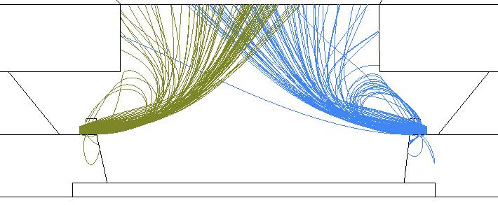
180 162 (c.4.1) Emitter voltage at kv (a) (b) (c) Figure A.25: Emitter Voltage at kv. Pusher Electrode Voltage at (a) kv, (b) kv (c) kv (d) kv. (c.4.2) Emitter voltage at kv (d) (a) (b) (c) Figure A.26: Emitter Voltage at kv. Pusher Electrode Voltage at (a) kv, (b) kv (c) kv (d) kv. (d)
 Emitter voltage at -22.")


 -22.34 kv (d) -22.")
 Emitter voltage at -22.")

181 163 (c.4.3) Emitter voltage at kv (a) (b) (c) Figure A.27: Emitter Voltage at kv. Pusher Electrode Voltage at (a) kv, (b) kv (c) kv (d) kv. (c.4.4) Emitter voltage at kv (d) (a) (b) (c) Figure A.28: Emitter Voltage at kv. Pusher Electrode Voltage at (a) kv, (b) kv (c) kv (d) kv. (d)
SIMULATION OF A MAGNETRON USING DISCRETE MODULATED CURRENT SOURCES. Sulmer A. Fernández Gutierrez. A dissertation. submitted in partial fulfillment
 SIMULATION OF A MAGNETRON USING DISCRETE MODULATED CURRENT SOURCES by Sulmer A. Fernández Gutierrez A dissertation submitted in partial fulfillment of the requirements for the degree of Doctor of Philosophy
Magnetron. Physical construction of a magnetron
 anode block interaction space cathode filament leads Magnetron The magnetron is a high-powered vacuum tube that works as self-excited microwave oscillator. Crossed electron and magnetic fields are used
A Faceted Magnetron Concept Using Field Emission Cathodes
 Boise State University ScholarWorks Electrical and Computer Engineering Faculty Publications and Presentations Department of Electrical and Computer Engineering 3-1-2011 A Faceted Magnetron Concept Using
Dhanalakshmi College of Engineering Department of ECE EC6701 RF and Microwave Engineering Unit 4 Part A
 Dhanalakshmi College of Engineering Department of ECE EC6701 RF and Microwave Engineering Unit 4 Part A 1. What is magnetron? [N/D-16] an electron tube for amplifying or generating microwaves, with the
R.K.YADAV. 2. Explain with suitable sketch the operation of two-cavity Klystron amplifier. explain the concept of velocity and current modulations.
 Question Bank DEPARTMENT OF ELECTRONICS AND COMMUNICATION SUBJECT- MICROWAVE ENGINEERING(EEC-603) Unit-III 1. What are the high frequency limitations of conventional tubes? Explain clearly. 2. Explain
High acceleration gradient. Critical applications: Linear colliders e.g. ILC X-ray FELs e.g. DESY XFEL
 High acceleration gradient Critical applications: Linear colliders e.g. ILC X-ray FELs e.g. DESY XFEL Critical points The physical limitation of a SC resonator is given by the requirement that the RF magnetic
Module IV, Lecture 2 DNP experiments and hardware
 Module IV, Lecture 2 DNP experiments and hardware tunnel diodes, Gunn diodes, magnetrons, traveling-wave tubes, klystrons, gyrotrons Dr Ilya Kuprov, University of Southampton, 2013 (for all lecture notes
Highly efficient water heaters using magnetron effects
 Highly efficient water heaters using magnetron effects Technical task of this project is maximum heat output and minimum electric input of power. This research project has several stages of development.
Crossed-Field Amplifier (Amplitron)
") Crossed-Field Amplifier (Amplitron) Figure 1: water-cooled Crossed-Field Amplifier L 4756A in its transport case Figure 2: Subset of the cycloidal electron paths into a Crossed-Field Amplifier Also other
Crossed-Field Amplifier (Amplitron) Figure 1: water-cooled Crossed-Field Amplifier L 4756A in its transport case Figure 2: Subset of the cycloidal electron paths into a Crossed-Field Amplifier Also other
3D ICEPIC simulations of pulsed relativistic magnetron with transparent cathode : a comparative study with 3D MAGIC simulations
 University of New Mexico UNM Digital Repository Electrical and Computer Engineering ETDs Engineering ETDs 8-27-2012 3D ICEPIC simulations of pulsed relativistic magnetron with transparent cathode : a comparative
3. (a) Derive an expression for the Hull cut off condition for cylindrical magnetron oscillator. (b) Write short notes on 8 cavity magnetron [8+8]
![3. (a) Derive an expression for the Hull cut off condition for cylindrical magnetron oscillator. (b) Write short notes on 8 cavity magnetron [8+8]](/thumbs/73/68588725.jpg "3. (a) Derive an expression for the Hull cut off condition for cylindrical magnetron oscillator. (b) Write short notes on 8 cavity magnetron [8+8]") Code No: RR320404 Set No. 1 1. (a) Compare Drift space bunching and Reflector bunching with the help of Applegate diagrams. (b) A reflex Klystron operates at the peak of n=1 or 3 / 4 mode. The dc power
Code No: RR320404 Set No. 1 1. (a) Compare Drift space bunching and Reflector bunching with the help of Applegate diagrams. (b) A reflex Klystron operates at the peak of n=1 or 3 / 4 mode. The dc power
PRINCIPLES OF RADAR. By Members of the Staff of the Radar School Massachusetts Institute of Technology. Third Edition by J.
 PRINCIPLES OF RADAR By Members of the Staff of the Radar School Massachusetts Institute of Technology Third Edition by J. Francis Reintjes ASSISTANT PBOFESSOR OF COMMUNICATIONS MASSACHUSETTS INSTITUTE
DEVELOPMENT OF 100 GHz INTERDIGITAL BACKWARD-WAVE OSCILLATOR
 DEVELOPMENT OF 1 GHz INTERDIGITAL BACKWARD-WAVE OSCILLATOR Masashi Kato, Yukihiro Soga, Tetsuya Mimura, Yasutada Kato, Keiichi Kamada, and Mitsuhiro Yoshida* Graduate School of Natural Science and Technology,
Investigation of Spatial Harmonic Magnetrons for High Power Millimetre and THz Wave Operations
 Investigation of Spatial Harmonic Magnetrons for High Power Millimetre and THz Wave Operations A thesis submitted to the University of London for partial fulfilment of the requirements for the degree of
(i) Determine the admittance parameters of the network of Fig 1 (f) and draw its - equivalent circuit.
 Determine the admittance parameters of the network of Fig 1 (f) and draw its - equivalent circuit.") I.E.S-(Conv.)-1995 ELECTRONICS AND TELECOMMUNICATION ENGINEERING PAPER - I Some useful data: Electron charge: 1.6 10 19 Coulomb Free space permeability: 4 10 7 H/m Free space permittivity: 8.85 pf/m Velocity
I.E.S-(Conv.)-1995 ELECTRONICS AND TELECOMMUNICATION ENGINEERING PAPER - I Some useful data: Electron charge: 1.6 10 19 Coulomb Free space permeability: 4 10 7 H/m Free space permittivity: 8.85 pf/m Velocity
Experimental Verification of the Concept of the Relativistic Magnetron with Simple Mode Converter
 University of New Mexico UNM Digital Repository Electrical and Computer Engineering ETDs Engineering ETDs 5-1-2016 Experimental Verification of the Concept of the Relativistic Magnetron with Simple Mode
2. Achievement of reliable long pulse operation of 1 MW 170 GHz gyrotron
 Demonstration of 1 MW quasi-cw operation of 170 GHz Gyrotron and Progress of EC Technology for ITER A.Kasugai, K.Sakamoto, K.Takahashi, K.Kajiwara, Y.Oda, N.Kobayashi Fusion Research and Development Directorate,
Fast start of oscillations in a short-pulse relativistic magnetron driven by a transparent cathode.
 University of New Mexico UNM Digital Repository Electrical and Computer Engineering ETDs Engineering ETDs 11-7-2011 Fast start of oscillations in a short-pulse relativistic magnetron driven by a transparent
EC 1402 Microwave Engineering
 SHRI ANGALAMMAN COLLEGE OF ENGINEERING & TECHNOLOGY (An ISO 9001:2008 Certified Institution) SIRUGANOOR,TRICHY-621105. DEPARTMENT OF ELECTRONICS AND COMMUNICATION ENGINEERING EC 1402 Microwave Engineering
MAGNETRON DEVELOPMENT. R.R.Moats
 VI. MAGNETRON DEVELOPMENT Prof. S.T.Martin D.L.Eckhardt S.Goldberg V.Mayper R.R.Moats R.Q.Twiss(guest). INTRODUCTION Progress is reported on the following subjects: 1. Results of testing the high-power
Experiment-4 Study of the characteristics of the Klystron tube
 Experiment-4 Study of the characteristics of the Klystron tube OBJECTIVE To study the characteristics of the reflex Klystron tube and to determine the its electronic tuning range EQUIPMENTS Klystron power
Stanford Linear Accelerator Stanford University, Stanford, CA ABSTRACT
 Design of a high power cross field amplifier at X band with an internally coupled waveguide* SLAC-PUB-5416 January 1991 (A) Kenneth Eppley and Kwok Ko Stanford Linear Accelerator Center, Stanford University,
Physics 4BL: Electricity and Magnetism Lab manual. UCLA Department of Physics and Astronomy
 Physics 4BL: Electricity and Magnetism Lab manual UCLA Department of Physics and Astronomy Last revision April 16, 2017 1 Lorentz Force Laboratory 2: Lorentz Force In 1897, only 120 years ago, J.J. Thomson
Navy Electricity and Electronics Training Series
 NONRESIDENT TRAINING COURSE Navy Electricity and Electronics Training Series Module 11 Microwave Principles NAVEDTRA 14183 DISTRIBUTION STATEMENT A: Approved for public release; distribution is unlimited.
INSTITUTE OF AERONAUTICAL ENGINEERING (Autonomous) Dundigal, Hyderabad
 Dundigal, Hyderabad") INSTITUTE OF AERONAUTICAL ENGINEERING (Autonomous) Dundigal, Hyderabad - 500 043 ELECTRONICS AND COMMUNICATION ENGINEERING TUTORIAL BANK Name : MICROWAVE ENGINEERING Code : A70442 Class : IV B. Tech I
INSTITUTE OF AERONAUTICAL ENGINEERING (Autonomous) Dundigal, Hyderabad - 500 043 ELECTRONICS AND COMMUNICATION ENGINEERING TUTORIAL BANK Name : MICROWAVE ENGINEERING Code : A70442 Class : IV B. Tech I
Meshing Challenges in Simulating the Induced Currents in Vacuum Phototriode
 Meshing Challenges in Simulating the Induced Currents in Vacuum Phototriode S. Zahid and P. R. Hobson Electronic and Computer Engineering, Brunel University London, Uxbridge, UB8 3PH UK Introduction Vacuum
St.MARTIN S ENGINEERING COLLEGE Dhulapally, Secunderabad
 St.MARTIN S ENGINEERING COLLEGE Dhulapally, Secunderabad 500014. Department of Electronics and Communication Engineering SUB: MICROWAVE ENGINEERING SECTION: ECE IV A & B NAME OF THE FACULTY: S RAVI KUMAR,T.SUDHEER
Experimental Plan for Testing the UNM Metamaterial Slow Wave Structure for High Power Microwave Generation
 Experimental Plan for Testing the UNM Metamaterial Slow Wave Structure for High Power Microwave Generation Kevin Shipman University of New Mexico Albuquerque, NM MURI Teleseminar August 5, 2016 1 Outline
Normal-conducting high-gradient rf systems
 Normal-conducting high-gradient rf systems Introduction Motivation for high gradient Order of 100 GeV/km Operational and state-of-the-art SwissFEL C-band linac: Just under 30 MV/m CLIC prototypes: Over
Design of ESS-Bilbao RFQ Linear Accelerator
 Design of ESS-Bilbao RFQ Linear Accelerator J.L. Muñoz 1*, D. de Cos 1, I. Madariaga 1 and I. Bustinduy 1 1 ESS-Bilbao *Corresponding author: Ugaldeguren III, Polígono A - 7 B, 48170 Zamudio SPAIN, jlmunoz@essbilbao.org
6 Experiment II: Law of Reflection
 Lab 6: Microwaves 3 Suggested Reading Refer to the relevant chapters, 1 Introduction Refer to Appendix D for photos of the apparatus This lab allows you to test the laws of reflection, refraction and diffraction
arxiv:physics/ v1 [physics.optics] 28 Sep 2005
![arxiv:physics/ v1 [physics.optics] 28 Sep 2005](/thumbs/91/105523130.jpg "arxiv:physics/ v1 [physics.optics] 28 Sep 2005") Near-field enhancement and imaging in double cylindrical polariton-resonant structures: Enlarging perfect lens Pekka Alitalo, Stanislav Maslovski, and Sergei Tretyakov arxiv:physics/0509232v1 [physics.optics]
Near-field enhancement and imaging in double cylindrical polariton-resonant structures: Enlarging perfect lens Pekka Alitalo, Stanislav Maslovski, and Sergei Tretyakov arxiv:physics/0509232v1 [physics.optics]
Examination of Microphonic Effects in SRF Cavities
 Examination of Microphonic Effects in SRF Cavities Christina Leidel Department of Physics, Ohio Northern University, Ada, OH, 45810 (Dated: August 13, 2004) Superconducting RF cavities in Cornell s proposed
Chapter 21. Alternating Current Circuits and Electromagnetic Waves
 Chapter 21 Alternating Current Circuits and Electromagnetic Waves AC Circuit An AC circuit consists of a combination of circuit elements and an AC generator or source The output of an AC generator is sinusoidal
High Power, Magnet-free, Waveguide Based Circulator Using Angular-Momentum Biasing of a Resonant Ring
 SLAC-R-1080 High Power, Magnet-free, Waveguide Based Circulator Using Angular-Momentum Biasing of a Resonant Ring Jeffrey Neilson and Emilio Nanni August 18, 2017 Prepared for Calabazas Creek Research,
Correlation Between Measured and Simulated Parameters of a Proposed Transfer Standard
 Correlation Between Measured and Simulated Parameters of a Proposed Transfer Standard Jim Nadolny AMP Incorporated ABSTRACT Total radiated power of a device can be measured using a mode stirred chamber
The Stub Loaded Helix: A Reduced Size Helical Antenna
 The Stub Loaded Helix: A Reduced Size Helical Antenna R. Michael Barts Dissertation submitted to the Faculty of the Virginia Polytechnic Institute and State University in partial fulfillment of the requirements
QPR No SPONTANEOUS RADIOFREQUENCY EMISSION FROM HOT-ELECTRON PLASMAS XIII. Academic and Research Staff. Prof. A. Bers.
 XIII. SPONTANEOUS RADIOFREQUENCY EMISSION FROM HOT-ELECTRON PLASMAS Academic and Research Staff Prof. A. Bers Graduate Students C. E. Speck A. EXPERIMENTAL STUDY OF ENHANCED CYCLOTRON RADIATION FROM AN
Analysis and Design of Autonomous Microwave Circuits
 Analysis and Design of Autonomous Microwave Circuits ALMUDENA SUAREZ IEEE PRESS WILEY A JOHN WILEY & SONS, INC., PUBLICATION Contents Preface xiii 1 Oscillator Dynamics 1 1.1 Introduction 1 1.2 Operational
Tutorial: designing a converging-beam electron gun and focusing solenoid with Trak and PerMag
 Tutorial: designing a converging-beam electron gun and focusing solenoid with Trak and PerMag Stanley Humphries, Copyright 2012 Field Precision PO Box 13595, Albuquerque, NM 87192 U.S.A. Telephone: +1-505-220-3975
Improved Performance of Magnetrons using the Transparent Cathode 1
 High power microwaves Improved Performance of Magnetrons using the Transparent Cathode 1 H. Bosman, S. Prasad, M. Fuks, and E. Schamiloglu Department of Electrical & Computer Engineering MSC01 1100, 1
QUESTION BANK SUB. NAME: RF & MICROWAVE ENGINEERING SUB. CODE: EC 2403 BRANCH/YEAR/: ECE/IV UNIT 1 TWO PORT RF NETWORKS- CIRCUIT REPRESENTATION
 QUESTION BANK SUB. NAME: RF & MICROWAVE ENGINEERING SUB. CODE: EC 2403 SEM: VII BRANCH/YEAR/: ECE/IV UNIT 1 TWO PORT RF NETWORKS- CIRCUIT REPRESENTATION 1. What is RF? 2. What is an RF tuner? 3. Define
2.2 MW Operation of the European Coaxial-Cavity Pre-Prototype Gyrotron for ITER
 2.2 MW Operation of the European Coaxial-Cavity Pre-Prototype Gyrotron for ITER G. Gantenbein 1, T. Rzesnicki 1, B. Piosczyk 1, S. Kern 1, S. Illy 1, J. Jin 1, A. Samartsev 1, A. Schlaich 1,2 and M. Thumm
OPTIMIZED MAGNET FOR A 250 MEV PROTON RADIOTHERAPY CYCLOTRON
 OPTIMIZED MAGNET FOR A 250 MEV PROTON RADIOTHERAPY CYCLOTRON J. Kim and H. Blosser 1. Introduction The design of a K250 superconducting cyclotron has been recently improved from the original design of
EC Transmission Lines And Waveguides
 EC6503 - Transmission Lines And Waveguides UNIT I - TRANSMISSION LINE THEORY A line of cascaded T sections & Transmission lines - General Solution, Physical Significance of the Equations 1. Define Characteristic
Projects in microwave theory 2017
 Electrical and information technology Projects in microwave theory 2017 Write a short report on the project that includes a short abstract, an introduction, a theory section, a section on the results and
Waves and Sound Practice Test 43 points total Free- response part: [27 points]
![Waves and Sound Practice Test 43 points total Free- response part: [27 points]](/thumbs/87/96934113.jpg "Waves and Sound Practice Test 43 points total Free- response part: [27 points]") Name Waves and Sound Practice Test 43 points total Free- response part: [27 points] 1. To demonstrate standing waves, one end of a string is attached to a tuning fork with frequency 120 Hz. The other end
Name Waves and Sound Practice Test 43 points total Free- response part: [27 points] 1. To demonstrate standing waves, one end of a string is attached to a tuning fork with frequency 120 Hz. The other end
Long Pulse Operation of a High Power Microwave Source with a Metamaterial Loaded Waveguide
 MURI Grad Student Teleseminar Long Pulse Operation of a High Power Microwave Source with a Metamaterial Loaded Waveguide Xueying Lu MIT 02/03/2016 Outline Review of Stage I experiment Jason Hummelt thesis
Development Status of KSTAR LHCD System
 Development Status of KSTAR LHCD System September 24, 2004 Y. S. Bae,, M. H. Cho, W. Namkung Plasma Sheath Lab. Department of Physics, Pohang University of Science and Technology LHCD system overview Objectives
Projects in microwave theory 2009
 Electrical and information technology Projects in microwave theory 2009 Write a short report on the project that includes a short abstract, an introduction, a theory section, a section on the results and
Review Energy Bands Carrier Density & Mobility Carrier Transport Generation and Recombination
 Review Energy Bands Carrier Density & Mobility Carrier Transport Generation and Recombination Current Transport: Diffusion, Thermionic Emission & Tunneling For Diffusion current, the depletion layer is
FAST RF KICKER DESIGN
 FAST RF KICKER DESIGN David Alesini LNF-INFN, Frascati, Rome, Italy ICFA Mini-Workshop on Deflecting/Crabbing Cavity Applications in Accelerators, Shanghai, April 23-25, 2008 FAST STRIPLINE INJECTION KICKERS
A new picosecond Laser pulse generation method.
 PULSE GATING : A new picosecond Laser pulse generation method. Picosecond lasers can be found in many fields of applications from research to industry. These lasers are very common in bio-photonics, non-linear
Electromagnetics, Microwave Circuit and Antenna Design for Communications Engineering
 Electromagnetics, Microwave Circuit and Antenna Design for Communications Engineering Second Edition Peter Russer ARTECH HOUSE BOSTON LONDON artechhouse.com Contents Preface xvii Chapter 1 Introduction
Signal and Noise Measurement Techniques Using Magnetic Field Probes
 Signal and Noise Measurement Techniques Using Magnetic Field Probes Abstract: Magnetic loops have long been used by EMC personnel to sniff out sources of emissions in circuits and equipment. Additional
Optoelectronic Oscillator Topologies based on Resonant Tunneling Diode Fiber Optic Links
 Optoelectronic Oscillator Topologies based on Resonant Tunneling Diode Fiber Optic Links Bruno Romeira* a, José M. L Figueiredo a, Kris Seunarine b, Charles N. Ironside b, a Department of Physics, CEOT,
MICROWAVE ENGINEERING-II. Unit- I MICROWAVE MEASUREMENTS
 MICROWAVE ENGINEERING-II Unit- I MICROWAVE MEASUREMENTS 1. Explain microwave power measurement. 2. Why we can not use ordinary diode and transistor in microwave detection and microwave amplification? 3.
Fundamentals of Electromagnetics With Engineering Applications by Stuart M. Wentworth Copyright 2005 by John Wiley & Sons. All rights reserved.
 Figure 7-1 (p. 339) Non-TEM mmode waveguide structures include (a) rectangular waveguide, (b) circular waveguide., (c) dielectric slab waveguide, and (d) fiber optic waveguide. Figure 7-2 (p. 340) Cross
CHAPTER 2 MICROSTRIP REFLECTARRAY ANTENNA AND PERFORMANCE EVALUATION
 43 CHAPTER 2 MICROSTRIP REFLECTARRAY ANTENNA AND PERFORMANCE EVALUATION 2.1 INTRODUCTION This work begins with design of reflectarrays with conventional patches as unit cells for operation at Ku Band in
Second-Harmonic Fundamental Mode Slotted Peniotron
 Second-Harmonic Fundamental Mode Slotted Peniotron L.J. Dressman*, D.B. McDermott, and N.C. Luhmann, Jr. University of California, Davis *Also NAVSEA, Crane D.A. Gallagher Northrop Grumman Corp. T.A. Spencer
Lab 4. Crystal Oscillator
 Lab 4. Crystal Oscillator Modeling the Piezo Electric Quartz Crystal Most oscillators employed for RF and microwave applications use a resonator to set the frequency of oscillation. It is desirable to
Circular Patch Antenna with CPW fed and circular slots in ground plane.
 Circular Patch Antenna with CPW fed and circular slots in ground plane. Kangan Saxena, USICT, Guru Gobind Singh Indraprastha University, Delhi-75 ---------------------------------------------------------------------***---------------------------------------------------------------------
Waveguides. Metal Waveguides. Dielectric Waveguides
 Waveguides Waveguides, like transmission lines, are structures used to guide electromagnetic waves from point to point. However, the fundamental characteristics of waveguide and transmission line waves
CONTENTS. Note Concerning the Numbering of Equations, Figures, and References; Notation, xxi. A Bridge from Mathematics to Engineering in Antenna
 CONTENTS Note Concerning the Numbering of Equations, Figures, and References; Notation, xxi Introduction: Theory, 1 A Bridge from Mathematics to Engineering in Antenna Isolated Antennas 1. Free Oscillations,
R. J. Jones Optical Sciences OPTI 511L Fall 2017
 R. J. Jones Optical Sciences OPTI 511L Fall 2017 Semiconductor Lasers (2 weeks) Semiconductor (diode) lasers are by far the most widely used lasers today. Their small size and properties of the light output
Optodevice Data Book ODE I. Rev.9 Mar Opnext Japan, Inc.
 Optodevice Data Book ODE-408-001I Rev.9 Mar. 2003 Opnext Japan, Inc. Section 1 Operating Principles 1.1 Operating Principles of Laser Diodes (LDs) and Infrared Emitting Diodes (IREDs) 1.1.1 Emitting Principles
Lecture 6 Fiber Optical Communication Lecture 6, Slide 1
 Lecture 6 Optical transmitters Photon processes in light matter interaction Lasers Lasing conditions The rate equations CW operation Modulation response Noise Light emitting diodes (LED) Power Modulation
REFLECTION INFLUENCE ON OUTPUT FREQUENCY SPECTRUM AT SUBMILLIMETER FREQUENCY TUNABLE GYROTRONS
 REFLECTION INFLUENCE ON OUTPUT FREQUENCY SPECTRUM AT SUBMILLIMETER FREQUENCY TUNABLE GYROTRONS Aripin 1 and B. Kurniawan 2 1. Department of Physics, Faculty of Mathematics and Natural Sciences, Haluoleo
Power-stabilization of high frequency gyrotrons using a double PID feedback control for applications to many high power THz spectroscopy
 Power-stabilization of high frequency gyrotrons using a double PID feedback control for applications to many high power THz spectroscopy Alexei Kuleshov1,2, Keisuke Ueda3 and Toshitaka Idehara2 Institute
EC ANTENNA AND WAVE PROPAGATION
 EC6602 - ANTENNA AND WAVE PROPAGATION FUNDAMENTALS PART-B QUESTION BANK UNIT 1 1. Define the following parameters w.r.t antenna: i. Radiation resistance. ii. Beam area. iii. Radiation intensity. iv. Directivity.
-31- VII. MAGNETRON DEVELOPMENT. Prof. S. T. Martin V. Mayper D. L. Eckhardt R. R. Moats S. Goldberg R. Q. Twiss
 VII. MAGNETRON DEVELOPMENT Prof. S. T. Martin V. Mayper D. L. Eckhardt R. R. Moats S. Goldberg R. Q. Twiss The activities associated with this project may be divided into two groups; (a) development of
Summary of Research Activities on Microwave Discharge Phenomena involving Chalmers (Sweden), Institute of Applied Physics (Russia) and CNES (France)
, Institute of Applied Physics (Russia) and CNES (France)") Summary of Research Activities on Microwave Discharge Phenomena involving Chalmers (Sweden), Institute of Applied Physics (Russia) and CNES (France) J. Puech (1), D. Anderson (2), M.Lisak (2), E.I. Rakova
Summary of Research Activities on Microwave Discharge Phenomena involving Chalmers (Sweden), Institute of Applied Physics (Russia) and CNES (France) J. Puech (1), D. Anderson (2), M.Lisak (2), E.I. Rakova
GSEB QUESTION PAPER PHYSICS
 GSEB QUESTION PAPER PHYSICS Time : 3 Hours Maximum Marks: 100 Instructions : 1. There are four sections and total 60 questions in this question paper. 2. Symbols used in this question paper have their
Lamb Wave Ultrasonic Stylus
 Lamb Wave Ultrasonic Stylus 0.1 Motivation Stylus as an input tool is used with touchscreen-enabled devices, such as Tablet PCs, to accurately navigate interface elements, send messages, etc. They are,
K1200 Stripper Foil Mechanism RF Shielding
 R.F. Note #121 Sept. 21, 2000 John Vincent Shelly Alfredson John Bonofiglio John Brandon Dan Pedtke Guenter Stork K1200 Stripper Foil Mechanism RF Shielding INTRODUCTION... 2 MEASUREMENT TECHNIQUES AND
Microwave and RF Engineering
 Microwave and RF Engineering Volume 1 An Electronic Design Automation Approach Ali A. Behagi and Stephen D. Turner BT Microwave LLC State College, PA 16803 Copyrighted Material Microwave and RF Engineering
"Natural" Antennas. Mr. Robert Marcus, PE, NCE Dr. Bruce C. Gabrielson, NCE. Security Engineering Services, Inc. PO Box 550 Chesapeake Beach, MD 20732
 Published and presented: AFCEA TEMPEST Training Course, Burke, VA, 1992 Introduction "Natural" Antennas Mr. Robert Marcus, PE, NCE Dr. Bruce C. Gabrielson, NCE Security Engineering Services, Inc. PO Box
Plasma Confinement by Pressure of Rotating Magnetic Field in Toroidal Device
 1 ICC/P5-41 Plasma Confinement by Pressure of Rotating Magnetic Field in Toroidal Device V. Svidzinski 1 1 FAR-TECH, Inc., San Diego, USA Corresponding Author: svidzinski@far-tech.com Abstract: Plasma
Experiment 12: Microwaves
 MASSACHUSETTS INSTITUTE OF TECHNOLOGY Department of Physics 8.02 Spring 2005 OBJECTIVES Experiment 12: Microwaves To observe the polarization and angular dependence of radiation from a microwave generator
Exercise 1-3. Radar Antennas EXERCISE OBJECTIVE DISCUSSION OUTLINE DISCUSSION OF FUNDAMENTALS. Antenna types
 Exercise 1-3 Radar Antennas EXERCISE OBJECTIVE When you have completed this exercise, you will be familiar with the role of the antenna in a radar system. You will also be familiar with the intrinsic characteristics
Microwave and optical systems Introduction p. 1 Characteristics of waves p. 1 The electromagnetic spectrum p. 3 History and uses of microwaves and
 Microwave and optical systems Introduction p. 1 Characteristics of waves p. 1 The electromagnetic spectrum p. 3 History and uses of microwaves and optics p. 4 Communication systems p. 6 Radar systems p.
DEPARTMENT OF ELECTRONICS AND COMMUNICATION ENGINEERING QUESTION BANK SUBJECT NAME & CODE: EC2403 & RF AND MICROWAVE ENGINEERING UNIT I
 FATIMA MICHAEL COLLEGE OF ENGINEERING & TECHNOLOGY Senkottai Village, Madurai Sivagangai Main Road, Madurai -625 020 An ISO 9001:2008 Certified Institution DEPARTMENT OF ELECTRONICS AND COMMUNICATION ENGINEERING
Moses E Emetere (Department Of Physics, Federal University Of Technology Minna P.M.B 65, Minna, Nigeria)
") Online Publication Date: 19 January, 2012 Publisher: Asian Economic and Social Society The Physics Of Remodeling The Transmitting Loop Antenna Using The Schrodinger-Maxwell Equation Uno E Uno (Department
Online Publication Date: 19 January, 2012 Publisher: Asian Economic and Social Society The Physics Of Remodeling The Transmitting Loop Antenna Using The Schrodinger-Maxwell Equation Uno E Uno (Department
Figure Cutaway view of the Phasitron tube, which is used as the modulator and upon which the operation of the GE f-m transmitter is based.
 FM Transmission and Reception Pages 130-135 Rider, John. F., and Seymour D. Uslan John F. Rider Publisher, Inc., 1948. THE GENERAL ELECTRIC TRANSMITTER The original f-m transmitters manufactured by the
Lab 12 Microwave Optics.
 b Lab 12 Microwave Optics. CAUTION: The output power of the microwave transmitter is well below standard safety levels. Nevertheless, do not look directly into the microwave horn at close range when the
CHAPTER 5 FINE-TUNING OF AN ECDL WITH AN INTRACAVITY LIQUID CRYSTAL ELEMENT
 CHAPTER 5 FINE-TUNING OF AN ECDL WITH AN INTRACAVITY LIQUID CRYSTAL ELEMENT In this chapter, the experimental results for fine-tuning of the laser wavelength with an intracavity liquid crystal element
TABLE OF CONTENTS CHAPTER NO. TITLE PAGE NO. LIST OF TABLES LIST OF FIGURES LIST OF SYMBOLS AND ABBREVIATIONS
 vi TABLE OF CONTENTS CHAPTER NO. TITLE PAGE NO. ABSTRACT LIST OF TABLES LIST OF FIGURES LIST OF SYMBOLS AND ABBREVIATIONS iii x xi xvii 1 INTRODUCTION 1 1.1 INTRODUCTION 1 1.2 BACKGROUND 2 1.2.1 Types
SAMPLE QUESTION PAPER CLASS-XII. Physics(Theory)
") SAMPLE QUESTION PAPER CLASS-XII Time allowed: 3 Hrs Physics(Theory) Maximum Marks: 70 GENERAL INSTRUCTIONS: 1. All questions are compulsory. 2. There are 29 questions in total. Questions 1 to 8 are very
SAMPLE QUESTION PAPER CLASS-XII Time allowed: 3 Hrs Physics(Theory) Maximum Marks: 70 GENERAL INSTRUCTIONS: 1. All questions are compulsory. 2. There are 29 questions in total. Questions 1 to 8 are very
ELECTROMAGNETIC SHIELDING HANDBOOK FOR WIRED AND WIRELESS EMC APPLICATIONS
 ELECTROMAGNETIC SHIELDING HANDBOOK FOR WIRED AND WIRELESS EMC APPLICATIONS by Anatoly Tsaliovich Kluwer Academic Publishers Boston / London / Dordrecht Contents Foreword Preface xiii xvii 1. INTRODUCTION
Microwave Devices and Circuit Design
 Microwave Devices and Circuit Design Ganesh Prasad Srivastava Vijay Laxmi Gupta MICROWAVE DEVICES and CIRCUIT DESIGN GANESH PRASAD SRIVASTAVA Professor (Retired) Department of Electronic Science University
Stability Analysis of C-band 500-kW Klystron with Multi-cell. Output cavity
 Stability Analysis of C-band 5-kW Klystron with Multi-cell Output cavity Jihyun Hwang Department of Physics, POSTECH, Pohang 37673 Sung-Ju Park and Won Namkung Pohang Accelerator Laboratory, Pohang 37874
An acousto-electromagnetic sensor for locating land mines
 An acousto-electromagnetic sensor for locating land mines Waymond R. Scott, Jr. a, Chistoph Schroeder a and James S. Martin b a School of Electrical and Computer Engineering b School of Mechanical Engineering
Accurate Electromagnetic Simulation and Design of Cyclotron Cavity Masoumeh Mohamadian, Hossein Afarideh, and Mitra Ghergherehchi
 TNS-00652-2016 1 Accurate Electromagnetic Simulation and Design of Cyclotron Cavity Masoumeh Mohamadian, Hossein Afarideh, and Mitra Ghergherehchi Abstract This study simulated and designed a cyclotron
Professor S. T. MHartin D. L. Eckhardt S. Goldberg V. Mayper R. R. Moats W. Rothman R. Q. T iss (guest) Staff:
 Staff:") L------Ill-- -14LUPU-I~U~LU-LIII~-rW~~ -PI--^YI-Fl~i.- i-1 ~-P I - I VI. MAGUETRON DEVELOPIENT Professor S. T. MHartin D. L. Eckhardt S. Goldberg V. Mayper R. R. Moats W. Rothman R. Q. T iss (guest) Introduction.
L------Ill-- -14LUPU-I~U~LU-LIII~-rW~~ -PI--^YI-Fl~i.- i-1 ~-P I - I VI. MAGUETRON DEVELOPIENT Professor S. T. MHartin D. L. Eckhardt S. Goldberg V. Mayper R. R. Moats W. Rothman R. Q. T iss (guest) Introduction.
Equivalent circuit method of π-mode frequency of rising-sun magnetron
 Equivalent circuit method of π-mode frequency of rising-sun magnetron Song Yue *,, Zhao-chuan Zhang, and Dong-ping Gao Key Laboratory of High Power Microwave Sources and Technologies, Institute of Electronics,
Intermediate Physics PHYS102
 Intermediate Physics PHYS102 Dr Richard H. Cyburt Assistant Professor of Physics My office: 402c in the Science Building My phone: (304) 384-6006 My email: rcyburt@concord.edu My webpage: www.concord.edu/rcyburt
point at zero displacement string 80 scale / cm Fig. 4.1
 1 (a) Fig. 4.1 shows a section of a uniform string under tension at one instant of time. A progressive wave of wavelength 80 cm is moving along the string from left to right. At the instant shown, the
UNIT - V WAVEGUIDES. Part A (2 marks)
") Part A (2 marks) UNIT - V WAVEGUIDES 1. What is the need for guide termination? (Nov / Dec 2011) To avoid reflection loss. The termination should provide a wave impedance equal to that of the transmission
Part A (2 marks) UNIT - V WAVEGUIDES 1. What is the need for guide termination? (Nov / Dec 2011) To avoid reflection loss. The termination should provide a wave impedance equal to that of the transmission
SUPPLEMENTARY INFORMATION
 SUPPLEMENTARY INFORMATION doi:10.1038/nature10864 1. Supplementary Methods The three QW samples on which data are reported in the Letter (15 nm) 19 and supplementary materials (18 and 22 nm) 23 were grown
Communication using Synchronization of Chaos in Semiconductor Lasers with optoelectronic feedback
 Communication using Synchronization of Chaos in Semiconductor Lasers with optoelectronic feedback S. Tang, L. Illing, J. M. Liu, H. D. I. barbanel and M. B. Kennel Department of Electrical Engineering,