LDLN ma ultra low-noise LDO with Power Good and soft-start. Datasheet. Features. Applications. Description
|
|
|
- Elisabeth McKinney
- 5 years ago
- Views:
Transcription
1 Datasheet 300 ma ultra low-noise LDO with Power Good and soft-start Features TSOT23-5L Ultra-low output noise: 7.5 µv RMS Operating input voltage range: 1.6 V to 5.5 V Undervoltage lockout Output current up to 300 ma Very low quiescent current:16 µa at no-load Controlled Iq in dropout condition Very low dropout voltage: 100 mv at 200 ma, 150 mv at 300 ma Very high PSRR: Hz, khz Output voltage accuracy: 2% across line, load and temperature Output voltage versions: from 1 V to 5 V, with 50 mv step Logic-controlled electronic shutdown Power Good Output discharge feature Internal soft-start to limit the in-rush current Overcurrent and thermal protections Temperature range: from -40 C to +125 C Package: TSOT23-5L Maturity status link LDLN030 Device summary Order code LDLN030G33R Package TSOT23-5L Output voltage 3.3 V Applications Smartphones/tablets Image sensors Instrumentation VCO and RF modules HDD and SSD Portable and other battery powered devices Marking Packing KN33 Tape and reel Description The LDLN030 is a 300 ma very low-dropout voltage regulator, able to work with an input voltage ranging from 1.6 V to 5.5 V. The typical dropout voltage at 300 ma load is 150 mv. The very low quiescent current, which is just 16 μa at no load, extends battery-life of applications requiring very long standby time. Thanks to its ultra low-noise value and high PSRR the device provides a very clean output, suitable for ultra-sensitive loads. It is stable with ceramic capacitors. The enable logic control function puts the LDLN030 into shutdown mode allowing a total current consumption lower than 1 μa. The device also includes short-circuit constant current limiting, undervoltage lockout, soft-start, Power Good and thermal protection. Typical applications are noise sensitive loads such as ADC, VCO in mobile phones and tablets, wireless lan devices. The LDLN030 is designed to keep the quiescent DS Rev 1 - February 2018 For further information contact your local STMicroelectronics sales office.
2 current under control and at a low value also during dropout operation, helping to extend even more the operating time of battery-powered devices. DS Rev 1 page 2/21
3 Diagram 1 Diagram Figure 2. Block diagram V IN V OUT Bias generator EN Enable Thermal protection Bandgap reference POWER GOOD GND PG DS Rev 1 page 3/21
4 Pin configuration 2 Pin configuration Figure 3. Pin connection (top view) IN 1 5 OUT GND 2 EN 3 4 PG Table 1. Pin description Symbol TSOT23-5L Description V IN 1 LDO supply voltage V OUT 5 LDO output voltage GND 2 Ground EN 3 Enable input: set V EN = high to turn on the device; V EN = low to turn off the device. Do not left floating. PG 4 Power Good DS Rev 1 page 4/21
5 Typical application diagram 3 Typical application diagram Figure 4. Application diagram V IN V OUT V I V O OFF ON E N L DL N k C IN P G C OUT 1µF G ND 1µF DS Rev 1 page 5/21
6 Maximum ratings 4 Maximum ratings Table 2. Absolute maximum ratings Symbol Parameter Value Unit V IN Input supply voltage -0.3 to 7 V V OUT Output voltage -0.3 to V IN V I OUT Output current Internally limited A EN Enable pin voltage -0.3 to V IN V P D Power dissipation Internally limited W ESD Charge device model ± 1000 V Human body model ± 2000 T J-OP Operating junction temperature - 40 to 125 C T J-MAX Maximum junction temperature 150 C T STG Storage temperature - 55 to 150 C Table 3. Thermal data Symbol Parameter Value Unit R thja Thermal resistance junction-ambient 202 C/W DS Rev 1 page 6/21
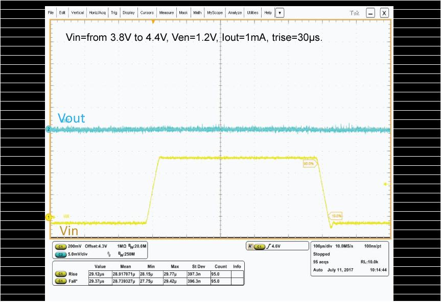
7 Electrical characteristics 5 Electrical characteristics - 40 C < T J < 125 C, typical values refer to T J = 25 C, V IN = V OUT (nom) + 1 V or 1.6 V, whichever is greater; V EN = 1.2 V; C IN = 1 µf; C OUT = 1 µf; I OUT = 1 ma. Table 4. Electrical characteristics Symbol Parameter Test conditions Min. Typ. Max. Unit V IN Operating input voltage range T J = 25 C V V UVLO Undervoltage lockout V IN rising V V OUT Output voltage accuracy (1) V OUT + 1 V < V IN < 5.5 V,1 ma < I OUT < 0.25 A, V OUT 1.8 V V OUT + 1 V < V IN < 5.5 V, 1mA < I OUT < 0.25 A, V OUT < 1.8 V % ΔV OUT / ΔV IN Static line regulation (1) V OUT V < V IN < 5.5 V; µv/v Line transient (2) ΔV IN = +/- 0.6 V, t rise = t fall = 30 μs +/-1 mv ΔV OUT /ΔI OUT Static load regulation 0 ma < I OUT < 0.2 A; µv/ma 1 ma < I OUT < 0.3 A %/ma Load transient (2) I OUT = 1 ma to 200 ma and back t rise = t fall = 1 µs +/-90 mv V DROP Dropout voltage (3) I OUT = 0.1 A; V OUT = 3.3 V 50 mv I OUT = 0.2A; V OUT = 3.3 V I OUT = 0.3 A; V OUT = 3.3 V en Output noise voltage (2) f = 10 Hz to 100 khz; I OUT = 1 ma 10 µv RMS f = 10 Hz to 100 khz; I OUT = 0.2 A f = 10 Hz to 100 khz; I OUT = 0.3 A 7.5 SVR Supply voltage rejection (2) f = 100 Hz; I OUT = 20 ma 80 db f = 1 khz ; I OUT = 20 ma 80 f = 10 khz ; I OUT = 20 ma 75 f = 100 khz ; I OUT = 20 ma 60 f = 100 Hz; I OUT = 150 ma 70 f = 1 khz ; I OUT = 150 ma 68 f = 10 khz ; I OUT = 150 ma 53 I Q Quiescent current I OUT = 0 A, including enable current µa I OUT = 0.2 A I OUT = 0.3 A Shutdown current V EN = 0 V µa I SC Short-circuit current V OUT = 0 V ma R LOW Output discharge resistance V EN = 0 V, de-assert V EN from V EN_HI to V EN_LO Ω V EN V IL, enable input logic low V OUT + 1 V (1) < V IN < 5.5 V 0.4 V V IH, enable input logic high 1.2 DS Rev 1 page 7/21
8 Electrical characteristics Symbol Parameter Test conditions Min. Typ. Max. Unit I EN Enable pin input current V IN = V EN = 5.5 V (pull-down) 5 µa t ON1 Rise time (SS) (2) I OUT = 0 ma to 200 ma for V OUT = 10% V OUT(nom) to 95% V OUT(nom) 200 µs t ON2 Turn-on time (2) I OUT = 0 ma to 200 ma, from V EN assertion to 95% of V OUT(nom) µs T SHDN Thermal shutdown (2) I OUT > 1 ma C Hysteresis (2) 20 V PG- Power Good threshold V OUT decreasing %V OUT voltage V PG+ V OUT increasing PG HYS Power Good hysteresis Measured at V OUT 2 %V OUT PG L Power Good output low De-assert V EN from V EN_HI to V EN_LO V PG IL Power Good pin leakage Measured at V OUT µa current (2) PG RT Power Good reaction time (2) 2 10 µs PG RD Power Good delay (2) 2 10 µs 1. V IN = V OUT + 1 V or 1.6 V, whichever is greater. Not applicable for 5 V output voltage versions. 2. Performance guaranteed by design and/or characterization, and not production tested. 3. Dropout voltage is the input-to-output voltage difference at which the output voltage is 100 mv below its nominal value. Note: Performance guaranteed over the indicated operating temperature range by design and/or characterization, and/or production tested at T J = T A = 25 C. Low duty cycle pulse techniques are used during testing to maintain the junction temperature as close to ambient as possible. Table 5. Recommended input and output capacitors Symbol Parameter Test conditions Min. Typ. Max. Unit C IN Input capacitance Stability µf C OUT Output capacitance ESR Output/input capacitance mω DS Rev 1 page 8/21
9 Typical characteristics 6 Typical characteristics The following plots are referred to LDLN030 in the typical application circuit and, unless otherwise noted, at T A = 25 C. Figure 5. Output voltage vs. temperature (V IN = 4.3 V, I OUT = 1 ma) Figure 6. Output voltage vs. temperature (V IN = 4.3 V, I OUT = 300 ma) Vout (V) Vout (V) Figure 7. Load regulation vs. temperature (V IN = 4.3 V, I OUT from 1 ma to 300 ma) Figure 8. Line regulation vs. temperature (V IN from 4.3 V to 5.5 V, I OUT = 1 ma) (%/ma) (mv/v) Figure 9. Quiescent current vs. temperature, (I OUT = 0 ma) Figure 10. Quiescent current vs. temperature, (I OUT = 200 ma) 30 Iq [µa] Iq [µa] DS Rev 1 page 9/21
![Typical characteristics Figure 11. UVLO vs. temperature Figure 12. PG threshold vs. temperature Vin [V] 1.6 1.5 1.4 1.3 1.2 On 1.](/docs-images/80/81461827/images/10-0.jpg "1 Off 1-40 -15 10 35 60 85 110 135 Vout [V] 3.3 3.2 3.1 3 2.9 On 2.8 Off 2.7-40 -15 10 35 60 85 110 135 Figure 13. Power Good transient Figure 14.")

10 Typical characteristics Figure 11. UVLO vs. temperature Figure 12. PG threshold vs. temperature Vin [V] On 1.1 Off Vout [V] On 2.8 Off Figure 13. Power Good transient Figure 14. Power Good transient Figure 15. Dropout voltage vs. temperature I OUT = 100 ma Figure 16. Dropout voltage vs. temperature I OUT = 200 ma Vdrop (mv) Vdrop (mv) Temp [ C] DS Rev 1 page 10/21
![Typical characteristics Figure 17. Output voltage vs. input voltage Figure 18. Short-circuit current vs. temperature 3.5 3 2.5 0.6 0.5 Vout = 0 Vout [V] 2 1.5 1 0.5 0 0 1 2 3 4 5 Vin [V] Isc [A] 0.](/docs-images/80/81461827/images/11-0.jpg "4 0.3 0.2 0.1 0-60 -40-20 0 20 40 60 80 100 120 140 Figure 19. R discharge vs. temperature Figure 20. Stability region vs. C OUT and ESR 500 450 400 Output discharge resistance Ven = 0, Vin = 4.")
![3 V Rlow [Ohm] 350 300 250 200 150 100 50 0-60 -40-20 0 20 40 60 80 100 120 140 Figure 21. PSRR vs. frequency Figure 22. Noise density vs. frequency 90 80 10.](/docs-images/80/81461827/images/11-1.jpg "000 Magnitude (db) 70 60 50 40 30 20 10 Test condition: Vin=Vout+1V Vripple=200mV Cout=1uF MLCC 20mA 150mA 300mA 0 0.01 0.10 1.00 10.00 100.00 1,000.")
11 Typical characteristics Figure 17. Output voltage vs. input voltage Figure 18. Short-circuit current vs. temperature Vout = 0 Vout [V] Vin [V] Isc [A] Figure 19. R discharge vs. temperature Figure 20. Stability region vs. C OUT and ESR Output discharge resistance Ven = 0, Vin = 4.3 V Rlow [Ohm] Figure 21. PSRR vs. frequency Figure 22. Noise density vs. frequency Magnitude (db) Test condition: Vin=Vout+1V Vripple=200mV Cout=1uF MLCC 20mA 150mA 300mA , Frequency (khz) Output Noise Density: [mv/sqrt(hz)] Test condition: V IN = 4.3V V EN = 1.2V V OUT = 3.3V (Fixed) T a = 25 o C Cin=Cout=1μF(MLCC) Frequency: f [khz] 1mA 200mA 300mA DS Rev 1 page 11/21


12 Typical characteristics Figure 23. Line transient Figure 24. Load transient Figure 25. Load transient Figure 26. Inrush current Figure 27. Enable transient Figure 28. Enable transient DS Rev 1 page 12/21
13 Package information 7 Package information In order to meet environmental requirements, ST offers these devices in different grades of ECOPACK packages, depending on their level of environmental compliance. ECOPACK specifications, grade definitions and product status are available at: ECOPACK is an ST trademark. DS Rev 1 page 13/21
14 TSOT23-5L package information 7.1 TSOT23-5L package information Figure 29. TSOT23-5L package outline POA_ Table 6. TSOT23-5L mechanical data Dim. mm Min. Typ. Max. A 1.00 A A b b e e BSC 1.90 BSC c c D E E BSC 2.80 BSC 1.60 BSC L L1 L REF 0.25 BSC DS Rev 1 page 14/21
15 TSOT23-5L package information Dim. mm Min. Typ. Max. R 0.10 R ɵ ɵ N 5 Figure 30. TSOT23-5L tape and reel drawing W Note: Drawing not in scale Table 7. TSOT23-5L tape and reel Dim. mm Min. Typ. Max. A 180 C D 20.2 N 60 T 14.4 Ao Bo Ko DS Rev 1 page 15/21
16 TSOT23-5L package information Dim. mm Min. Typ. Max. Po P W 8.0 Figure 31. TSOT23-5L footprint data (dimensions are in mm) DS Rev 1 page 16/21
17 Revision history Date Revision Changes 08-Feb Initial release. Table 8. Document revision history DS Rev 1 page 17/21
18 Contents Contents 1 Diagram Pin configuration Typical application diagram Maximum ratings Electrical characteristics Typical characteristics Package information TSOT23-5L package information...14 Revision history...17 DS Rev 1 page 18/21
19 List of tables List of tables Table 1. Pin description....4 Table 2. Absolute maximum ratings...6 Table 3. Thermal data....6 Table 4. Electrical characteristics...7 Table 5. Recommended input and output capacitors...8 Table 6. TSOT23-5L mechanical data Table 7. TSOT23-5L tape and reel Table 8. Document revision history DS Rev 1 page 19/21
20 List of figures List of figures Figure 2. Block diagram...3 Figure 3. Pin connection (top view)... 4 Figure 4. Application diagram....5 Figure 5. Output voltage vs. temperature (V IN = 4.3 V, I OUT = 1 ma)...9 Figure 6. Output voltage vs. temperature (V IN = 4.3 V, I OUT = 300 ma)...9 Figure 7. Load regulation vs. temperature (V IN = 4.3 V, I OUT from 1 ma to 300 ma)...9 Figure 8. Line regulation vs. temperature (V IN from 4.3 V to 5.5 V, I OUT = 1 ma)...9 Figure 9. Quiescent current vs. temperature, (I OUT = 0 ma)...9 Figure 10. Quiescent current vs. temperature, (I OUT = 200 ma)...9 Figure 11. UVLO vs. temperature Figure 12. PG threshold vs. temperature Figure 13. Power Good transient Figure 14. Power Good transient Figure 15. Dropout voltage vs. temperature I OUT = 100 ma Figure 16. Dropout voltage vs. temperature I OUT = 200 ma Figure 17. Output voltage vs. input voltage Figure 18. Short-circuit current vs. temperature Figure 19. R discharge vs. temperature Figure 20. Stability region vs. C OUT and ESR Figure 21. PSRR vs. frequency Figure 22. Noise density vs. frequency Figure 23. Line transient Figure 24. Load transient Figure 25. Load transient Figure 26. Inrush current Figure 27. Enable transient Figure 28. Enable transient Figure 29. TSOT23-5L package outline Figure 30. TSOT23-5L tape and reel drawing Figure 31. TSOT23-5L footprint data (dimensions are in mm) DS Rev 1 page 20/21
21 IMPORTANT NOTICE PLEASE READ CAREFULLY STMicroelectronics NV and its subsidiaries ( ST ) reserve the right to make changes, corrections, enhancements, modifications, and improvements to ST products and/or to this document at any time without notice. Purchasers should obtain the latest relevant information on ST products before placing orders. ST products are sold pursuant to ST s terms and conditions of sale in place at the time of order acknowledgement. Purchasers are solely responsible for the choice, selection, and use of ST products and ST assumes no liability for application assistance or the design of Purchasers products. No license, express or implied, to any intellectual property right is granted by ST herein. Resale of ST products with provisions different from the information set forth herein shall void any warranty granted by ST for such product. ST and the ST logo are trademarks of ST. All other product or service names are the property of their respective owners. Information in this document supersedes and replaces information previously supplied in any prior versions of this document STMicroelectronics All rights reserved DS Rev 1 page 21/21
LDLN ma ultra low noise LDO. Applications. Description. Features. Smartphones/tablets Image sensors Instrumentation VCO and RF modules
 250 ma ultra low noise LDO Datasheet - production data Applications Smartphones/tablets Image sensors Instrumentation VCO and RF modules Features Ultra low output noise: 6.5 μvrms Operating input voltage
Description. consumption lower than 1 µa. The device also Input voltage from 2.4 to 5.5 V
 LD59015 150 ma low noise high PSRR linear voltage regulator Description Datasheet - production data The LD59015 provides 150 ma maximum current with an input voltage range from 2.4 V to 5.5 V, and a typical
150 ma low quiescent current and low noise voltage regulator. Description
 LD39015 150 ma low quiescent current and low noise voltage regulator Datasheet - production data Compatible with ceramic capacitors C O = 1 µf Internal current and thermal limit Temperature range: -40
LD A very low dropout fast transient ultra-low noise linear regulator. Datasheet. Features. Applications. Description
 Datasheet 1 A very low dropout fast transient ultra-low noise linear regulator Features Input voltage from 1.8 to 5.5 V Ultra-low dropout voltage (120 mv typ. at 1 A load and V OUT = 3.3 V) Very low quiescent
LD3985. Ultra low drop and low noise BiCMOS voltage regulators. Features. Description
 Ultra low drop and low noise BiCMOS voltage regulators Datasheet - production data Features Input voltage from 2.5 V to 6 V Stable with low ESR ceramic capacitors Ultra low-dropout voltage (60 mv typ.
LDFM. 500 ma very low drop voltage regulator. Applications. Description. Features
 500 ma very low drop voltage regulator Applications Datasheet - production data Features Input voltage from 2.5 to 16 V Very low dropout voltage (300 mv max. at 500 ma load) Low quiescent current (200
Description. Table 1. Device summary. Order codes Output voltage
 High input voltage 85 ma LDO linear regulator Applications Datasheet - production data Mobile phones Industrial battery-powered systems Features 4.3 V to 24 V input voltage 3x3 Low-dropout voltage (500
300 ma very low quiescent current linear regulator IC with automatic green mode
 Datasheet 3 ma very low quiescent current linear regulator IC with automatic green mode Features Input voltage from 1.4 to 5.5 V Ultra low dropout voltage (3 mv typ. at 3 ma load) Automatic green mode
LD39030SJ285R. 300 ma low quiescent current soft-start, low noise voltage regulator. Applications. Description. Features
 LD393SJ 3 ma low quiescent current soft-start, low noise voltage regulator Applications Datasheet - production data Mobile phones Personal digital assistants (PDAs) Cordless phones and similar battery-powered
Description. Table 1. Device summary. Order codes. SOT23-5L Marking SOT323-5L Marking DFN8 (3x3 mm) Marking
 Marking") High input voltage, 85 ma LDO linear regulator Applications Datasheet - production data Mobile phones Personal digital assistant (PDAs) SOT23-5L DFN8 (3x3 mm) Cordless phones and similar battery-powered
High input voltage, 85 ma LDO linear regulator Applications Datasheet - production data Mobile phones Personal digital assistant (PDAs) SOT23-5L DFN8 (3x3 mm) Cordless phones and similar battery-powered
300 ma very low quiescent current linear regulator IC with automatic green mode
 Datasheet 3 ma very low quiescent current linear regulator IC with automatic green mode Features Input voltage from 1.4 to 5.5 V Ultra low dropout voltage (3 mv typ. at 3 ma load) Automatic green mode
LDK ma low quiescent current very low noise LDO (automotive for SOT23-5L package) Applications. Description. Features
 Applications. Description. Features") 3 ma low quiescent current very low noise LDO (automotive for SOT23-5L package) Applications Datasheet - production data DFN6 1.2x1.3 Mobile phones Portable consumer and industrial devices Cordless phones
3 ma low quiescent current very low noise LDO (automotive for SOT23-5L package) Applications Datasheet - production data DFN6 1.2x1.3 Mobile phones Portable consumer and industrial devices Cordless phones
Very low drop and low noise BiCMOS 300 ma voltage regulator. Description. put a part of the board in standby, decreasing the 100 mv step
 Very low drop and low noise BiCMOS 300 ma voltage regulator Datasheet - production data Features Logic-controlled electronic shutdown Internal current and thermal limit Low output voltage noise: 30 µ VRMS
LD39130S. 300 ma very low quiescent current linear regulator IC with the automatic green mode. Applications. Description. Features
 300 ma very low quiescent current linear regulator IC with the automatic green mode Applications Datasheet - production data Features Input voltage from 1.4 to 5.5 V Ultra low dropout voltage (300 mv typ.
Description. Table 1: Device summary
 800 ma ultra low drop, high PSRR voltage regulator Datasheet - production data Features Input voltage from 1 to 5.5 V Ultra low-dropout voltage (90 mv max. @ 800 ma load) Low ground current (35 μa typ.
STLQ ma ultra-low quiescent current LDO. Description. Features. Applications
 200 ma ultra-low quiescent current LDO Datasheet - production data Features Operating input voltage range: 2 V to 5.5 V Output current up to 200 ma Ultra-low quiescent current: 300 na typ. at no load (ADJ
LDK ma low quiescent current very low noise LDO. Applications. Description. Features
 LDK12 2 ma low quiescent current very low noise LDO Applications Datasheet - production data Mobile phones Personal digital assistants (PDAs) Cordless phones and similar battery-powered systems Digital
Description. Table 1. Device summary KF25BD-TR KF25BDT-TR 2.5 V KF33BD-TR KF33BDT-TR 3.3 V KF50BD-TR KF50BDT-TR 5 V KF80BDT-TR
 Very low drop voltage regulators with inhibit Description Datasheet - production data Features SO-8 DPAK Very low dropout voltage (0.4 V) Very low quiescent current (typ. 50 µa in OFF mode, 500 µa in ON
LD ma very low quiescent current linear regulator IC. applications. Description. Features SOT23-5L. DFN4 1x1
 200 ma very low quiescent current linear regulator IC Datasheet - production data DFN4 1x1 SOT23-5L Applications Mobile phones Personal digital assistants (PDAs) Digital still cameras (DSC) Cordless phones
LDK ma high accuracy and high PSRR voltage regulator. Applications. Description. Features. DSC TV BD, DVD PC Industrial
 200 ma high accuracy and high PSRR voltage regulator Datasheet - production data Features SOT23-5L SOT-8 9 Input voltage from 2.5 to 18 V Very low-dropout voltage (100 mv typ. @ 100 ma load) Low quiescent
LD ma very low quiescent current linear regulator IC. applications. Description. Features
 300 ma very low quiescent current linear regulator IC Datasheet - production data Applications Mobile phones Tablets Digital still cameras (DSC) Cordless phones and similar batterypowered systems Portable
LD A low-dropout linear regulator with programmable soft-start. Datasheet. Features. Applications. Description
 Datasheet 1.5 A low-dropout linear regulator with programmable soft-start Features DFN10 3 x 3 wettable flanks Designed for automotive applications Dual supply pins V IN : 0.8 V to 5.5 V V BIAS : 2.7 V
LDL A high PSRR low-dropout linear voltage regulator. Applications. Description. Features
 1.2 A high PSRR low-dropout linear voltage regulator Datasheet - production data Applications Consumer Industrial SMPS Motherboard P.O.L. DC-DC post-regulation Features Input voltage from 2.5 V to 18 V
Description. Table 1. Device summary
 Very low drop and low noise BiCMOS 300 ma voltage regulator Datasheet - production data SOT23-5L Features Input voltage from 2.5 V to 6 V Stable with low ESR ceramic capacitors Very low dropout voltage
LDS3985xx. Ultra low drop-low noise BiCMOS 300 ma voltage regulator for use with very low ESR output capacitor. Features.
 Ultra low drop-low noise BiCMOS 300 ma voltage regulator for use with very low ESR output capacitor Features Input voltage from 2.5 V to 6 V Stable with low ESR ceramic capacitors Ultra low dropout voltage
LD A, low quiescent current, low-noise voltage regulator. Applications. Description. Features
 1 A, low quiescent current, low-noise voltage regulator Datasheet - production data Features DFN6 (3x3 mm) AEC-Q100 qualified Input voltage from 1.5 to 5.5 V Ultra-low dropout voltage (200 mv typ. at 1
LDF. 1 A very low drop voltage regulator. Applications. Description. Features
 1 A very low drop voltage regulator Datasheet - production data Applications Computer and laptop Battery-powered equipments Industrial and medical equipment Consumer and set-top box Features Input voltage
1 Diagram Pin configuration Typical application Maximum ratings Electrical characteristics... 7
 2 ma low quiescent current very low noise LDO Applications Datasheet - production data Mobile phones Personal digital assistants (PDAs) Cordless phones and similar battery-powered systems Digital still
Description. Part numbers Order codes Packages Output voltages
 LDFM LDFM5 5 ma very low drop voltage regulator Datasheet production data Features Input voltage from 2.5 to 16 V Very low dropout voltage (3 mv max. at 5 ma load) Low quiescent current (2 µa typ. @ 5
TSOT23-5L. Description. systems. Regulator ground current increases Input voltage from 2.5 V to 6 V
 Ultra low drop and low noise BiCMOS voltage regulators Flip-chip (1.57 x 1.22) SOT23-5L TSOT23-5L Datasheet - production data Internal current and thermal limit Output low noise voltage 30 µv RMS over
Obsolete Product(s) - Obsolete Product(s)
 - Obsolete Product(s)") Low drop - Low supply voltage Low ESR capacitor compatible Feature summary Input voltage from 1.7 to 3.6V Ultra low dropout voltage (130mV typ. at 300mA load) Very low quiescent current (110µA typ. at
Low drop - Low supply voltage Low ESR capacitor compatible Feature summary Input voltage from 1.7 to 3.6V Ultra low dropout voltage (130mV typ. at 300mA load) Very low quiescent current (110µA typ. at
LDF. 1 A very low drop voltage regulator. Description. Features. Applications
 1 A very low drop voltage regulator Description Datasheet - production data Features Input voltage from 2.6 to 16 V Very low-dropout voltage (500 mv max. at 1 A load) Low quiescent current (200 µa typ.
LD39150xx Ultra low drop BiCMOS voltage regulator Features Description Typical application
 Ultra low drop BiCMOS voltage regulator Features 1.5 A guaranteed output current Ultra low dropout voltage (200 mv typ. @ 1.5 A load, 40 mv typ. @ 300 ma load) Very low quiescent current (1 ma typ. @ 1.5
TS33. Micropower high precision series voltage reference. Datasheet. Features. Applications. Description. QFN8 1.5x1.5
 Datasheet Micropower high precision series voltage reference Features QFN8 1.5x1.5 Fixed 1.25 V,1.8 V, 2.048 V, 2.5 V, 3.0 V, 3.3 V 4.096 V, 5.0 V output voltage Ultra low operating current: 3.9 μa (typ.)
KF25B, KF33B KF50B, KF80B
 KF25B, KF33B KF50B, KF80B Very low drop voltage regulators with inhibit Datasheet production data Features Very low dropout voltage (0.4 V) Very low quiescent current (typ. 50 µa in OFF mode, 500 µa in
LD3985xx. Ultra low drop-low noise BiCMOS voltage regulators low ESR capacitors compatible. Features. Description
 Ultra low drop-low noise BiCMOS voltage regulators low ESR capacitors compatible Features Input voltage from 2.5 V to 6 V Stable with low ESR ceramic capacitors Ultra low dropout voltage (100 mv typ. at
1.2 A low quiescent current LDO with reverse current protection. Description
 1.2 A low quiescent current LDO with reverse current protection Datasheet - production data Applications Consumer Computer Battery-powered systems Low voltage point-of-load USB-powered devices Features
Low noise and low drop voltage regulator with shutdown function. Description
 Low noise and low drop voltage regulator with shutdown function Features SOT23-5L Description Datasheet - production data The LK112S is a low-dropout linear regulator with shutdown function. The internal
ST1S A, 1.5 MHz adjustable, step-down switching regulator. Description. Features
 1.5 A, 1.5 MHz adjustable, step-down switching regulator Description Datasheet - production data Features DFN6D (3 x 3 mm) Step-down current mode PWM (1.5 MHz) DC-DC converter 2% DC output voltage tolerance
Description. Table 1: Device summary LE30CD-TR 3 LE33CD-TR LE33CZ-AP LE33CZ-TR 3.3 LE45CD-TR 4.5 LE50ABD-TR LE33ABZ-AP 5 LE50CD-TR 5 LE80CD-TR 8
 ery low-dropout voltage regulator with inhibit function Datasheet - production data Features ery low-dropout voltage (0.2 typ.) ery low quiescent current (typ. 50 µa in OFF mode, 0.5 ma in ON mode, no
LD A, very low drop voltage regulators. Features. Description. Table 1. Device summary
 3 A, very low drop voltage regulators Datasheet - production data Table 1. Device summary Order codes LD29300P2M33R LD29300P2MTR Output voltages 3.3 V ADJ P²PAK/A Features Very low dropout voltage (typ.
STEF12. Electronic fuse for 12 V line. Description. Features. Applications
 Electronic fuse for 12 V line Description Datasheet - production data Features DFN10 (3x3 mm) Continuous current (typ): 3.6 A N-channel on-resistance (typ): 53 mω Enable/Fault functions Output clamp voltage
Low noise low drop voltage regulator with shutdown function. Part numbers
 Low noise low drop voltage regulator with shutdown function Features Output current up to 150 ma Low dropout voltage (350 mv at I OUT = 50 ma) Very low quiescent current: 0.1 µa in OFF mode and max. 250
LM217, LM V to 37 V adjustable voltage regulators. Datasheet. Features. Description
 Datasheet 1.2 V to 37 V adjustable voltage regulators TO-220 TO-220FP Features Output voltage range: 1.2 to 37 V Output current in excess of 1.5 A 0.1% line and load regulation Floating operation for high
400 ma nano-quiescent synchronous step-down converter with digital voltage selection and Power Good
 Datasheet 400 ma nano-quiescent synchronous step-down converter with digital voltage selection and Power Good Features 500 na input quiescent current at V IN =3.6 V (not switching) 94% typical efficiency
Low noise low drop voltage regulator with shutdown function. Part numbers
 Low noise low drop voltage regulator with shutdown function Features Output current up to 150 ma Low dropout voltage (350 mv at I OUT = 50 ma) Very low quiescent current: 0.1 µa in OFF mode and max. 250
STBC ma standalone linear Li-Ion battery charger with thermal regulation. Datasheet. Features. Applications. Description
 Datasheet 800 ma standalone linear Li-Ion battery charger with thermal regulation Features DFN6 (3 x 3 mm) Programmable charge current up to 800 ma No external MOSFET, sense resistors or blocking diode
L4931. Very low drop voltage regulators with inhibit. Description. Features
 Very low drop voltage regulators with inhibit Datasheet - production data Features Very low dropout voltage (0.4 V) Very low quiescent current Typ. 50 µa in OFF mode, 600 µa in ON mode Output current up
LD A, very low drop voltage regulators. Description. Features
 1.5 A, very low drop voltage regulators Datasheet - production data Description The is a high current, high accuracy, low-dropout voltage regulator series. These regulators feature 400 mv dropout voltage
L4949ED-E L4949EP-E. Automotive multifunction very low drop voltage regulator. Description. Features
 L4949ED-E L4949EP-E Automotive multifunction very low drop voltage regulator Description Datasheet - production data SO-8 SO-20W (12+4+4) The L4949ED-E and L4949EP-E are monolithic integrated 5V voltage
STLQ ma, 3 μa supply current low drop linear regulator. Features. Applications. Description
 50 ma, 3 μa supply current low drop linear regulator Datasheet - production data Features SOT323-5L 2.3 V to 12 V input voltage range 50 ma maximum output current 3 µa quiescent current Available in 1.8
L4949ED-E L4949EP-E. Automotive multifunction very low drop voltage regulator. Description. Features
 L4949ED-E L4949EP-E Automotive multifunction very low drop voltage regulator Description Datasheet - production data SO-8 SO-20W (12+4+4) The L4949ED-E and L4949EP-E are monolithic integrated 5V voltage
LM2931. Very low drop voltage regulators with inhibit function. Description. Features
 Very low drop voltage regulators with inhibit function Description Datasheet - production data DPAK Features SO-8 TO-92 Very low dropout voltage (90 mv typ. at 10 ma load) Low quiescent current (typ. 2.5
TS4061. Precision micropower shunt voltage reference. Description. Features. Applications
 Precision micropower shunt voltage reference Description Datasheet - production data Features Fixed 1.225 V,1.25 V output voltages Ultra low operating current: 10 µa at 25 C High precision @ 25 C: +/-0.1%
L4940xx5 L4940V5 L4940D2T5-TR 5 V L4940xx85 L4940V85 L4940P85 L4940D2T85-TR 8.5 V L4940xx10 L4940D2T10-TR 10 V L4940xx12 L4940D2T12-TR 12 V
 Very low drop 1.5 A regulator Features Precise 5, 8.5, 10, 12 V outputs Low dropout voltage (450 mv typ. at 1 A) Very low quiescent current Thermal shutdown Short circuit protection Reverse polarity protection
LD1085CXX. 3 A low-drop, adjustable positive voltage regulator. Features. Description
 3 A low-drop, adjustable positive voltage regulator Features Typical dropout 1.3 V (at 3 A) Three terminal adjustable output voltage Guaranteed output current up to 3 A Output tolerance ± 2 % at 25 C and
id id mA, Low Dropout, Low Noise Ultra-Fast With Soft Start CMOS LDO Regulator Features General Description Applications
 500mA, Low Dropout, Low Noise Ultra-Fast With Soft Start CMOS LDO Regulator General Description The is a 500mA, low dropout and low noise linear regulator with high ripple rejection ratio. It has fixed
id9309 Ultra-Low Noise Ultra-Fast 300mA LDO Regulator Features
 Ultra-Low Noise Ultra-Fast 300mA LDO Regulator General Description The id9309 is a 300mA, low dropout and low noise linear regulator with high ripple rejection ratio and fast turn-on time. It has fixed
LD1117Axx. Low drop fixed and adjustable positive voltage regulators. Features. Description
 Low drop fixed and adjustable positive voltage regulators Features Low dropout voltage (1.15 V typ. @ I OUT = 1 A, 25 C) Very low quiescent current (5 ma typ. @ 25 C) Output current up to 1 A Fixed output
STOD1812. Power supply for PMOLED display panel. Features. Description. Applications
 STOD1812 Power supply for PMOLED display panel Features Synchronous step-up converter Input voltage range from 2.5 V to 5.5 V Maximum output current 120 ma Efficiency: 75 % at I O = 10 ma - 30 ma; 85 %
ST619LBDR. DC-DC converter regulated 5 V charge pump. Features. Description
 DC-DC converter regulated 5 V charge pump Features Regulated 5 V ±4 % charge pump Output current guaranteed over temperature: 20 ma (V I 2 V), 30 ma (V I 3 V) No inductors; very low EMI noise Uses small,
LExxAB LExxC. Very low dropout voltage regulators with inhibit function. Features. Description
 LExxAB LExxC ery low dropout voltage regulators with inhibit function Datasheet production data Features ery low dropout voltage (0.2 typ.) ery low quiescent current (typ. 50 µa in OFF mode, 0.5 ma in
LD ma very low quiescent current linear regulator IC. applications. Description. Features
 LD39020 200 ma very low quiescent current linear regulator IC Datasheet - production data Applications Mobile phones Personal digital assistants (PDAs) Digital still cameras (DSC) Cordless phones and similar
TO-220 D²PAK TO-220FP
 Negative voltage regulators Datasheet production data Features Output current up to 1.5 A Output voltages of - 5; - 8; - 12; - 15 V Thermal overload protection Short circuit protection Output transition
L79xxC. Negative voltage regulators. Features. Description
 Negative voltage regulators Features Output current up to 1.5 A Output voltages of -5; -8; -12; -15; -20 V Thermal overload protection Short circuit protection Output transition SOA protection Description
Order codes. TO-220 D²PAK (tape and reel) TO-220FP TO-3 LM117K LM217T LM217D2T-TR LM217K LM317T LM317D2T-TR LM317P LM317K
 TO-220FP TO-3 LM117K LM217T LM217D2T-TR LM217K LM317T LM317D2T-TR LM317P LM317K") LM117 LM217, LM317 1.2 V to 37 V adjustable voltage regulators Features Output voltage range: 1.2 to 37 V Output current in excess of 1.5 A 0.1 % line and load regulation Floating operation for high voltages
LM117 LM217, LM317 1.2 V to 37 V adjustable voltage regulators Features Output voltage range: 1.2 to 37 V Output current in excess of 1.5 A 0.1 % line and load regulation Floating operation for high voltages
TSV611, TSV611A, TSV612, TSV612A
 TSV611, TSV611A, TSV612, TSV612A Rail-to-rail input/output 10 µa, 120 khz CMOS operational amplifiers Applications Datasheet - production data Out1 1 In1-2 In1+ 3 TSV611ILT - TSV611ICT In+ 1 5 V CC+ +
STEF033. Electronic fuse for 3.3 V line. Description. Features. Applications
 Electronic fuse for 3.3 V line Description Datasheet - production data DFN10 (3 x 3 mm) Flip Chip 9 Features Continuous current typ.: 3.6 A (DFN), 2.5 A (Flip Chip) N-channel on resistance (typ): 40 mω
ST8R00. Micropower 1 A synchronous step-up DC-DC converter. Features. Description
 ST8R Micropower 1 A synchronous step-up DC-DC converter Features Output voltage adjustable from 6 V to 12 V Output voltage accuracy: ± 2% Output current up to 1 A Low ripple voltage: 5 mv (typ.) Synchronous
LD1085xx. 3 A low drop positive voltage regulator adjustable and fixed. Features. Description
 3 A low drop positive voltage regulator adjustable and fixed Features Typical dropout 1.3 V (at 3 A) Three terminal adjustable or fixed output voltage 1.5 V, 1.8 V, 2.5 V, 3.3 V, 5 V, 12 V. Automotive
LK115XX30 LK115XX33 - LK115XX50
 LK115XX30 LK115XX33 - LK115XX50 ery low drop with inhibit voltage regulators Features ery low dropout voltage (0.2 typ.) ery low quiescent current (Typ. 0.01 µa in off mode, 280 µa in on mode) Output current
TS V adjustable shunt voltage reference. Description. Features. Applications
 1.24 V adjustable shunt voltage reference Datasheet - production data Battery chargers Switch mode power supply Battery operated equipment SOT23-3L (Plastic micropackage) Description The is an adjustable
P-channel -30 V, 12 mω typ., -9 A STripFET H6 Power MOSFET in a PowerFLAT 3.3x3.3 package. Order code V DS R DS(on) max I D
 max I D") Datasheet P-channel -30 V, 12 mω typ., -9 A STripFET H6 Power MOSFET in a PowerFLAT 3.3x3.3 package Features Order code V DS R DS(on) max I D STL9P3LLH6-30 V 15 mω -9 A Very low on-resistance Very low
Datasheet P-channel -30 V, 12 mω typ., -9 A STripFET H6 Power MOSFET in a PowerFLAT 3.3x3.3 package Features Order code V DS R DS(on) max I D STL9P3LLH6-30 V 15 mω -9 A Very low on-resistance Very low
 Distributed by: www.jameco.com 1-800-831-4242 The content and copyrights of the attached material are the property of its owner. 1.5A Low drop positive voltage regulator adjustable and fixed Feature summary
LD3985 SERIES ULTRA LOW DROP-LOW NOISE BICMOS VOLTAGE REGULATORS LOW ESR CAPACITORS COMPATIBLE
 LD3985 SERIES ULTRA LOW DROP-LOW NOISE BICMOS VOLTAGE REGULATORS LOW ESR CAPACITORS COMPATIBLE INPUT VOLTAGE FROM 2.5V TO 6V STABLE WITH LOW ESR CERAMIC CAPACITORS ULTRA LOW DROPOUT VOLTAGE (100mV TYP.
LM2904AH. Low-power, dual operational amplifier. Related products. Description. Features. See LM2904WH for enhanced ESD performances
 LM2904AH Low-power, dual operational amplifier Datasheet - production data Related products See LM2904WH for enhanced ESD performances Features Frequency compensation implemented internally Large DC voltage
Obsolete Product(s) - Obsolete Product(s) Obsolete Product(s) - Obsolete Product(s)
 - Obsolete Product(s) Obsolete Product(s) - Obsolete Product(s)") 5 A low dropout fast response positive voltage regulator adjustable Features Typical dropout 1.2 V Fast transient response Three terminal adjustable Guaranteed output current up to 5 A Output tolerance
5 A low dropout fast response positive voltage regulator adjustable Features Typical dropout 1.2 V Fast transient response Three terminal adjustable Guaranteed output current up to 5 A Output tolerance
STPW12. Programmable electronic power breaker for 12 V bus. Datasheet. Features. Applications. Description
 Datasheet Programmable electronic power breaker for 12 V bus Features Power SO8 Real-time input power sensing Input voltage range: from 10.5 V to 18 V Continuous current typ.: 1.5 A P-channel on resistance
Low Noise 300mA LDO Regulator General Description. Features
 Low Noise 300mA LDO Regulator General Description The id9301 is a 300mA with fixed output voltage options ranging from 1.5V, low dropout and low noise linear regulator with high ripple rejection ratio
YB1210R 300mA, Ultra-Low-Noise, High PSRR LDO Regulator
 Description The YB1210R is a series of ultra-low-noise, low dropout (LDO) linear regulators with 2.0% output voltage accuracy. The YB1210R regulators achieve a low 320mV dropout at 300mA load current of
STP4CMP. Low voltage 4-channel constant current LED driver with charge pump. Description. Features. Applications
 Low voltage 4-channel constant current LED driver with charge pump Datasheet - production data Features Operating voltage range: V CC.7 V to 5.5 V Full RGB function support 4-channel LED driver with individual
TSX339. Micropower quad CMOS voltage comparators. Related products. Applications. Description. Features
 Micropower quad CMOS voltage comparators Datasheet - production data Related products Pin-to-pin and functionally compatible with the quad CMOS TS339 comparators See TSX3704 for push-pull output Applications
STG3693. Low voltage high bandwidth quad SPDT switch. Features. Description
 Low voltage high bandwidth quad SPDT switch Datasheet - production data Features Ultra low power dissipation: I CC = 0.3 µa at T A = 125 C Low on-resistance: R DS(on) = 4 Ω (T A = 25 C) at V CC = 3.0 V
TSC1021. High-side current sense amplifier. Related products. Applications. Features. Description
 High-side current sense amplifier Datasheet - production data Related products See TSC103 for higher common-mode operating range (2.9 V to 70 V) Features Wide common-mode operating range independent of
STCS05A. 0.5 A max constant current LED driver. Features. Applications. Description
 0.5 A max constant current LED driver Features Up to 40 V input voltage Less than 0.5 V voltage overhead Up to 0.5 A output current PWM dimming pin Shutdown pin LED disconnection diagnostic Slope control
Obsolete Product(s) - Obsolete Product(s)
 - Obsolete Product(s)") General features Supply voltage range: 2.6V to 5.5V 17V Maximum output voltage STCF01 Step-up converter for cell phone camera flash LEDs Two current levels up to 300mA set with external resistors Dedicated
General features Supply voltage range: 2.6V to 5.5V 17V Maximum output voltage STCF01 Step-up converter for cell phone camera flash LEDs Two current levels up to 300mA set with external resistors Dedicated
L4949E. Multifunction very low drop voltage regulator. Features. Description
 Multifunction very low drop voltage regulator Features Operating DC supply voltage range 5 V - 28 V Transient supply voltage up to 40V Extremely low quiescent current in standby mode High precision standby
LM323. Three-terminal 3 A adjustable voltage regulators. Description. Features
 Three-terminal 3 A adjustable voltage regulators Description Datasheet - production data Features TO-220 Output current: 3 A Internal current and thermal limiting Typical output impedance: 0.01 Ω Minimum
LD A low drop positive voltage regulator: adjustable and fixed. Features. Description
 3 A low drop positive voltage regulator: adjustable and fixed Datasheet - production data TO-220 TO-220FP Unlike PNP regulators, where a part of the output current is wasted as quiescent current, the LD1085
TS2431. Adjustable shunt voltage reference. Applications. Description. Features
 Adjustable shunt voltage reference Datasheet - production data Industrial temperature range: - 40 to + 105 C Performance compatible with industrystandard TL431 Applications Computers Instrumentation Battery
LM723CN. High precision voltage regulator. Features. Description
 High precision voltage regulator Features Input voltage up to 40 V Output voltage adjustable from 2 to 37 V Positive or negative supply operation Series, shunt, switching or floating operation Output current
RT2904WH. RobuST low-power dual operational amplifier. Applications. Features. Description
 RobuST low-power dual operational amplifier Datasheet - production data Features D SO8 (plastic micropackage) Pin connections (top view) Frequency compensation implemented internally Large DC voltage gain:
N-channel 30 V, 2.5 mω typ., 120 A STripFET H6 Power MOSFET in a TO-220 package. Features. Description
 N-channel 30 V, 2.5 mω typ., 120 A STripFET H6 Power MOSFET in a TO-220 package Datasheet - production data Features Order code V DS R DS(on) max. I D P TOT STP160N3LL 30 V 3.2 mω 120 A 136 W Very low
Description. Table 1. Device summary. Order code Temperature range Package
 ST3232EB ST3232EC ±15 kv ESD protection 3 to 5.5 V low power, up to 250 kbps, RS-232 drivers and receivers Hand-held equipment Peripherals and printers Description Datasheet - production data Features
ST662AB ST662AC. DC-DC converter from 5 V to 12 V, 0.03 A for Flash memory programming supply. Features. Description
 ST662AB ST662AC DC-DC converter from 5 V to 12 V, 0.03 A for Flash memory programming supply Features Output voltage: 12 V ± 5 % Supply voltage range: 4.5 V to 5.5 V Guaranteed output current up to 30
AME. High PSRR, Low Noise, 150mA CMOS Regulator AME8852. n General Description. n Typical Application. n Features. n Functional Block Diagram
 8852 n General Description High PSRR, Low Noise, 15mA n Typical Application The 8852 family of positive, CMOS linear regulators provide low dropout voltage(11mv@15ma), low quiescent current, and low noise
TL1431. Adjustable voltage reference. Features. Description
 Adjustable voltage reference Z TO-92 (Plastic package) L SOT23-5L L SOT23-3L C SOT323-6L Features Datasheet - production data Adjustable output voltage: V REF to 36 V Sink current capability: 1 to 100
LM217M, LM317M. Medium current 1.2 to 37 V adjustable voltage regulator. Description. Features
 Medium current 1.2 to 37 V adjustable voltage regulator Description Datasheet - production data TO-220 DPAK The LM217M and LM317M are monolithic integrated circuits in TO-220 and DPAK packages used as
TS3021H. Automotive rail-to-rail 1.8 V high-speed comparator. Related products. Applications. Description. Features SOT23-5
 Automotive rail-to-rail 1.8 V high-speed comparator Datasheet - production data Related products TS3021 for standard temperature range (-40 C to 125 C) OUT IN+ 1 2 SOT23-5 + - Features AEC-Q100 and Q003
L6932H1.2. High performance 2A ULDO linear regulator. Features. Description. Applications L6932H1.2
 High performance 2A ULDO linear regulator Features 2V to 14V input voltage range 200mΩ r DS(on) max 200µA quiescent current at any load Excellent load and line regulation Adjustable from 1.2V to 5V 1%