XC62H Series GENERAL DESCRIPTION APPLICATIONS FEATURES TYPICAL PERFORMANCE CHARACTERISTICS TYPICAL APPLICATION CIRCUIT
|
|
|
- Daniel Wilson
- 6 years ago
- Views:
Transcription
1 ETR0312_006 Positive Voltage Regulator with (Output ON/OFF) GENERAL DESCRIPTION The XC62H series are highly precise, low power consumption, positive voltage regulators, manufactured using CMOS and laser trimming technologies. The series consists of a high precision voltage reference, an error correction circuit, and an output driver with current limitation. By way of the CE function, with output turned off, the series enters standby. In the stand-by mode, power consumption is greatly reduced. SOT-25 (150mW), SOT-89-5 (500mW) and USP-6B (120mW) packages are available. APPLICATIONS Multi-function power supplies Voltage supplies for cellular phones Digital still cameras / Camcorders Note PC / Tablet PC TYPICAL APPLICATION CIRCUIT FEATURES Maximum Output Current : 165mA (within max Pd, V OUT =3.0V) Output Voltage Range : 2.0V ~ 6.0V (0.1V increments) (1.5V ~ 1.9V semi-custom) Highly Accurate : ±2% (±1% for semi-custom products) Low Power Consumption : 3μA (TYP.) (V OUT =3V,Output enabled) : 0.1μA (TYP.) (Output disabled) Output Voltage Temperature Characteristics : ±100ppm / (TYP.) Line Regulation : 0.2% / V (TYP.) CMOS Low Power Consumption Dropout Voltage : 60mA : 160mA Packages : SOT-25 SOT-89-5 USP-6B Environmentally Friendly :EU RoHS Compliant, Pb Free TYPICAL PERFORMANCE CHARACTERISTICS 1/23
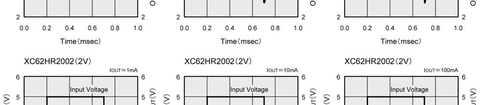
2 PIN CONFIGURATION SOT-25 (TOP VIEW) SOT-89-5 (TOP VIEW) USP-6B (BOTTOM VIEW) *The dissipation pad for the USP-6B package should be solder-plated in recommended mount pattern and metal masking so as to enhance mounting strength and heat release. If the pad needs to be connected to other pins, it should be connected to the VIN (No.1) pin. PIN ASSIGNMENT FUNCTIONS PIN NUMBER SOT-25 SOT-89-5 USP-6B PIN NAME FUNCTIONS 1 4 2, 5 NC No Connection V IN Supply Voltage Input CE ON/OFF Chip Enable V SS Ground V OUT Regulated Output Voltage CE L H OPEN OPERATION OFF ON Undefined state PRODUCT CLASSIFICATION Ordering Information XC62H ( *1 ) DESIGNATOR ITEM SYMBOL DESCRIPTION 1 CE Pin Logic R Positive 23 Output Voltage 20~60 e.g. VOUT 3.0V 2=3, 3=0 VOUT 5.0V 2=5, 3=0 4 Temperature Characteristics ppm (TYP.) 1 + 1% (semi-custom) Output Voltage Accuracy Packages (Order Unit) 2 + 2% MR SOT-25 (3,000/Reel) MR-G SOT-25 (3,000/Reel) PR SOT-89-5 (1,000/Reel) PR-G SOT-89-5 (1,000/Reel) DR USP-6B (3,000/Reel) DR-G USP-6B (3,000/Reel) (*1) The -G suffix denotes Halogen and Antimony free as well as being fully EU RoHS compliant. 2/23
3 XC62H Series BLOCK DIAGRAM ABSOLUTE MAXIMUM RATINGS PARAMETER SYMBOL RATINGS UNITS Input Voltage VIN 12.0 V Output Current IOUT (*1) 500 ma Output Voltage VOUT VSS -0.3 ~ VIN +1.3 V CE Input Voltage VCE VSS -0.3 ~ VIN +1.3 V SOT Power Dissipation SOT-89-5 Pd 500 mw USP-6B 120 Operating Ambient Temperature Topr -30 ~ +80 Storage Temperature Tstg -40 ~ +125 (*1) Please use within the range of I Pd/(V -V ) OUT IN OUT Ta=25 3/23
4 ELECTRICAL CHARACTERISTICS Low Voltage Ta=25 PARAMETER SYMBOL CONDITIONS MIN TYP MAX UNITS CIRCUIT Output Voltage V OUT(E) (*2) V IN =V (*1) OUT(T) +1.0V I OUT =0.5mA E1-1 (*7) E1-2 (*7) V OUT(T) V 1 Maximum Output Current V IN =V OUT(T) +1.0V I OUTmax V OUT(E) V OUT(T) 0.9 E2 (*7) ma 1 Load Regulation ΔV OUT 1mA I OUT 30mA V IN =V OUT(T) +1.0V mv 1 Dropout Voltage (*3) Vdif Output Voltage:1.5 ~ 1.7V I OUT =10mA V CE =V IN Output Voltage:1.8 ~ 1.9V I OUT =20mA V CE =V IN mv 1 Supply Current 1 I SS 1 V IN =V CE =V OUT(T) +1.0V μa 2 Supply Current 2 I SS 2 VIN=V OUT(T) +1.0V,V CE =V SS 0.1 μa 2 Line Regulation ΔV OUT / (ΔV IN V OUT ) I OUT 0.5mA V OUT(T) +1.0V V IN 10V %/V 1 Input Voltage V IN 2 10 V - Output Voltage Temperature Characteristics ΔV OUT / (ΔTopr V OUT ) I OUT =0.5mA -30 Topr 80 ±100 ppm/ 1 CE "High" Voltage V CEH 1.5 V 1 CE "Low" Voltage V CEL 0.25 V 1 CE "High" Current I CEH V CE =V IN 0.1 μa 2 CE "Low" Current I CEL V CE =V SS μa 2 NOTE: *1: V OUT(T) =Specified output voltage. *2: V OUT(E) =Effective output voltage (i.e. the output voltage when "V OUT(T) +1.0V" is provided at the V IN pin while maintaining a certain I OUT value). *3: Vdif= {V IN1 ( * 5) -V OUT1 ( * 4) } *4: V OUT1 = A voltage equal to 98% of the output voltage whenever an amply stabilized I OUT {V OUT(T) +1.0V} is input. *5: V IN1 = The input voltage when V OUT1 appears as input voltage is gradually decreased. *6: Over V IN =2.0V of input voltage is necessary. *7: Refer to the Voltage chart 4/23
5 XC62H Series ELECTRICAL CHARACTERISTICS (Continued) Low Voltage Chart SYMBOL E1-1 E1-2 E2 PARAMETER MAXIMUM OUTPUT SETTING OUTPUT VOLTAGE (V) CURRENT (ma) OUTPUT VOLTAGE(V) V OUT(E) I OUTmax V OUT(T) MIN MAX MIN Note) The symbol is as same as that in the chart of electrical characteristics. 5/23
6 ELECTRICAL CHARACTERISTICS (Continued) Standard Voltage Ta=25 PARAMETER SYMBOL CONDITIONS MIN TYP MAX UNITS CIRCUIT Output Voltage (2%) V IN =V (*1) OUT(T) +1.0V (*2) V OUT(T) V OUT(E) Output Voltage (1%) I OUT =40mA 0.99 E1 (*6) 1.01 V 1 Maximum Output Current V IN =V OUT(T) +1.0V I OUTmax V OUT(E) V OUT(T) 0.9 E2 (*6) ma 1 Load Regulation ΔV OUT 1mA I OUT {C1 (*7) }ma V IN =V OUT(T) +1.0V E3-1 (*6) E3-2 (*6) mv 1 Vdif I OUT ={C2 (*7) }ma E4-1 (*6) E4-2 (*6) mv 1 Dropout Voltage (*3) Vdif I OUT ={C3 (*7) }ma E5-1 (*6) E5-2 (*6) mv 1 Supply Current 1 I SS 1 V IN =V CE =V OUT(T) +1.0V E6-1 (*6) E6-2 (*6) μa 2 Supply Current 2 I SS 2 V IN =V OUT(T) +1.0V,V CE =V SS 0.1 μa 2 Line Regulation ΔV OUT / (ΔV IN V OUT ) I OUT =40mA V OUT(T) +1.0V V IN 10.0V %/V 1 Input Voltage V IN 10 V - Output Voltage Temperature Characteristics ΔV OUT / (ΔTopr V OUT ) I OUT =40mA -30 Topr 80 ±100 ppm/ 1 CE "High" Voltage V CEH 1.5 V 1 CE "Low" Voltage V CEL 0.25 V 1 CE "High" Current I CEH V CE =V IN 0.1 μa 2 CE "Low" Current I CEL V CE =V SS μa 2 NOTE: *1: V OUT(T) =Specified output voltage. *2: V OUT(E) =Effective output voltage (i.e. the output voltage when "V OUT(T) +1.0V" is provided at the V IN pin while maintaining a certain I OUT value). *3: Vdif= {V ( IN1 * 5) -V ( OUT1 * 4) } *4: V OUT1 = A voltage equal to 98% of the output voltage whenever an amply stabilized I OUT {V OUT(T) +1.0V} is input. *5: V IN1 = The input voltage when V OUT1 appears as input voltage is gradually decreased. *6: Refer to the Standard Voltage, Voltage chart *7: Refer to the Voltage chart 6/23
7 XC62H Series ELECTRICAL CHARACTERISTICS (Continued) Standard Voltage, Voltage chart SYMBOL E1-1 E1-2 E2 E3-1 E3-2 E4-1 E4-2 E5-1 E5-2 E6-1 E6-2 SETTING OUTPUT PARAMETER VOLTAGE(V) OUTPUT VOLTAGE (V) (2% products) OUTPUT VOLTAGE (V) (1% products) MAXIMUM OUTPUT CURRENT (ma) LOAD REGULATION (mv) DROPOUT VOLTAGE (mv) SUPPLY CURRENT1 V OUT(E) V OUT(E) I OUTmax ΔV OUT Vdif1 Vdif2 I SS1 V OUT(T) MIN MAX MIN MAX MIN TYP MAX TYP MAX TYP MAX TYP MAX (μa) Note) The symbol is as same as that in the chart of electrical characteristics. 7/23
8 ELECTRICAL CHARACTERISTICS (Continued) Voltage Chart SYMBOL C1 C2 C3 PARAMETER ΔV OUT Vdif1 Vdif2 SETTING CONDITIONS CONDITIONS CONDITIONS OUTPUT VOLTAGE(V) (ma) (ma) (ma) V OUT(T) I OUT I OUT I OUT CONDITIONS CONDITIONS CONDITIONS /23
9 XC62H Series TEST CIRCUITS Circuit 1 Tantalum Tantalum Circuit 2 OPEN 9/23
10 OPERATIONAL EXPLANATION Output voltage control with the XC62H series: The voltage divided by resistors R1 & R2 is compared with the internal reference voltage by the error amplifier. The P-channel MOSFET, which is connected to the VOUT pin, is then driven by the subsequent output signal. The output voltage at the VOUT pin is controlled & stabilized by a system of negative feedback. The current limit circuit operate in relation to the level of output current. < Current Limiter > The XC62H series has output current limiter of fixed current limiter circuit. When the output current reaches the current limit, the fixed current limiter circuit operates and the output voltage drops with keeping the output current. <CE Pin> The IC's internal circuitry can be operated or shutdown via the signal from the CE pin with the XC62H series. In shutdown mode, output at the VOUT pin will be pulled down to the VSS level via R1 & R2. Note that the XC62H series regulator is High Active/No Pull-Down, operations will become unstable with the CE pin open. We suggest that you use this IC with either a CE High level voltage or a CE Low level voltage input at the CE pin. If this IC is used with the correct specifications for the CE pin, the operational logic is fixed and the IC will operate normally. However, supply current may increase as a result of through current in the IC's internal circuitry. <Input and Output Capacitors> The XC62H series needs an output capacitor (C L ) for phase compensation. In order to ensure the stable phase compensation, please place an output capacitor of 1.0μF at the V OUT pin and V SS pin as close as possible. For a stable power input, please connect an input capacitor (C IN ) of 1.0μF between the input pin (V IN ) and the ground pin (V SS ). NOTES ON USE 1. Please use this IC within the stated maximum ratings. For temporary, transitional voltage drop or voltage rising phenomenon, the IC is liable to malfunction should the ratings be exceeded. 2. Where wiring impedance is high, operations may become unstable due to noise and/or phase lag depending on output current. Please strengthen V IN and V SS wiring in particular. 3. Please wire the input capacitor (C IN ) and the output capacitor (C L) as close to the IC as possible. Should rapid input fluctuation or load fluctuation occur, please increase the capacitor value such as CIN or CL to stabilize the operation. 4. Torex places an importance on improving our products and their reliability. We request that users incorporate fail-safe designs and post-aging protection treatment when using Torex products in their systems. 10/23


 Output")
11 XC62H Series TYPICAL PERFORMANCE CHARACTERISTICS (1) Output Voltage vs. Output Current (2) Output Voltage vs. Input Voltage 11/23

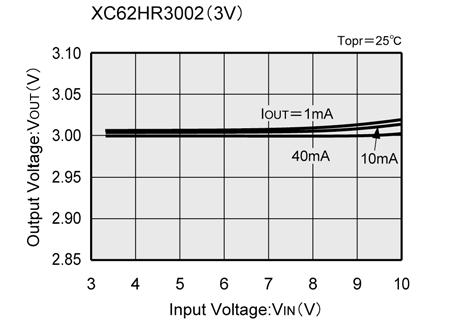
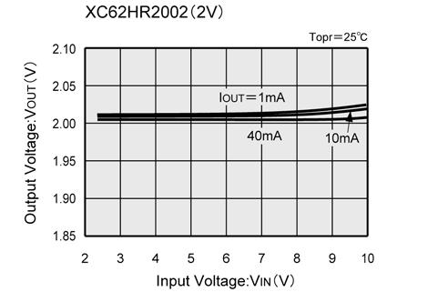
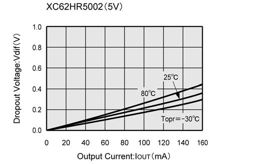
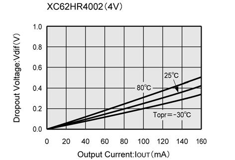
12 TYPICAL PERFORMANCE CHARACTERISTICS (Continued) (2) Output Voltage vs. Input Voltage (Continued) (3) Dropout Voltage vs. Output Current 12/23

 (4) CE Pin")
 Supply")
13 XC62H Series TYPICAL PERFORMANCE CHARACTERISTICS (Continued) (4) CE Pin Threshold Voltage vs. Input Voltage (5) Supply Current vs. Input Voltage 13/23


 (6) Output")
14 TYPICAL PERFORMANCE CHARACTERISTICS (Continued) (5) Supply Current vs. Input Voltage (Continued) (6) Output Voltage vs. Ambient Temperature 14/23


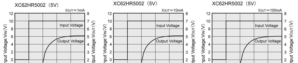
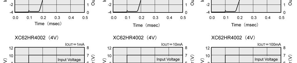
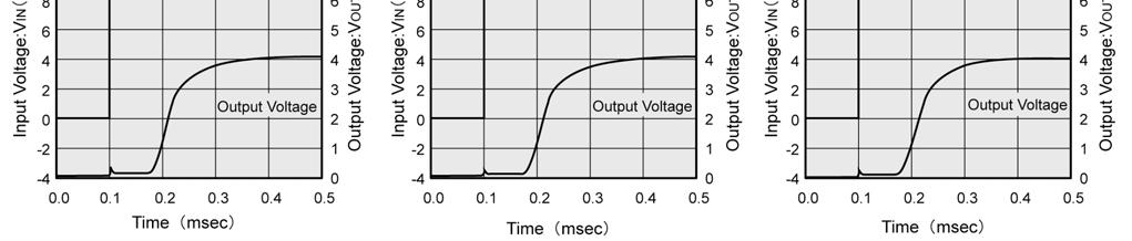
15 XC62H Series TYPICAL PERFORMANCE CHARACTERISTICS (Continued) (7) Supply Current vs. Ambient Temperature (8) Input Transient Response 1 15/23
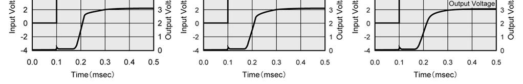
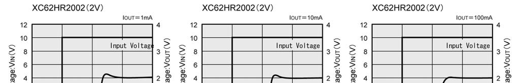

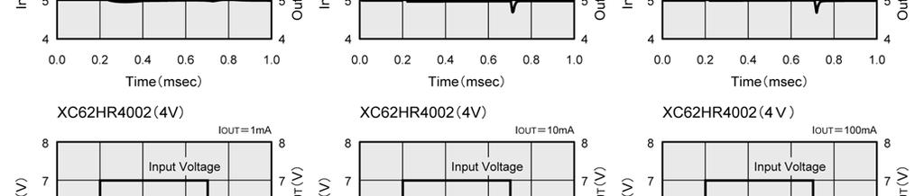
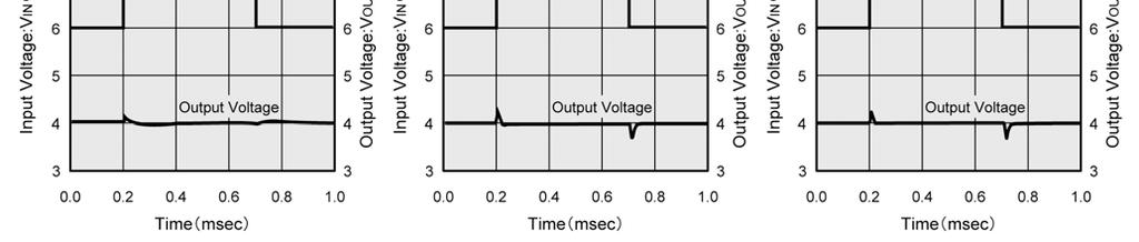
16 TYPICAL PERFORMANCE CHARACTERISTICS (Continued) (8) Input Transient Response 1 (Continued) (9) Input Transient Response 2 16/23

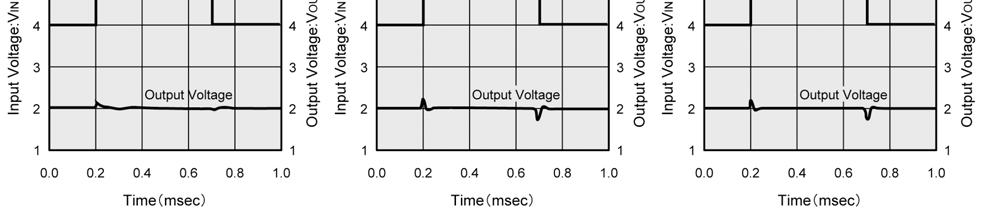
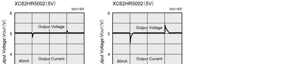
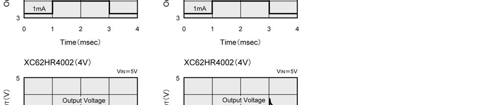
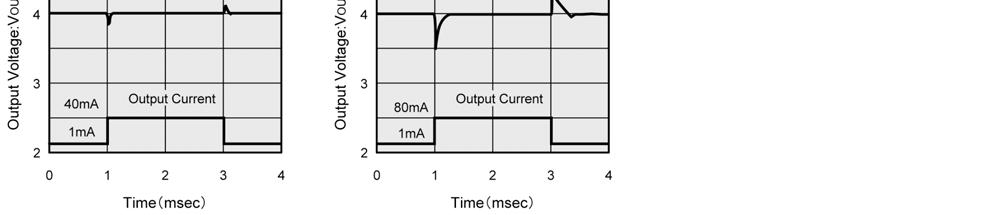
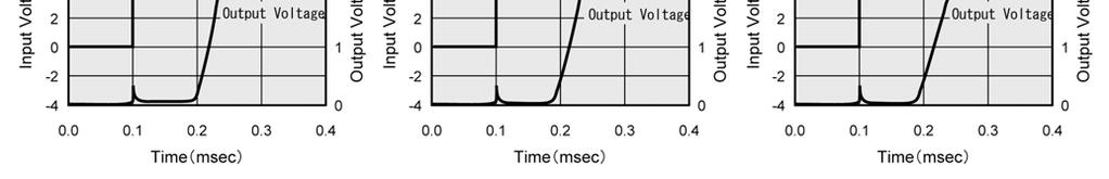
17 XC62H Series TYPICAL PERFORMANCE CHARACTERISTICS (Continued) (9) Input Transient Response 2 (Continued) (10) Load Transient Response Time (ms) Time (ms) Time (ms) Time (ms) 17/23


 Time (ms)")

18 TYPICAL PERFORMANCE CHARACTERISTICS (Continued) (10) Load Transient Response (Continued) Time (ms) Time (ms) Time (ms) (11) CE Pin Transient Response Time (ms) 18/23


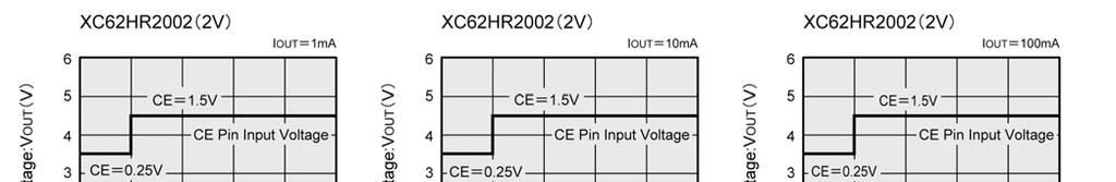
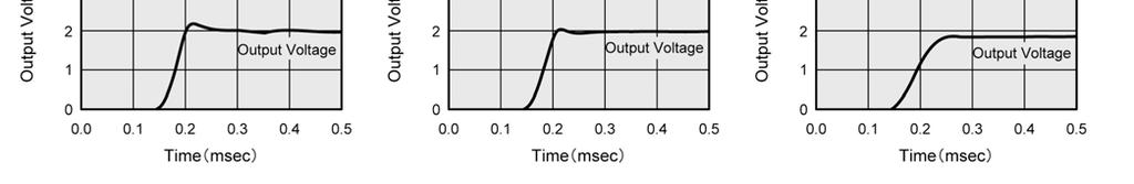
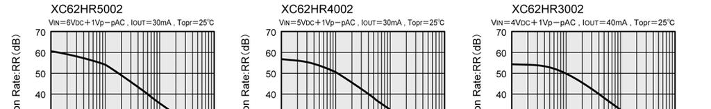

19 XC62H Series TYPICAL PERFORMANCE CHARACTERISTICS (Continued) (11) CE Pin Transient Response (Continued) (12) Ripple Rejection Rate 19/23
20 PACKAGING INFORMATION SOT-25 SOT-89-5 (0.1) 0.8 MIN 1.5± ±0.1 (0.3) (1.8) (0.4) (0.4) 4.35 MAX 0.8 MIN USP-6B 20/23
21 XC62H Series PACKAGING INFORMATION (Continued) USP-6B Reference Pattern Layout USP-6B Reference metal mask design MARKING RULE SOT-25, SOT represents integer of the output voltage MARK VOLTAGE (V) SOT (TOP VIEW) SOT-89-5 (TOP VIEW) 2 represents decimal number of the output voltage MARK VOLTAGE (V) represents temperature characteristics MARK - 4 represents production lot number 0 to 9, A to Z repeated, reverse character 0 to 9, A to Z repeated (G, I, J, O, Q, W excluded) 21/23
 PRODUCT SERIES 3 3 3.3 XC62HR330*D* 5 0 5.")
22 MARKING RULE USP-6B 1 represents product series MARK H PRODUCT SERIES XC62HR**0*D* 2 represents CE pin logic MARK LOGIC PRODUCT SERIES R Positive XC62HR**0*D* USP-6B (TOP VIEW) 34 represents output voltage ex: MARK 3 4 VOLTAGE(V) PRODUCT SERIES XC62HR330*D* XC62HR500*D* 5 represents temperature characteristics MARK TEMPERATURE CHARACTERISTICS PRODUCT SERIES 0 TYP±100ppm XC62HR**0*** 6 represents production lot number 0 to 9, A to Z repeated (G, I, J, O, Q, W excluded) Note: No character inversion used. 22/23
23 XC62H Series 1. The products and product specifications contained herein are subject to change without notice to improve performance characteristics. Consult us, or our representatives before use, to confirm that the information in this datasheet is up to date. 2. We assume no responsibility for any infringement of patents, patent rights, or other rights arising from the use of any information and circuitry in this datasheet. 3. Please ensure suitable shipping controls (including fail-safe designs and aging protection) are in force for equipment employing products listed in this datasheet. 4. The products in this datasheet are not developed, designed, or approved for use with such equipment whose failure of malfunction can be reasonably expected to directly endanger the life of, or cause significant injury to, the user. (e.g. Atomic energy; aerospace; transport; combustion and associated safety equipment thereof.) 5. Please use the products listed in this datasheet within the specified ranges. Should you wish to use the products under conditions exceeding the specifications, please consult us or our representatives. 6. We assume no responsibility for damage or loss due to abnormal use. 7. All rights reserved. No part of this datasheet may be copied or reproduced without the prior permission of TOREX SEMICONDUCTOR LTD. 23/23
XC62K Series GENERAL DESCRIPTION APPLICATIONS FEATURES TYPICAL PERFORMANCE CHARACTERISTICS TYPICAL APPLICATION CIRCUIT. Negative Voltage Regulators
 ETR0313_005 Negative Voltage Regulators GENERAL DESCRIPTION The XC62K series are highly precise, low power consumption, negative voltage regulators, manufactured using CMOS and laser trimming technologies.
XC62K Series GENERAL DESCRIPTION APPLICATIONS FEATURES TYPICAL PERFORMANCE CHARACTERISTICS TYPICAL APPLICATION CIRCUIT. Negative Voltage Regulators
 ETR0313_006 Negative Voltage Regulators GENERAL DESCRIPTION The XC62K series are highly precise, low power consumption, negative voltage regulators, manufactured using CMOS and laser trimming technologies.
High Speed LDO Regulators Low ESR Cap.Compatible,Output ON/OFFControl
 ETR0306_006 High Speed LDO Regulators Low ESR Cap.Compatible,Output ON/OFFControl GENERAL DESCRIPTION The XC6209/XC6212 series are highly precise, low noise, positive voltage LDO regulators manufactured
XC6210 Series APPLICATIONS. TYPICAL PERFORMANCE CHARACTERISTICS Dropout Voltage vs. Output Current TYPICAL APPLICATION CIRCUIT
 ETR317_6 High Current, High Speed LDO Regulators GENERAL DESCRIPTION The XC621 series are precise, low noise, high current, positive voltage low dropout regulators. They are fabricated using Torex s CMOS
200mA High Speed LDO Voltage Regulator with Inrush Current Prevention
 ETR03066-004 200mA High Speed LDO Voltage Regulator with Inrush Current Prevention GENERAL DESCRIPTION The XC6233 series is a 200mA high speed LDO regulator that features high accurate high ripple rejection
XC6201 Series GENERAL DESCRIPTION FEATURES APPLICATIONS TYPICAL PERFORMANCE CHARACTERISTICS TYPICAL APPLICATION CIRCUIT. Positive Voltage Regulators
 ETR0301_004 Positive Voltage Regulators GENERAL DESCRIPTION The XC6201 series are highly precise, low power consumption, positive voltage regulators manufactured using CMOS and laser trimming technologies.
XC6210 Series APPLICATIONS. TYPICAL PERFORMANCE CHARACTERISTICS Dropout Voltage vs. Output Current TYPICAL APPLICATION CIRCUIT
 ETR0317_004 High Current, High Speed LDO Regulators GENERAL DESCRIPTION The XC6210 series are precise, low noise, high current, positive voltage low dropout regulators. They are fabricated using Torex
XC6214 Series. FEATURES Maximum Output Current APPLICATIONS. TYPICAL PERFORMANCE CHARACTERISTICS Dropout Voltage vs. Output Current XC6214P332
 XC6 Series ETR8_ ma Output Current, High Speed LDO Regulators, Thermal Shutdown Function, Ceramic Capacitor Compatible GENERAL DESCRIPTION The XC6 series are highly precise, low noise, high current, positive
High Speed LDO Regulators Low ESR Cap.Compatible,Output ON/OFFControl
 ETR0306_005 High Speed LDO Regulators Low ESR Cap.Compatible,Output ON/OFFControl GENERAL DESCRIPTION The XC6209/XC6212 series are highly precise, low noise, positive voltage LDO regulators manufactured
XC6401 Series FEATURES
 XC1 Series ETR9_7 Dual LDO Regulators, Low ESR Cap. Compatible GENERAL DESCRIPTION The XC1 series are highly accurate, Dual, low noise, CMOS LDO voltage regulators. Performance features of the series includes
FEATURES Maximum Output Current APPLICATIONS. TYPICAL PERFORMANCE CHARACTERISTICS Supply Current vs. Input Voltage TYPICAL APPLICATION CIRCUIT 1/22
 ETR0329-005 GENERAL DESCRIPTION XC6218 series are highly precise, low noise, positive voltage LDO regulators manufactured using CMOS processes. The series achieves very low supply current, 1.0A (TYP.)
XC6234 Series APPLICATIONS TYPICAL APPLICATION CIRCUIT TYPICAL PERFORMANCE CHARACTERISTICS. 200mA High Speed LDO Regulator with ON/OFF Switch 1/23
 ETR367-2 ma High Speed LDO Regulator with ON/OFF Switch GENERAL DESCRIPTION The series is a ma high speed LDO regulator that features high accurate, high ripple rejection and low dropout. The series consists
XC6206 Series GENERAL DESCRIPTION FEATURES APPLICATIONS TYPICAL PERFORMANCE CHARACTERISTICS TYPICAL APPLICATION CIRCUIT 1/17
 ETR0305_004a GENERAL DESCRIPTION The XC6206 series are highly precise, low power consumption, 3 terminal, positive voltage regulators manufactured using CMOS and laser trimming technologies. The series
GENERAL DESCRIPTION FEATURES APPLICATIONS TYPICAL PERFORMANCE CHARACTERISTICS TYPICAL APPLICATION CIRCUIT 1/17. Battery powered equipment
 ETR0305_003a GENERAL DESCRIPTION The XC6206 series are highly precise, low power consumption, high voltage, positive voltage regulators manufactured using CMOS and laser trimming technologies. The series
APPLICATIONS. FEATURES Maximum Output Current : 200mA (300mA Limit, TYP.)
") Low Power Consumption:.8µA (TYP.) Range :.V ~.V Range :.9V ~.V Maximum Output Current: ma (ma Limit, TYP.) @ VOUT=.V, VIN=.V Current Limiter Circuit Built-In Ceramic Capacitor Compatible Small Packages
Low Power Consumption:.8µA (TYP.) Range :.V ~.V Range :.9V ~.V Maximum Output Current: ma (ma Limit, TYP.) @ VOUT=.V, VIN=.V Current Limiter Circuit Built-In Ceramic Capacitor Compatible Small Packages
XC6401 Series FEATURES. TYPICAL PERFORMANCE CHARACTERISTICS Interactive Load Transient Response TYPICAL APPLICATION CIRCUITS
 XC Series ETR9_ Dual LDO Regulators, Low ESR Cap. Compatible GENERAL DESCRIPTION The XC series are highly accurate, Dual, low noise, CMOS LDO voltage regulators. Performance features of the series includes
APPLICATIONS Mobile Phones Cordless phones and radio communication equipment Portable games Cameras, Video recorders Portable Audio Equipment PDAs
 Low Power Consumption : μa (TYP.) Dropout Voltage : mv @ ma : mv @ma Range :.8V to.v Output Current : More than ma (ma limit) Low Output Noise High Ripple Rejection Rate Low ESR capacitor compatible GENERAL
300mA/150mA High Speed LDO Regulators with ON-OFF Control
 ETR03004-010 300mA/150mA High Speed LDO Regulators with ON-OFF Control GENERAL DESCRIPTION The XC6204/XC6205 series are highly precise, low noise, positive voltage LDO regulators manufactured using CMOS
XC6206 Series GENERAL DESCRIPTION FEATURES APPLICATIONS TYPICAL PERFORMANCE CHARACTERISTICS TYPICAL APPLICATION CIRCUIT 1/17
 ETR0305_007 GENERAL DESCRIPTION The XC6206 series are highly precise, low power consumption, 3 terminal, positive voltage regulators manufactured using CMOS and laser trimming technologies. The series
GENERAL DESCRIPTION FEATURES APPLICATIONS TYPICAL PERFORMANCE CHARACTERISTICS TYPICAL APPLICATION CIRCUIT 1/17
 ETR0305_002 GENERAL DESCRIPTION The XC6206 series are highly precise, low power consumption, high voltage, positive voltage regulators manufactured using CMOS and laser trimming technologies. The series
XC6202 Series GENERAL DESCRIPTION APPLICATIONS. FEATURES Maximum Output Current : 150mA (within Pd) Maximum Operational Voltage : 20V
 Maximum Operational Voltage : 20V") XC6 Series High Voltage Positive Voltage Regulators ETR3_7 GENERAL DESCRIPTION The XC6 series are highly precise, low power consumption, high voltage input, positive voltage regulators manufactured using
XC6 Series High Voltage Positive Voltage Regulators ETR3_7 GENERAL DESCRIPTION The XC6 series are highly precise, low power consumption, high voltage input, positive voltage regulators manufactured using
28 V Input High Speed Voltage Regulator
 28 V Input High Speed Voltage Regulator FEATURES Operating Voltage Range 2.0 V 28.0 V Output Voltage Range from 1.8 V to 18.0 V with 0.1 V increments Output Voltage Accuracy ± 2% Temperature Stability
APPLICATIONS Mobile phones Cordless phones Cameras, video recorders Portable games Portable AV equipment Reference voltage Battery powered equipment
 CMOS Low Power Consumption Dropout Voltage : 60mV @ 30mA 200mV @ 100mA Maximum Output Current : 150mA (300mA=XC6204 E to H Type) Highly Accurate : ±2% Output Voltage Range : 1.8V ~ 6.0V (XC6204) 0.9V ~
XB1086 Series GENERAL DESCRIPTION FEATURES APPLICATIONS TYPICAL APPLICATION CIRCUITS TYPICAL PERFORMANCE CHARACTERISTICS
 XB086 Series ETR0325-008.5A Positive Voltage Regulator GENERAL DESCRIPTION The XB086 is a series of low dropout positive voltage regulators with a high output current capability of.5a. Stable output can
XB1085 Series GENERAL DESCRIPTION FEATURES APPLICATIONS. TYPICAL PERFORMANCE CHARACTERISTICS Output Voltage vs. Output Current
 XB085 Series ETR0324-008 3.0A Positive Voltage Regulator GENERAL DESCRIPTION The XB085 is a series of low dropout positive voltage regulators with a high output current capacity of 3.0A. Stable output
28 V, 150 ma Voltage Regulator with Stand-by Mode
 28 V, 150 ma Voltage Regulator with Stand-by Mode FEATURES Operating Voltage Range 2.0 V 28.0 V Output Voltage Range from 2.0 V to 12.0 V with 0.1 V increments (B series) or 2.0 V 23 V with external resistors
XC61F Series GENERAL DESCRIPTION APPLICATIONS
 ETR0202-007a Voltage Detectors, Delay Circuit Built-In GENERAL DESCRIPTION The XC61F series are highly accurate, low power consumption voltage detectors, manufactured using CMOS and laser trimming technologies.
PIN CONFIGURATION *The dissipation pad for the USP-6B package should be solder-plated in recommended mount pattern and metal masking so as to enhance
 ETR0305_004a GENERAL DESCRIPTION The XC6206 series are highly precise, low power consumption, 3 terminal, positive voltage regulators manufactured using CMOS and laser trimming technologies. The series
XC8102 Series FEATURES APPLICATIONS TYPICAL PERFORMANCE CHARACTERISTICS TYPICAL APPLICATION CIRCUIT
 ETR2502-012 Load Switch with Low On-Resistance (Current Limit 400mA) GENERAL DESCRIPTION The XC8102 series is a low ON resistance load switch IC with ON/OFF control and output current protection which
XC6504 Series. APPLICATIONS Mobile devices / terminals Wireless LAN Modules (wireless, cameras, etc.) TYPICAL PERFORMANCE CHARACTERISTICS
 TYPICAL PERFORMANCE CHARACTERISTICS") XC654 Series ETR47-7.6μA Ultra Low Power Consumption Small Voltage Regulator (CL Capacitor-Less) GENERAL DESCRIPTION The XC654 series is a highly accurate CMOS voltage regulator that achieves very low
XC654 Series ETR47-7.6μA Ultra Low Power Consumption Small Voltage Regulator (CL Capacitor-Less) GENERAL DESCRIPTION The XC654 series is a highly accurate CMOS voltage regulator that achieves very low
Highly Accurate, Ultra Small, Low Power Consumption Voltage Detector
 ETR0209-004 Highly Accurate, Ultra Small, Low Power Consumption Voltage Detector GENERAL DESCRIPTION The XC6120 series are highly precise, low power consumption voltage detectors, manufactured using CMOS
XC6119 Series. FEATURES High Accuracy : +2% APPLICATIONS TYPICAL PERFORMANCE CHARACTERISTICS TYPICAL APPLICATION CIRCUIT
 XC69 Series ETR0206-00 Voltage Detector with Delay Time Adjustable GENERAL DESCRIPTION The XC69 series is a highly precise, low power consumption voltage detector, manufactured using CMOS and laser trimming
Built-in Inrush Current Protection, 300mA High Speed LDO Voltage Regulator
 XC6223 Series ETR339-5 Built-in Inrush Current Protection, 3mA High Speed LDO Voltage Regulator GENERAL DESCRIPTION The XC6223 series is a high speed LDO regulator that features high accurate, low noise,
XCM410 Series. FEATURES High Accuracy APPLICATIONS TYPICAL APPLICATION CIRCUIT. 2 Channel Voltage Detector (Sense Pin separated from V DD ) 1/13
 1/13") ETR2426_003 2 Channel Voltage Detector (Sense Pin separated from V DD ) GENERAL DESCRIPTION The XCM410 series is a multi combination module IC which comprises of two voltage detectors, XC6108 and XC6109
ETR2426_003 2 Channel Voltage Detector (Sense Pin separated from V DD ) GENERAL DESCRIPTION The XCM410 series is a multi combination module IC which comprises of two voltage detectors, XC6108 and XC6109
XC61C Series GENERAL DESCRIPTION
 ETR1_16 Low Voltage Detectors (VDF=.8V~1.V) Standard Voltage Detectors (VDF 1.6V~6.V) GENERAL DESCRIPTION The XC61C series are highly precise, low power consumption voltage detectors, manufactured using
High Current, High Speed LDO Regulators, Voltage Detector Function
 ETR1004-006 High Current, High Speed LDO Regulators, Voltage Detector Function GENERAL DESCRIPTION The XC6413/XC6414 series are highly precise, low noise, positive voltage LDO regulators with voltage detector
XB1117 Series APPLICATIONS. FEATURES Maximum Output Current TYPICAL PERFORMANCE CHARACTERISTICS TYPICAL APPLICATION CIRCUIT
 ETR0315_006 1A Low Dropout Positive oltage Regulator GENERAL DESCRIPTION The XB1117 series is 1A Bi-polar transistor LDO voltage regulator. Output voltage of the XB1117P series is fixed to 1.8, 2.5, 3.3,
XC6215 Series FEATURES APPLICATIONS TYPICAL APPLICATION CIRCUIT TYPICAL PERFORMANCE CHARACTERISTICS
 XC Series ETR9_.8μA Low Power Consumption Voltage Regulator with ON/OFF Switch GENERAL DESCRIPTION The XC series are highly precise, low noise, positive voltage LDO regulators manufactured using CMOS processes.
XC9253R Series TYPICAL APPLICATION CIRCUIT. Synchronous Step-Down DC/DC Converter 1/13. GreenOperation Compatible
 ETR0528_003 Synchronous Step-Down DC/DC Converter GreenOperation Compatible GENERAL DESCRIPTION The series is a group of synchronous-rectification type DC/DC converters with a built-in 0.6P-channel driver
600mA Driver Tr. Built-In, Synchronous Step-Down DC/DC Converter
 XC9254R Series ETR0529-003 600mA Driver Tr. Built-In, Synchronous Step-Down DC/DC Converter GreenOperation Compatible GENERAL DESCRIPTION The XC9254R series is a group of synchronous-rectification type
PWM,PWM/PFM Switching Step-Up & Down DC/DC Converter Controller ICs
 ETR0601_001c PWM,PWM/PFM Switching Step-Up & Down DC/DC Converter Controller ICs GENERAL DESCRIPTION Green Operation Compatible The XC9301/XC9302 series are step-up/down DC/DC converter controller ICs
XC6901 Series APPLICATIONS TYPICAL PERFORMANCE CHARACTERISTICS TYPICAL APPLICATION CIRCUIT. 200mA Negative Voltage Regulator with ON/OFF Control 1/28
 ETR343-6 2mA Negative Voltage Regulator with ON/OFF Control GENERAL DESCRIPTION The is a negative voltage CMOS regulator which includes a reference voltage source, error amplifier, driver transistor, current
XC6901 Series APPLICATIONS TYPICAL PERFORMANCE CHARACTERISTICS TYPICAL APPLICATION CIRCUIT. 200mA Negative Voltage Regulator with ON/OFF Control 1/28
 XC691 Series ETR343-7 2mA Negative Voltage Regulator with ON/OFF Control GENERAL DESCRIPTION The XC691 Series is a negative voltage CMOS regulator which includes a reference voltage source, error amplifier,
Ultra Small Analog Output Temperature Sensor with Alarm Output Pin
 ETR0902-005 Ultra Small Analog Output Temperature Sensor with Alarm Output Pin GENERAL DESCRIPTION The XC3101 series is a temperature sensor IC which features ultra small, low current consumption, and
High Speed Low Dropout Middle Current Voltage Regulators. Designator Symbol Description Designator Symbol Description CE Pin Logic :
 High Speed Low Dropout Middle Current Voltage Regulators General Description The series are highly precise, low noise, positive voltage LDO regulators manufactured using CMOS processes. The series achieves
XC2163 Series GENERAL DESCRIPTION APPLICATIONS FEATURES PIN ASSIGNMENT PIN CONFIGURATION /INH, Q0 PIN FUNCTION
 ETR1403_001a ICs for use with 3rd Overtone Crystal Oscillators GENERAL DESCRIPTION The XC2163 series are high frequency, low current consumption CMOS ICs with built-in crystal oscillator and divider circuits.
XC9801/XC9802 Series GENERAL DESCRIPTION FEATURES APPLICATIONS TYPICAL APPLICATION CIRCUIT TYPICAL PERFORMANCE CHARACTERISTICS
 XC9801/XC9802 Series ETR0804-006 Regulated Voltage Step-Up Charge Pump ICs GENERAL DESCRIPTION The XC9801 series are fixed regulated voltage step-up charge pump ICs which provide stable, highly efficient,
Ultra Small, Low Power Consumption Voltage Detector
 Ultra Small, Low Power Consumption Voltage Detector FEATURES Accuracy ± 2% at V DF 1.5 V or ±0.03 V Low Power Consumption at 0.6 μa typical at V DF = 2.7 V, V IN = 2.97 V Detect Voltage Range 0.7 V 5.0
XC2300 Series GENERAL DESCRIPTION APPLICATIONS FEATURES PIN CONFIGURATION PIN ASSIGNMENT /INH, Q0 PIN FUNCTION. Tri-State Buffer ICs 1/7
 ETR1406_001a Tri-State Buffer ICs GENERAL DESCRIPTION The 2300 Series are a group of high frequency, CMOS low power tri-state buffer ICs with input amplifier, divider and output tri-state buffer circuits
Dual LDO Regulator (ch1: 300mA, ch2: 100mA) with ON/OFF Switch
 with ON/OFF Switch") XC6419 Series ETR338-5 Dual LDO Regulator (ch1: 3mA, ch2: 1mA) with ON/OFF Switch GENERAL DESCRIPTION The XC6419 series is a dual CMOS LDO regulator. The series features high accuracy, low output noise,
XC6419 Series ETR338-5 Dual LDO Regulator (ch1: 3mA, ch2: 1mA) with ON/OFF Switch GENERAL DESCRIPTION The XC6419 series is a dual CMOS LDO regulator. The series features high accuracy, low output noise,
XC6602 Series. APPLICATIONS Smart phones / Mobile phones. FEATURES Maximum Output Current : 1A (1.3A Limit)
") XC66 Series ETR35 A,.5V Low Input Voltage, High Speed LDO Regulator GENERAL DESCRIPTION The XC66 series is a low voltage input (.5V) operation and provides high accuracy ±5mV/±mV and can supply large current
XC66 Series ETR35 A,.5V Low Input Voltage, High Speed LDO Regulator GENERAL DESCRIPTION The XC66 series is a low voltage input (.5V) operation and provides high accuracy ±5mV/±mV and can supply large current
A6304A. AiT Semiconductor Inc. APPLICATION ORDERING INFORMATION TYPICAL APPLICATION
 DESCRIPTION The series are highly precise, low noise, positive voltage LDO regulators manufactured using CMOS processes. The series achieves high ripple rejection and low dropout and consists of a standard
PWM Controlled, PWM/PFM Switchable Step-up DC/DC Controllers
 XC6367/XC6368 Series ETR0401_005 PWM Controlled, PWM/PFM Switchable Step-up DC/DC Controllers GreenOperation-Compatible GENERAL DESCRIPTION The XC6367/XC6368 series are multi-functional step-up DC/DC controllers
XP151A13A0MR-G GENERAL DESCRIPTION
 ETR1119_003 Power MOSFET GENERAL DESCRIPTION The XP151A13A0MR-G is an N-channel Power MOSFET with low on state resistance and ultra high-speed switching characteristics. Because high-speed switching is
XP162A11C0PR-G GENERAL DESCRIPTION
 ETR1125_003 Power MOSFET GENERAL DESCRIPTION The XP162A11C0PR-G is a P-channel Power MOSFET with low on-state resistance and ultra high-speed switching characteristics. Because high-speed switching is
XP152A11E5MR-G GENERAL DESCRIPTION
 ETR1120_003 Power MOSFET GENERAL DESCRIPTION The XP152A11E5MR-G is a P-channel Power MOSFET with low on-state resistance and ultra high-speed switching characteristics. Because high-speed switching is
XP161A1355PR-G GENERAL DESCRIPTION. FEATURES Low On-State Resistance : Rds (on)= Vgs = 4.5V APPLICATIONS PRODUCT NAME
= Vgs = 4.5V APPLICATIONS PRODUCT NAME") ETR1124_003 Power MOSFET GENERAL DESCRIPTION The XP161A1355PR-G is an N-channel Power MOSFET with low on-state resistance and ultra high-speed switching characteristics. Because high-speed switching is
ETR1124_003 Power MOSFET GENERAL DESCRIPTION The XP161A1355PR-G is an N-channel Power MOSFET with low on-state resistance and ultra high-speed switching characteristics. Because high-speed switching is
PT7M8205 LDO Regulator
 Features Output Current: 300mA or more Dropout Voltage: 270mV @ 300mA for 3.3V Operating Voltage Range: 1.8 to 5.5V Output Voltage Range: 1.2 to 3.3V (100mV Step) Low Power Consumption: 65µA High Ripple
LN809. Voltage Detectors With Delay Circuit Built-In. General Description. Applications. Features. Ordering Information
 Voltage Detectors With Delay Circuit Built-In General Description The is a cost-effective system supervisor Integrated Circuit (IC) designed to monitor VCC in digital and mixed signal systems and provide
XC9119D10A Series APPLICATIONS TYPICAL APPLICATION CIRCUIT. TYPICAL PERFORMANCE CHARACTERISTICS Efficiency vs. Output Current
 XC9119D1A Series ETR48_9 1MHz, PWM Controlled, Step-Up DC/DC Converter, Ceramic Capacitor Compatible GENERAL DESCRIPTION The XC9119D1A series is 1MHz, PWM controlled step-up DC/DC converter, designed to
Synchronous Step-Up PFM DC/DC Converter
 Synchronous Step-Up PFM DC/DC Converter FEATURES Operating Input Voltage Range: 0.9 V ~ 5.5 V Output Voltage Range: 1.8 V~5.0 V with (0.1 V increments, accuracy ± 2.0%) Built-in Switching NMOSFET (0.6
HIGH RIPPLE-REJECTION LOW DROPOUT LOW INPUT-AND-OUTPUT CAPACITANCE CMOS VOLTAGE REGULATOR
 Rev.3.2_ HIGH RIPPLE-REJECTION LOW DROPOUT LOW INPUT-AND-OUTPUT CAPACITANCE CMOS VOLTAGE REGULATOR S-12 Series The S-12 Series is a positive voltage regulator with a low dropout voltage, high output voltage
16V Input Voltage Step-Down DC/DC Controller
 16V Input Voltage Step-Down DC/DC Controller FEATURES Operating Input Voltage Range: 2.8V ~ 16.0V Output Voltage Range Externally Set: > 1.2V Output Current: up to 3A Reference Voltage: 0.9V ± 1.5% Oscillation
VRR Series. AnaSem. High speed, Low dropout, ±1% High output accuracy CMOS Voltage Regulator with On/Off circuit. Analog Semiconductor IC. AnaSem Inc.
 AnaSem Analog Semiconductor IC High speed, Low dropout, ±% High output accuracy CMOS Voltage Regulator with On/Off circuit Rev. E9- Rev. E9- AnaSem Products Data Sheet Analog Semiconductor IC High speed,
I/O Name Descriptions
 Features Output Current: 300mA or more Dropout Voltage: 270mV @ 300mA for 3.3V Operating Voltage Range: 1.8V to 5.5V Output Voltage Range: 1.2V to 3.3V (100mV Step) Low Power Consumption: 65 A Standby
*1. Attention should be paid to the power dissipation of the package when the load is large. *2. Refer to Product Name Structure for details.
 www.sii-ic.com HIGH RIPPLE-REJECTION AND LOW DROPOUT CMOS VOLTAGE REGULATOR Seiko Instruments Inc., 21-21 Rev.5._ The S-L298 series is a positive voltage regulator with a low dropout voltage, high output
*1. Attention should be paid to the power dissipation of the package when the load is large.
 Rev.3._ HIGH RIPPLE-REJECTION LOW DROPOUT CMOS VOLTAGE REGULATOR Features The S-L298 series is a positive voltage regulator with a low dropout voltage, high output voltage accuracy, and low current consumption
XC9110/XC9111 Series GENERAL DESCRIPTION APPLICATIONS FEATURES TYPICAL APPLICATION CIRCUIT. PFM Controlled Step-Up DC/DC Converter / Controller ICs
 XC911/XC9111 Series ETR46-6a PFM Controlled Step-Up DC/DC Converter / Controller ICs GENERAL DESCRIPTION The XC911/9111 series is a group of PFM controlled step-up DC/DC converter/controller ICs designed
XP202A0003MR-G FEATURES APPLICATIONS PRODUCT NAME PIN CONFIGURATION ABSOLUTE MAXIMUM RATINGS ELECTRICAL CHARACTERISTICS. P-channel 4V (G-S) MOSFET 1/5
 MOSFET 1/5") -G ETR28 P-channel 4V (G-S) MOSFET FEATURES Low On Resistance Ultra High Speed Switching V Driving EU RoHS Compliant, Pb Free ABSOLUTE MAXIMUM RATINGS APPLICATIONS Switching PRODUCT NAME PRODUCT NAME PACKAGE
-G ETR28 P-channel 4V (G-S) MOSFET FEATURES Low On Resistance Ultra High Speed Switching V Driving EU RoHS Compliant, Pb Free ABSOLUTE MAXIMUM RATINGS APPLICATIONS Switching PRODUCT NAME PRODUCT NAME PACKAGE
PT7M8205 LDO Regulator
 PT7M8205 Features Output Current: 300mA or more Dropout Voltage: 270mV @ 300mA for 3.3V Operating Voltage Range: 1.8 to 5.5V Output Voltage Range: 1.2 to 3.3V (100mV Step) Low Power Consumption: 65A High
HIGH RIPPLE-REJECTION LOW DROPOUT MIDDLE OUTPUT CURRENT CMOS VOLTAGE REGULATOR
 Rev.2.3_ HIGH RIPPLE-REJECTION LOW DROPOUT MIDDLE OUTPUT CURRENT CMOS VOLTAGE REGULATOR S-1131 Series The S-1131 Series is a positive voltage regulator with a low dropout voltage, high output voltage accuracy,
VRH Series. AnaSem. High speed, Low dropout, ±1% High output accuracy CMOS Voltage Regulator with On/Off circuit. Analog Semiconductor IC.
 安纳森 Analog Semiconductor IC High speed, Low dropout, ±% High output accuracy CMOS Voltage Regulator with On/Off circuit (IMPORTANT: Please check the last page for Genuine Product Labeling) Rev. E- Website:
1.5 V to 5.5 V, selectable in 0.1 V step Output voltage accuracy: ±1.0% Dropout voltage:
 www.sii-ic.com HIGH RIPPLE-REJECTION LOW DROPOUT CMOS VOLTAGE REGULATOR Seiko Instruments Inc., 22-215 Rev.5.1_ The is a positive voltage regulator with a low dropout voltage, high-accuracy output voltage,
300mA Low Dropout Programmable output CMOS Voltage Regulators. Designator Symbol Description Designator Symbol Description CE Pin Logic :
 300mA Low Dropout Programmable output CMOS Voltage Regulators General Description The series are highly precise, low noise, positive voltage LDO regulators manufactured using CMOS processes. The series
1.5 V to 5.5 V, selectable in 0.1 V step Output voltage accuracy:
 www.ablicinc.com HIGH RIPPLE-REJECTION LOW DROPOUT CMOS VOLTAGE REGULATOR ABLIC Inc., 23-215 Rev.3.1_2 The is a positive voltage regulator with a low dropout voltage, high-accuracy output voltage, and
S-L2980 Series HIGH RIPPLE-REJECTION AND LOW DROPOUT CMOS VOLTAGE REGULATOR. Features. Applications. Package
 www.ablicinc.com HIGH RIPPLE-REJECTION AND LOW DROPOUT CMOS VOLTAGE REGULATOR ABLIC Inc., 21-212 Rev.5.1_2 The is a positive voltage regulator with a low dropout voltage, high output voltage accuracy,
PT7M8206 LDO Regulator
 Features Output Current: 300mA or more Dropout Voltage: 270mV @ 300mA for 3.3V Operating Voltage Range: 1.8 to 5.5V Output Voltage Range: 1.2 to 3.3V (100mV Step) Low Power Consumption: 65µA Standby Current:
High Ripple-Rejection Low Dropout CMOS Voltage Regulator
 High Ripple-Rejection Low Dropout CMOS Voltage Regulator General Description The Series is a positive voltage regulator with a low dropout voltage, high output voltage accuracy, and low current consumption
1.5 V to 5.5 V, selectable in 0.1 V step Output voltage accuracy: 140 mv typ. (3.0 V output product, I OUT = 200 ma)
") S-1165 Series www.ablicinc.com HIGH RIPPLE-REJECTION LOW DROPOUT CMOS VOLTAGE REGULATOR ABLIC Inc., -15 Rev.4.1_ The S-1165 Series is a positive voltage regulator with a low dropout voltage, high-accuracy
S-1165 Series www.ablicinc.com HIGH RIPPLE-REJECTION LOW DROPOUT CMOS VOLTAGE REGULATOR ABLIC Inc., -15 Rev.4.1_ The S-1165 Series is a positive voltage regulator with a low dropout voltage, high-accuracy
VRD Series. AnaSem. High speed, Low dropout, ±1% High output accuracy CMOS Voltage Regulator with Dual output. Analog Semiconductor IC.
 安纳森 Analog Semiconductor IC High speed, Low dropout, ±% High output accuracy CMOS Voltage Regulator with Dual output (IMPORTANT: Please check the last page for Genuine Product Labeling) Rev. E- Website:
LOW ESR Cap. Compatible Positive Voltage Regulators XC6206 Series
 SOT-23 Unit: mm Features Maximum Output Current : 200mA Dropout Voltage : 250mV (IOUT = 100mA) Maximum Operating Voltage : 6V Output Voltage Range : 1.2V ~ 5V (0.1V increments) Highly Accurate : ±2%@VOUT
1.5 V to 5.5 V, selectable in 0.1 V step
 S-1167 Series www.ablicinc.com ULTRA LOW CURRENT CONSUMPTION, HIGH RIPPLE REJECTION AND LOW DROPOUT CMOS VOLTAGE REGULATOR ABLIC Inc., 24-215 Rev.3.2_2 The S-1167 Series is a positive voltage regulator
SOT-23-5, 5-Pin SON(A) *1. Attention should be paid to the power dissipation of the package when the output current is large.
 *1. Attention should be paid to the power dissipation of the package when the output current is large.") Rev.2.2_ HIGH RIPPLE-REJECTION LOW DROPOUT CMOS VOLTAGE REGULATOR The is a positive voltage regulator with a low dropout voltage, high output voltage accuracy, and low current consumption developed based
Rev.2.2_ HIGH RIPPLE-REJECTION LOW DROPOUT CMOS VOLTAGE REGULATOR The is a positive voltage regulator with a low dropout voltage, high output voltage accuracy, and low current consumption developed based
Ultra Low Quiescent Current Synchronous Step-Down PFM DC/DC Converter for Low Output Voltage
 XC9272 Series ETR05057-001 Ultra Low Quiescent Current Synchronous Step-Down PFM DC/DC Converter for Low Output Voltage GENERAL DESCRIPTION XC9272 series are Ultra Low Quiescent Current synchronous-rectification
1A Driver Transistor Built-In, Multi Functional Step-Up DC/DC Converters
 ETR0412-010 1A Driver Transistor Built-In, Multi Functional Step-Up DC/DC Converters GreenOperation Compatible GENERAL DESCRIPTION XC9131 series are synchronous step-up DC/DC converterswith a 0.2(TYP.)
ACE507A. Precise Low Dropout Voltage Regulator. Description. Features. Application. Functional Block Diagram
 Description The series are precise, low power consumption; positive voltage regulators manufactured using CMOS and laser trimming technologies. The series provides large currents with a significantly small
28V Low Power Consumption 150mA Voltage Regulators (with Stand-by Function)
") XC/XE Series ETR_ V Low Power Consumption ma Voltage Regulators (with Stand-by Function) GENERAL DESCRIPTION XC/XE series are positive voltage regulator ICs with V of operation voltage. The series consists
XC/XE Series ETR_ V Low Power Consumption ma Voltage Regulators (with Stand-by Function) GENERAL DESCRIPTION XC/XE series are positive voltage regulator ICs with V of operation voltage. The series consists
1.5 V to 5.5 V, selectable in 0.1 V step Output voltage accuracy:
 S-117 Series www.ablicinc.com HIGH RIPPLE-REJECTION AND LOW DROPOUT HIGH OUTPUT CURRENT CMOS VOLTAGE REGULATOR ABLIC Inc., 23-215 Rev.4.1_2 The S-117 Series is a positive voltage regulator with a low dropout
XC8107 Series APPLICATIONS. FEATURES Input Voltage TYPICAL PERFORMANCE CHARACTERISTICS TYPICAL APPLICATION CIRCUIT. 85mΩ High Function Power Switch
 ETR33003-003 85mΩ High Function Power Switch GENERAL DESCRIPTION The XC8107 series is a P-channel MOSFET power switch IC with a low ON resistance. A current limit, reverse current prevention (prevents
HIGH RIPPLE-REJECTION LOW DROPOUT MIDDLE OUTPUT CURRENT CMOS VOLTAGE REGULATOR
 Rev.3._1 HIGH RIPPLE-REJECTION LOW DROPOUT MIDDLE OUTPUT CURRENT CMOS VOLTAGE REGULATOR S-1131 Series The S-1131 Series is a positive voltage regulator with a low dropout voltage, high output voltage accuracy,
S-1132 Series HIGH RIPPLE-REJECTION AND LOW DROPOUT MIDDLE OUTPUT CURRENT CMOS VOLTAGE REGULATOR. Features. Applications. Packages.
 S-1132 Series www.ablicinc.com HIGH RIPPLE-REJECTION AND LOW DROPOUT MIDDLE OUTPUT CURRENT CMOS VOLTAGE REGULATOR ABLIC Inc., 24-215 Rev.4.2_2 The S-1132 Series is a positive voltage regulator with a low
200mA Low Power Consumption CMOS LDO Regulator CLZ6821/22
 General Description The CLZ6821 is a positive LDO regulator designed on patent pending CMOS circuit technologies. The device attains high ripple rejection ratio and superior line and load transient response
PT7M mA, High PSRR, LDO Regulator Description. Features. Applications. Pin Assignment. Pin Description Pin No I/O Pin Name Description 1 I VIN
 Features Input Voltage Range:.7V to 5.5V 3mA Guaranteed Output Current Stable with.47f Ceramic Output Capacitors Low Dropout Voltage 5mV@5mA (Vout=2.8V) Low Quiescent Current 36A High PSRR 75dB@kHz Auto
Ultra-low Power Consumption LDO. CMOS Voltage Regulator With ON/OFF Switch
 Ultra-low Power Consumption LDO CMOS Voltage Regulator With ON/OFF Switch MD51XX Series 300mA MD51XX is a highly accurate low dropout voltage regulator (LDO) manufactured in CMOS processes. It can deliver
FEATURES Ultra-Low Power. High Accuracy. Temperature Characteristics Hysteresis width. Detect voltage range Operating voltage range Output type
 XC6136 Series Ultra-Low Power (88nA) Voltage Detector ETR242-1a GENERAL DESCRIPTION The XC6136 series is ultra-low power voltage detector with high accuracy detection, manufactured using CMOS process and
70 db typ. (1.0 V output product, f = 1.0 khz) Built-in overcurrent protection circuit: Limits overcurrent of output transistor.
 Built-in overcurrent protection circuit: Limits overcurrent of output transistor.") S-1155 Series www.ablicinc.com HIGH RIPPLE-REJECTION LOW DROPOUT HIGH OUTPUT CURRENT CMOS VOLTAGE REGULATOR ABLIC Inc., 7-15 Rev..1_3 The S-1155 Series, developed by using CMOS technology, is a positive
S-1155 Series www.ablicinc.com HIGH RIPPLE-REJECTION LOW DROPOUT HIGH OUTPUT CURRENT CMOS VOLTAGE REGULATOR ABLIC Inc., 7-15 Rev..1_3 The S-1155 Series, developed by using CMOS technology, is a positive
S-1142A/B Series HIGH-WITHSTAND VOLTAGE LOW CURRENT CONSUMPTION LOW DROPOUT CMOS VOLTAGE REGULATOR. Features. Application. Package.
 www.ablicinc.com HIGH-WITHSTAND VOLTAGE LOW CURRENT CONSUMPTION LOW DROPOUT CMOS VOLTAGE REGULATOR ABLIC Inc., 29-214 Rev.4.2_2 The, developed by using high-withstand voltage CMOS technology, is a positive
High Current, High Speed LDO Regulators, Voltage Detector Function
 XC643/XC644 Series ETR12_4 High Current, High Speed LDO Regulators, Voltage Detector Function GENERAL DESCRIPTION The XC643/XC644 series are highly precise, low noise, high current, positive voltage low
Low Quiescent Current_Low Dropout CMOS Voltage Regulator
 Low Quiescent _Low Dropout CMOS Voltage Regulator HM53XX Series 500mA Ferture: high output accuracy ±2% low dropout 1.5mV Iout=1mA low quiescent current Max input Output current Applications ⒈2uA 10V 500mA
60 db typ. (1.25 V output product, f = 1.0 khz) Built-in overcurrent protection circuit: Limits overcurrent of output transistor.
 Built-in overcurrent protection circuit: Limits overcurrent of output transistor.") www.ablicinc.com S-11L1 Series 3.65 V INPUT, 15 ma, LOW OUTPUT VOLTAGE (.8 V) VOLTAGE REGULATOR ABLIC Inc., 29-217 Rev.2.3_1 The S-11L1 Series, developed by using the CMOS technology, is a positive voltage
www.ablicinc.com S-11L1 Series 3.65 V INPUT, 15 ma, LOW OUTPUT VOLTAGE (.8 V) VOLTAGE REGULATOR ABLIC Inc., 29-217 Rev.2.3_1 The S-11L1 Series, developed by using the CMOS technology, is a positive voltage