MIC4451/4452. General Description. Features. Applications. Functional Diagram V S. 12A-Peak Low-Side MOSFET Driver. Bipolar/CMOS/DMOS Process
|
|
|
- Shanon Skinner
- 5 years ago
- Views:
Transcription
1 12A-Peak Low-Side MOSFET Driver Bipolar/CMOS/DMOS Process General Description MIC4451 and MIC4452 CMOS MOSFET drivers are robust, efficient, and easy to use. The MIC4451 is an inverting driver, while the MIC4452 is a non-inverting driver. Both versions are capable of 12A (peak) output and can drive the largest MOSFETs with an improved safe operating margin. The accepts any logic input from 2.4V to V S without external speed-up capacitors or resistor networks. Proprietary circuits allow the input to swing negative by as much as 5V without damaging the part. Additional circuits protect against damage from electrostatic discharge. drivers can replace three or more discrete components, reducing PCB area requirements, simplifying product design, and reducing assembly cost. Modern Bipolar/CMOS/DMOS construction guarantees freedom from latch-up. The rail-to-rail swing capability of CMOS/DMOS insures adequate gate voltage to the MOSFET during power up/down sequencing. Since these devices are fabricated on a self-aligned process, they have very low crossover current, run cool, use little power, and are easy to drive. Data sheets and support documentation can be found on Micrel s web site at: Features BiCMOS/DMOS construction Latch-up proof: fully-isolated process is inherently immune to any latch-up Input will withstand negative swing of up to 5V Matched rise and fall times: 25ns High peak output current: 12A peak Wide operating range: 4.5V to 18V High capacitive load drive: 62,000Pf Low delay time: 30ns (typ.) Logic high input for any voltage from 2.4V to V S Low supply current 450µA with logic 1 input Low output impedance: 1.0Ω Output voltage swing to within 25mV of GND or V S Low equivalent input capacitance (typ.): 7pF Applications Switch mode power supplies Motor controls Pulse transformer driver Class-D switching amplifiers Line drivers Driving MOSFET or IGBT parallel chip modules Local power ON/OFF switch Pulse generators Functional Diagram V S 0.1mA 0.3mA MIC4451 INVERTING OUT IN 2kΩ MIC4452 NONINVERTING GND 2180 Fortune Drive San Jose, CA USA tel +1 (408) fax + 1 (408) October 2011 M B
2 Ordering Information Part Number Standard Pb-Free Temperature Range Package Configuration MIC4451YN 40 C to +85 C 8-Pin Plastic DIP Inverting MIC4451BM MIC4451YM 40 C to +85 C 8- Pin SOIC Inverting MIC4451ZT 0 C to +70 C 5- Pin TO-220 Inverting MIC4452YN 40 C to +85 C 8- Pin Plastic DIP Non-Inverting MIC4452BM MIC4452YM 40 C to +85 C 8- Pin SOIC Non-Inverting MIC4452ZT 0 C to +70 C 5- Pin TO-220 Non-Inverting MIC4452VM 40 C to +125 C 8- Pin SOIC Non-Inverting Pin Configurations VS 1 8 VS IN 2 7 OUT NC 3 6 OUT GND 4 5 GND 5 OUT 4 GND 3 VS 2 GND 1 IN Pin Description Pin Number Pin Number T DIP, SOIC Pin Name Pin Function 1 2 IN Control Input. 2, 4 4, 5 GND Ground: Duplicate Pins must be externally connected together. 3, TAB 1, 8 V S Supply Input: Duplicate pins must be externally connected together. 5 6, 7 OUT Output: Duplicate pins must be externally connected together. 3 NC Not Connected. October M B
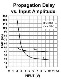
3 (1, 2) Absolute Maximum Ratings Supply Voltage...20V Input Voltage... V S + 0.3V to GND 5V Input Current (V IN > V S )...5mA Power Dissipation, T AMBIENT 25 C PDIP...960mW SOIC mW 5-Pin TO W Power Dissipation, T CASE 25 C 5-Pin TO W Derating Factors (to Ambient) PDIP...7.7mW/ C SOIC...8.3mW/ C 5-Pin TO mW/ C Storage Temperature C to +150 C Lead Temperature(10s) C Operating Ratings Operating Temperature (Chip) C Operating Temperature (Ambient) Z Version... 0 C to +70 C Y Version C to + 85 C V Version C to C Thermal Impedances (To Case) 5-Pin TO-220(θJC) C/W Electrical Characteristics (3) (T A = 25 o C, with 4.5V V S 18V unless otherwise specified.) Symbol Parameter Condition Min. Typ. Max. Units Input V IH Logic 1 Input Voltage V V IL Logic 0 Input Voltage V V IN Input Voltage Range 5 V S +.3 V I IN Input Current 0 V IN V S μa Output V OH High Output Voltage See Figure 1 V S.025 V V OL Low Output Voltage See Figure V R O Output Resistance, Output High I OUT = 10mA, V S = 18V Ω R O Output Resistance, Output Low I OUT = 10mA, V S = 18V Ω I PK Peak Output Current V S = 18V (See Figure 6) 12 A I DC Continuous Output Current 2 A I R Latch-up Protection Duty Cycle 2% Withstand Reverse Current t 300μs >1500 ma Switching Time (3) t R Rise Time Test Figure 1, C L = 15,000pF ns t F Fall Time Test Figure 1, C L = 15,000pF ns t D1 Delay Time Test Figure ns t D2 Delay Time Test Figure ns Power Supply I S Power Supply Current V IN = 3V ma V IN = 0V μa V S Operating Input Voltage 4.5 V October M B
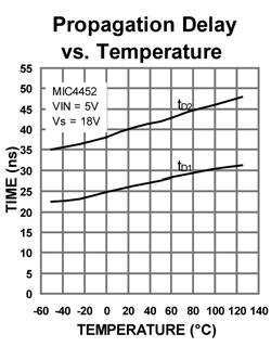
4 Electrical Characteristics (Over operating temperature range with 4.5V V S 18V unless otherwise specified.) Symbol Parameter Condition Min. Typ. Max. Units Input V IH Logic 1 Input Voltage 2.4 V V IL Logic 0 Input Voltage 0.8 V V IN Input Voltage Range 5 V S +.3 V I IN Input Current 0 V IN V S μa Output V OH High Output Voltage See Figure 1 V S.025 V V OL Low Output Voltage See Figure V R O Output Resistance, Output High I OUT = 10mA, V S = 18V 2.2 Ω R O Output Resistance, Output Low I OUT = 10mA, V S = 18V 2.2 Ω Switching Time (3) t R Rise Time Test Figure 1, C L = 15,000pF 50 ns t F Fall Time Test Figure 1, C L = 15,000pF 60 ns t D1 Delay Time Test Figure 1 65 ns t D2 Delay Time Test Figure 1 80 ns Power Supply I S Power Supply Current V IN = 3V 3 ma V IN = 0V 0.4 V S Operating Input Voltage V Notes: 1. Functional operation above the absolute maximum stress ratings is not implied. 2. Static-sensitive device. Store only in conductive containers. Handling personnel and equipment should be grounded to prevent damage from static discharge. 3. Specification for packaged product only. October M B
5 Test Circuits Figure 1. Inverting Driver Switching Time Figure 2. Noninverting Driver Switching Time Figure 3. Peak Output Current Test Circuit October M B
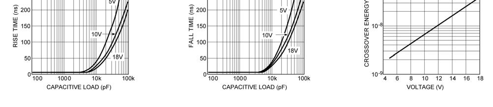
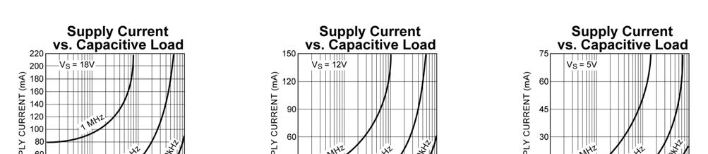
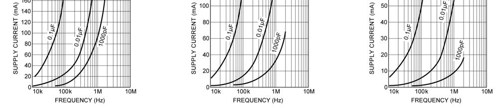
6 Typical Characteristics October M B

7 Typical Characteristics Curves (Continued) October M B
8 Applications Information Supply Bypassing Charging and discharging large capacitive loads quickly requires large currents. For example, changing a 10,000pF load to 18V in 50ns requires 3.6A. The has double bonding on the supply pins, the ground pins and output pins. This reduces parasitic lead inductance. Low inductance enables large currents to be switched rapidly. It also reduces internal ringing that can cause voltage breakdown when the driver is operated at or near the maximum rated voltage. Internal ringing can also cause output oscillation due to feedback. This feedback is added to the input signal since it is referenced to the same ground. To guarantee low supply impedance over a wide frequency range, a parallel capacitor combination is recommended for supply bypassing. Low inductance ceramic disk capacitors with short lead lengths (< 0.5 inch) should be used. A 1µF low ESR film capacitor in parallel with two 0.1µF low ESR ceramic capacitors, (such as AVX RAM GUARD ), provides adequate bypassing. Connect one ceramic capacitor directly between pins 1 and 4. Connect the second ceramic capacitor directly between pins 8 and 5. Grounding The high current capability of the demands careful PC board layout for best performance. Since the MIC4451 is an inverting driver, any ground lead impedance will appear as negative feedback which can degrade switching speed. Feedback is especially noticeable with slow-rise time inputs. The MIC4451 input structure includes 200mV of hysteresis to ensure clean transitions and freedom from oscillation, but attention to layout is still recommended. Figure 4 shows the feedback effect in detail. As the MIC4451 input begins to go positive, the output goes negative and several amperes of current flow in the ground lead. As little as 0.05Ω of PC trace resistance can produce hundreds of millivolts at the MIC4451 ground pins. If the driving logic is referenced to power ground, the effective logic input level is reduced and oscillation may result. To insure optimum performance, separate ground traces should be provided for the logic and power connections. Connecting the logic ground directly to the MIC4451 GND pins will ensure full logic drive to the input and ensure fast output switching. Both of the MIC4451 GND pins should, however, still be connected to power ground. Input Stage The input voltage level of the MIC4451 changes the quiescent supply current. The N channel MOSFET input stage transistor drives a 320µA current source load. With a logic 1 input, the maximum quiescent supply current is 400µA. Logic 0 input level signals reduce quiescent current to 80µA typical. The input is designed to provide 200mV of hysteresis. This provides clean transitions, reduces noise sensitivity, and minimizes output stage current spiking when changing states. Input voltage threshold level is approximately 1.5V, making the device TTL compatible over the full temperature and operating supply voltage ranges. Input current is less than ±10µA. The MIC4451 can be directly driven by the TL494, SG1526/1527, SG1524, TSC170, MIC38C42, and similar switch mode power supply integrated circuits. By offloading the power-driving duties to the, the power supply controller can operate at lower dissipation. This can improve performance and reliability. The input can be greater than the V S supply, however, current will flow into the input lead. The input currents can be as high as 30mA p-p (6.4mA RMS ) with the input. No damage will occur to however, and it will not latch. The input appears as a 7pF capacitance and does not change even if the input is driven from an AC source. While the device will operate and no damage will occur up to 25V below the negative rail, input current will increase up to 1mA/V due to the clamping action of the input, ESD diode, and 1kΩ resistor. Power Dissipation CMOS circuits usually permit the user to ignore power dissipation. Logic families such as 4000 and 74C have outputs which can only supply a few milliamperes of current, and even shorting outputs to ground will not force enough current to destroy the device. The on the other hand, can source or sink several amperes and drive large capacitive loads at high frequency. The package power dissipation limit can easily be exceeded. Therefore, some attention should be given to power dissipation when driving low impedance loads and/or operating at high frequency. October M B
9 +18 WIMA MKS-2 1µF Resistive Load Power Dissipation Dissipation caused by a resistive load can be calculated as: 0 V LOGIC GROUND POWER GROUND 5.0V 0.1µF 300 mv 1 MIC AMPS 6, 7 TEK CURRENT PROBE µF PC TRACE RESISTANCE = 0.05Ω 18 V 0 V 2,500 pf POLYCARBONATE P L = I 2 R O D where: I = the current drawn by the load R O = the output resistance of the driver when the output is high, at the power supply voltage used. (See data sheet) D = fraction of time the load is conducting (duty cycle) Figure 4. Switching Time Degradation Due to Negative Feedback The supply current vs. frequency and supply current vs capacitive load characteristic curves aid in determining power dissipation calculations. Table 1 lists the maximum safe operating frequency for several power supply voltages when driving a 10,000pF load. More accurate power dissipation figures can be obtained by summing the three dissipation sources. Given the power dissipation in the device, and the thermal resistance of the package, junction operating temperature for any ambient is easy to calculate. For example, the thermal resistance of the 8-pin plastic DIP package, from the data sheet, is 130 C/W. In a 25 C ambient, then, using a maximum junction temperature of 125 C, this package will dissipate 960mW. Accurate power dissipation numbers can be obtained by summing the three sources of power dissipation in the device: Load Power Dissipation (P L ) Quiescent power dissipation (P Q ) Transition power dissipation (P T ) Capacitive Load Power Dissipation Dissipation caused by a capacitive load is simply the energy placed in, or removed from, the load capacitance by the driver. The energy stored in a capacitor is described by the equation: E = 1/2 C V 2 VS 18V 15V 10V 5V Max. Frequency 220kHz 300kHz 640kHz 2MHz Table 1: MIC4451 Maximum Operating Frequency As this energy is lost in the driver each time the load is charged or discharged, for power dissipation calculations the 1/2 is removed. This equation also shows that it is good practice not to place more voltage on the capacitor than is necessary, as dissipation increases as the square of the voltage applied to the capacitor. For a driver with a capacitive load: Calculation of load power dissipation differs depending on whether the load is capacitive, resistive or inductive. P L = f C (V S ) 2 where: f = Operating Frequency C = Load Capacitance V S = Driver Supply Voltage October M B
10 Inductive Load Power Dissipation For inductive loads the situation is more complicated. For the part of the cycle in which the driver is actively forcing current into the inductor, the situation is the same as it is in the resistive case: where (A s) is a time-current factor derived from the typical characteristic curve Crossover Energy vs. Supply Voltage. Total power (P D ) then, as previously described is: P L1 = I 2 R O D However, in this instance the R O required may be either the on resistance of the driver when its output is in the high state, or its on resistance when the driver is in the low state, depending on how the inductor is connected, and this is still only half the story. For the part of the cycle when the inductor is forcing current through the driver, dissipation is best described as: P L2 = I V D (1 D) where V D is the forward drop of the clamp diode in the driver (generally around 0.7V). The two parts of the load dissipation must be summed in to produce P L : P L = P L1 + P L2 Quiescent Power Dissipation Quiescent power dissipation (P Q, as described in the input section) depends on whether the input is high or low. A low input will result in a maximum current drain (per driver) of 0.2mA; a logic high will result in a current drain of 3.0mA. Quiescent power can therefore be found from: P D = P L + P Q + P T Definitions C L = Load Capacitance in Farads. D = Duty Cycle expressed as the fraction of time the input to the driver is high. f = Operating Frequency of the driver in Hertz I H = Power supply current drawn by a driver when both inputs are high and neither output is loaded. I L = Power supply current drawn by a driver when both inputs are low and neither output is loaded. I D = Output current from a driver in Amps. P D = Total power dissipated in a driver in Watts. P L = Power dissipated in the driver due to the driver s load in Watts. P Q = Power dissipated in a quiescent driver in Watts. P T = Power dissipated in a driver when the output changes states ( shoot-through current ) in watts. R O = Output resistance of a driver in Ωs. V S = Power supply voltage to the IC in volts. P Q = V S [D I H + (1 D) I L ] where: I H = quiescent current with input high I L = quiescent current with input low D = fraction of time input is high (duty cycle) V S = power supply voltage Transition Power Dissipation Transition power is dissipated in the driver each time its output changes state, because during the transition, for a very brief interval, both the N- and P-channel MOSFETs in the output totem-pole are ON simultaneously, and a current is conducted through them from V S to ground. The transition power dissipation is approximately: P T = 2 f V S (A s) October M B
11 Package Information PIN 1 DIMENSIONS: INCH (MM) (9.65) (9.40) (3.43) (3.18) (6.48) (6.22) (7.62) (0.57) (2.54) (3.30) (0.952) (9.65) (8.13) ( ( Pin Plastic DIP (N) (0.65) MAX) PIN (3.99) (3.81) DIMENSIONS: INCHES (MM) (1.27) TYP (0.51) (0.33) (0.249) (0.102) (0.25) (0.18) (1.63) (1.14) (5.0) (4.8) SEATING PLANE (1.27) (0.40) (6.20) (5.79) 8-Pin SOIC (M) October M B
12 Package Information (Continued) 5-Pin TO-220 (T) October M B
13 MICREL, INC FORTUNE DRIVE SAN JOSE, CA USA TEL +1 (408) FAX +1 (408) WEB Micrel makes no representations or warranties with respect to the accuracy or completeness of the information furnished in this data sheet. This information is not intended as a warranty and Micrel does not assume responsibility for its use. Micrel reserves the right to change circuitry, specifications and descriptions at any time without notice. No license, whether express, implied, arising by estoppel or otherwise, to any intellectual property rights is granted by this document. Except as provided in Micrel s terms and conditions of sale for such products, Micrel assumes no liability whatsoever, and Micrel disclaims any express or implied warranty relating to the sale and/or use of Micrel products including liability or warranties relating to fitness for a particular purpose, merchantability, or infringement of any patent, copyright or other intellectual property right. Micrel Products are not designed or authorized for use as components in life support appliances, devices or systems where malfunction of a product can reasonably be expected to result in personal injury. Life support devices or systems are devices or systems that (a) are intended for surgical implant into the body or (b) support or sustain life, and whose failure to perform can be reasonably expected to result in a significant injury to the user. A Purchaser s use or sale of Micrel Products for use in life support appliances, devices or systems is a Purchaser s own risk and Purchaser agrees to fully indemnify Micrel for any damages resulting from such use or sale Micrel, Incorporated. October M B
14 Mouser Electronics Authorized Distributor Click to View Pricing, Inventory, Delivery & Lifecycle Information: Microchip: MIC4451YM MIC4452ZT MIC4452YM MIC4451YN MIC4451ZT MIC4452YN MIC4451YM-TR MIC4452YM-TR MIC4452VM-TR MIC4452VM
MIC4421/4422. Bipolar/CMOS/DMOS Process. General Description. Features. Applications. Functional Diagram. 9A-Peak Low-Side MOSFET Driver
 9A-Peak Low-Side MOSFET Driver Micrel Bipolar/CMOS/DMOS Process General Description MIC4421 and MIC4422 MOSFET drivers are rugged, efficient, and easy to use. The MIC4421 is an inverting driver, while
Features MIC4421 INVERTING. 0.3mA OUT IN MIC4422 NONINVERTING
 MIC4421/4422 9A-Peak Low-Side MOSFET Driver Bipolar/CMOS/DMOS Process General Description MIC4421 and MIC4422 MOSFET drivers are rugged, efficient, and easy to use. The MIC4421 is an inverting driver,
MIC4420/4429. General Description. Features. Applications. Functional Diagram. 6A-Peak Low-Side MOSFET Driver. Bipolar/CMOS/DMOS Process
 MIC442/4429 6A-Peak ow-side MOSFET Driver Bipolar/CMOS/DMOS Process General Description MIC442, MIC4429 and MIC429 MOSFET drivers are tough, efficient, and easy to use. The MIC4429 and MIC429 are inverting
MIC4414/4415. General Description. Features. Applications. Typical Application. 1.5A, 4.5V to 18V, Low-Side MOSFET Driver
 MIC4414/4415 1.5A, 4.5V to 18V, Low-Side MOSFET Driver General Description The MIC4414 and MIC4415 are low-side MOSFET drivers designed to switch an N-channel enhancement type MOSFET in low-side switch
MIC4478/4479/4480. General Description. Features. Applications. Typical Application. 32V Low-Side Dual MOSFET Drivers
 32V Low-Side Dual MOSFET Drivers General Description The MIC4478, MIC4479, and MIC4480 are low-side dual MOSFET drivers are designed to switch N-channel enhancement type MOSFETs from TTL-compatible control
MIC General Description. Features. Applications. Typical Application. 3A Low Voltage LDO Regulator with Dual Input Voltages
 3A Low Voltage LDO Regulator with Dual Input Voltages General Description The is a high-bandwidth, low-dropout, 3.0A voltage regulator ideal for powering core voltages of lowpower microprocessors. The
Features. *Siliconix. Load voltage limited only by MOSFET drain-to-source rating +12V MIC4416 CTL GND. Low-Side Power Switch
 MIC6/7 MIC6/7 IttyBitty Low-Side MOSFET Driver eneral Description The MIC6 and MIC7 IttyBitty low-side MOSFET drivers are designed to switch an N-channel enhancementtype MOSFET from a TTL-compatible control
Features. Applications SOT-23-5
 135MHz, Low-Power SOT-23-5 Op Amp General Description The is a high-speed, unity-gain stable operational amplifier. It provides a gain-bandwidth product of 135MHz with a very low, 2.4mA supply current,
Features INVERTING. 0.6mA OUTA INA NONINVERTING INVERTING. 0.6mA NONINVERTING
 MIC//8 MIC//8 Dual 1.-Peak Low-Side MOSFET Driver Final Information General Description The MIC//8 family are highly-reliable dual lowside MOSFET drivers fabricated on a icmos/dmos process for low power
Features. Functional Configuration IN+
 IttyBitty Rail-to-Rail Input Comparator General Description The MIC7211 and MIC7221 are micropower comparators featuring rail-to-rail input performance in Micrel s IttyBitty SOT-23-5 package. The MIC7211/21
Features INVERTING. 0.6mA NONINVERTING INVERTING. 0.6mA NONINVERTING. Ground Unused Inputs
 MIC4423/4424/4425 Dual 3A-Peak Low-Side MOSFET Driver Bipolar/CMOS/DMOS Process General Description The MIC4423/4424/4425 family are highly reliable BiCMOS/ DMOS buffer/driver/mosfet drivers. They are
PIN CONNECTIONS
 The NCP4421/4422 are high current buffer/drivers capable of driving large MOSFETs and IGBTs. They are essentially immune to any form of upset except direct overvoltage or over dissipation they cannot be
TC4467 TC4468 LOGIC-INPUT CMOS QUAD DRIVERS TC4467 TC4468 TC4469 GENERAL DESCRIPTION FEATURES APPLICATIONS ORDERING INFORMATION
 TC TC LOGIC-INPUT CMOS FEATURES High Peak Output Current....A Wide Operating Range.... to V Symmetrical Rise and Fall Times... nsec Short, Equal Delay Times... nsec Latchproof! Withstands ma Inductive
MIC4223/MIC4224/MIC4225
 Dual 4A, 4.5V to 18V, 15ns Switch Time, Low-Side MOSFET Drivers with Enable General Description The are a family of a dual 4A, High-Speed, Low-side MOSFET drivers with logic-level driver enables. The devices
MIC5388/9. Features. General Description. Applications. Typical Application. Dual 200mA Peak LDO in Wafer Level Chip Scale Package
 Dual 2mA Peak LDO in Wafer Level Chip Scale Package General Description The is an advanced dual LDO ideal for powering general purpose portable devices. The provides two independently-controlled, highperformance,
Features. Applications
 Teeny Ultra-Low-Power Op Amp General Description The is a rail-to-rail output, input common-mode to ground, operational amplifier in Teeny SC70 packaging. The provides a 400kHz gain-bandwidth product while
MIC833. General Description. Features. Applications. Typical Application. Comparator and Reference with Adjustable Hystersis
 Comparator and Reference with Adjustable Hystersis General Description The is a micropower precision dual voltage comparator with an on-chip reference and latch. High- and low-voltage thresholds are adjusted
MIC5271. Applications. Low. output current). Zero-current off mode. and reduce power. GaAsFET bias Portable cameras. le enable pin, allowing the user
. Zero-current off mode. and reduce power. GaAsFET bias Portable cameras. le enable pin, allowing the user") µcap Negative Low-Dropout Regulator General Description The is a µcap 100mA negativee regulator in a SOT-23-this regulator provides a very accurate supply voltage for applications that require a negative
µcap Negative Low-Dropout Regulator General Description The is a µcap 100mA negativee regulator in a SOT-23-this regulator provides a very accurate supply voltage for applications that require a negative
MIC5365/6. General Description. Features. Applications. Typical Application. High-Performance Single 150mA LDO
 High-Performance Single 150mA LDO General Description The is an advanced general purpose linear regulator offering high power supply rejection (PSRR) in an ultra-small 1mm 1mm package. The MIC5366 includes
MIC5524. Features. General Description. Applications. Typical Application. High-Performance 500mA LDO in Thin DFN Package
 High-Performance 500mA LDO in Thin DFN Package General Description The is a low-power, µcap, low dropout regulator designed for optimal performance in a very-small footprint. It is capable of sourcing
Features. Applications
 Teeny Ultra-Low Power Op Amp General Description The is a rail-to-rail output, operational amplifier in Teeny SC70 packaging. The provides 4MHz gain-bandwidth product while consuming an incredibly low
Features MIC2193BM. Si9803 ( 2) 6.3V ( 2) VDD OUTP COMP OUTN. Si9804 ( 2) Adjustable Output Synchronous Buck Converter
 6.3V ( 2) VDD OUTP COMP OUTN. Si9804 ( 2) Adjustable Output Synchronous Buck Converter") MIC2193 4kHz SO-8 Synchronous Buck Control IC General Description s MIC2193 is a high efficiency, PWM synchronous buck control IC housed in the SO-8 package. Its 2.9V to 14V input voltage range allows
MIC2193 4kHz SO-8 Synchronous Buck Control IC General Description s MIC2193 is a high efficiency, PWM synchronous buck control IC housed in the SO-8 package. Its 2.9V to 14V input voltage range allows
Features. Slope Comp Reference & Isolation
 MIC388/389 Push-Pull PWM Controller General Description The MIC388 and MIC389 are a family of complementary output push-pull PWM control ICs that feature high speed and low power consumption. The MIC388/9
MIC94161/2/3/4/5. Features. General Description. Applications. Typical Application. 3A High-Side Load Switch with Reverse Blocking
 3A High-Side Load Switch with Reverse Blocking General Description The is a family of high-side load switches designed to operate from 1.7V to 5.5V input voltage. The load switch pass element is an internal
Features. Applications
 105MHz Low-Power SOT23-5 Op Amp General Description The is a high-speed operational amplifier which is unity gain stable regardless of resistive and capacitive load. It provides a gain-bandwidth product
Features. Applications
 High-Current Low-Dropout Regulators General Description The is a high current, high accuracy, lowdropout voltage regulators. Using Micrel's proprietary Super βeta PNP process with a PNP pass element, these
Features. Applications
 High PSRR Low Noise 300mA µcap Ultra-Low Dropout LDO Regulator General Description The is a high-performance, 300mA LDO regulator, offering extremely high PSRR and very low noise while consuming low ground
Features. Applications
 PCIe Fanout Buffer 267MHz, 8 HCSL Outputs with 2 Input MUX PrecisionEdge General Description The is a high-speed, fully differential 1:8 clock fanout buffer optimized to provide eight identical output
Adaptive Power MOSFET Driver 1
 Adaptive Power MOSFET Driver 1 FEATURES dv/dt and di/dt Control Undervoltage Protection Short-Circuit Protection t rr Shoot-Through Current Limiting Low Quiescent Current CMOS Compatible Inputs Compatible
MIC38C42A/43A/44A/45A
 MIC38C42A/43A/44A/45A BiCMOS Current-Mode PWM Controllers General Description The MIC38C4xA are fixed frequency, high performance, current-mode PWM controllers. Micrel s BiCMOS devices are pin compatible
Features. +12V to +36V MIC nf. High-Side Driver with Overcurrent Trip and Retry
 MIC0 MIC0 High-Speed High-Side MOSFET Driver General Description The MIC0 high-side MOSFET driver is designed to operate at frequencies up to 00kHz (khz PWM for % to 00% duty cycle) and is an ideal choice
MIC5317. Features. General Description. Applications. Typical Application. High-Performance Single 150mA LDO
 High-Performance Single 150mA LDO General Description The is a high performance 150mA low dropout regulator offering high power supply rejection (PSRR) in an ultra-small 1mm 1mm package for stringent space
SY84782U. General Description. Features. Typical Application. Low Power 2.5V 1.25Gbps FP/DFB Laser Diode Driver
 Low Power 2.5V 1.25Gbps FP/DFB Laser Diode Driver General Description Features The is a single 2.5V supply, ultra-low power, small form factor laser diode driver for telecom/datacom applications. Intended
MIC4812. Features. General Description. Applications. Typical Application
 High Current 6 Channel Linear WLED Driver with DAM and Ultra Fast PWM Control General Description The is a high efficiency linear White LED (WLED) driver designed to drive up to six high current WLEDs
MIC69151/153. General Description. Features. Applications. Typical Application. Single Supply V IN, Low V IN, Low V OUT, 1.5A LDO
 Single Supply V IN, Low V IN, Low V OUT, 1.5A LDO General Description The is the 1.5A output current member of the MIC69xxx family of high current, low voltage regulators, which support currents of 1A,
MIC5501/2/3/4. General Description. Features. Applications. Typical Application. Single 300mA LDO in 1.0mm 1.0mm DFN Package
 Single 300mA LDO in 1.0mm 1.0mm DFN Package General Description The is an advanced general-purpose LDO ideal for powering general-purpose portable devices. The family of products provides a highperformance
MIC5396/7/8/9. General Description. Features. Applications. Typical Application. Low-Power Dual 300mA LDO in 1.2mm x 1.
 Low-Power Dual 300mA LDO in 1.2mm x 1.6mm Extra Thin DFN General Description The is an advanced dual LDO ideal for powering general purpose portable devices. The provides two high-performance, independent
TC4421/TC A High-Speed MOSFET Drivers. General Description. Features. Applications. Package Types (1)
") 9A High-Speed MOSFET Drivers Features High Peak Output Current: 9A Wide Input Supply Voltage Operating Range: - 4.5V to 18V High Continuous Output Current: 2A Max Fast Rise and Fall Times: - 3 ns with
9A High-Speed MOSFET Drivers Features High Peak Output Current: 9A Wide Input Supply Voltage Operating Range: - 4.5V to 18V High Continuous Output Current: 2A Max Fast Rise and Fall Times: - 3 ns with
Features. Micrel Inc Fortune Drive San Jose, CA USA tel +1 (408) fax + 1 (408)
 fax + 1 (408)") Low Power, 1.62V to 3.63V, 10MHz to 40MHz, 1:2 Oscillator Fanout Buffer Revision 2.0 General Description The is an advanced oscillator fanout buffer design for high performance, low-power, small form-factor
Low Power, 1.62V to 3.63V, 10MHz to 40MHz, 1:2 Oscillator Fanout Buffer Revision 2.0 General Description The is an advanced oscillator fanout buffer design for high performance, low-power, small form-factor
SM ClockWorks 10-Gigabit Ethernet, MHz, Ultra-Low Jitter LVPECL Clock Frequency Synthesizer. General Description.
 ClockWorks 10-Gigabit Ethernet, 156.25MHz, Ultra-Low Jitter LVPECL Clock Frequency Synthesizer General Description The is a 10-Gigabit Ethernet, 156.25MHz LVPECL clock frequency synthesizer and a member
Features. Applications
 Ultra-Precision, 8:1 MUX with Internal Termination and 1:2 LVPECL Fanout Buffer Precision Edge General Description The is a low-jitter, low-skew, high-speed 8:1 multiplexer with a 1:2 differential fanout
Features. Applications
 Comparator with 1.25% Reference and Adjustable Hysteresis General Description The MIC841 and MIC842 are micropower, precision voltage comparators with an on-chip voltage reference. Both devices are intended
Features. MIC5318-x.xYMT EN BYP GND. Portable Application
 High Performance 3mA µcap ULDO General Description The is a high performance, single output ultra low drop-out (ULDO ) regulator, offering low total output noise in an ultra-small Thin MLF package. The
Features. Applications SOT-23-5 (M5)
") 1.8V to 11V, 15µA, 25kHz GBW, Rail-to-Rail Input and Output Operational Amplifier General Description The is a low-power operational amplifier with railto-rail inputs and outputs. The device operates from
1.8V to 11V, 15µA, 25kHz GBW, Rail-to-Rail Input and Output Operational Amplifier General Description The is a low-power operational amplifier with railto-rail inputs and outputs. The device operates from
Features. Applications
 MIC67 IttyBitty Comparator General Description The MIC67 is a precision voltage comparator with an offset voltage specification of maximum. The MIC67 is designed to operate from a single V to 6V power
Features. Applications
 Dual 500mA µcap Low Dropout, Micropower Linear Regulator General Description The is an advanced dual, micropower, low dropout linear regulator. The provides low quiescent current operation, using only
Features. Applications. Markets
 2GHz, Low-Power, 1:6 LVPECL Fanout Buffer with 2:1 Input MUX and Internal Termination General Description The is a 2.5V/3.3V precision, high-speed, 1:6 fanout capable of handling clocks up to 2.0GHz. A
MIC5018. General Description. Features. Applications. Typical Applications. IttyBitty High-Side MOSFET Driver
 IttyBitty High-Side MOSFET Driver General Description The IttyBitty high-side MOSFET driver is designed to switch an N-channel enhancement-type MOSFET from a TTL compatible control signal in high- or low-side
Features. Applications. Markets
 3.2Gbps Precision, LVPECL Buffer with Internal Termination and Fail Safe Input General Description The is a 2.5/3.3V, high-speed, fully differential LVPECL buffer optimized to provide only 108fs RMS phase
Features. 5V Reference UVLO. Oscillator S R GND*(AGND) 5 (9) ISNS 3 (5)
 5 (9) ISNS 3 (5)") MIC38HC42/3/4/5 BiCMOS 1A Current-Mode PWM Controllers General Description The MIC38HC4x family are fixed frequency current-mode PWM controllers with 1A drive current capability. Micrel s BiCMOS devices
MIC38HC42/3/4/5 BiCMOS 1A Current-Mode PWM Controllers General Description The MIC38HC4x family are fixed frequency current-mode PWM controllers with 1A drive current capability. Micrel s BiCMOS devices
Features MIC1555 VS MIC1557 VS OUT 5
 MIC555/557 MIC555/557 IttyBitty RC Timer / Oscillator General Description The MIC555 IttyBitty CMOS RC timer/oscillator and MIC557 IttyBitty CMOS RC oscillator are designed to provide rail-to-rail pulses
Features. 5V Reference UVLO. Oscillator S R
 MIC38C42/3/4/5 BiCMOS Current-Mode PWM Controllers General Description The MIC38C4x are fixed frequency, high performance, current-mode PWM controllers. Micrel s BiCMOS devices are pin compatible with
Features. Applications. RF Power Supply Circuit
 High Performance, Low Noise Dual 500mA ULDO General Description The is a tiny Dual Ultra Low Dropout (ULDO ) linear regulator ideally suited for portable electronics due to its low output noise. The provides
Features MIC5022 C TH. Sense H+ C TL. Sense L. DC Motor Control Application
 MIC0 MIC0 Half-Bridge MOSFET Driver Not Recommended for New Designs General Description The MIC0 half-bridge MOSFET driver is designed to operate at frequencies up to 00kHz (khz PWM for % to 00% duty cycle)
Features. Applications
 Comparator with 1.25% Reference and Adjustable Hysteresis General Description The MIC841 and MIC842 are micro-power, precisionvoltage comparators with an on-chip voltage reference. Both devices are intended
NOT RECOMMENDED FOR NEW DESIGNS. Features. Applications. Markets
 NOT RECOMMENDED FOR NEW DESIGNS Low Voltage 1.2V/1.8V/2.5V CML 2x2 Crosspoint Switch 6.4Gbps with Equalization General Description The is a fully-differential, low-voltage 1.2V/1.8V/2.5V CML 2x2 crosspoint
Features. Applications
 3.0A, Low-Voltage µcap LDO Regulator General Description The Micrel is a 3.0A low-dropout linear voltage regulator that provides a low voltage, high current output with a minimum number of external components.
Features. Applications
 PCIe Octal, Ultra-Low Jitter, HCSL Frequency Synthesizer General Description The PL607081 and PL607082 are members of the PCI Express family of devices from Micrel and provide extremely low-noise spread-spectrum
Features. Applications
 267MHz 1:2 3.3V HCSL/LVDS Fanout Buffer PrecisionEdge General Description The is a high-speed, fully differential 1:2 clock fanout buffer with a 2:1 input MUX optimized to provide two identical output
MIC803. Features. General Description. Applications. Typical Application. 3-Pin Microprocessor Supervisor Circuit with Open-Drain Reset Output
 3-Pin Microprocessor Supervisor Circuit with Open-Drain Reset Output General Description The is a single-voltage supervisor with open-drain reset output that provides accurate power supply monitoring and
Adaptive Power MOSFET Driver 1
 End of Life. Last Available Purchase Date is 3-Dec-204 Si990 Adaptive Power MOSFET Driver FEATURES dv/dt and di/dt Control Undervoltage Protection Short-Circuit Protection t rr Shoot-Through Current Limiting
MIC5332. Features. General Description. Applications. Typical Application. Micro-Power, High-Performance Dual 300mA ULDO
 Micro-Power, High-Performance Dual 300mA ULDO General Description The is a tiny, dual, low quiescent current LDO ideal for applications that are power sensitive. The integrates two high-performance 300mA
SM Features. General Description. Applications. Block Diagram. ClockWorks GbE (125MHz) Ultra-Low Jitter, LVPECL Frequency Synthesizer
 Ultra-Low Jitter, LVPECL Frequency Synthesizer") ClockWorks GbE (125MHz) Ultra-Low Jitter, LVPECL Frequency Synthesizer General Description The is a member of the ClockWorks family of devices from Micrel and provides an extremely low-noise timing solution
ClockWorks GbE (125MHz) Ultra-Low Jitter, LVPECL Frequency Synthesizer General Description The is a member of the ClockWorks family of devices from Micrel and provides an extremely low-noise timing solution
SY88992L. Features. General Description. Applications. Markets. Typical Application. 3.3V, 4.25Gbps VCSEL Driver
 3.3V, 4.25Gbps VCSEL Driver General Description The is a single supply 3.3V, low power consumption, small-form factor VCSEL driver ideal for use in datacom applications; Ethernet, GbE (Gigabit Ethernet),
Features. Applications
 Ultra-Precision 1:8 LVDS Fanout Buffer with Three 1/ 2/ 4 Clock Divider Output Banks Revision 6.0 General Description The is a 2.5V precision, high-speed, integrated clock divider and LVDS fanout buffer
Features V IN LM2574 OUT PWR GND SIG GND ON/ 11DQ05 OFF. Figure 1. Fixed Output Regulator Circuit
 52kHz Simple.5A Buck Regulator General Description The family is a series of easy to use fixed and adjustable switching voltage regulators. The contains all of the active circuitry necessary to construct
MIC5370/1. Features. General Description. Applications. Typical Application. High-Performance Dual 150mA LDO 1.6mm x 1.
 High-Performance Dual 15mA LDO 1.6mm x 1.6mm General Description The is an advanced dual LDO ideal for powering general purpose portable devices. The provides two independently-controlled, highperformance
Features. Truth Table (1)
") 3.3V/5V, 4GHz PECL/ECL 2 Clock Generator Precision Edge General Description The is an integrated 2 divider with differential clock inputs. It is functionally equivalent to the SY100EP32V but in an ultra-small
3.3V/5V, 4GHz PECL/ECL 2 Clock Generator Precision Edge General Description The is an integrated 2 divider with differential clock inputs. It is functionally equivalent to the SY100EP32V but in an ultra-small
Features. 7V 40V Unregulated DC Input 1 +V IN + C IN
 LM76 khz Simple 3A Buck Regulator General Description The LM76 series of monolithic integrated circuits provide all the active functions for a step-down (buck) switching regulator. Fixed versions are available
TC4427 TC A DUAL HIGH-SPEED POWER MOSFET DRIVERS 1.5A DUAL HIGH-SPEED POWER MOSFET DRIVERS TC4426 TC4426 GENERAL DESCRIPTION FEATURES
 FEATURES High Peak Output Current....A Wide Operating Range....V to V High Capacitive Load Drive Capability... pf in nsec Short Delay Time... < nsec Typ. Consistent Delay Times With Changes in Supply Voltage
Features. Applications GND. Micrel Inc Fortune Drive San Jose, CA USA tel +1 (408) fax + 1 (408)
 fax + 1 (408)") 3-Pin Microprocessor Supervisor Circuit with Open-Drain Reset Output General Description The is a single-voltage supervisor with open-drain reset output that provides accurate power supply monitoring and
3-Pin Microprocessor Supervisor Circuit with Open-Drain Reset Output General Description The is a single-voltage supervisor with open-drain reset output that provides accurate power supply monitoring and
Features. Applications. Micrel Inc Fortune Drive San Jose, CA USA tel +1 (408) fax + 1 (408)
 fax + 1 (408)") 3.3V 10.7Gbps CML Limiting Post Amplifier with TTL SD and /SD General Description The high-speed, limiting post amplifier is designed for use in fiber-optic receivers. The device connects to typical transimpedance
3.3V 10.7Gbps CML Limiting Post Amplifier with TTL SD and /SD General Description The high-speed, limiting post amplifier is designed for use in fiber-optic receivers. The device connects to typical transimpedance
SY89297U. General Description. Features. Applications. Markets. 2.5/3.3V, 3.2Gbps Precision CML Dual-Channel Programmable Delay
 2.5/3.3V, 3.2Gbps Precision CML Dual-Channel Programmable Delay General Description The is a DC-3.2Gbps programmable, twochannel delay line. Each channel has a delay range from 2ns to 7ns (5ns delta delay)
Features. Applications. Markets
 Low Voltage 1.2V/1.8V CML Differential Line Driver/Receiver 3.2Gbps, 3.2GHz General Description The is a fully-differential, low-voltage 1.2V/1.8V CML Line Driver/Receiver. The can process clock signals
Features. Applications
 IttyBitty RC Timer/Oscillator General Description The MIC1555 IttyBitty CMOS RC timer/oscillator and MIC1557 IttyBitty CMOS RC oscillator are designed to provide rail-to-rail pulses for precise time delay
MIC37150/51/52/53. General Description. Features. Applications. Typical Application. 1.5A, Low Voltage µcap LDO Regulator
 1.5A, Low Voltage µcap LDO Regulator General Description The Micrel is a 1.5A low-dropout linear voltage regulator that provides a low voltage, high current output with a minimum of external components.
Features V OUT C BYP. Ultra-Low-Noise Regulator Application
 MIC525 MIC525 5mA Low-Noise LDO Regulator Final Information General Description The MIC525 is an efficient linear voltage regulator with ultralow-noise output, very low dropout voltage (typically 7mV at
Features. Ordering Information. Part Number Standard Marking Pb-Free Marking
 MIC9 MIC9 8MHz Low-Power SC-7 Op Amp General Description The MIC9 is a high-speed operational amplifier with a gain-bandwidth product of 8MHz. The part is unity gain stable. It has a very low µa supply
Features MIC2194BM VIN EN/ UVLO CS OUTP VDD FB. 2k COMP GND. Adjustable Output Buck Converter MIC2194BM UVLO
 MIC2194 400kHz SO-8 Buck Control IC General Description s MIC2194 is a high efficiency PWM buck control IC housed in the SO-8 package. Its 2.9V to 14V input voltage range allows it to efficiently step
Features. Applications
 IttyBitty Integrated High-Side Switch General Description The is an integrated high-side power switch that consists of a TTL compatible input and protected P- channel MOSFET. The can be used instead of
Features. Applications
 Ultra-Precision CML Data and Clock Synchronizer with Internal Input and Output Termination Precision Edge General Description The is an ultra-fast, precision, low jitter datato-clock resynchronizer with
SY88982L. Features. General Description. Applications. Markets. Typical Application
 3.3V, 2.7Gbps High-Current, Low-Power Laser Driver for FP/DFB Lasers General Description The is a single 3.3V supply, low power consumption, small form factor driver for telecom/datacom applications using
MIC5248. Features. General Description. Applications. Typical Application. 150mA µcap CMOS LDO Regulator w/power Good VIN VOUT C OUT GND
 150mA µcap CMOS LDO Regulator w/power Good General Description The is an efficient, general purpose 1.2V CMOS voltage regulator with a power good output function. The offers better than 3%initial accuracy,
Features. Applications
 MIC532 15mA ULDO in Ultra-Small 1.2mm x 1.6mm Thin MLF General Description The MIC532 is an ultra-small, ultra-low dropout CMOS regulator, ULDO that is ideal for today s most demanding portable applications
Features. Applications V IN ENABLE SHUTDOWN. C IN = 1.0µF
 300mA High PSRR, Low Noise µcap CMOS LDO General Description The is an efficient CMOS voltage regulator optimized for low-noise applications. It offers 1.5% initial accuracy, low dropout voltage (300mV
MIC37110/MIC37112 MIC37120/MIC37122
 High-Performance, Low-Noise, 1A LDOs General Description The and are high-performance, low-noise, low dropout regulators. Each of these LDOs is capable of sourcing 1A output current, offers high power
MIC5225. General Description. Features. Applications. Typical Application. Ultra-Low Quiescent Current 150mA µcap Low Dropout Regulator
 Ultra-Low Quiescent Current 15mA µcap Low Dropout Regulator General Description The is a 15mA highly accurate, low dropout regulator with high input voltage and ultra-low ground current. This combination
Features. Applications. Battery-Powered Regulator Application
 180mA Low-Noise LDO Regulator General Description The is an efficient linear voltage regulator with ultra-low-noise output, very low dropout voltage (typically 17 at light loads and 165 at 150mA), and
Features. RAMP Feed Forward Ramp/ Volt Sec Clamp Reference & Isolation. Voltage-Mode Half-Bridge Converter CIrcuit
 MIC3838/3839 Flexible Push-Pull PWM Controller General Description The MIC3838 and MIC3839 are a family of complementary output push-pull PWM control ICs that feature high speed and low power consumption.
Features. Applications. Micrel Inc Fortune Drive San Jose, CA USA tel +1 (408) fax + 1 (408)
 fax + 1 (408)") Revision 1.1 General Description The series is a low-power, small form-factor, high-performance OTP-based device and a member of Micrel s JitterBlocker, factory programmable jitter attenuators. The JitterBlocker
Revision 1.1 General Description The series is a low-power, small form-factor, high-performance OTP-based device and a member of Micrel s JitterBlocker, factory programmable jitter attenuators. The JitterBlocker
MIC5206. General Description. Features. Applications. Typical Application. 150mA Low-Noise LDO Regulator
 MIC526 5mA Low-Noise LDO Regulator General Description The MIC526 is an efficient linear voltage regulator with very low dropout voltage (typically 7 at light loads and 65 at 5mA), and very low ground
Features. Applications. Adjustable Regulator Application. (*See Minimum Load Current Section)
") 3A, Low Voltage µcap LDO Regulator General Description The is a 3A low-dropout linear voltage regulator that provides a low voltage, high current output with a minimum of external components. It offers
3A, Low Voltage µcap LDO Regulator General Description The is a 3A low-dropout linear voltage regulator that provides a low voltage, high current output with a minimum of external components. It offers
MAX15070A/MAX15070B 7A Sink, 3A Source, 12ns, SOT23 MOSFET Drivers
 General Description The /MAX15070B are high-speed MOSFET drivers capable of sinking 7A and sourcing 3A peak currents. The ICs, which are an enhancement over MAX5048 devices, have inverting and noninverting
IXDN414PI / N414CI / N414YI / N414SI IXDI414PI / I414CI / I414YI / I414SI 14 Ampere Low-Side Ultrafast MOSFET and IGBTDrivers. General Description
 Ampere Low-Side Ultrafast MOSFET and IGBTDrivers Features Built using the advantages and compatibility of CMOS and IXYS HDMOS TM processes Latch-Up Protected Over Entire Operating Range High Peak Output
Low Cost, General Purpose High Speed JFET Amplifier AD825
 a FEATURES High Speed 41 MHz, 3 db Bandwidth 125 V/ s Slew Rate 8 ns Settling Time Input Bias Current of 2 pa and Noise Current of 1 fa/ Hz Input Voltage Noise of 12 nv/ Hz Fully Specified Power Supplies:
Features. Ordering Information. Part Identification
 MIC9 MHz Low-Power SC-7 Op Amp General Description The MIC9 is a high-speed operational amplifier with a gain-bandwidth product of MHz. The part is unity gain stable. It has a very low.ma supply current,
Package Type. IXDD604D2TR 8-Pin DFN Tape & Reel Pin Power SOIC with Exposed Metal Back Tube 100
 -Ampere Dual Low-Side Ultrafast MOSFET Drivers Features A Peak Source/Sink Drive Current Wide Operating oltage Range:.5 to 35 - C to +5 C Extended Operating Temperature Range Logic Input Withstands Negative
Features. Applications
 High Input Voltage Low IQ µcap LDO Regulator General Description The is a 100mA highly accurate, low dropout regulator with high input voltage and ultra-low ground current. This combination of high voltage
Single Supply, Low Power, Triple Video Amplifier AD8013
 a FEATURES Three Video Amplifiers in One Package Drives Large Capacitive Load Excellent Video Specifications (R L = 5 ) Gain Flatness. db to MHz.% Differential Gain Error. Differential Phase Error Low
MIC General Description. Features. Applications. Typical Application. 1.5A Low Voltage LDO Regulator w/dual Input Voltages
 MIC4915 1.5A Low oltage LDO Regulator w/dual Input oltages General Description The MIC4915 is a high-bandwidth, low-dropout, 1.5A voltage regulator ideal for powering core voltages of lowpower microprocessors.