Atomic Resolution Imaging with a sub-50 pm Electron Probe
|
|
|
- Myles Sherman
- 5 years ago
- Views:
Transcription
1 Atomic Resolution Imaging with a sub-50 pm Electron Probe Rolf Erni, Marta D. Rossell, Christian Kisielowski, Ulrich Dahmen National Center for Electron Microscopy, Lawrence Berkeley National Laboratory Berkeley, CA 9470 USA. Using a highly coherent focused electron probe in a 5 th order aberration-corrected transmission electron microscope, we report on resolving a crystal spacing less than 50 pm. Based on the geometrical source size and residual coherent and incoherent axial lens aberrations, an electron probe is calculated, which is theoretically capable of resolving an ideal 47 pm spacing with 9% contrast. Our experimental data show the 47 pm spacing of a Ge 114 crystal imaged with 11-18% contrast at a 60-95% confidence level, providing the first direct evidence for sub 50-pm resolution in ADF STEM imaging. PACS numbers: p, Gy, Ma, s Recent advances in aberration-correcting electron optics have made sub-ångstrom imaging in transmission electron microscopy almost routine in both the broad beam and the scanning probe modes [1-4]. The desire to further improve the spatial resolution in electron microscopy is driven in large part by the need for increased sensitivity, image contrast [5] and atomic-resolution tomography [6]. In this Letter, we report on utilizing a new generation aberration-corrected microscope to form a highly coherent sub-50 pm electron probe at 300 kv and demonstrate that this probe is capable of resolving the 47 pm dumbbell spacing in a Ge 114 crystal. In scanning transmission electron microscopy (STEM), the size of the electron probe that is focused onto the specimen ultimately limits the spatial resolution. Apart from mechanical and electrical stability, the size of the probe is determined by the illumination half-angle α, residual coherent axial aberrations, and incoherent broadening due to partial temporal and partial spatial coherence given by the finite energy length and the finite size of the demagnified electron source, respectively. 1
2 Previous efforts to improve the spatial resolution in STEM have mainly focused on minimizing phase shifts caused by lens aberrations in order to increase the illumination angle and hence, to reduce the impact of the diffraction limit on the lateral resolution. Strategies to optimize the electron probe by improving the electron-optical set-up have largely neglected the finite size of the electron source, thus implying infinite source brightness and demagnification. Here, we consider the effect of the finite size of the electron source using the geometrical source size, which corresponds to the size of the demagnified electron source that is imaged onto the specimen. For a given electron energy E 0, the coherent point source contribution to the electron probe in the aperture plane can be expressed as ψ ( ω) πi = exp χ( ω) λ ωω α 1 exp + δ α 1. (1) The complex coordinate in the aperture plane is ω and ω is its complex conjugate, λ=λ(e 0 ) is the electron wavelength and χ(ω) is the aberration function [7]. The first term expresses aberration phase shifts and the second term is the aperture function. The parameter δ α can be chosen as a small fraction of α in order to minimize artifacts that can arise in the numerical treatment of ψ ( ω) when a sharp edge function is considered [8]. Knowing the brightness β of the electron source, the current of the electron probe I P and the angle α, the geometrical source size d geo (FWHM) can be estimated by geo d = 4I /( π α β ) [9]. To incorporate the effect of partial spatial coherence we P assume a Gaussian source distribution function S 1 ww ( w) exp πσ σ S = S. () The standard deviation σ S is related to d geo by σ S = d geo / 8ln, and w denotes the complex coordinate in the specimen plane. The probe intensity is then expressed by ψ ( w) S( w), where ψ ( w) is the Fourier transform of ( ω) convolution. ψ and denotes Partial temporal coherence leads to an additional incoherent broadening of the electron probe. This effect is determined by the energy spread of the source and the constant of
3 chromatic aberration C C. Due to the variation δe of electron energies around E 0, the chromatic aberration causes a variation of the defocus C 1 given by δc1=c C δe/e 0 which directly affects the aberration function χ(ω) in Eq. (1). Hence, the probe wave field ψ ( w) becomes a function of energy E. The intensity of the electron probe is then given by I with dt ( ) ( E) ( w) = ( w, E) S( w) dt de ψ de, (4) de ( E) 1 ( E E ) 0 = exp πσ σ T T. (5) Eq. (5) describes a Gaussian distribution of electron energies E around E 0 with σ T = E / 8ln and E is the FWHM of the energy spread [7]. Calculating a 300 kev aberration-free (χ = 0) electron probe according to Eq. (4) for α=8.9 mrad and d geo =50 pm, considering partial temporal coherence due to an energy length C C E of 1.68 mm ev, yields a probe intensity profile of 53 pm FWHM. Reducing the energy length by a factor of two results in a probe of 47 pm, whereas a reduction of d geo by a factor of two shrinks the probe to less than 38 pm. Thus the effect of d geo on the probe size highlights the importance of source brightness and partial spatial coherence [10] in STEM imaging. In this work, we present evidence for a sub-50 pm electron probe formed in a new generation aberration-corrected transmission electron microscope that has been developed as part of the TEAM (Transmission Electron Aberration-corrected Microscopy) project [11]. The TEAM 0.5 microscope is equipped with a novel Schottkytype high-brightness field-emission electron source and an improved hexapole-type illumination aberration corrector [1]. The brightness β of the electron source was ~ A/(cm srad) at 300 kv. We employed an electron probe of I P =46 pa at an illumination half-angle α of 8.9 mrad, implying a geometrical source size of ~5 pm. The probe corrector enables the correction of aberrations up to 5th order spherical aberration C 5. The following aberration coefficients were measured (notation see, e.g., [7]); A =4 nm, B =8 nm, C 3 =-149 nm, A 3 =97 nm, S 3 =90 nm, A 4 =10. µm, D 4 =7. µm, B 4 =5.5 µm, C 5 =509 µm, A 5 =1 µm, S 5 =7 µm, and R 5 =4 µm [11]. Defocus C 1 and two- 3
4 fold astigmatism A 1 were manually optimized. The illumination angle was chosen in order to balance the impact of the diffraction limit against residual coherent aberrations and, considering the finite energy length of 1.68 mm ev, to minimize probe tails that arise if a too large angle is chosen. Figure 1(a) presents an annular dark-field (ADF) STEM micrograph of a Ge foil in 114 zone axis orientation that was recorded with an electron probe having the characteristics described above. The 114 projection of Ge consists of a periodic array of pairs of atom columns that are separated by 47 pm. Due to glide-mirror symmetry, the two columns of atoms forming the dumbbell are shifted with respect to each other by 0.47 nm in the direction of projection. The crystal planes corresponding to the 47 pm distance are of the type {884}. Atoms along each column are separated by 1. nm. The micrograph was recorded using a magnification corresponding to a Nyquist frequency of 50./nm (9.95 pm/pixel), a dwell time of 7 µs and an annular detection range of ~45-90 mrad (semi-angle). The signal amplifier was adjusted to utilize the full dynamic range of the detector without clipping the signal. The Ge specimen was cut in a 114 orientation from a 001 -Ge wafer and mechanically polished, followed by Ar ion milling. The estimated sample thickness is ~10 nm. Fig. 1(b) shows the micrograph after high-frequency noise-reduction using a low-pass filter set at 40 pm with the edge of the Fourier mask smoothed from 3 and 40 pm. Single-pixel line profiles along the atom row of the Region of Interest (RoI) 1 in Fig. 1(a) and of the equivalent row from the filtered micrograph in Fig. 1(b) are shown in Fig. (a). The power spectrum and the line profiles in Fig. confirm the presence of the 884 image frequency as well as other sub-50 pm reflections. The 880 reflection (50 pm) in the direction perpendicular to [ 44] is weakly present but falls into an area of the power spectrum that is affected by residual scan noise. From Fig. 1 and the line profile in Fig. (a), it is clear that the 47 pm dumbbell splitting is observed locally but not everywhere because the micrograph is affected by noise. In the presence of noise, resolution depends on the significance with which a signal can be detected above the noise level [13]. In order to quantitatively assess the noise level as well as the statistical relevance of the sub-50 pm information we performed local 4
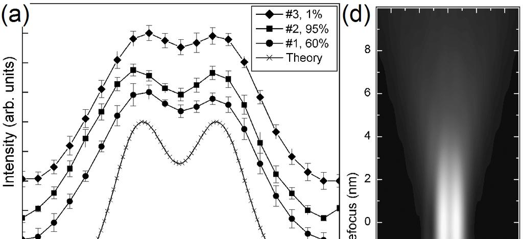
5 statistical analyses for the RoIs in Fig. 1(a). For each of the three RoIs we derived the average dumbbell structure and the corresponding noise. The line profiles in Fig. 3(a) across the averaged structures reveal dips of 11%, 18% and 8% contrast for RoI 1, and 3, respectively. The averaged structure of RoI 1 is shown in Fig. 3(c). The error bars in Fig. 3(a) are the standard deviations obtained by comparing the individual dumbbells with the averaged structures [14]. From the standard deviation for each pixel, the dumbbell dip can be characterized with a confidence level. The 11% dumbbell contrast in RoI 1 is measured with a confidence level of 60%, while the 18% contrast in RoI has a confidence level of 95%. These confidence levels reflect the statistical significance of observing the 47 pm splitting in individual image unit cells. By comparison, RoI 3 shows only 8% contrast with a confidence level of merely 1%, indicating that in this area, the dumbbell spacing has not been resolved. However, the result of RoI 1 and provides clear evidence supporting the presence of a sub-50 pm electron probe and the 47 pm instrument resolution. Electron-probe calculations according to Eq. (4) for an energy length of 1.68 mm ev yield a theoretical electron probe of 41 pm FWHM, assuming that the overall instrument stability preserves the brightness from source to specimen. Instabilities of high temporal frequency would lead to an effective blurring of d geo [15], whereas instabilities of lower frequencies would cause apparent scan noise. For an object that consists of two deltafunctions separated by 47 pm the theoretical contrast can be found by convoluting the idealized object with the calculated electron probe, see Fig. 3(b). The line profile of the calculated dumbbell in Fig. 3(a) reveals a dip of 9%, representing the instrument resolution achievable for the theoretical electron probe and an idealized 47 pm spacing. Comparing theoretical instrument resolution with an experimental micrograph raises the question of the extent to which the specimen limits the observable resolution. The local variation of the experimentally observed 47 pm contrast can be explained by residual low-frequency instrument instabilities and particularly by specimen imperfections, including the presence of amorphous surface layers, surface roughness or point defects. Such imperfections can be caused by ion milling during sample thinning, adsorbates from the environment or beam damage during electron exposure. Amorphous 5
6 layers lead to a reduction in contrast as well as local variations in intensity. Although beam damage is unlikely to generate point defects in bulk Ge at 300 kev [16], radiation damage of the more weakly bound surface atoms can still occur, causing roughness or amorphous layers at the surface. Apart from specimen imperfections, the optics of a small electron probe also restricts the achievable contrast. In order to reduce the impact of the diffraction limit on the (lateral) spatial resolution in STEM imaging, a large (aberration-free) illumination angle is desirable. However, working with a highly convergent electron probe in ADF STEM imaging, substantially reduces the depth of field. While this gives access to 3D information [17], it reduces the thickness regime that is in focus if one is interested solely in projected D lateral information. For a crystal of a given density, a finer atomic spacing in the plane of projection implies a larger atomic spacing along the axis of projection. In the Ge 114 projection, atoms in each column are separated by 1. nm in the depth direction. A calculation of the 47 pm dumbbell image, similar to Fig. 3(b) but as a function of defocus, assuming purely incoherent imaging and no channeling effects, shown in Fig. 3(d), reveals the focus dependence of the contrast of the 47 pm spacing. Even for small defocus of only ±3 nm, the theoretical contrast of the 47 pm spacing drops from 9% to below 10%. Due to this limited depth of field, the dumbbell spacing can be resolved only within a narrow focus range of ~4-5 nm. This defines the crystal slice that makes the most important contribution to the ADF STEM micrograph. It can be concluded that under these conditions of focal depth and interatomic spacing along the beam direction, there are only 3 to 4 pairs of atom that provide substantial contrast to the dumbbell image. Areas above and below the 4.5 nm slice reduce the attainable 47 pm contrast. The points discussed above are based on the assumption that the size of the object is negligible. However, the size of the object is finite, although the width of the atom columns that is relevant for electron scattering in STEM imaging remains an unresolved issue. Whether the width of an atom column is determined by the scattering cross-section of an individual atom or alternatively by the column s 1s-state [18], the finite size of the object reduces the contrast []. But even if the size of the object is not quantifiable, its displacement from the equilibrium position can affect the resolution. Because the time for 6
7 an electron to traverse the specimen is short compared to a phonon vibration, each electron experiences a different crystal configuration [19]. Thse root-mean-square displacement of Ge at 300 K is of the order of ~8 to 9 pm [0], clearly sufficient to impact the 47 pm dumbbell contrast. In conclusion, we have presented evidence for a sub-50 pm electron probe at 300 kv that was able to resolve the 47 pm spacing of Ge 114 in ADF STEM imaging. It is shown that the goal of forming smaller electron probes is not achievable solely by improving the aberration-corrected optics. The brightness of the electron source and the geometrical source size are crucial parameters that ultimately limit the size of the electron probe. Furthermore, the statistical analysis of the Ge 114 micrograph underlines the importance of experimental noise in the discussion of resolution. We discuss the discrepancy between theoretically possible and experimentally observed image contrast in terms of the influence of random noise, the finite size of the object, the limited depth of field, and imperfections in the specimen. From this analysis we conclude that the sub- 50 pm resolution presented here is not limited by the electron-optical setup. The TEAM project is supported by the Department of Energy, Office of Science, Basic Energy Sciences. This work was performed at NCEM, which is supported by the Office of Science, Office of Basic Energy Sciences of the U.S. Department of Energy under Contract No. DE-AC0 05CH
8 REFERENCES [1] P. E. Batson, N. Dellby, and O. Krivanek, Nature 418, 617 (00). [] P. D. Nellist et al., Science 305, 1741 (004). [3] M. Haider et al., Nature 39, 768 (1998). [4] H. Sawada et al., Jap. J. Appl. Phys. 40, 568 (007). [5] J. C. Meyer et al., Nano Lett. 8, 358(008). [6] J. R. Jinschek et al., Ultramicroscopy 108, 589 (008). [7] M. Haider, S. Uhlemann, and J. Zach, Ultramicroscopy 81, 163 (000). [8] E. J. Kirkland, R. F. Loane, and J. Silcox, Ultramicroscopy 3, 77 (1987). [9] M. Born and E. Wolf, Principles of Optics (7 th ed., Cambridge, 003). [10] C. Dwyer, R. Erni, and J. Etheridge, Appl. Phys. Lett. 93, (008). [11] C. Kisielowski et al., Microsc. Microanal. 14, 454 (008). [1] H. Müller et al., Microsc. Microanal. 1, 44 (006). [13] S. Van Aert, D. Van Dyck, and A. J. den Dekker, Opt. Express 14, 3830 (006). [14] The standard deviations measured include both random and systematic noise. The variations of the local minima between the dumbbell pairs in Fig. (a) reflect the systematic low-frequency noise. Frequency-dependent noise analysis revealed that random and systematic noise contribute in equal proportion. Since the systematic error is not relevant for the dumbbell resolution, the errors in Fig. 3(a) reflect random noise only. [15] The impact of high frequency noise on the geometrical source size can be incorporated by considering an effective geometrical source size d = d + d. geo, eff geo noise [16] J. J. Loferski and P. Rappaport, Phys. Rev. 111, 43 (1958). [17] K. van Benthem et al., Ultramicroscopy 106, 106 (006). [18] P. Geuens and D. van Dyck, Ultramicroscopy 93, 179 (00). [19] J. M. Cowley, Appl. Phys. Lett. 15, 58 (1969). [0] V. F. Sears and S. A. Shelley, Acta Cryst. A47, 441 (1991). 8
 Line profiles across the atom row of RoI 1 in Fig. 1(a) (gray) and Fig. 1(b) (black).")
9 FIGURE CAPTIONS FIG. 1 ADF STEM micrograph of Ge 114 with overlaid model. (a) Raw data, (b) after high-frequency noise-reduction using a smooth low-pass filter set at 40 pm. The area corresponds to about a quarter of the original micrograph rotated by.3. FIG. (a) Line profiles across the atom row of RoI 1 in Fig. 1(a) (gray) and Fig. 1(b) (black). (b) Detail of the power spectrum of the Ge 114 micrograph and (c) line profiles through the power spectrum. The 884 image frequency (47 pm) and both type reflections (49 pm) are present, confirming the sub-50 pm information transfer. FIG. 3 (a) Single-pixel line profiles across the averaged dumbbell structures derived from RoIs 1, and 3 in Fig. 1(a). The theoretical curve in (a) is a line profile across the calculated dumbbell in (b), showing that the 47 pm spacing can be resolved with 9% contrast for zero defocus. (c) Averaged dumbbell structure derived from RoI 1 in Fig. 1(a). (d) Defocus dependence of the 47 pm dumbbell contrast. FIGURES New size: 1 column width: height 1.7 inches FIG. 1 9


10 FIG. FIG. 3 10
No part of this material may be reproduced without explicit written permission.
 This material is provided for educational use only. The information in these slides including all data, images and related materials are the property of : Robert M. Glaeser Department of Molecular & Cell
Quantitative HRTEM investigation of an obtuse angle dislocation reaction in gold with a C S corrected field emission microscope
 Quantitative HRTEM investigation of an obtuse angle dislocation reaction in gold with a C S corrected field emission microscope Joerg R. Jinschek 1, Ch. Kisielowski 1,2, T. Radetic 1, U. Dahmen 1, M. Lentzen
Cs-corrector. Felix de Haas
 Cs-corrector. Felix de Haas Content Non corrector systems Lens aberrations and how to minimize? Corrector systems How is it done? Lens aberrations Spherical aberration Astigmatism Coma Chromatic Quality
Aberration corrected tilt series restoration
 Journal of Physics: Conference Series Aberration corrected tilt series restoration To cite this article: S Haigh et al 2008 J. Phys.: Conf. Ser. 126 012042 Recent citations - Artefacts in geometric phase
Introduction to Electron Microscopy
 Introduction to Electron Microscopy Prof. David Muller, dm24@cornell.edu Rm 274 Clark Hall, 255-4065 Ernst Ruska and Max Knoll built the first electron microscope in 1931 (Nobel Prize to Ruska in 1986)
High-resolution imaging on C s -corrected Titan
 High-resolution imaging on C s -corrected Titan 80-300 A new era for new results In NanoResearch a detailed knowledge of the structure of the material down to the atomic level is crucial for understanding
Chapter 1. Basic Electron Optics (Lecture 2)
") Chapter 1. Basic Electron Optics (Lecture 2) Basic concepts of microscope (Cont ) Fundamental properties of electrons Electron Scattering Instrumentation Basic conceptions of microscope (Cont ) Ray diagram
Chapter 1. Basic Electron Optics (Lecture 2) Basic concepts of microscope (Cont ) Fundamental properties of electrons Electron Scattering Instrumentation Basic conceptions of microscope (Cont ) Ray diagram
Transmission Electron Microscopy 9. The Instrument. Outline
 Transmission Electron Microscopy 9. The Instrument EMA 6518 Spring 2009 02/25/09 Outline The Illumination System The Objective Lens and Stage Forming Diffraction Patterns and Images Alignment and Stigmation
The application of spherical aberration correction and focal series restoration to high-resolution images of platinum nanocatalyst particles
 Journal of Physics: Conference Series The application of spherical aberration correction and focal series restoration to high-resolution images of platinum nanocatalyst particles Recent citations - Miguel
Confocal Imaging Through Scattering Media with a Volume Holographic Filter
 Confocal Imaging Through Scattering Media with a Volume Holographic Filter Michal Balberg +, George Barbastathis*, Sergio Fantini % and David J. Brady University of Illinois at Urbana-Champaign, Urbana,
Introduction to Electron Microscopy-II
 Introduction to Electron Microscopy-II Prof. David Muller, dm24@cornell.edu Rm 274 Clark Hall, 255-4065 Ernst Ruska and Max Knoll built the first electron microscope in 1931 (Nobel Prize to Ruska in 1986)
Deposited on: 24 July 2009
 Robb, P.D. and Craven, A.J. (2008) Column ratio mapping: a processing technique for atomic resolution high angle annular dark field(haadf) images. Ultramicroscopy, 109 (1). pp. 61-69. ISSN 0304-3991 http://eprints.gla.ac.uk/6530/
Tutorial on Linear Image Simulations of Phase-Contrast and Incoherent Imaging by convolutions
 Tutorial on Linear Image Simulations of Phase-Contrast and Incoherent Imaging by convolutions Huolin Xin, David Muller, based on Appendix A of Kirkland s book This tutorial covers the use of temcon and
Chapter 4 Imaging Lecture 17
 Chapter 4 Imaging Lecture 17 d (110) Imaging Imaging in the TEM Diffraction Contrast in TEM Image HRTEM (High Resolution Transmission Electron Microscopy) Imaging STEM imaging Imaging in the TEM What is
DESIGN NOTE: DIFFRACTION EFFECTS
 NASA IRTF / UNIVERSITY OF HAWAII Document #: TMP-1.3.4.2-00-X.doc Template created on: 15 March 2009 Last Modified on: 5 April 2010 DESIGN NOTE: DIFFRACTION EFFECTS Original Author: John Rayner NASA Infrared
High Resolution Transmission Electron Microscopy (HRTEM) Summary 4/11/2018. Thomas LaGrange Faculty Lecturer and Senior Staff Scientist
 Summary 4/11/2018. Thomas LaGrange Faculty Lecturer and Senior Staff Scientist") Thomas LaGrange Faculty Lecturer and Senior Staff Scientist High Resolution Transmission Electron Microscopy (HRTEM) Doctoral Course MS-637 April 16-18th, 2018 Summary Contrast in TEM images results from
Thomas LaGrange Faculty Lecturer and Senior Staff Scientist High Resolution Transmission Electron Microscopy (HRTEM) Doctoral Course MS-637 April 16-18th, 2018 Summary Contrast in TEM images results from
ELECTRON MICROSCOPY. 14:10 17:00, Apr. 3, 2007 Department of Physics, National Taiwan University. Tung Hsu
 ELECTRON MICROSCOPY 14:10 17:00, Apr. 3, 2007 Department of Physics, National Taiwan University Tung Hsu Department of Materials Science and Engineering National Tsinghua University Hsinchu 300, TAIWAN
Bias errors in PIV: the pixel locking effect revisited.
 Bias errors in PIV: the pixel locking effect revisited. E.F.J. Overmars 1, N.G.W. Warncke, C. Poelma and J. Westerweel 1: Laboratory for Aero & Hydrodynamics, University of Technology, Delft, The Netherlands,
Nanotechnology in Consumer Products
 Nanotechnology in Consumer Products Advances in Transmission Electron Microscopy Friday, April 21, 2017 October 31, 2014 The webinar will begin at 1pm Eastern Time Click here to watch the webinar recording
Image Contrast Theory
 Image Contrast Theory Wah Chiu wah@bcm.tmc.edu National Center for Macromolecular Imaging References Jiang, W. & Chiu, W. Web-based simulation for contrast transfer function and envelope functions. Microsc
Contrast transfer. Contrast transfer and CTF correction. Lecture 6 H Saibil
 Lecture 6 H Saibil Contrast transfer Contrast transfer and CTF correction The weak phase approximation Contrast transfer function Determining defocus CTF correction methods Image processing for cryo microscopy
Progress in aberration-corrected scanning transmission electron microscopy
 Japanese Society of Electron Microscopy Journal of Electron Microscopy 50(3): 177 185 (2001)... Full-length paper Progress in aberration-corrected scanning transmission electron microscopy Niklas Dellby,
Transmission electron Microscopy
 Transmission electron Microscopy Image formation of a concave lens in geometrical optics Some basic features of the transmission electron microscope (TEM) can be understood from by analogy with the operation
Nd:YSO resonator array Transmission spectrum (a. u.) Supplementary Figure 1. An array of nano-beam resonators fabricated in Nd:YSO.
 Supplementary Figure 1. An array of nano-beam resonators fabricated in Nd:YSO.") a Nd:YSO resonator array µm Transmission spectrum (a. u.) b 4 F3/2-4I9/2 25 2 5 5 875 88 λ(nm) 885 Supplementary Figure. An array of nano-beam resonators fabricated in Nd:YSO. (a) Scanning electron microscope
a Nd:YSO resonator array µm Transmission spectrum (a. u.) b 4 F3/2-4I9/2 25 2 5 5 875 88 λ(nm) 885 Supplementary Figure. An array of nano-beam resonators fabricated in Nd:YSO. (a) Scanning electron microscope
Introduction to Transmission Electron Microscopy (Physical Sciences)
") Introduction to Transmission Electron Microscopy (Physical Sciences) Centre for Advanced Microscopy Program 9:30 10:45 Lecture 1 Basics of TEM 10:45 11:00 Morning tea 11:00 12:15 Lecture 2 Diffraction
Introduction to Transmission Electron Microscopy (Physical Sciences) Centre for Advanced Microscopy Program 9:30 10:45 Lecture 1 Basics of TEM 10:45 11:00 Morning tea 11:00 12:15 Lecture 2 Diffraction
Focusing X-ray beams below 50 nm using bent multilayers. O. Hignette Optics group. European Synchrotron Radiation Facility (FRANCE) Outline
 Outline") Focusing X-ray beams below 50 nm using bent multilayers O. Hignette Optics group European Synchrotron Radiation Facility (FRANCE) Outline Graded multilayers resolution limits 40 nanometers focusing Fabrication
Focusing X-ray beams below 50 nm using bent multilayers O. Hignette Optics group European Synchrotron Radiation Facility (FRANCE) Outline Graded multilayers resolution limits 40 nanometers focusing Fabrication
Chapter 2 Instrumentation for Analytical Electron Microscopy Lecture 7. Chapter 2 CHEM Fall L. Ma
 Chapter 2 Instrumentation for Analytical Electron Microscopy Lecture 7 Outline Electron Sources (Electron Guns) Thermionic: LaB 6 or W Field emission gun: cold or Schottky Lenses Focusing Aberration Probe
NANO 703-Notes. Chapter 9-The Instrument
 1 Chapter 9-The Instrument Illumination (condenser) system Before (above) the sample, the purpose of electron lenses is to form the beam/probe that will illuminate the sample. Our electron source is macroscopic
Cover Page. The handle holds various files of this Leiden University dissertation.
 Cover Page The handle http://hdl.handle.net/1887/2083 holds various files of this Leiden University dissertation. Author: Schramm, Sebastian Markus Title: Imaging with aberration-corrected low energy electron
NanoSpective, Inc Progress Drive Suite 137 Orlando, Florida
 TEM Techniques Summary The TEM is an analytical instrument in which a thin membrane (typically < 100nm) is placed in the path of an energetic and highly coherent beam of electrons. Typical operating voltages
ELECTRON MICROSCOPY. 13:10 16:00, Oct. 6, 2008 Institute of Physics, Academia Sinica. Tung Hsu
 ELECTRON MICROSCOPY 13:10 16:00, Oct. 6, 2008 Institute of Physics, Academia Sinica Tung Hsu Department of Materials Science and Engineering National Tsing Hua University Hsinchu 300, TAIWAN Tel. 03-5742564
Microscopy AND Microanalysis
 Microsc. Microanal. 14, 469 477, 2008 doi:10.1017/s1431927608080902 Microscopy AND Microanalysis MICROSCOPY SOCIETY OF AMERICA 2008 Detection of Single Atoms and Buried Defects in Three Dimensions by Aberration-Corrected
Recent results from the JEOL JEM-3000F FEGTEM in Oxford
 Recent results from the JEOL JEM-3000F FEGTEM in Oxford R.E. Dunin-Borkowski a, J. Sloan b, R.R. Meyer c, A.I. Kirkland c,d and J. L. Hutchison a a b c d Department of Materials, Parks Road, Oxford OX1
Scanning Transmission Electron Microscopy
 2 Scanning Transmission Electron Microscopy Peter D. Nellist 1. Introduction The scanning transmission electron microscope (STEM) is a very powerful and highly versatile instrument capable of atomic resolution
Low Voltage Electron Microscope
 LVEM5 Low Voltage Electron Microscope Nanoscale from your benchtop LVEM5 Delong America DELONG INSTRUMENTS COMPACT BUT POWERFUL The LVEM5 is designed to excel across a broad range of applications in material
2. Pulsed Acoustic Microscopy and Picosecond Ultrasonics
 1st International Symposium on Laser Ultrasonics: Science, Technology and Applications July 16-18 2008, Montreal, Canada Picosecond Ultrasonic Microscopy of Semiconductor Nanostructures Thomas J GRIMSLEY
Electron
 Electron 1897: Sir Joseph John Thomson (1856-1940) discovered corpuscles small particles with a charge-to-mass ratio over 1000 times greater than that of protons. Plum pudding model : electrons in a sea
Introduction of New Products
 Field Emission Electron Microscope JEM-3100F For evaluation of materials in the fields of nanoscience and nanomaterials science, TEM is required to provide resolution and analytical capabilities that can
GBS765 Hybrid methods
 GBS765 Hybrid methods Lecture 3 Contrast and image formation 10/20/14 4:37 PM The lens ray diagram Magnification M = A/a = v/u and 1/u + 1/v = 1/f where f is the focal length The lens ray diagram So we
Chapter Ray and Wave Optics
 109 Chapter Ray and Wave Optics 1. An astronomical telescope has a large aperture to [2002] reduce spherical aberration have high resolution increase span of observation have low dispersion. 2. If two
Supplementary Figure 1. 2-Fold astigmatism. (a-f) Multi-slice image simulations of graphene structure with variation of the level of 2-fold
 Multi-slice image simulations of graphene structure with variation of the level of 2-fold") Supplementary Figure 1. 2-Fold astigmatism. (a-f) Multi-slice image simulations of graphene structure with variation of the level of 2-fold astigmatism increasing from 0 to 1.0 nm with an interval of 0.2nm.
Supplementary Figure 1. 2-Fold astigmatism. (a-f) Multi-slice image simulations of graphene structure with variation of the level of 2-fold astigmatism increasing from 0 to 1.0 nm with an interval of 0.2nm.
Shaping light in microscopy:
 Shaping light in microscopy: Adaptive optical methods and nonconventional beam shapes for enhanced imaging Martí Duocastella planet detector detector sample sample Aberrated wavefront Beamsplitter Adaptive
BMB/Bi/Ch 173 Winter 2018
 BMB/Bi/Ch 73 Winter 208 Homework Set 2 (200 Points) Assigned -7-8, due -23-8 by 0:30 a.m. TA: Rachael Kuintzle. Office hours: SFL 229, Friday /9 4:00-5:00pm and SFL 220, Monday /22 4:00-5:30pm. For the
Mirrors and Lenses. Images can be formed by reflection from mirrors. Images can be formed by refraction through lenses.
 Mirrors and Lenses Images can be formed by reflection from mirrors. Images can be formed by refraction through lenses. Notation for Mirrors and Lenses The object distance is the distance from the object
Application Note #548 AcuityXR Technology Significantly Enhances Lateral Resolution of White-Light Optical Profilers
 Application Note #548 AcuityXR Technology Significantly Enhances Lateral Resolution of White-Light Optical Profilers ContourGT with AcuityXR TM capability White light interferometry is firmly established
Examination, TEN1, in courses SK2500/SK2501, Physics of Biomedical Microscopy,
 KTH Applied Physics Examination, TEN1, in courses SK2500/SK2501, Physics of Biomedical Microscopy, 2009-06-05, 8-13, FB51 Allowed aids: Compendium Imaging Physics (handed out) Compendium Light Microscopy
Scanning Transmission Electron Microscopy for Nanostructure Characterization
 6 Scanning Transmission Electron Microscopy for Nanostructure Characterization S. J. Pennycook, A. R. Lupini, M. Varela, A. Y. Borisevich, Y. Peng, M. P. Oxley, K. van Benthem, M. F. Chisholm 1. Introduction
Point Spread Function. Confocal Laser Scanning Microscopy. Confocal Aperture. Optical aberrations. Alternative Scanning Microscopy
 Bi177 Lecture 5 Adding the Third Dimension Wide-field Imaging Point Spread Function Deconvolution Confocal Laser Scanning Microscopy Confocal Aperture Optical aberrations Alternative Scanning Microscopy
The extended-focus, auto-focus and surface-profiling techniques of confocal microscopy
 JOURNAL OF MODERN OPTICS, 1988, voi,. 35, NO. 1, 145-154 The extended-focus, auto-focus and surface-profiling techniques of confocal microscopy C. J. R. SHEPPARD and H. J. MATTHEWS University of Oxford,
Optical Design with Zemax
 Optical Design with Zemax Lecture : Correction II 3--9 Herbert Gross Summer term www.iap.uni-jena.de Correction II Preliminary time schedule 6.. Introduction Introduction, Zemax interface, menues, file
Spectral phase shaping for high resolution CARS spectroscopy around 3000 cm 1
 Spectral phase shaping for high resolution CARS spectroscopy around 3 cm A.C.W. van Rhijn, S. Postma, J.P. Korterik, J.L. Herek, and H.L. Offerhaus Mesa + Research Institute for Nanotechnology, University
2.Components of an electron microscope. a) vacuum systems, b) electron guns, c) electron optics, d) detectors. Marco Cantoni 021/
 vacuum systems, b) electron guns, c) electron optics, d) detectors. Marco Cantoni 021/") 2.Components of an electron microscope a) vacuum systems, b) electron guns, c) electron optics, d) detectors, 021/693.48.16 Centre Interdisciplinaire de Microscopie Electronique CIME Summary Electron propagation
2.Components of an electron microscope a) vacuum systems, b) electron guns, c) electron optics, d) detectors, 021/693.48.16 Centre Interdisciplinaire de Microscopie Electronique CIME Summary Electron propagation
Big League Cryogenics and Vacuum The LHC at CERN
 Big League Cryogenics and Vacuum The LHC at CERN A typical astronomical instrument must maintain about one cubic meter at a pressure of
Performance of the SASE3 monochromator equipped with a provisional short grating. Variable line spacing grating specifications
 TECHNICAL REPORT Performance of the SASE monochromator equipped with a provisional short grating. Variable line spacing grating specifications N. Gerasimova for the X-Ray Optics and Beam Transport group
Be aware that there is no universal notation for the various quantities.
 Fourier Optics v2.4 Ray tracing is limited in its ability to describe optics because it ignores the wave properties of light. Diffraction is needed to explain image spatial resolution and contrast and
Optical Coherence: Recreation of the Experiment of Thompson and Wolf
 Optical Coherence: Recreation of the Experiment of Thompson and Wolf David Collins Senior project Department of Physics, California Polytechnic State University San Luis Obispo June 2010 Abstract The purpose
ELEC Dr Reji Mathew Electrical Engineering UNSW
 ELEC 4622 Dr Reji Mathew Electrical Engineering UNSW Filter Design Circularly symmetric 2-D low-pass filter Pass-band radial frequency: ω p Stop-band radial frequency: ω s 1 δ p Pass-band tolerances: δ
SUPPLEMENTARY INFORMATION
 SUPPLEMENTARY INFORMATION doi:0.038/nature727 Table of Contents S. Power and Phase Management in the Nanophotonic Phased Array 3 S.2 Nanoantenna Design 6 S.3 Synthesis of Large-Scale Nanophotonic Phased
The diffraction of light
 7 The diffraction of light 7.1 Introduction As introduced in Chapter 6, the reciprocal lattice is the basis upon which the geometry of X-ray and electron diffraction patterns can be most easily understood
V4.1 STEM. for xhrem (WinHREM /MacHREM ) Scanning Transmission Electron Microscope Image Simulation Program. User's Guide
 Scanning Transmission Electron Microscope Image Simulation Program. User's Guide") V4.1 STEM for xhrem (WinHREM /MacHREM ) Scanning Transmission Electron Microscope Image Simulation Program User's Guide Scanning Transmission Electron Microscope Image Simulation Program User's Guide Contents
V4.1 STEM for xhrem (WinHREM /MacHREM ) Scanning Transmission Electron Microscope Image Simulation Program User's Guide Scanning Transmission Electron Microscope Image Simulation Program User's Guide Contents
Sensitive measurement of partial coherence using a pinhole array
 1.3 Sensitive measurement of partial coherence using a pinhole array Paul Petruck 1, Rainer Riesenberg 1, Richard Kowarschik 2 1 Institute of Photonic Technology, Albert-Einstein-Strasse 9, 07747 Jena,
Low-energy Electron Diffractive Imaging for Three dimensional Light-element Materials
 Low-energy Electron Diffractive Imaging for Three dimensional Light-element Materials Hitachi Review Vol. 61 (2012), No. 6 269 Osamu Kamimura, Ph. D. Takashi Dobashi OVERVIEW: Hitachi has been developing
Chapter 18 Optical Elements
 Chapter 18 Optical Elements GOALS When you have mastered the content of this chapter, you will be able to achieve the following goals: Definitions Define each of the following terms and use it in an operational
MASSACHUSETTS INSTITUTE OF TECHNOLOGY Mechanical Engineering Department. 2.71/2.710 Final Exam. May 21, Duration: 3 hours (9 am-12 noon)
") MASSACHUSETTS INSTITUTE OF TECHNOLOGY Mechanical Engineering Department 2.71/2.710 Final Exam May 21, 2013 Duration: 3 hours (9 am-12 noon) CLOSED BOOK Total pages: 5 Name: PLEASE RETURN THIS BOOKLET WITH
MASSACHUSETTS INSTITUTE OF TECHNOLOGY Mechanical Engineering Department 2.71/2.710 Final Exam May 21, 2013 Duration: 3 hours (9 am-12 noon) CLOSED BOOK Total pages: 5 Name: PLEASE RETURN THIS BOOKLET WITH
TSBB09 Image Sensors 2018-HT2. Image Formation Part 1
 TSBB09 Image Sensors 2018-HT2 Image Formation Part 1 Basic physics Electromagnetic radiation consists of electromagnetic waves With energy That propagate through space The waves consist of transversal
Diamond X-ray Rocking Curve and Topograph Measurements at CHESS
 Diamond X-ray Rocking Curve and Topograph Measurements at CHESS G. Yang 1, R.T. Jones 2, F. Klein 3 1 Department of Physics and Astronomy, University of Glasgow, Glasgow, UK G12 8QQ. 2 University of Connecticut
High Energy Non - Collinear OPA
 High Energy Non - Collinear OPA Basics of Operation FEATURES Pulse Duration less than 10 fs possible High Energy (> 80 microjoule) Visible Output Wavelength Tuning Computer Controlled Tuning Range 250-375,
Characteristics of point-focus Simultaneous Spatial and temporal Focusing (SSTF) as a two-photon excited fluorescence microscopy
 as a two-photon excited fluorescence microscopy") Characteristics of point-focus Simultaneous Spatial and temporal Focusing (SSTF) as a two-photon excited fluorescence microscopy Qiyuan Song (M2) and Aoi Nakamura (B4) Abstracts: We theoretically and experimentally
Characteristics of point-focus Simultaneous Spatial and temporal Focusing (SSTF) as a two-photon excited fluorescence microscopy Qiyuan Song (M2) and Aoi Nakamura (B4) Abstracts: We theoretically and experimentally
(Refer Slide Time: 00:10)
") Fundamentals of optical and scanning electron microscopy Dr. S. Sankaran Department of Metallurgical and Materials Engineering Indian Institute of Technology, Madras Module 03 Unit-6 Instrumental details
Fundamentals of optical and scanning electron microscopy Dr. S. Sankaran Department of Metallurgical and Materials Engineering Indian Institute of Technology, Madras Module 03 Unit-6 Instrumental details
Modulation Transfer Function
 Modulation Transfer Function The Modulation Transfer Function (MTF) is a useful tool in system evaluation. t describes if, and how well, different spatial frequencies are transferred from object to image.
MIMS Workshop F. Hillion. MIMS Workshop
 MIMS Workshop 23 - F. Hillion MIMS Workshop 1/ Practical aspects of N5 Tuning Primary column : small probe, high current, influence of Z. Dynamic Transfer and scanning. Cy and P2/P3. LF4, Q and chromatic
BEAM HALO OBSERVATION BY CORONAGRAPH
 BEAM HALO OBSERVATION BY CORONAGRAPH T. Mitsuhashi, KEK, TSUKUBA, Japan Abstract We have developed a coronagraph for the observation of the beam halo surrounding a beam. An opaque disk is set in the beam
ECEN 4606, UNDERGRADUATE OPTICS LAB
 ECEN 4606, UNDERGRADUATE OPTICS LAB Lab 2: Imaging 1 the Telescope Original Version: Prof. McLeod SUMMARY: In this lab you will become familiar with the use of one or more lenses to create images of distant
Supplementary Figure 1. Effect of the spacer thickness on the resonance properties of the gold and silver metasurface layers.
 Supplementary Figure 1. Effect of the spacer thickness on the resonance properties of the gold and silver metasurface layers. Finite-difference time-domain calculations of the optical transmittance through
Properties of Structured Light
 Properties of Structured Light Gaussian Beams Structured light sources using lasers as the illumination source are governed by theories of Gaussian beams. Unlike incoherent sources, coherent laser sources
Reflecting optical system to increase signal intensity. in confocal microscopy
 Reflecting optical system to increase signal intensity in confocal microscopy DongKyun Kang *, JungWoo Seo, DaeGab Gweon Nano Opto Mechatronics Laboratory, Dept. of Mechanical Engineering, Korea Advanced
ANALYSIS OF ELECTRON CURRENT INSTABILITY IN E-BEAM WRITER. Jan BOK, Miroslav HORÁČEK, Stanislav KRÁL, Vladimír KOLAŘÍK, František MATĚJKA
 ANALYSIS OF ELECTRON CURRENT INSTABILITY IN E-BEAM WRITER Jan BOK, Miroslav HORÁČEK, Stanislav KRÁL, Vladimír KOLAŘÍK, František MATĚJKA Institute of Scientific Instruments of the ASCR, v. v.i., Královopolská
Radial Polarization Converter With LC Driver USER MANUAL
 ARCoptix Radial Polarization Converter With LC Driver USER MANUAL Arcoptix S.A Ch. Trois-portes 18 2000 Neuchâtel Switzerland Mail: info@arcoptix.com Tel: ++41 32 731 04 66 Principle of the radial polarization
FIRST INDIRECT X-RAY IMAGING TESTS WITH AN 88-mm DIAMETER SINGLE CRYSTAL
 FERMILAB-CONF-16-641-AD-E ACCEPTED FIRST INDIRECT X-RAY IMAGING TESTS WITH AN 88-mm DIAMETER SINGLE CRYSTAL A.H. Lumpkin 1 and A.T. Macrander 2 1 Fermi National Accelerator Laboratory, Batavia, IL 60510
CS-TEM vs CS-STEM. FEI Titan CIME EPFL. Duncan Alexander EPFL-CIME
 CS-TEM vs CS-STEM Duncan Alexander EPFL-CIME 1 FEI Titan Themis @ CIME EPFL 60 300 kv Monochromator High brightness X-FEG Probe Cs-corrected: 0.7 Å @ 300 kv Image Cs-corrected: 0.7 Å @ 300 kv Super-X EDX
Measurement of the Modulation Transfer Function (MTF) of a camera lens. Laboratoire d Enseignement Expérimental (LEnsE)
 of a camera lens. Laboratoire d Enseignement Expérimental (LEnsE)") Measurement of the Modulation Transfer Function (MTF) of a camera lens Aline Vernier, Baptiste Perrin, Thierry Avignon, Jean Augereau, Lionel Jacubowiez Institut d Optique Graduate School Laboratoire d
Measurement of the Modulation Transfer Function (MTF) of a camera lens Aline Vernier, Baptiste Perrin, Thierry Avignon, Jean Augereau, Lionel Jacubowiez Institut d Optique Graduate School Laboratoire d
Laser Surface Profiler
 'e. * 3 DRAFT 11-02-98 Laser Surface Profiler An-Shyang Chu and M. A. Butler Microsensor R & D Department Sandia National Laboratories Albuquerque, New Mexico 87185-1425 Abstract By accurately measuring
ELECTRON MICROSCOPY. 09:10 12:00, Oct. 27, 2006 Institute of Physics, Academia Sinica. Tung Hsu
 ELECTRON MICROSCOPY 09:10 12:00, Oct. 27, 2006 Institute of Physics, Academia Sinica Tung Hsu Department of Materials Science and Engineering National Tsinghua University Hsinchu 300, TAIWAN Tel. 03-5742564
Contouring aspheric surfaces using two-wavelength phase-shifting interferometry
 OPTICA ACTA, 1985, VOL. 32, NO. 12, 1455-1464 Contouring aspheric surfaces using two-wavelength phase-shifting interferometry KATHERINE CREATH, YEOU-YEN CHENG and JAMES C. WYANT University of Arizona,
A novel tunable diode laser using volume holographic gratings
 A novel tunable diode laser using volume holographic gratings Christophe Moser *, Lawrence Ho and Frank Havermeyer Ondax, Inc. 85 E. Duarte Road, Monrovia, CA 9116, USA ABSTRACT We have developed a self-aligned
Digital Camera Technologies for Scientific Bio-Imaging. Part 2: Sampling and Signal
 Digital Camera Technologies for Scientific Bio-Imaging. Part 2: Sampling and Signal Yashvinder Sabharwal, 1 James Joubert 2 and Deepak Sharma 2 1. Solexis Advisors LLC, Austin, TX, USA 2. Photometrics
Indiana University JEM-3200FS
 Indiana University JEM-3200FS Installation Specification Model: JEM 3200FS Serial Number: EM 15000013 Objective Lens Configuration: High Resolution Pole Piece (HRP) JEOL Engineer: Michael P. Van Etten
Department of Electrical Engineering and Computer Science, Massachusetts Institute of Technology, 77. Table of Contents 1
 Efficient single photon detection from 500 nm to 5 μm wavelength: Supporting Information F. Marsili 1, F. Bellei 1, F. Najafi 1, A. E. Dane 1, E. A. Dauler 2, R. J. Molnar 2, K. K. Berggren 1* 1 Department
Laser Speckle Reducer LSR-3000 Series
 Datasheet: LSR-3000 Series Update: 06.08.2012 Copyright 2012 Optotune Laser Speckle Reducer LSR-3000 Series Speckle noise from a laser-based system is reduced by dynamically diffusing the laser beam. A
Software for Electron and Ion Beam Column Design. An integrated workplace for simulating and optimizing electron and ion beam columns
 OPTICS Software for Electron and Ion Beam Column Design An integrated workplace for simulating and optimizing electron and ion beam columns Base Package (OPTICS) Field computation Imaging and paraxial
CHAPTER TWO METALLOGRAPHY & MICROSCOPY
 CHAPTER TWO METALLOGRAPHY & MICROSCOPY 1. INTRODUCTION: Materials characterisation has two main aspects: Accurately measuring the physical, mechanical and chemical properties of materials Accurately measuring
Very short introduction to light microscopy and digital imaging
 Very short introduction to light microscopy and digital imaging Hernan G. Garcia August 1, 2005 1 Light Microscopy Basics In this section we will briefly describe the basic principles of operation and
Filter & Spectrometer Electron Optics
 Filter & Spectrometer Electron Optics Parameters Affecting Practical Performance Daniel Moonen & Harold A. Brink Did Something Go Wrong? 30 20 10 0 500 600 700 800 900 1000 1100 ev 1 Content The Prism
Low Voltage Electron Microscope. Nanoscale from your benchtop LVEM5. Delong America
 LVEM5 Low Voltage Electron Microscope Nanoscale from your benchtop LVEM5 Delong America DELONG INSTRUMENTS COMPACT BUT POWERFUL The LVEM5 is designed to excel across a broad range of applications in material
Microscope anatomy, image formation and resolution
 Microscope anatomy, image formation and resolution Ian Dobbie Buy this book for your lab: D.B. Murphy, "Fundamentals of light microscopy and electronic imaging", ISBN 0-471-25391-X Visit these websites:
Compact OAM Microscope for Edge Enhancement of Biomedical and Object Samples
 Compact OAM Microscope for Edge Enhancement of Biomedical and Object Samples Richard Gozali, 1 Thien-An Nguyen, 1 Ethan Bendau, 1 Robert R. Alfano 1,b) 1 City College of New York, Institute for Ultrafast
On spatial resolution
 On spatial resolution Introduction How is spatial resolution defined? There are two main approaches in defining local spatial resolution. One method follows distinction criteria of pointlike objects (i.e.
arxiv:physics/ v1 [physics.optics] 12 May 2006
![arxiv:physics/ v1 [physics.optics] 12 May 2006](/thumbs/73/69394094.jpg "arxiv:physics/ v1 [physics.optics] 12 May 2006") Quantitative and Qualitative Study of Gaussian Beam Visualization Techniques J. Magnes, D. Odera, J. Hartke, M. Fountain, L. Florence, and V. Davis Department of Physics, U.S. Military Academy, West Point,
Quantitative and Qualitative Study of Gaussian Beam Visualization Techniques J. Magnes, D. Odera, J. Hartke, M. Fountain, L. Florence, and V. Davis Department of Physics, U.S. Military Academy, West Point,
CS-TEM vs CS-STEM. FEI Titan CIME EPFL. Duncan Alexander EPFL-CIME
 CS-TEM vs CS-STEM Duncan Alexander EPFL-CIME 1 FEI Titan Themis @ CIME EPFL 60 300 kv Monochromator High brightness X-FEG Probe Cs-corrected: 0.7 Å @ 300 kv Image Cs-corrected: 0.7 Å @ 300 kv Super-X EDX
Functions of the SEM subsystems
 Functions of the SEM subsystems Electronic column It consists of an electron gun and two or more electron lenses, which influence the path of electrons traveling down an evacuated tube. The base of the