IGBT Module Manufacturing & Failure Analysis Process. Seon Kenny (IFKOR QM IPC) Sep
|
|
|
- Abigail Goodwin
- 5 years ago
- Views:
Transcription
")
1 IGBT Module Manufacturing & Failure Analysis Process Seon Kenny (IFKOR QM IPC) Sep
2 Table of Contents 1 2 IGBT Module manufacturing process Failure Analysis process for IGBT module 2
3 Table of Contents 1 2 IGBT Module manufacturing process Failure Analysis process for IGBT module 3

4 IGBT Module Manufacturing Process
 gel")
")
5 IGBT Module manufacturing : Module overview auxiliary terminal IGBT/diode chip lid screw nut wire bonds Silicon (insulation) gel power terminal frame glue DBC (Direct Bond Copper) Cu/Al2O3 substrate Cross-sectional view of module baseplate (Cu or AlSiC) solder 5
6 IGBT Module manufacturing : Production steps production flow 6


7 IGBT Module manufacturing : Chip soldering Ensure proper adhesion, electrical and thermal contact between the semiconductor chips and DBC substrates. Process sequence: Imprinting Pick and Place Chip soldering Cleaning Imprinting - Scraper pressure, velocity Layer thickness measurements Laser profilometer control of the appropriate thickness of Solder the Paste soldering Printerpaste after imprinting. DBC substrate card Master card before imprinting Master card after imprinting 7

,")

8 IGBT Module manufacturing : Chip soldering Pick-and-place - Implementation of single chips, NTC(Negative Temperature Coefficient), or substrate resistor etc on the DBC substrate. Before pick-and-place After pick-and-place Pick-and-place 8

9 IGBT Module manufacturing : Chip soldering Chip soldering - Soldering time, soldering temperature, gas/pressure Soldering batch oven 9

10 IGBT Module manufacturing : Chip soldering Cleaning - Removal of impurities that appeared during the soldering 10


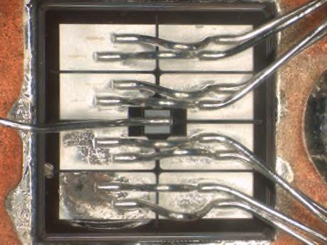
11 IGBT Module manufacturing : Card wire bonding Electrical contacting between electronic components and DBC substrates First bonding step: from DBC contact areas to electronic component Electrical tests of every single substrates Visual inspection under light microscope Wire bonding Single bonded substrates 11


12 IGBT Module manufacturing : System soldering Ensure proper adhesion and thermal contact between the DBC substrate and the baseplate for an efficient thermal dissipation Soldering on baseplate X-Ray inspection Soldering oven Assembly station Assembly principle X-ray unit Wired circuits soldered on base plates X-ray picture 12


13 IGBT Module manufacturing : System assembly Mounting of the frame onto the base plate Before After 13


14 IGBT Module manufacturing : Frame wire bonding Electrical contacting between DBC substrates and outer metallic leads on the frame Second bonding step: Frame connectors-to-dbc and DBC-to-DBC bonding - Bonding force, bonding time, ultrasonic energy - Shear force tests of bonds - Visual inspection of every modules power terminalsto-dbc bonds DBC-to- DBC bonds 14


15 IGBT Module manufacturing : Final assembly and testing Encapsulating, testing and packing for shipment Silicone potting - Control of the silicone-gel hardness 15

16 IGBT Module manufacturing : Final assembly and testing Gluing or clipping of the lid Electrical testing of every single module Bar code laser imprinting Final visual inspection Packing for shipment 16
17 Table of Contents 1 2 IGBT Module manufacturing process Failure Analysis process for IGBT module 17
18 FA(Failure Analysis) Process for IGBT Module


19 What is Failure Analysis? Determine how or why a semiconductor device has failed. Analyze failed products and clarify the failure causes and mechanism, and provide feedback to the manufacturing and design process not only to prevent reoccurrence in the future and but also to improve manufacturing and product quality. 19
20 General FA Process Flow for IGBT Modules Receiving Part arrival and registration Checking of the part returned and all necessary information provided FA Process Nondestructive analysis Destructive analysis External visual inspection X-ray inspection Electrical verification Scanning Acoustic Microscopy Mechanical/Chemical preparation Internal visual inspection Fault localization Cross-sectioning SEM/EDX analysis Reporting Report writing Report sending to customer 20


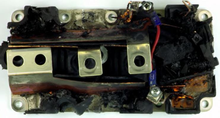
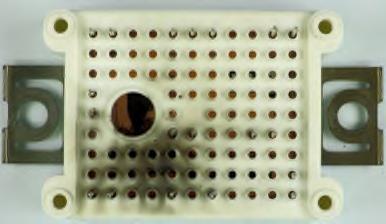
21 External Visual Inspection of Module Macrophotography Examples for modules at incoming inspection 21

22 Electrical Verification of Module Electrical measurements with curve tracers up to 5 kv Example shows blocking voltage curves of three systems of same module 22

23 Mechanical Preparation Removal of lid, frame, housing, power terminals Desoldering of DBC substrate and single dies 23


24 Chemical Preparation Removal of : - Silicone gel - Imide - Al - Cu - Oxides - Silicone gel removal before after Imide removal before after 24

25 Internal Visual Inspection(Optical Microscopy) 25
26 X-ray Inspection 26


27 Scanning Acoustic Microscopy Investigation of mechanical compounds < Substrate cracked > < System solder delamination > 27
")

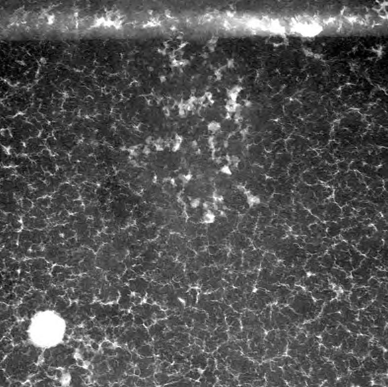
28 Fault Localization(Infrared Lock-In Thermography) <Observed hot spots on IGBTs> <Hot spot under bond wedges> 28

29 Cross-sectioning Si chip solder Artifact free cross section by ion beam milling Delamination Cracks 29


30 SEM and EDX analysis SEM surface inspection and scanning: Material analysis SEM image of a residual Al bond 30


31
Packaging Fault Isolation Using Lock-in Thermography
 Packaging Fault Isolation Using Lock-in Thermography Edmund Wright 1, Tony DiBiase 2, Ted Lundquist 2, and Lawrence Wagner 3 1 Intersil Corporation; 2 DCG Systems, Inc.; 3 LWSN Consulting, Inc. Addressing
Characterization of Flip Chip Interconnect Failure Modes Using High Frequency Acoustic Micro Imaging With Correlative Analysis
 Characterization of Flip Chip Interconnect Failure Modes Using High Frequency Acoustic Micro Imaging With Correlative Analysis Janet E. Semmens and Lawrence W. Kessler SONOSCAN, INC. 530 East Green Street
RAY S REWORK SECRETS TRAINING CERTIFICATION TEST (DVD-13C) v.3
 v.3") This test consists of twenty multiple-choice questions. All questions are from the video: Ray s Rework Secrets (DVD-13C). Each question has only one most correct answer. Circle the letter corresponding
This test consists of twenty multiple-choice questions. All questions are from the video: Ray s Rework Secrets (DVD-13C). Each question has only one most correct answer. Circle the letter corresponding
Extending Acoustic Microscopy for Comprehensive Failure Analysis Applications
 Extending Acoustic Microscopy for Comprehensive Failure Analysis Applications Sebastian Brand, Matthias Petzold Fraunhofer Institute for Mechanics of Materials Halle, Germany Peter Czurratis, Peter Hoffrogge
CHARACTERIZATION OF FLIP CHIP BUMP FAILURE MODES USING HIGH FREQUENCY ACOUSTIC MICRO IMAGING
 CHARACTERIZATION OF FLIP CHIP BUMP FAILURE MODES USING HIGH FREQUENCY ACOUSTIC MICRO IMAGING Janet E. Semmens and Lawrence W. Kessler SONOSCAN, INC. 530 East Green Street Bensenville, IL 60106 U.S.A. Tel:
Advanced Embedded Packaging for Power Devices
 2017 IEEE 67th Electronic Components and Technology Conference Advanced Embedded Packaging for Power Devices Naoki Hayashi, Miki Nakashima, Hiroshi Demachi, Shingo Nakamura, Tomoshige Chikai, Yukari Imaizumi,
B. Flip-Chip Technology
 B. Flip-Chip Technology B1. Level 1. Introduction to Flip-Chip techniques B1.1 Why flip-chip? In the development of packaging of electronics the aim is to lower cost, increase the packaging density, improve
Application Bulletin 240
 Application Bulletin 240 Design Consideration CUSTOM CAPABILITIES Standard PC board fabrication flexibility allows for various component orientations, mounting features, and interconnect schemes. The starting
CHAPTER 11: Testing, Assembly, and Packaging
 Chapter 11 1 CHAPTER 11: Testing, Assembly, and Packaging The previous chapters focus on the fabrication of devices in silicon or the frontend technology. Hundreds of chips can be built on a single wafer,
Chapter 11 Testing, Assembly, and Packaging
 Chapter 11 Testing, Assembly, and Packaging Professor Paul K. Chu Testing The finished wafer is put on a holder and aligned for testing under a microscope Each chip on the wafer is inspected by a multiple-point
ACOUSTIC MICRO IMAGING ANALYSIS METHODS FOR 3D PACKAGES
 ACOUSTIC MICRO IMAGING ANALYSIS METHODS FOR 3D PACKAGES Janet E. Semmens Sonoscan, Inc. Elk Grove Village, IL, USA Jsemmens@sonoscan.com ABSTRACT Earlier studies concerning evaluation of stacked die packages
MIL-STD-883E METHOD BOND STRENGTH (DESTRUCTIVE BOND PULL TEST)
") BOND STRENGTH (DESTRUCTIVE BOND PULL TEST) 1. PURPOSE. The purpose of this test is to measure bond strengths, evaluate bond strength distributions, or determine compliance with specified bond strength
BOND STRENGTH (DESTRUCTIVE BOND PULL TEST) 1. PURPOSE. The purpose of this test is to measure bond strengths, evaluate bond strength distributions, or determine compliance with specified bond strength
JUNE 2015 VOL 173 NO 6 TESTING TECHNOLOGIES ACOUSTIC MICROSCOPY P.18
 JUNE 2015 VOL 173 NO 6 TESTING TECHNOLOGIES ACOUSTIC MICROSCOPY P.18 2 18 TECHNICAL SPOTLIGHT ACOUSTIC IMAGING TECHNIQUES EFFECTIVELY MAP BURIED LAYER CONTOURS Acoustic microscopy advances enable mapping
PAGE 1/6 ISSUE Jul SERIES Micro-SPDT PART NUMBER R516 XXX 10X R 516 _ 1 0 _
 PAGE 1/6 ISSUE Jul-24-2017 SERIES Micro-SPDT PART NUMBER R516 XXX 10X R516 series: the RAMSES concept merges with the SLIM LINE technology, breaking up the frequency limits of SMT switches : - FULL SMT
High Power IGBT Module for Three-level Inverter
 High Power IGBT Module for Three-level Inverter Takashi Nishimura Takatoshi Kobayashi Yoshitaka Nishimura ABSTRACT In recent years, power conversion equipment used in the field of new energy and the field
UMS User guide for bare dies GaAs MMIC. storage, pick & place, die attach and wire bonding
 UMS User guide for bare dies GaAs MMIC storage, pick & place, die attach and wire bonding Ref. : AN00014097-07 Apr 14 1/10 Specifications subject to change without notice United Monolithic Semiconductors
Failure Analysis and manufacturing related customer complaints. Presented By- Anand
 Failure Analysis and manufacturing related customer complaints Presented By- Anand Date-15 Th sept 2007 What is Failure Analysis- Failure analysis is the investigation of the devices fails at customer
Standoff Height Measurement of Flip Chip Assemblies by Scanning Acoustic Microscopy
 Standoff Height Measurement of Flip Chip Assemblies by Scanning Acoustic Microscopy C.W. Tang, Y.C. Chan, K.C. Hung and D.P. Webb Department of Electronic Engineering City University of Hong Kong Tat Chee
MIL-STD-1580B REQUIREMENT 11 DETAILED REQUIREMENTS FOR CONNECTORS
 DETAILED REQUIREMENTS FOR CONNECTORS 11. General. This section describes detailed requirements for a DPA of commonly used connectors. These requirements supplement the general requirements in section 4.
Assembly Instructions for SCC1XX0 series
 Technical Note 82 Assembly Instructions for SCC1XX0 series TABLE OF CONTENTS Table of Contents...1 1 Objective...2 2 VTI's 32-lead Dual In-line Package (DIL-32)...2 3 DIL-32 Package Outline and Dimensions...2
Assembly Instructions for SCA6x0 and SCA10x0 series
 Technical Note 71 Assembly Instructions for SCA6x0 and SCA10x0 series TABLE OF CONTENTS Table of Contents...1 1 Objective...2 2 VTI'S DIL-8 and DIL-12 packages...2 3 Package Outline and Dimensions...2
High Resolution Backside Imaging and Thermography using a Numerical Aperture Increasing Lens
 High Resolution Backside Imaging and Thermography using a Numerical Aperture Increasing Lens Shawn A. Thorne, Steven B. Ippolito, Mesut G. Eraslan, Bennett B. Goldberg, and M. Selim Ünlü, Boston University,
Handling and Processing Details for Ceramic LEDs Application Note
 Handling and Processing Details for Ceramic LEDs Application Note Abstract This application note provides information about the recommended handling and processing of ceramic LEDs from OSRAM Opto Semiconductors.
PAGE 1/6 ISSUE SERIES Micro-SPDT PART NUMBER R516 XXX 10X. (All dimensions are in mm [inches]) R 516 _ 1 0 _
![PAGE 1/6 ISSUE SERIES Micro-SPDT PART NUMBER R516 XXX 10X. (All dimensions are in mm [inches]) R 516 _ 1 0 _](/thumbs/96/127769340.jpg "PAGE 1/6 ISSUE SERIES Micro-SPDT PART NUMBER R516 XXX 10X. (All dimensions are in mm [inches]) R 516 _ 1 0 _") PAGE 1/6 ISSUE 15-10-18 SERIES Micro-SPDT PART NUMBER R516 XXX 10X R516 series: the RAMSES concept merges with the SLIM LINE technology, breaking up the frequency limits of SMT switches : - FULL SMT TECHNOLOGY
PAGE 1/6 ISSUE 15-10-18 SERIES Micro-SPDT PART NUMBER R516 XXX 10X R516 series: the RAMSES concept merges with the SLIM LINE technology, breaking up the frequency limits of SMT switches : - FULL SMT TECHNOLOGY
2.8 Gen4 Medium Voltage SST Development
 2.8 Gen4 Medium Voltage SST Development Project Number Year 10 Projects and Participants Project Title Participants Institution Y10ET3 Gen4 Medium Voltage SST Development Yu, Husain NCSU 2.8.1 Intellectual
Hiding In Plain Sight. How Ultrasonics Can Help You Find the Smallest Bonded Wafer and Device Defects. A Sonix White Paper
 Hiding In Plain Sight How Ultrasonics Can Help You Find the Smallest Bonded Wafer and Device Defects A Sonix White Paper If You Can See It, You Can Solve It: Understanding Ultrasonic Inspection of Bonded
Features. Output Third Order Intercept (IP3) [2] dbm Power Added Efficiency %
![Features. Output Third Order Intercept (IP3) [2] dbm Power Added Efficiency %](/thumbs/84/89186722.jpg "Features. Output Third Order Intercept (IP3) [2] dbm Power Added Efficiency %") v5.1217 HMC187 2-2 GHz Typical Applications The HMC187 is ideal for: Test Instrumentation General Communications Radar Functional Diagram Features High Psat: +39 dbm Power Gain at Psat: +5.5 db High Output
v5.1217 HMC187 2-2 GHz Typical Applications The HMC187 is ideal for: Test Instrumentation General Communications Radar Functional Diagram Features High Psat: +39 dbm Power Gain at Psat: +5.5 db High Output
(HI80) Ultra-Precision High-Power High-Voltage Resistors. Token Electronics Industry Co., Ltd. Version: November 22, Web:
 Ultra-Precision High-Power High-Voltage Resistors. Token Electronics Industry Co., Ltd. Version: November 22, Web:") Version: November 22, 2017 (HI80) Ultra-Precision High-Power High-Voltage Resistors Token Electronics Industry Co., Ltd. Web: www.token.com.tw mailto: Taiwan: No.137, Sec. 1, Zhongxing Rd., Wugu District,
Version: November 22, 2017 (HI80) Ultra-Precision High-Power High-Voltage Resistors Token Electronics Industry Co., Ltd. Web: www.token.com.tw mailto: Taiwan: No.137, Sec. 1, Zhongxing Rd., Wugu District,
Instruction manual and data sheet ipca h
 1/15 instruction manual ipca-21-05-1000-800-h Instruction manual and data sheet ipca-21-05-1000-800-h Broad area interdigital photoconductive THz antenna with microlens array and hyperhemispherical silicon
CeraDiodes. Soldering directions. Date: July 2014
 CeraDiodes Soldering directions Date: July 2014 EPCOS AG 2014. Reproduction, publication and dissemination of this publication, enclosures hereto and the information contained therein without EPCOS' prior
Introduction to Manufacturing Processes
 Introduction to Manufacturing Processes Products and Manufacturing Product Creation Cycle Design Material Selection Process Selection Manufacture Inspection Feedback Typical product cost breakdown Manufacturing
Deliverable 4.2: TEM cross sections on prototyped Gated Resistors
 Deliverable 4.2: TEM cross sections on prototyped Gated Resistors Olga G. Varona, Geoff Walsh, Bernie Capraro Intel Ireland 21 June 2011 Abbreviation list D: drain FIB: focused ion-beam HRTEM: high resolution
(HI83) Thick Film Planar Dividers, High Voltage Resistors
 Thick Film Planar Dividers, High Voltage Resistors") Version: August 31, 2017 Electronics Tech. (HI83) Thick Film Planar Dividers, High Voltage Resistors Web: www.direct-token.com Email: rfq@direct-token.com Direct Electronics Industry Co., Ltd. China: 12F,
Version: August 31, 2017 Electronics Tech. (HI83) Thick Film Planar Dividers, High Voltage Resistors Web: www.direct-token.com Email: rfq@direct-token.com Direct Electronics Industry Co., Ltd. China: 12F,
General Rules for Bonding and Packaging
 General Rules for Bonding and Packaging at the Else Kooi Laboratory 3 CONTENT Rules for assembly at EKL 4 Introduction to assembly 5 Rules for Saw Lane 7 Rules for Chip Size 8 Rules for Bondpads 9 Rules
LAND AND CONDUCTOR REPAIR (DVD-97ABC)
") This test consists of twenty multiple-choice questions. All questions are from the video: Land and Conductor Repair (DVD-97ABC). Each question has only one most correct answer. Circle the letter corresponding
This test consists of twenty multiple-choice questions. All questions are from the video: Land and Conductor Repair (DVD-97ABC). Each question has only one most correct answer. Circle the letter corresponding
Ultrasonic Imaging of Microscopic Defects to Help Improve Reliability of Semiconductors and Electronic Devices
 7 Hitachi Review Vol. 65 (016), No. 7 Featured rticles Ultrasonic Imaging of Microscopic s to Help Improve Reliability of Semiconductors and Electronic Devices Scanning coustic Tomograph Kaoru Kitami Kaoru
Assembly/Packagng RF-PCB. Thick Film. Thin Film. Screening/Test. Design Manual
 Thick Film Thin Film RF-PCB Assembly/Packagng Screening/Test Design Manual RHe Design Manual The following rules are effective for the draft of circuit boards and hybrid assemblies. The instructions are
AN5046 Application note
 Application note Printed circuit board assembly recommendations for STMicroelectronics PowerFLAT packages Introduction The PowerFLAT package (5x6) was created to allow a larger die to fit in a standard
SUBJECT: PRECAUTIONS AND RECOMMENDATIONS FOR MITSUBISHI ELECTRIC SILICON RF POWER SEMICONDUCTORS GENERAL:
 APPLICATION NOTE Silicon RF Power Document NO. Date : 30 th May 2001 Rev. date : 22 th.jun. 2010 Prepared : K. Kajiwara T.Okawa Confirmed : T. Okawa (Taking charge of Silicon RF by MIYOSHI Electronics)
!"#$%&'()'*"+,+$&#' ' '
'*+,+$&#' ' '") !"#$%&'()'*"+,+$&#' *"89"+&+6'B22&83%45'8/6&10/%2'A"1'/22&83%4'/+#'C"0+0+D'8&67"#2'0+'&%&
!"#$%&'()'*"+,+$&#' *"89"+&+6'B22&83%45'8/6&10/%2'A"1'/22&83%4'/+#'C"0+0+D'8&67"#2'0+'&%&
TEM SAMPLE-PREPARATION PROCEDURES FOR THIN-FILM MATERIALS
 TEM SAMPLE-PREPARATION PROCEDURES FOR THIN-FILM MATERIALS Initial Set-Up: Heat up a hot plate to around 150-200 C Plan view Mounting/Grinding/Dimpling/Polishing: 1) Cleave a square-ish piece of sample.
SEMITOP Mounting instructions
 SEMITOP Mounting instructions ESD protection... 1 Temperature sensor... 1 Electrical isolation... 2 Heat sink specification... 2 Mounting surface... 3 Assembling Steps... 4 Thermal grease application...
Integration of Power, Control and Dynamic Braking in AC Motor Drives
 Thick Film & Hybrid Technology Integration of Power, Control and Dynamic Braking in AC Motor Drives Increased energy cost is undoubtedly one of the major problems facing industry today. Since almost every
RapidScan II Application Note General Composite Scanning
 RapidScan II Application Note General Composite Scanning RapidScan II General Composite Scanning Application Note Page 1 Applications The RapidScan system has been utilised for a wide range of inspections
Gold plating, 140 Gases compressed, 393 liquid,393 Grounding, safety, 403
 INDEX Acids, safety, 394 Activities, 1 Adhesives, 349 Allowances manufacturing, 77 rework,82 Aluminum Plating, 139 Analysis work distribution, 20, 29 processes, 32 Analyzing job details, 19 Assemblers
Capabilities of Flip Chip Defects Inspection Method by Using Laser Techniques
 Capabilities of Flip Chip Defects Inspection Method by Using Laser Techniques Sheng Liu and I. Charles Ume* School of Mechanical Engineering Georgia Institute of Technology Atlanta, Georgia 3332 (44) 894-7411(P)
Acoustic microscopy for 3D-SiP failure analysis
 Acoustic microscopy for 3D-SiP failure analysis Peter Czurratis PVA TePla Analytical Systems GmbH, Westhausen, Germany Sebastian Brand Fraunhofer Center for Applied Microstructure Diagnostics (CAM) Halle,
Application Notes. Introduction
 Introduction EMC Technology has provided an extensive collection of Application Notes that help designers mount and measure the products. These cover the complete line of Thermopads, Attenuators, SmartLoad,
High Efficient Heat Dissipation on Printed Circuit Boards. Markus Wille, R&D Manager, Schoeller Electronics Systems GmbH
 High Efficient Heat Dissipation on Printed Circuit Boards Markus Wille, R&D Manager, Schoeller Electronics Systems GmbH m.wille@se-pcb.de Introduction 2 Heat Flux: Q x y Q z The substrate (insulation)
Two major features of this text
 Two major features of this text Since explanatory materials are systematically made based on subject examination questions, preparation
Features: Applications:
 Water cooling UC 160 Gen2 UV LEDs Table of Contents Technology Overview...2 The advantages of COB Multi-chips-Package...2 Optical & Electrical Characteristics...3 Absolute Maximum Rating...4 Optical &
MICROELECTRONICS ASSSEMBLY TECHNOLOGIES. The QFN Platform as a Chip Packaging Foundation
 West Coast Luncheon January 15, 2014. PROMEX PROMEX INDUSTRIES INC. MICROELECTRONICS ASSSEMBLY TECHNOLOGIES The QFN Platform as a Chip Packaging Foundation 3075 Oakmead Village Drive Santa Clara CA Ɩ 95051
Part 5-1: Lithography
 Part 5-1: Lithography Yao-Joe Yang 1 Pattern Transfer (Patterning) Types of lithography systems: Optical X-ray electron beam writer (non-traditional, no masks) Two-dimensional pattern transfer: limited
Nondestructive Inspection of Underfill Layers Stacked up in Ceramics-Organics- Ceramics Packages with Scanning Acoustic Tomography (SAT)
") Nondestructive Inspection of Underfill Layers Stacked up in Ceramics-Organics- Ceramics Packages with Scanning Acoustic Tomography (SAT) Justin Zeng, Francoise Sarrazin, Jie Lian, Ph.D., Zhen (Jane) Feng,
Nondestructive Inspection of Underfill Layers Stacked up in Ceramics-Organics- Ceramics Packages with Scanning Acoustic Tomography (SAT) Justin Zeng, Francoise Sarrazin, Jie Lian, Ph.D., Zhen (Jane) Feng,
Theory and Applications of Frequency Domain Laser Ultrasonics
 1st International Symposium on Laser Ultrasonics: Science, Technology and Applications July 16-18 2008, Montreal, Canada Theory and Applications of Frequency Domain Laser Ultrasonics Todd W. MURRAY 1,
FLASHSOLDERING UPDATE EXTENDING FINE MAGNET WIRE JOINING APPLICATIONS
 FLASHSOLDERING UPDATE EXTENDING FINE MAGNET WIRE JOINING APPLICATIONS David W. Steinmeier microjoining Solutions & Mike Becker Teka Interconnection Systems Abstract: FlashSoldering was first developed
Solar Panels Build Your Own Instructions for the Do It Yourself Person Let s have some fun!
 Solar Panels Build Your Own Instructions for the Do It Yourself Person Let s have some fun! Before we get started lets talk about a few things like materials and tools. Let s start off with tools as Lowes
Solutions for High Power Applications
 C U S T O M D E S I G N E D P O W E R M O D U L E S Solutions for High Power Applications C U S T O M D E S I G N E D P O W E R M O D U L E S High Power Solutions in Custom Module Design Powerex has addressed
Chip Assembly on MID (Molded Interconnect Device) A Path to Chip Modules with increased Functionality
 A Path to Chip Modules with increased Functionality") T e c h n o l o g y Dr. Werner Hunziker Chip Assembly on MID (Molded Interconnect Device) A Path to Chip Modules with increased Functionality The MID (Molded Interconnect Device) technology enables the
T e c h n o l o g y Dr. Werner Hunziker Chip Assembly on MID (Molded Interconnect Device) A Path to Chip Modules with increased Functionality The MID (Molded Interconnect Device) technology enables the
WB/WT/WXSC 250µm/WLSC100µm - Assembly by Wirebonding
 General description This document describes the attachment techniques recommended by Murata* for their vertical capacitors on the customer substrates. This document is non-exhaustive. Customers with specific
EFFECTS OF USG CURRENT AND BONDING LOAD ON BONDING FORMATION IN QFN STACKED DIE PACKAGE. A. Jalar, S.A. Radzi and M.A.A. Hamid
 Solid State Science and Technology, Vol. 16, No 2 (2008) 65-71 EFFECTS OF USG CURRENT AND BONDING LOAD ON BONDING FORMATION IN QFN STACKED DIE PACKAGE A. Jalar, S.A. Radzi and M.A.A. Hamid School of Applied
Composite Thermal Damage Measurement with Handheld FTIR. April 9, 2013 Brian D. Flinn, Ashley Tracey, and Tucker Howie University of Washington
 Composite Thermal Damage Measurement with Handheld FTIR April 9, 2013 Brian D. Flinn, Ashley Tracey, and Tucker Howie University of Washington Composite Thermal Damage Measurement with Handheld FTIR Motivation
Failure Analysis Report
 High Quality FA and Reliability Testing Company 1719 S. Grand Ave Santa Ana, CA 92705-4808 Tel: 949-329-0340 Website: www.icfailureanalysis.com Failure Analysis Report ICFA Lab Reference Number: ICFA-0003
Line-Following Robot
 1 Line-Following Robot Printed Circuit Board Assembly Jeffrey La Favre October 5, 2014 After you have learned to solder, you are ready to start the assembly of your robot. The assembly will be divided
Click here. For machines from 2009 onward; Batch No. 08N2505 or later (PO No or later & PO No. s ending in -EU): (Model No.
: (Model No.") For machines from 2009 onward; Batch No. 08N2505 or later (PO No. 95333 or later & PO No. s ending in -EU): (Model No. -B) Click here (Model No. ) Click here 1 P a g e For machines from 2009 onward; Batch
For machines from 2009 onward; Batch No. 08N2505 or later (PO No. 95333 or later & PO No. s ending in -EU): (Model No. -B) Click here (Model No. ) Click here 1 P a g e For machines from 2009 onward; Batch
RF Hybrid Linear Amplifier Using Diamond Heat Sink
 RF Hybrid Linear Amplifier Using Diamond Heat Sink Item Type text; Proceedings Authors Karabudak, Nafiz Publisher International Foundation for Telemetering Journal International Telemetering Conference
Characterization of Prototypes
 5 Characterization of Prototypes 5.1 Assessment of Prototype Performance The assessment of the HIGHTECS prototype parts has covered the following components: ASIC in PGA Package Hybrid Circuit High Temperature
Component Package Decapsulation Process with Analogue Signature Analysis Support
 Component Package Decapsulation Process with Analogue Signature Analysis Support NEUMANN PETR, ADAMEK MILAN, SKOCIK PETR Faculty of Applied Informatics Tomas Bata University in Zlin nam.t.g.masaryka 5555
The performance of a Pre-Processor Multi-Chip Module for the ATLAS Level-1 Trigger
 The performance of a Pre-Processor Multi-Chip Module for the ATLAS Level-1 Trigger J. Krause, U. Pfeiffer, K. Schmitt, O. Stelzer Kirchhoff-Institut für Physik, Universität Heidelberg, Germany Abstract
Tape Automated Bonding
 Tape Automated Bonding Introduction TAB evolved from the minimod project begun at General Electric in 1965, and the term Tape Automated Bonding was coined by Gerard Dehaine of Honeywell Bull in 1971. The
Chapter 3 Fabrication
 Chapter 3 Fabrication The total structure of MO pick-up contains four parts: 1. A sub-micro aperture underneath the SIL The sub-micro aperture is used to limit the final spot size from 300nm to 600nm for
Enameled Wire Having Polyimide-silica Hybrid Insulation Layer Prepared by Sol-gel Process
 Journal of Photopolymer Science and Technology Volume 28, Number 2 (2015) 151 155 2015SPST Enameled Wire Having Polyimide-silica Hybrid Insulation Layer Prepared by Sol-gel Process Atsushi Morikawa 1,
16SCT000 TRANSFORMER-COUPLED MOSFET / IGBT GATE DRIVER 16SCT000 - PRELIMINARY SPECIFICATION - REVISION MAY 29, 2017
 Maximum Voltage... 30 V Transformer Drive provides HV isolation No other external components required Fast IGBT Turn-On & Turn-Off Times DIE (TOP VIEW) Description The 16SCT000 is an IGBT/MOSFET gate driver
23. Packaging of Electronic Equipments (2)
") 23. Packaging of Electronic Equipments (2) 23.1 Packaging and Interconnection Techniques Introduction Electronic packaging, which for many years was only an afterthought in the design and manufacture of
23. Packaging of Electronic Equipments (2) 23.1 Packaging and Interconnection Techniques Introduction Electronic packaging, which for many years was only an afterthought in the design and manufacture of
Fabrication of High-Voltage Bridge Rectifier Modules for Pulse Power Applications
 Fabrication of High-Voltage Bridge Rectifier Modules for Pulse Power Applications by Dimeji Ibitayo, Gail Koebke, Damian Urciuoli, and C Wesley Tipton ARL-MR-0877 September 2014 Approved for public release;
Integrated diodes. The forward voltage drop only slightly depends on the forward current. ELEKTRONIKOS ĮTAISAI
 1 Integrated diodes pn junctions of transistor structures can be used as integrated diodes. The choice of the junction is limited by the considerations of switching speed and breakdown voltage. The forward
Yole Developpement. Developpement-v2585/ Publisher Sample
 Yole Developpement http://www.marketresearch.com/yole- Developpement-v2585/ Publisher Sample Phone: 800.298.5699 (US) or +1.240.747.3093 or +1.240.747.3093 (Int'l) Hours: Monday - Thursday: 5:30am - 6:30pm
Inspection Method Sheet
 Inspection Method Sheet Part Number: Generic Part Name: PCB Filters Drawing Number: Generic Operation: In Process / Final Page 1 of 10 Written By: Myra Cope Doc. #: TT-PC-0378 Rev. 14 Date: 10-15-08 Applicable
1. Initial Precautions 2. Technical Precautions and Suggestions 3. General Information and Cure Stages 4. Understanding and Controlling Cure Time
 How to apply Arctic Silver Premium Thermal Adhesive 1. Initial Precautions 2. Technical Precautions and Suggestions 3. General Information and Cure Stages 4. Understanding and Controlling Cure Time 5.
TO10 TO20 TBD. LED Module CSP Spot Tunable. Samsung spot tunable is reasonable solution with compact size using Samsung CSP and good compatibility.
 Product Family Datasheet Sheet Rev_0.4 Rev.0.0 2016.11.10 5. 9 1 LED Module CSP Spot Tunable TO10 TO20 Samsung spot tunable is reasonable solution with compact size using Samsung CSP and good compatibility.
Effect of stainless steel chemical composition on brazing ability of filler metal
 IOP Conference Series: Materials Science and Engineering OPEN ACCESS Effect of stainless steel chemical composition on brazing ability of filler metal To cite this article: Yasuyuki Miyazawa et al 2014
(HI80M) Tubular High Voltage Precision Divider Resistors. Token Electronics Industry Co., Ltd. Version: July 16, Web:
 Tubular High Voltage Precision Divider Resistors. Token Electronics Industry Co., Ltd. Version: July 16, Web:") Version: July 16, 2018 (HI80M) Tubular High Voltage Precision Divider Resistors Token Electronics Industry Co., Ltd. Web: www.token.com.tw mailto: Taiwan: No.137, Sec. 1, Zhongxing Rd., Wugu District,
Version: July 16, 2018 (HI80M) Tubular High Voltage Precision Divider Resistors Token Electronics Industry Co., Ltd. Web: www.token.com.tw mailto: Taiwan: No.137, Sec. 1, Zhongxing Rd., Wugu District,
Makrolon Solid Polycarbonate Sheets
 1. General remarks Tools sheets can be machined using the standard tools commonly used for metal and woodworking. We recommend carbide-tipped tools. Above all, it is important to use sharp cutting tools
CERTIFICATE OF ACCREDITATION
 CERTIFICATE OF ACCREDITATION ANSI-ASQ National Accreditation Board/ACLASS 500 Montgomery Street, Suite 625, Alexandria, VA 22314, 877-344-3044 This is to certify that Evans Analytical Group, LLC 15 Morgan
EPE 2005 Dresden ESCAPEE. ESCAPEE Project. SiC Workshop. EPE 2005, September 12
 1 EPE 2005 Dresden ESCAPEE 2 The achievements of the EC funded project "Establish Silicon Carbide Applications for Power Electronics in Europe" (ESCAPEE) J. Millan 1, P. Godignon 1, D. Tournier 1, P.A.
MIL-STD-883H METHOD ULTRASONIC INSPECTION OF DIE ATTACH
 * ULTRASONIC INSPECTION OF DIE ATTACH 1. PURPOSE. The purpose of this examination is to nondestructively detect unbonded regions, delaminations and/or voids in the die attach material and at interfaces
Introduction to Wire-Bonding
 Introduction to Wire-Bonding Wire bonding is a kind of friction welding Material are connected via friction welding Advantage: Different materials can be connected to each other widely used, e.g. in automobile
unit 3: GENErAL ElectriCAL SySTEM DiAGNOSiS
 Electrical/Electronic Systems unit 3: GENErAL ElectriCAL SySTEM DiAGNOSiS lesson 4: wire and connector repairs I. Connector repairs A. Connector repairs involve fixing damaged wires. Wires are marred due
SPECIFICATION FOR APPROVAL 1/8W 0816 LOW RESISTNACE CHIP RESISTOR
 PAGE : 1 OF 11 1/8W 0816 LOW RESISTNACE CHIP RESISTOR 1. Scope This specification applies to 0.8mm x 1.60mm size 1/8W, fixed metal film chip resistors rectangular type for use in electronic equipment.
Transistor was first invented by William.B.Shockley, Walter Brattain and John Bardeen of Bell Labratories. In 1961, first IC was introduced.
 Unit 1 Basic MOS Technology Transistor was first invented by William.B.Shockley, Walter Brattain and John Bardeen of Bell Labratories. In 1961, first IC was introduced. Levels of Integration:- i) SSI:-
33-47 GHz Wide Band Driver Amplifier TGA4522
 33-47 GHz Wide Band Driver Amplifier Key Features Frequency Range: 33-47 GHz 27.5 dbm Nominal Psat @ 38GHz 27 dbm P1dB @ 38 GHz 36 dbm OTOI @ Pin = 19 dbm/tone 18 db Nominal Gain @ 38GHz db Nominal Return
All-SiC Modules Equipped with SiC Trench Gate MOSFETs
 All-SiC Modules Equipped with SiC Trench Gate MOSFETs NAKAZAWA, Masayoshi * DAICHO, Norihiro * TSUJI, Takashi * A B S T R A C T There are increasing expectations placed on products that utilize SiC modules
Round-040D Round-050D Round-060D
 Product Family Data Sheet Rev.4.1 2015. 9.16 1# LED Module Down Light Series Round-040D Round-050D Round-060D Samsung Down-Light Modules enable 4inch to 8inch down light design with better uniformity and
Process Certification and Defect Recognition: Hybrids, Microcircuits and RF/MMIC Modules (3 DAYS)
") Process Certification and Defect Recognition: Hybrids, Microcircuits and RF/MMIC Modules (3 DAYS) Course Description: Most companies struggle to introduce new lines and waste countless manhours and resources
Process Certification and Defect Recognition: Hybrids, Microcircuits and RF/MMIC Modules (3 DAYS) Course Description: Most companies struggle to introduce new lines and waste countless manhours and resources
High-power IGBT Modules
 High-power IGBT Modules Takashi Nishimura Yoshikazu Takamiya Osamu Nakajima 1. Introduction To help curb global warming, clean energy, rather than fossil fuels, has been used increasingly in recent years.
Handling and Processing Details for Ceramic LEDs Application Note
 Handling and Processing Details for Ceramic LEDs Application Note Abstract This application note provides information about the recommended handling and processing of ceramic LEDs from OSRAM Opto Semiconductors.
SCANNING ELECTRON MICROSCOPE (SEM) INSPECTION OF SEMICONDUCTOR DICE. ESCC Basic Specification No
 INSPECTION OF SEMICONDUCTOR DICE. ESCC Basic Specification No") Page 1 of 24 SCANNING ELECTRON MICROSCOPE (SEM) INSPECTION OF SEMICONDUCTOR DICE ESCC Basic Specification Issue 2 February 2014 Document Custodian: European Space Agency see https://escies.org PAGE 2 LEGAL
Page 1 of 24 SCANNING ELECTRON MICROSCOPE (SEM) INSPECTION OF SEMICONDUCTOR DICE ESCC Basic Specification Issue 2 February 2014 Document Custodian: European Space Agency see https://escies.org PAGE 2 LEGAL
Murata Silicon Capacitors WBSC / WTSC / WXSC 250 µm / WLSC 100 µm Assembly by Wirebonding. Table of Contents
 Table of Contents Table of Contents...1 Introduction...2 Handling Precautions and Storage...2 Pad Finishing...2 Process Flow with Glue...2 Process Flow with Solder Paste...3 Recommendations concerning
How to Hand Solder an Electric Wire to a COB LED
 How to Hand Solder an Electric Wire to a COB LED Table of Contents 1. Overview 2. Necessary/Recommended Soldering Equipment 3. How to Choose the Optimal Soldering Iron Tip 4. Cautions/Suggestions for Stripping
PHGN/CHEN/MLGN 435/535: Interdisciplinary Silicon Processing Laboratory. Simple Si solar Cell!
 Where were we? Simple Si solar Cell! Two Levels of Masks - photoresist, alignment Etch and oxidation to isolate thermal oxide, deposited oxide, wet etching, dry etching, isolation schemes Doping - diffusion/ion