查询 TB6560FG 供应商捷多邦, 专业 PCB 打样工厂,24 小时加急出货 TB6560HQ,TB6560FG
|
|
|
- Madeline Curtis
- 5 years ago
- Views:
Transcription

 = 0.6 Ω (typ.")
1 1 查询 TB6560FG 供应商捷多邦, 专业 PCB 打样工厂,24 小时加急出货 Preliminary TOSHIBA BiCD Integrated Circuit Silicon Monolithic TB6560HQ,TB6560FG PWM Chopper-Type bipolar Stepping Motor Driver IC The is a PWM chopper-type sinusoidal micro-step bipolar stepping motor driver IC. It supports both 2-phase/1-2-phase/W1-2-phase/2W1-2-phase excitation mode and forward/reverse mode and is capable of low-vibration, high-performance drive of 2-phase bipolar type stepping motors using only a clock signal. TB6560HQ Features Single-chip bipolar sinusoidal micro-step stepping motor driver Uses high withstand voltage BiCD process: Ron (upper lower) = 0.6 Ω (typ.) Forward and reverse rotation control available Selectable phase drive (2, 1-2, W1-2, and 2W1-2) High output withstand voltage: V CEO = 40 V High output current: I OUT = HQ: 3.5 A (peak) FG: 2.5 A (peak) Packages: HZIP25-P-1.27/HQFP64-P Built-in input pull-down resistor: 100 kω (typ.) Output monitor pin equipped: MO current (I MO (max) = 1 ma) Equipped with reset and enable pins Built-in overheat protection circuit TB6560FG Weight: HZIP25-P-1.27: 9.86 g (typ.) HQFP64-P : 0.26 g (typ.) The is a Pb-free product. The following conditions apply to solderability: *Solderability 1. Use of Sn-63Pb solder bath *solder bath temperature = 230 C *dipping time = 5 seconds *number of times = once *use of R-type flux 2. Use of Sn-3.0Ag-0.5Cu solder bath *solder bath temperature = 245 C *dipping time = 5 seconds *the number of times = once *use of R-type flux *: Since this product has a MOS structure, it is sensitive to electrostatic discharge. These ICs are highly sensitive to electrostatic discharge. When handling them, please be careful of electrostatic discharge, temperature and humidity conditions.
2 2 Block Diagram V DD Protect M O V MA 20/30, 31 19/28 17/23 18/25, 26 M1 M2 23/36 22/35 Decoder Bridge driver A OUT_AP 16/19, 20 13/10, 11 CW/CCW 21/33 Overheat protection circuit OUT_AM CLK RESET 3/45 5/48 Input circuit selector circuit A + N FA 14/13, 14, 15 ENABLE 4/47 8/55, 56 V MB DCY1 DCY2 25/39 24/38 Decoder Bridge driver B B OUT_BP 12/6, 7 9/61, 62 OSC 7/53 OSC OUT_BM selector circuit B + 11/2, 3, 4 N FB Maximum current setting circuit 2/43 1/42 6/50, 51 15/16 10/1 TQ1 TQ2 SGND PGNDA PGNDB TB6560HQ/TB6560FG
3 3 Pin Functions HQ Pin No. FG I/O Symbol Functional Description 1 42 Input TQ2 Torque setting input (current setting) (built-in pull-down resistor) 2 43 Input TQ1 Torque setting input (current setting) (built-in pull-down resistor) 3 45 Input CLK Step transition, clock input (built-in pull-down resistor) 4 47 Input ENABLE H: Enable; L: All output OFF (built-in pull-down resistor) 5 48 Input RESET L: Reset (output is reset to its initial state) (built-in pull-down resistor) 6 50/51 SGND Signal ground (control side) (Note 1) 7 53 OSC Connects to and oscillates CR. Output chopping. 8 55/56 Input V MB Motor side power pin (B phase side) (Note 1) 9 61/62 Output OUT_BM OUT_B output (Note 1) 10 1 PGNDB Power ground 11 2/3/4 N FB B channel output current detection pin (resistor connection). Short the two pins for FG. (Note 1) 12 6/7 Output OUT_BP OUT_B output (Note 1) 13 10/11 Output OUT_AM OUT_A output (Note 1) 14 13/14/15 N FA PGNDA Power ground A channel output current detection pin (resistor connection). Short the two pins for FG. (Note 1) 16 19/20 Output OUT_AP OUT_A output (Note 1) Output M O Initial state detection output. ON when in initial state (open drain) /26 Input V MA Motor side power pin (A phase side) (Note 1) Output Protect When TSD, ON (open drain). Normal Z /31 Input V DD Control side power pin. (Note 1) Input CW/CCW Forward/Reverse toggle pin. L: Forward; H: Reverse (built-in pull-down resistor) Input M2 Excitation mode setting input (built-in pull-down resistor) Input M1 Excitation mode setting input (built-in pull-down resistor) Input DCY2 Decay mode setting input (built-in pull-down resistor) Input DCY1 Decay mode setting input (built-in pull-down resistor) HQ: No Non-connection (NC) FG: Other than the above pins, all are NC (Since NC pins are not connected to the internal circuit, a potential can be applied to those pins.) All control input pins: Pull-down resistor 100 kω (typ.) Note 1: If the FG pin number column indicates more than one pin, the indicated pins should be tied to each other at a position as close to the pins as possible. (The electrical characteristics of the relevant pins in this document refer to those when they are handled in that way.) <Terminal circuits> Input pins (M1, M2, CLK, CW/CCW, ENABLE and RESET) Output ins (MO, PROTECT) V DD 100 Ω 100 Ω 100 kω
4 4 Absolute Maximum Ratings (Ta = 25 C) Characteristic Symbol Rating Unit Power supply voltage V DD 6 V MA/B 40 V Output current Peak HQ I O (PEAK) 3.5 FG 2.5 A/phase MO drain current I (MO) 1 ma Input voltage V IN 5.5 V Power dissipation HQ FG P D 5 (Note 1) 43 (Note 2) 1.7 (Note 3) 4.2 (Note 4) Operating temperature T opr 30 to 85 C Storage temperature T stg 55 to 150 C Note 1: Ta = 25 C, No heat sink. Note 2: Ta = 25 C, with infinite heat sink (HZIP25). Note 3: Ta = 25 C, with soldered leads. Note 4: Ta = 25 C, when mounted on the board (4-layer board). Susceptible to the board layout and the mounting conditions. W Operating Range (Ta = 20 to 85 C) Power supply voltage Output current Characteristic Symbol Test Condition Min Typ. Max Unit V DD V V MA/B V MA/B > = V DD V HQ 3 I OUT FG 1.5 Input voltage V IN V Clock frequency f CLK 15 khz OSC frequency f OSC 600 khz A
5 5 Electrical Characteristics (Ta = 25 C, V DD = 5 V, V M = 24 V) Characteristic Symbol Test Circuit Test Condition Min Typ. Max Unit High V IN (H) 2.0 V DD Input voltage 1 M1, M2, CW/CCW, CLK, RESET, V Low V IN (L) ENABLE, DECAY, TQ1, TQ2, ISD Input hysteresis voltage V H mv Input current Consumption current V DD pin Consumption current V M pin I IN (H) 1 ENABLE, DECAY, TQ1, TQ2, ISD V IN = 5.0 V Built-in pull-down resistor M1, M2, CW/CCW, CLK, RESET, I IN (L) V IN = 0 V 1 Output open, I DD1 RESET : H, ENABLE: H 3 5 (2, 1-2 phase excitation) I DD2 Output open, RESET : H, ENABLE: H (W1 2, 2W1-2 phase excitation) 3 5 I DD3 RESET : L, ENABLE: L 2 5 I DD4 1 RESET : H, ENABLE: L 2 5 I M1 1 RESET : H/L, ENABLE: L I M2 RESET : H/L, ENABLE: H Output channel margin of error V O B/A, C OSC = µf 5 5 % V level Level differential V HH TQ1 = H, TQ2 = H V HL TQ1 = L, TQ2 = H V LH TQ1 = H, TQ2 = L V LL TQ1 = L, TQ2 = L 100 Minimum clock pulse width t W (CLK) 100 ns MO output residual voltage V OL MO I OL = 1 ma 0.5 V TSD TSD (Design target value) 170 C TSD hysteresis TSDhys (Design target value) 20 C Oscillating frequency f OSC C = 330 pf khz µa ma ma %
6 6 Electrical Characteristics (Ta = 25 C, V DD = 5 V, V M = 24 V) Output Block Output ON resistor A-B chopping current (Note) 2W1-2- phase excitation 2W1-2- phase excitation 2W1-2- phase excitation 2W1-2- phase excitation 2W1-2- phase excitation 2W1-2- phase excitation 2W1-2- phase excitation 2W1-2- phase excitation Characteristic W1-2- phase excitation HQ FG 1-2- phase excitation Symbol Test Circuit Test Condition Min Typ. Max Unit Ron U1H I OUT = 1.5 A Ron L1H Ron U1F I OUT = 1.5 A Ron L1F θ = θ = 1/ W1-2- phase excitation θ = 2/ θ = 3/ W1-2- phase excitation 1-2- phase excitation TQ1 = L, TQ2 = L θ = 4/ θ = 5/ W1-2- phase excitation 2-phase excitation Vector θ = 6/ θ = 7/ Reference voltage V Output transistor switching characteristics Delay time Output leakage current Note: Maximum current (θ = 0): 100% TQ1, TQ2 = L (100%) OSC = 100 khz 100 Ω % mv t f C L = 15 pf 0.1 t r R L = 2 Ω, V = 0 V, 0.1 t plh 7 RESET to output 0.1 t plh ENABLE to output 0.3 t phl 0.2 Upper side I LH 6 V M = 40 V 1 Lower side I LL 1 µs µa
7 7 Description of Functions 1. Excitation s You can use the M1 and M2 pin settings to configure four different excitation settings. (The default is 2-phase excitation using the internal pull-down.) M2 Input M1 Mode (Excitation) L L 2-phase L H 1-2-phase H L W1-2-phase H H 2W1-2-phase 2. Function When the ENABLE signal goes Low level, it sets an OFF on the output. The output changes to the Initial mode shown in the table below when the RESET signal goes Low level. In this mode, the status of the CLK and CW/CCW pins are irrelevant. Input CLK CW/CCW RESET ENABLE L H H CW H H H CCW Output Mode X X L H Initial mode X X X L Z X: Don t care 3. Initial Mode When RESET is used, the phase currents are as follows. In this instance, the MO pin is L (connected to open drain). Excitation Mode A Phase B Phase 2-phase 100% 100% 1-2-phase 100% 0% W1-2-phase 100% 0% 2W1-2-phase 100% 0% 4. Decay s Output is generated by four PWM blasts; 25% decay is created by inducing decay during the last blast in Fast mode; 50% decay is created by inducing decay during the last two blasts in Fast mode; and 100% decay is created by inducing all four blasts in Fast mode. If there is no input with the pull-down resistor connection then the setting is Normal. Dcy2 Dcy1 Decay L L Normal 0% L H 25% Decay H L 50% Decay H H 100% Decay
8 8 5. Torque s ( ) The current ratio used in actual operations is determined in regard to the current setting due to resistance. Configure this for extremely low torque scenarios such as when Weak Excitation mode is stopped. If there is no input with the pull-down resistor connection then the setting is 100% torque. TQ2 TQ1 Ratio L L 100% L H 75% H L 50% H H 20% (weak excitation) 6. Protect and MO (Output Pins) You can configure settings from the receiving side by using an open-drain connection for the output pins and making the pull-up voltage variable. When a given pin is in its designated state it will go ON and output at Low level. Pin State Protect MO Low Overheat protection operation Initial state Z Normal operation Other than initial state Open-drain connection 7. OSC Output chopping waves are generated by connecting the condenser and having the CR oscillate. The values are as shown below (roughly: ± 30% margin of error). Condenser Oscillating Frequency 1000 pf 44 khz 330 pf 130 khz 100 pf 400 khz
9 9 Relationship between Enable, RESET and Output (OUT and MO) Ex-1: ENABLE 1-2-Phase Excitation (M1: H, M2: L) CW CLK ENABLE RESET MO (%) I A t 0 t 1 t 2 t 3 OFF t 7 t 8 t 9 t 10 t 11 t 12 The ENABLE signal at Low level disables only the output signals. Internal logic functions proceed in accordance with input clock signals and without regard to the ENABLE signal. Therefore output current is initiated by the timing of the internal logic circuit after release of disable mode. Ex-2: RESET 1-2-Phase Excitation (M1: H, M2: L) CLK CW ENABLE RESET MO (%) I A t 0 t 1 t 2 t 3 t 2 t 3 t 4 t 5 t 6 t 7 t 8 When the RESET signal goes Low level, output goes Initial state and the MO output goes Low level (Initial state: A Channel output current is 100%). Once the RESET signal returns to High level, output continues from the next state after Initial from the next raise in the Clock signal.
10 10 2-Phase Excitation (M1: L, M2: L, CW Mode) CW CLK MO (%) 100 I A (%) 100 I B t 0 t 1 t 2 t 3 t 4 t 5 t 6 t Phase Excitation (M1: H, M2: L, CW Mode) CLK CW MO (%) I A (%) I B t 0 t 1 t 2 t 3 t 4 t 5 t 6 t 7 t 8
11 11 W1-2-Phase Excitation (M1: L, M2: H, CW Mode) CW CLK MO (%) I A (%) I B t 0 t 1 t 2 t 3 t 4 t 5 t 6 t 7 t 8 t 9 t 10 t 11 t 12 t 13 t 14 t 15 t 16
12 12 2W1-2-Phase Excitation (M1: H, M2: H, CW Mode) CW CLK MO (%) I A (%) I B t 0 t 1 t 2 t 3 t 4 t 5 t 6 t 7 t 8 t 9 t 10 t 11 t 12 t 13 t 14 t 15 t 16 t 17 t 18 t 19 t 20 t 21 t 22 t 23 t 24 t 25 t 26 t 27 t 28 t 29 t 30 t 31 t 32
13 13 <Input Signal Example> CK MO M1 M2 RESET (%) I A phase excitation W1-2-phase excitation It is recommended that M1 and M2 signals be changed after setting the RESET signal Low during the Initial state (MO is Low). Even when the MO is Low, changing the RESET signal without setting the RESET signal Low may cause the discontinuity in the current waveform.
14 14 1. Waveform and s of Mixed Decay Mode You can configure the points of the current s shaped width (current s pulsating flow) using 1-bit input in Decay mode for constant-current control. refers to the point at which the output current reaches its setting current value and refers to the monitoring timing of the setting current. The smaller the MDT value, the smaller the current ripple (current wave peak), and the current s decay capability will fall. OSC Pin Internal Waveform Normal Mode Charge mode : current value reached Slow mode monitoring (When setting current value > Output current) Charge mode 25% Decay Mode MDT Charge mode : current value reached Slow mode Mixed decay timing Fast mode monitoring (When setting current value > Output current) Charge mode 50% Decay Mode MDT Charge mode : current value reached Slow mode Mixed decay timing Fast mode monitoring (When setting current value > Output current) Charge mode 100% Decay Mode Charge mode : current value reached Fast mode monitoring (When setting current value > Output current) Charge mode
15 15 2. Control Modes (Decay Mode effect) Direction in which current value increases (sine wave) Charge Slow Fast Charge Slow Fast Charge Slow Fast Charge Slow Fast Direction in which sine wave decreases (when a high decay ratio (MDT%) is used in Mixed Decay mode) Slow Slow Since the current s rate of decay is fast, its compliance with the setting current value is also fast. Charge Fast Charge Fast Slow Slow Fast Charge Fast Direction in which sine wave decreases (when a low decay ratio (MDT%) is used in Mixed Decay mode) Since the current s rate of decay is slow, its compliance with the setting current value takes a long time (or may not follow at all). Slow Slow Charge Fast Charge Fast Slow Fast Slow Fast During Mixed Decay mode and Fast Decay mode, if the setting current value < output current at : current monitoring point, the Charge mode at the next chopping cycle will disappear and the pattern will change to Slow Fast Mode (Slow Fast occurs at MDT). (In reality, a charge is applied momentarily to confirm the current.) Note: These figures are intended for illustrative purposes only. If designed more realistically, they would show transient response curves.
16 16 3. Mixed Decay Mode Waveform ( Waveform) OSC Pin Internal Waveform I OUT 25% Mixed Decay Mode MDT (Mixed Decay Timing) Points When the points come after mixed decay timing Switches to Fast mode after Charge mode I OUT current value MDT (Mixed Decay Timing) Points 25% Mixed Decay Mode CLK Signal Input When the output current value > current value in mixed decay mode I OUT 25% MIXED DECAY MODE MDT (Mixed Decay Timing) Points CLK Signal Input *: Even if the output current rises above the setting current at the point, a charge is applied momentarily to confirm the current.
17 17 4. Fast Decay Mode Waveform After the current value set by, torque or other means is attained, the output current to load will make the transition to full regenerative mode. I OUT Transition to Charge mode for a brief moment Fast Decay Mode (100% Decay Mode) Since the setting current value > output current, charge mode Fast Decay mode transition will take place at even the next cycle. CLK Signal Input
18 18 5. CLK Signal and Internal CR CK Output Waveform (when the CLK signal is input in the middle of Slow mode) 25% Mixed Decay Mode OSC Pin Internal Waveform I OUT MDT MDT CLK Signal Input Transition to Charge mode for a brief moment The CR counter is reset here. When the CLK signal is input, the Chopping Counter (OSC Counter) is forcibly reset at the timing of the OSC. As a result, the response to input data is fast in comparison to methods that don t reset the counter. The delay time is one OSC cycle: 10 khz Chopping using the Logic Block logic value. After the OSC Counter is reset by CLK signal input, the transition is invariably made to Charge mode for a brief moment to compare the current. Note: Even in Fast Decay Mode, the transition is invariably made to Charge mode for a brief moment to compare the current.
19 19 6. CLK Signal and Internal OSC Output Waveform (when the CLK signal is input in the middle of Charge mode) 25% Mixed Decay Mode OSC Pin Internal Waveform MDT I OUT MDT CLK Signal Input Transition to Charge mode for a brief moment The OSC Counter is reset here.
20 20 7. CLK Signal AND Internal OSC Output Waveform (when the CLK signal is input in the middle of Fast mode) 25% Mixed Decay Mode OSC Pin Internal Waveform I OUT MDT MDT CLK Signal Input Transition to Charge mode for a brief moment The OSC Counter is reset here.
21 21 8. Internal OSC Output Waveform when is Reverse (when the CLK signal is input using 2-phase excitation) 25% Mixed Decay Mode I OUT 0 MDT CLK Signal Input The OSC Counter is reset here.
22 22 Draw-out Path when ENABLE is Input in Mid Operation When all the output transistors are forced OFF during Slow mode, the coil energy is drawn out in the following modes: Note: Parasitic diodes are indicated on the designed lines. However, these are not normally used in Mixed Decay mode. V M V M V M U1 U2 U1 U2 U1 U2 ON Note OFF OFF Note OFF OFF Note OFF OFF Load ON ON Load ENABLE is input L2 L1 Load L2 L1 L2 L1 ON OFF OFF R PGND R PGND R PGND Charge Mode Slow Mode Force OFF Mode As shown in the figure above, an output transistor has parasitic diodes. Normally, when the energy of the coil is drawn out, each transistor is turned ON and the power flows in the opposite-to-normal direction; as a result, the parasitic diode is not used. However, when all the output transistors are forced OFF, the coil energy is drawn out via the parasitic diode.
23 23 Output Stage Transistor Operation Mode V M V M V M U1 U2 U1 U2 U1 U2 ON Note OFF OFF Note OFF OFF Note ON OFF Load ON ON Load L2 L1 Load L2 L1 L2 L1 ON ON OFF R PGND R PGND R PGND Charge Mode Slow Mode Fast Mode Output Stage Transistor Operation Functions CLK U1 U2 L1 L2 CHARGE ON OFF OFF ON SLOW OFF OFF ON ON FAST OFF ON ON OFF Note: The above chart shows an example of when the current flows as indicated by the arrows in the above figures. If the current flows in the opposite direction, refer to the following chart: CLK U1 U2 L1 L2 CHARGE OFF ON ON OFF SLOW OFF OFF ON ON FAST ON OFF OFF ON Upon transitions of above-mentioned functions, a dead time of about 300 ns is inserted respectively.
24 24 Measurement Waveform CLK tclk tclk tplh V M 90% 90% 50% tphl 50% GND 10% t r t f 10% Figure 1 Timing Waveforms and Names OSC-Charge DELAY: The conversion from the OSC waveform to the internal OSC waveform is done by recognizing the level of chopping wave. The voltages of 2 V or above are considered as a High level, and voltages of 0.5 V or below are considered as a Low level as designed values. However, there is a response delay and that there occurs the peak-to-peak voltage variation. 2 V OSC Waveform 0.5 V OSC Pin Internal Waveform Figure 2 Timing Waveforms and Names (CR and Output)
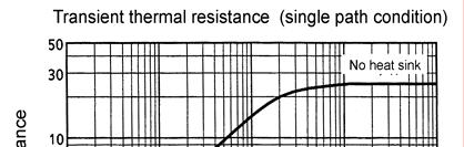
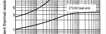
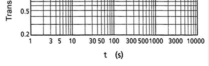
25 25 Power Dissipation TB6560HQ
26 26 1. How to Turn on the Power Turn on V DD. When the voltage has stabilized, turn on V MA/B. In addition, set the Control Input pins to Low when inputting the power. (All the Control Input pins are pulled down internally.) Once the power is on, the CLK signal is received and excitation advances when RESET goes high and excitation is output when ENABLE goes high. If only RESET goes high, excitation won't be output and only the internal counter will advance. Likewise, if only ENABLE goes high, excitation won't advance even if the CLK signal is input and it will remain in the initial state. The following is an example: <Recommended Control Input Sequence> CLK RESET H L ENABLE H L OUT H L Z Output Internal current Output current setting Z Internal current setting: Invariable Output OFF Internal current setting: Variable 2. Calculating the To perform constant-current operations, it is necessary to configure the base current using an external resistor. If the voltage on the N FA (B) pin is 0.5 V (with a torque of 100%) or greater, it will not charge. Ex.: If the maximum current value is 1 A, the external resistance will be 0.5 W. 3. PWM Oscillator Frequency (External Condenser ) An external condenser connected to the OSC pin is used to internally generate a saw tooth waveform. PWM is controlled using this frequency. Toshiba recommends 100 to 3300 pf for the capacitance, taking variations between ICs into consideration. Approximation: f osc = 1/(C osc 1.5 (10/C osc + 1)/66) 1000 khz 4. Power Dissipation The IC power dissipation is determined by the following equation: P = V DD I DD + I OUT Ron 2 drivers The higher the ambient temperature, the smaller the power dissipation. Check the PD-Ta curve, and be sure to design the heat dissipation with a sufficient margin. 5. Heat Sink Fin Processing The IC fin (rear) is electrically connected to the rear of the chip. If current flows to the fin, the IC will malfunction. If there is any possibility of a voltage being generated between the IC GND and the fin, either ground the fin or insulate it.
27 27 6. Thermal Protection When the temperature reaches 170 C (as standard value), the thermal protection circuit is activated switching the output to off. There is a variation of plus or minus about 20 C in the temperature that triggers the circuit operation.
28 28 5 V 10 µf 1 µf 47 µf 1 µf 24 V CLK V DD V MA V MB RESET ENABLE Logic H-SW A OUTAP OUTAM M1 MCU or External input M2 CW/CCW DCY1 DCY2 Control CompA OUTBP H-SW B OUTBM N FA CompB A M TQ1 TQ2 Protect N FB B MO OSC SGND PGND 3.3 V or 5.0 V R1 R2 100 pf 400 khz 0.5 Ω: IOUTmax = 1.0 A
29 29 Package Dimensions Weight: 9.86 g (typ.)
30 30 Package Dimensions Weight: 0.26 g (typ.) Note: The rear heat sink block will be 5.5 mm 5.5 mm. (PROVISIONAL)
31 31 RESTRICTIONS ON PRODUCT USE EBA The information contained herein is subject to change without notice _D TOSHIBA is continually working to improve the quality and reliability of its products. Nevertheless, semiconductor devices in general can malfunction or fail due to their inherent electrical sensitivity and vulnerability to physical stress. It is the responsibility of the buyer, when utilizing TOSHIBA products, to comply with the standards of safety in making a safe design for the entire system, and to avoid situations in which a malfunction or failure of such TOSHIBA products could cause loss of human life, bodily injury or damage to property. In developing your designs, please ensure that TOSHIBA products are used within specified operating ranges as set forth in the most recent TOSHIBA products specifications. Also, please keep in mind the precautions and conditions set forth in the Handling Guide for Semiconductor Devices, or TOSHIBA Semiconductor Reliability Handbook etc _A The TOSHIBA products listed in this document are intended for usage in general electronics applications (computer, personal equipment, office equipment, measuring equipment, industrial robotics, domestic appliances, etc.). These TOSHIBA products are neither intended nor warranted for usage in equipment that requires extraordinarily high quality and/or reliability or a malfunction or failure of which may cause loss of human life or bodily injury ( Unintended Usage ). Unintended Usage include atomic energy control instruments, airplane or spaceship instruments, transportation instruments, traffic signal instruments, combustion control instruments, medical instruments, all types of safety devices, etc. Unintended Usage of TOSHIBA products listed in this document shall be made at the customer s own risk _B The products described in this document shall not be used or embedded to any downstream products of which manufacture, use and/or sale are prohibited under any applicable laws and regulations _Q The information contained herein is presented only as a guide for the applications of our products. No responsibility is assumed by TOSHIBA for any infringements of patents or other rights of the third parties which may result from its use. No license is granted by implication or otherwise under any patent or patent rights of TOSHIBA or others _C The products described in this document are subject to the foreign exchange and foreign trade laws _E
TB6560AHQ, TB6560AFG
 TOSHIBA BiCD Integrated Circuit Silicon Monolithic TB6560AHQ, TB6560AFG PWM Chopper-Type Bipolar Driver IC for Stepping Motor Control TB6560AHQ/AFG The TB6560AHQ/AFG is a PWM chopper-type stepping motor
TOSHIBA BiCD Integrated Circuit Silicon Monolithic TB6560AFTG
 TOSHIBA BiCD Integrated Circuit Silicon Monolithic PWM Chopper-Type Bipolar Driver IC for Stepping Motor Control The is a PWM chopper-type stepping motor driver IC designed for sinusoidal-input microstep
TOSHIBA BiCD Processor IC Silicon Monolithic TB62206F/FG
 TOSHIBA BiCD Processor IC Silicon Monolithic TB62206F/FG BiCD PWM 2 Phase Bipolar Stepping Motor Driver The TB62206F/FG is designed to drive a 2 phase bipolar setpping motor. With BiCD process technology,
THB6064AH. PWM Chopper-Type bipolar Stepping Motor Driver IC. Features
 PWM Chopper-Type bipolar Stepping Motor Driver IC The is a PWM chopper-type sinusoidal micro-step bipolar stepping motor driver IC. It supports 8 kind of excitation modes and forward/reverse mode and is
TOSHIBA BiCD Digital Integrated Circuit Silicon Monolithic TB62752AFUG GND
 TOSHIBA BiCD Digital Integrated Circuit Silicon Monolithic Step Up Type DC/DC Converter for White LED Features The is a high efficient Step-Up Type DC/DC Converter specially designed for constant current
TOSHIBA Bipolar Linear Integrated Circuit Silicon Monolithic TA8050FG
 TOSHIBA Bipolar Linear Integrated Circuit Silicon Monolithic TA8050FG 1.5-A DC Motor Driver with Brake Function The TA8050FG is a 1.5-A motor driver which directly drives a bidirectional DC motor. Inputs
TB6560AHQ Usage Considerations
 TB6560AHQ Usage Considerations The TB6560AHQ drives a two-phase bipolar stepping motor. It drives at a constant current by PWM control. The TB6560AHQ can be used in applications that require 2-phase, 1-2-phase,
TA8435H/HQ TA8435H/HQ PWM CHOPPER-TYPE BIPOLAR STEPPING MOTOR DRIVER. FEATURES TOSHIBA BIPOLAR LINEAR INTEGRATED CIRCUIT SILICON MONOLITHIC
 TOSHIBA BIPOLAR LINEAR INTEGRATED CIRCUIT SILICON MONOLITHIC TA8435H/HQ TA8435H/HQ PWM CHOPPER-TYPE BIPOLAR STEPPING MOTOR DRIVER. The TA8435H/HQ is a PWM chopper-type sinusoidal micro-step bipolar stepping
TC74AC14P,TC74AC14F,TC74AC14FN,TC74AC14FT
 Hex Schmitt Inverter TOSHIBA CMOS Digital Integrated Circuit Silicon Monolithic TC74AC14P/F/FN/FT TC74AC14P,TC74AC14F,TC74AC14FN,TC74AC14FT The TC74AC14 is an advanced high speed CMOS SCHMITT INVERTER
TOSHIBA Bi CMOS INTEGRATED CIRCUIT SILICON MONOLITHIC TB6526AF
 TOSHIBA Bi CMOS INTEGRATED CIRCUIT SILICON MONOLITHIC TB6526AF TB6526AF CHOPPER TYPE BIPOLAR STEPPING MOTOR CONTROL DRIVER IC The TB6526AF is a PWM chopper type sinusoidal micro step bipolar stepping motor
TD62383PG TD62383PG. 8 ch Low Input Active Sink Driver. Features. Pin Assignment (top view) Schematics (each driver)
 Schematics (each driver)") 8 ch Low Input Active Sink Driver TOSHIBA Bipolar Digital Integrated Circuit Silicon Monolithic TD62383PG The TD62383PG is non inverting transistor array which is comprised of eight Low saturation output
8 ch Low Input Active Sink Driver TOSHIBA Bipolar Digital Integrated Circuit Silicon Monolithic TD62383PG The TD62383PG is non inverting transistor array which is comprised of eight Low saturation output
TC74ACT74P,TC74ACT74F,TC74ACT74FN,TC74ACT74FT
 TOSHIBA CMOS Digital Integrated Circuit Silicon Monolithic TC74ACT74P/F/FN/FT TC74ACT74P,TC74ACT74F,TC74ACT74FN,TC74ACT74FT Dual D-Type Flip Flop with Preset and Clear The TC74ACT74 is an advanced high
TC74AC05P,TC74AC05F,TC74AC05FN
 TOSHIBA CMOS Digital Integrated Circuit Silicon Monolithic TC74AC05P/F/FN TC74AC05P,TC74AC05F,TC74AC05FN Hex Inverter (open drain) The TC74AC05 is an advanced high speed CMOS INVERTER fabricated with silicon
TOSHIBA Bipolar Digital Integrated Circuit Silicon Monolithic
 TOSHIBA Bipolar Digital Integrated Circuit Silicon Monolithic TD6251PG,TD6251FG,TD6252PG,TD6252FG,TD6253PG,TD6253FG,TD6254PG TD6254FG,TD6255PG,TD6255FG,TD6256PG,TD6256FG,TD6257PG,TD6257FG 7ch Single Driver,
ULN2003AP,ULN2003AFW,ULN2004AP,ULN2004AFW (Manufactured by Toshiba Malaysia)
") TOSHIBA Bipolar Digital Integrated Circuit Silicon Monolithic ULN2003,04AP/AFW ULN2003AP,ULN2003AFW,ULN2004AP,ULN2004AFW (Manufactured by Toshiba Malaysia) 7ch Darlington Sink Driver The ULN2003AP/AFW
TOSHIBA Bipolar Digital Integrated Circuit Silicon Monolithic ULN2003,04AP/AFW ULN2003AP,ULN2003AFW,ULN2004AP,ULN2004AFW (Manufactured by Toshiba Malaysia) 7ch Darlington Sink Driver The ULN2003AP/AFW
TC74ACT139P,TC74ACT139F,TC74ACT139FN,TC74ACT139FT
 TOSHIBA CMOS Digital Integrated Circuit Silicon Monolithic TC74ACT39P/F/FN/FT TC74ACT39P,TC74ACT39F,TC74ACT39FN,TC74ACT39FT Dual 2-to-4 Line Decoder The TC74ACT39 is an advanced high speed CMOS 2 to 4
TC74AC00P,TC74AC00F,TC74AC00FN,TC74AC00FT
 TOSHIBA CMOS Digital Integrated Circuit Silicon Monolithic TC74AC00P/F/FN/FT TC74AC00P,TC74AC00F,TC74AC00FN,TC74AC00FT Quad 2-Input NAND Gate The TC74AC00 is an advanced high speed CMOS 2-INPUT NAND GATE
TD62318APG,TD62318AFG
 TOSHIBA Bipolar Digital Integrated Circuit Silicon Monolithic TD62318APG,TD62318AFG 4ch Low Input Active High-Current Darlington Sink Driver TD62318APG/AFG The TD62318APG and TD62318AFG are non-inverting
ULN2803APG,ULN2803AFWG,ULN2804APG,ULN2804AFWG (Manufactured by Toshiba Malaysia)
") TOSHIBA Bipolar Digital Integrated Circuit Silicon Monolithic ULN2803,04APG/AFWG ULN2803APG,ULN2803AFWG,ULN2804APG,ULN2804AFWG (Manufactured by Toshiba Malaysia) 8ch Darlington Sink Driver The ULN2803APG
TOSHIBA Bipolar Digital Integrated Circuit Silicon Monolithic ULN2803,04APG/AFWG ULN2803APG,ULN2803AFWG,ULN2804APG,ULN2804AFWG (Manufactured by Toshiba Malaysia) 8ch Darlington Sink Driver The ULN2803APG
TA7291P, TA7291S/SG, TA7291F/FG
 TOSHIBA BIPOLAR LINEAR INTEGRATED CIRCUIT SILICON MONOLITHIC TA7291P, TA7291S/SG, TA7291F/FG BRIDGE DRIVER The TA7291P / S/SG / F/FG are Bridge Driver with output voltage control. FEATURES 4 modes available
TC74AC367P,TC74AC367F,TC74AC367FN,TC74AC367FT
 TOSHIBA CMOS Digital Integrated Circuit Silicon Monolithic TC74AC367P/F/FN/FT TC74AC367P,TC74AC367F,TC74AC367FN,TC74AC367FT Hex Bus Buffer (3-state) The TC74AC367 is an advanced high speed CMOS HEX BUS
TOSHIBA Intelligent Power Device Silicon Monolithic Power MOS Integrated Circuit TPD2005F
 TOSHIBA Intelligent Power Device Silicon Monolithic Power MOS Integrated Circuit TPD2005F TPD2005F ow-side Power Switch Array (8 Channels) for Motors, Solenoids, and amp Drivers The TPD2005F is an 8-channel
ULN2803AP,ULN2803AFW,ULN2804AP,ULN2804AFW (Manufactured by Toshiba Malaysia)
") TOSHIBA BIPOLAR DIGITAL INTEGRATED CIRCUIT SILICON MONOLITHIC ULN2803AP,ULN2803AFW,ULN2804AP,ULN2804AFW (Manufactured by Toshiba Malaysia) 8CH DARLINGTON SINK DRIVER The ULN2803AP / AFW Series are high
TOSHIBA BIPOLAR DIGITAL INTEGRATED CIRCUIT SILICON MONOLITHIC ULN2803AP,ULN2803AFW,ULN2804AP,ULN2804AFW (Manufactured by Toshiba Malaysia) 8CH DARLINGTON SINK DRIVER The ULN2803AP / AFW Series are high
TC4011BP,TC4011BF,TC4011BFN,TC4011BFT
 TOSHIBA CMOS Digital Integrated Circuit Silicon Monolithic TC4011BP/BF/BFN/BFT TC4011BP,TC4011BF,TC4011BFN,TC4011BFT TC4011B Quad 2 Input NAND Gate The TC4011B is 2-input positive logic NAND gate respectively.
TOSHIBA Intelligent Power Device Silicon Monolithic Power MOS Integrated Circuit TPD2007F
 TOSIBA Intelligent Power Device Silicon Monolithic Power MOS Integrated Circuit TPD2007F TPD2007F Low-Side Power Switch Array (8 Channels) for Motors, Solenoids, and Lamp Drivers The TPD2007F is an 8-channel
TC74ACT540P,TC74ACT540F,TC74ACT540FW,TC74ACT540FT TC74ACT541P,TC74ACT541F,TC74ACT541FW,TC74ACT541FT
 TOSHIBA CMOS Digital Integrated Circuit Silicon Monolithic TC74ACT540,541P/F/FW/FT TC74ACT540P,TC74ACT540F,TC74ACT540FW,TC74ACT540FT TC74ACT541P,TC74ACT541F,TC74ACT541FW,TC74ACT541FT Octal Bus Buffer TC74ACT540P/F/FW/FT
TD62783AP,TD62783AF,TD62784AP,TD62784AF
 TOSHIBA Bipolar Digital Integrated Circuit Silicon Monolithic TD62783,784AP/AF TD62783AP,TD62783AF,TD62784AP,TD62784AF 8 ch High-oltage Source Driver The TD62783AP/AF Series are comprised of eight source
TOSHIBA BIPOLAR DIGITAL INTEGRATED CIRCUIT SILICON MONOLITHIC TD62771AP
 TOSHIBA BIPOLAR DIGITAL INTEGRATED CIRCUIT SILICON MONOLITHIC 7CH HIGH VOLTAGE SOURCE DRIVER The is comprised of seven source current Transistor Array. This driver is specifically designed for fluorescent
TD62081AP,TD62081AF,TD62082AP,TD62082AF TD62083AP,TD62083AF,TD62084AP,TD62084AF
 Toshiba Bipolar Digital Integrated Circuit Silicon Monolithic TD6281AP,TD6281AF,TD6282AP,TD6282AF TD6283AP,TD6283AF,TD6284AP,TD6284AF TD6281~84AP/AF 8ch Darlington Sink Driver The TD6281AP/AF Series are
TC74HC540AP,TC74HC540AF,TC74HC540AFW TC74HC541AP,TC74HC541AF,TC74HC541AFW
 TOSHIBA CMOS Digital Integrated Circuit Silicon Monolithic TC74HC540,541AP/AF/AFW TC74HC540AP,TC74HC540AF,TC74HC540AFW TC74HC541AP,TC74HC541AF,TC74HC541AFW Octal Bus Buffer TC74HC540AP/AF/AFW TC74HC541AP/AF/AFW
TC74HC240AP,TC74HC240AF,TC74HC240AFW TC74HC241AP,TC74HC241AF TC74HC244AP,TC74HC244AF,TC74HC244AFW
 TOSHIBA CMOS Digital Integrated Circuit Silicon Monolithic TC74HC240AP,TC74HC240AF,TC74HC240AFW TC74HC241AP,TC74HC241AF TC74HC244AP,TC74HC244AF,TC74HC244AFW Octal Bus Buffer TC74HC240AP/AF/AFW TC74HC241AP/AF
TD62308AP,TD62308AF TD62308AP/AF. 4ch Low Input Active High-Current Darlington Sink Driver. Features. Pin Assignment (top view)
") TOSHIBA Bipolar Digital Integrated Circuit Silicon Monolithic TD6238AP,TD6238AF 4ch Low Input Active High-Current Darlington Sink Driver TD6238AP/AF The TD6238AP/AF is a non inverting transistor array
TOSHIBA Bipolar Digital Integrated Circuit Silicon Monolithic TD6238AP,TD6238AF 4ch Low Input Active High-Current Darlington Sink Driver TD6238AP/AF The TD6238AP/AF is a non inverting transistor array
TC74VHC14F,TC74VHC14FN,TC74VHC14FT,TC74VHC14FK
 TOSHIBA CMOS Digital Integrated Circuit Silicon Monolithic TC74VHC14F/FN/FT/FK TC74VHC14F,TC74VHC14FN,TC74VHC14FT,TC74VHC14FK Hex Schmitt Inverter The TC74VHC14 is an advanced high speed CMOS SCHMITT INVERTER
TC74HC4066AP,TC74HC4066AF,TC74HC4066AFN,TC74HC4066AFT
 TOSHIBA CMOS Digital Integrated Circuit Silicon Monolithic TC74HC4066AP/AF/AFN/AFT TC74HC4066AP,TC74HC4066AF,TC74HC4066AFN,TC74HC4066AFT Quad Bilateral Switch The TC74HC4066A is a high speed CMOS QUAD
TC74VHC32F,TC74VHC32FN,TC74VHC32FT,TC74VHC32FK
 TOSHIBA CMOS Digital Integrated Circuit Silicon Monolithic TC74VHC32F/FN/FT/FK TC74VHC32F,TC74VHC32FN,TC74VHC32FT,TC74VHC32FK Quad 2-Input OR Gate The TC74VHC32 is an advanced high speed CMOS 2-INPUT OR
TOSHIBA CMOS Digital Integrated Circuit Silicon Monolithic TC4521BP
 TOSHIBA CMOS Digital Integrated Circuit Silicon Monolithic 24-Stage Frequency Divider is frequency divider coisting of 24 stages of flip-flop. The input section is equipped with an inverter to enable to
TOSHIBA BiCD Digital Integrated Circuit Silicon Monolithic TB62756FUG
 TOSHIBA BiCD Digital Integrated Circuit Silicon Monolithic Step-up Type DC/DC Converter for White LEDs The is a high efficiency step-up type DC/DC converter that is designed especially for use as a constant
TD62786AP,TD62786AF,TD62787AP,TD62787AF
 TOSHIBA BIPOLAR DIGITAL INTEGRATED CIRCUIT SILICON MONOLITHIC TD62786AP,TD62786AF,TD62787AP,TD62787AF 8CH HIGH VOLTAGE SOURCE DRIVER The TD62786AP / AF series are eight channel huyx non inverting source
GT30J322 GT30J322 FOURTH-GENERATION IGBT CURRENT RESONANCE INVERTER SWITCHING APPLICATIONS. MAXIMUM RATINGS (Ta = 25 C) EQUIVALENT CIRCUIT MARKING
 EQUIVALENT CIRCUIT MARKING") TOSHIBA INSULATED GATE BIPOLAR TRANSISTOR SILICON N CHANNEL IGBT FOURTH-GENERATION IGBT CURRENT RESONANCE INVERTER SWITCHING APPLICATIONS Unit: mm FRD included between emitter and collector Enhancement
TOSHIBA INSULATED GATE BIPOLAR TRANSISTOR SILICON N CHANNEL IGBT FOURTH-GENERATION IGBT CURRENT RESONANCE INVERTER SWITCHING APPLICATIONS Unit: mm FRD included between emitter and collector Enhancement
TLP557 TLP557. Transistor Invertor Inverter For Air Conditionor Power Transistor Base Drive. Pin Configuration (top view) Schmatic.
 Schmatic.") TOSHIB Photocoupler Gals Ired & Photo IC Transistor Invertor Inverter For ir Conditionor Power Transistor Base Drive Unit in mm The TOSHIB consists of a Gals light emitting diode and a integrated photodetector.
TOSHIB Photocoupler Gals Ired & Photo IC Transistor Invertor Inverter For ir Conditionor Power Transistor Base Drive Unit in mm The TOSHIB consists of a Gals light emitting diode and a integrated photodetector.
ULN2803AP,ULN2803AFW,ULN2804AP,ULN2804AFW (Manufactured by Toshiba Malaysia)
") TOSHIBA BIPOLAR DIGITAL INTEGRATED CIRCUIT SILICON MONOLITHIC ULN2803AP,ULN2803AFW,ULN2804AP,ULN2804AFW (Manufactured by Toshiba Malaysia) 8CH DARLINGTON SINK DRIVER The ULN2803AP / AFW Series are high
TOSHIBA BIPOLAR DIGITAL INTEGRATED CIRCUIT SILICON MONOLITHIC ULN2803AP,ULN2803AFW,ULN2804AP,ULN2804AFW (Manufactured by Toshiba Malaysia) 8CH DARLINGTON SINK DRIVER The ULN2803AP / AFW Series are high
TOSHIBA BIPOLAR DIGITAL INTEGRATED CIRCUIT SILICON MONOLITHIC
 TOSHIBA BIPOLAR DIGITAL INTEGRATED CIRCUIT SILICON MONOLITHIC TD62001P,TD62001AP,TD62001F,TD62001AF,TD62002P TD62002AP,TD62002F,TD62002AF,TD62003P,TD62003AP,TD62003F TD62003AF,TD62004P,TD62004AP,TD62004F,TD62004AF
TC74LCX07F,TC74LCX07FN,TC74LCX07FT,TC74LCX07FK
 TOSHIBA CMOS Digital Integrated Circuit Silicon Monolithic TC74LCX07F/FN/FT/FK TC74LCX07F,TC74LCX07FN,TC74LCX07FT,TC74LCX07FK Low-Voltage HEX Buffer with 5-V Tolerant Inputs and Outputs (open drain) The
GT50J301 GT50J301 HIGH POWER SWITCHING APPLICATIONS MOTOR CONTROL APPLICATIONS. MAXIMUM RATINGS (Ta = 25 C) EQUIVALENT CIRCUIT
 EQUIVALENT CIRCUIT") TOSHIBA INSULATED GATE BIPOLAR TRANSISTOR SILICON N CHANNEL IGBT GT50J301 GT50J301 HIGH POWER SWITCHING APPLICATIONS MOTOR CONTROL APPLICATIONS Unit: mm Third generation IGBT Enhancement mode type High
TOSHIBA INSULATED GATE BIPOLAR TRANSISTOR SILICON N CHANNEL IGBT GT50J301 GT50J301 HIGH POWER SWITCHING APPLICATIONS MOTOR CONTROL APPLICATIONS Unit: mm Third generation IGBT Enhancement mode type High
TOSHIBA Bi CD Integrated Circuit Silicon Monolithic TB6608FNG
 TOSHIBA Bi CD Integrated Circuit Silicon Monolithic Stepping Motor Driver IC The is a PWM constant-current type stepping motor driver IC designed for sinusoidal-input micro-step control of stepping motors.
TA7736P,TA7736F TA7736P/F DC MOTOR DRIVER IC FEATURES TOSHIBA BIPOLAR LINEAR INTEGRATED CIRCUIT SILICON MONOLITHIC
 TOSHIBA BIPOLAR LINEAR INTEGRATED CIRCUIT SILICON MONOLITHIC TA7736P,TA7736F TA7736P/F DC MOTOR DRIVER IC The TA7736P is a 3 phase Bi directional motor driver IC. It designed for use VCR, tape deck, floppy
TA8210AHQ,TA8210ALQ Features
 TOSHIBA Bipolar Linear Integrated Circuit Silicon Monolithic TA8210AHQ,TA8210ALQ TA8210AHQ/ALQ 20W BTL 2ch Audio Power Amplifier The thermal resistance θj T of TA8210AHQ, TA8210ALQ package designed for
TC7WH04FU,TC7WH04FK TC7WH04FU/FK. Triple Inverter. Features. Marking. Pin Assignment (top view)
") TOSHIBA CMOS Digital Integrated Circuit Silicon Monolithic TC7WH04FU,TC7WH04FK TC7WH04FU/FK Triple Inverter The TC7WH04 is an advanced high speed CMOS Inverter fabricated with silicon gate CMOS technology.
TOSHIBA CMOS Digital Integrated Circuit Silicon Monolithic TC7WH04FU,TC7WH04FK TC7WH04FU/FK Triple Inverter The TC7WH04 is an advanced high speed CMOS Inverter fabricated with silicon gate CMOS technology.
TOSHIBA Field Effect Transistor Silicon N Channel MOS Type (π MOSV) 2SK3265
 2SK3265") TOSHIBA Field Effect Transistor Silicon N Channel MOS Type (π MOSV) 2SK3265 Chopper Regulators DC DC Converter and Motor Drive Applications Unit: mm Low drain source ON resistance : RDS (ON) = 0.72 Ω (typ.)
TOSHIBA Field Effect Transistor Silicon N Channel MOS Type (π MOSV) 2SK3265 Chopper Regulators DC DC Converter and Motor Drive Applications Unit: mm Low drain source ON resistance : RDS (ON) = 0.72 Ω (typ.)
查询 D2553 供应商 2SD2553 TOSHIBA TRANSISTOR SILICON NPN TRIPLE DIFFUSED MESA TYPE 2SD2553. DC I C 8 A Pulse I CP 16
 查询 D2553 供应商 2SD2553 TOSHIBA TRANSISTOR SILICON NPN TRIPLE DIFFUSED MESA TYPE 2SD2553 HORIZONTAL DEFLECTION OUTPUT FOR HIGH RESOLUTION DISPLAY, COLOR TV HIGH SPEED SWITCHING APPLICATIONS Unit: mm High
TOSHIBA INSULATED GATE BIPOLAR TRANSISTOR SILICON N CHANNEL IGBT GT50J301
 TOSHIBA INSULATED GATE BIPOLAR TRANSISTOR SILICON N CHANNEL IGBT GT50J301 GT50J301 HIGH POWER SWITCHING APPLICATIONS MOTOR CONTROL APPLICATIONS Unit: mm Third generation IGBT Enhancement mode type High
TB62747AFG,TB62747AFNG, TB62747AFNAG,TB62747BFNAG
 TOSHIB Bi-CMOS Integrated Circuit Silicon Monolithic TB62747FG,TB62747FNG, TB62747FNG,TB62747BFNG 16-Output Constant Current LED Driver The TB62747 series is comprised of constant-current drivers designed
TOSHIBA INSULATED GATE BIPOLAR TRANSISTOR SILICON N CHANNEL IGBT GT30J322
 TOSHIBA INSULATED GATE BIPOLAR TRANSISTOR SILICON N CHANNEL IGBT GT30J322 GT30J322 FOURTH-GENERATION IGBT CURRENT RESONANCE INVERTER SWITCHING APPLICATIONS Unit: mm FRD included between emitter and collector
TB62726ANG,TB62726AFG
 TOSHIBA Bi-CMOS Integrated Circuit Silicon Monolithic TB62726ANG,TB62726AFG 16-bit Constant-Current LED Driver with Operating Voltage of 3.3-V and 5-V The TB62726A series are comprised of constant-current
TOSHIBA CMOS Integrated Circuit Silicon Monolithic TB6575FNG
 TOSHIBA CMOS Integrated Circuit Silicon Monolithic TB6575FNG PWM Sensorless Controller for 3-Phase Full-Wave BLDC Motors The TB6575FNG provides sensorless commutation and PWM current control for 3-phase
TC4584BP,TC4584BF,TC4584BFN
 TC484BP/BF/BFN TOSHIBA CMOS Digital Integrated Circuit Silicon Monolithic TC484BP,TC484BF,TC484BFN TC484B Hex Schmitt Trigger The TC484B is the 6-circuit inverter having the Schmitt trigger function at
TOSHIBA Transistor Silicon PNP Epitaxial Type 2SA1930
 TOSHIBA Transistor Silicon PNP Epitaxial Type 2SA193 Power Amplifier Applications Driver Stage Amplifier Applications Unit: mm High transition frequency: f T = 2 MHz (typ.) Complementary to 2SC5171 Absolute
TOSHIBA Field Effect Transistor Silicon P Channel MOS Type 2SJ200
 TOSHIBA Field Effect Transistor Silicon P Channel MOS Type 2SJ200 High Power Amplifier Application Unit: mm High breakdown voltage High forward transfer admittance Complementary to 2SK1529 : V DSS = 180
TOSHIBA Field Effect Transistor Silicon N Channel MOS Type (π MOSII.5 ) 2SK1120. DC (Note 1) I D 8 A Pulse (Note 1) I DP 24
 2SK1120. DC (Note 1) I D 8 A Pulse (Note 1) I DP 24") TOSHIBA Field Effect Transistor Silicon N Channel MOS Type (π MOSII.5 ) 2SK1120 2SK1120 DC DC Converter and Motor Drive Applications Unit: mm Low drain source ON resistance : RDS (ON) = 1.5 Ω (typ.) High
TOSHIBA Field Effect Transistor Silicon N Channel MOS Type (π MOSII.5 ) 2SK1120 2SK1120 DC DC Converter and Motor Drive Applications Unit: mm Low drain source ON resistance : RDS (ON) = 1.5 Ω (typ.) High
2SD1508 2SD1508. Pulse Motor Drive, Hammer Drive Applications Switching Applications Power Amplifier Applications. Maximum Ratings (Ta = 25 C)
") TOSHIBA Transistor Silicon NPN Epitaxial Type (PCT process) (Darlington power transistor) Pulse Motor Drive, Hammer Drive Applications Switching Applications Power Amplifier Applications Unit: mm High
TOSHIBA Transistor Silicon NPN Epitaxial Type (PCT process) (Darlington power transistor) Pulse Motor Drive, Hammer Drive Applications Switching Applications Power Amplifier Applications Unit: mm High
TC4538BP,TC4538BF TC4538BP/BF. TC4538BP/TC4538BF Dual Precision Retriggerable/Resettable Monostable Multivibrator. Features.
 TC438BP/BF TOSHIBA CMOS Digital Integrated Circuit Silicon Monolithic TC438BP,TC438BF TC438BP/TC438BF Dual Precision Retriggerable/Resettable Monostable Multivibrator The TC438BP/BF is the retriggerable/resettable
TA8227P TA8227P. Low Frequency Power Amplifier. Features TOSHIBA Bipolar Linear Integrated Circuit Silicon Monolithic
 TOSHIBA Bipolar Linear Integrated Circuit Silicon Monolithic TA8227P Low Frequency Power Amplifier TA8227P is an audio power IC with built-in two channels developed for portable radio cassette tape recorder
TOSHIBA Field Effect Transistor Silicon P-Channel MOS Type (U MOS III) 2SJ669
 2SJ669") TOSHIBA Field Effect Transistor Silicon P-Channel MOS Type (U MOS III) Relay Drive, DC/DC Converter and Motor Drive Applications Unit: mm 4-V gate drive Low drain-source ON-resistance: R DS (ON) =.2 Ω
TOSHIBA Field Effect Transistor Silicon P-Channel MOS Type (U MOS III) Relay Drive, DC/DC Converter and Motor Drive Applications Unit: mm 4-V gate drive Low drain-source ON-resistance: R DS (ON) =.2 Ω
TC74HC423AP,TC74HC423AF
 TOSHIBA CMOS Digital Integrated Circuit Silicon Monolithic TC74HC423AP,TC74HC423AF Dual Retriggerable Monostable Multivibrator The TC74HC423A is a high speed CMOS MONOSTABLE MULTIVIBRATOR fabricated with
TOSHIBA BiCD Digital Integrated Circuit Silicon Monolithic TB62736FUG
 TOSHIBA BiCD Digital Integrated Circuit Silicon Monolithic TB62736FUG Step-up Type DC/DC Converter for White LEDs The TB62736FUG is a high efficiency step-up type DC/DC converter that is designed especially
TA2111NG,TA2111FG,TA2111FNG
 TOSHIBA Bipolar Linear Integrated Circuit Silicon Monolithic TA2111NG,TA2111FG,TA2111FNG 3 V AM/FM 1 Chip Tuner IC TA2111NG/FG/FNG are AM/FM 1 chip tuner ICs, which are designed for portable radios and
TC74HC123AP,TC74HC123AF,TC74HC123AFN
 TOSHIBA CMOS Digital Integrated Circuit Silicon Monolithic TC74HC123AP/AF/AFN TC74HC123AP,TC74HC123AF,TC74HC123AFN Dual Retriggerable Monostable Multivibrator The TC74HC123A is a high speed CMOS MONOSTABLE
2SA2066 2SA2066. High-Speed Switching Applications DC-DC Converter Applications. Maximum Ratings (Ta = 25 C) Electrical Characteristics (Ta = 25 C)
 Electrical Characteristics (Ta = 25 C)") TOSHIBA Transistor Silicon PNP Epitaxial Type 2SA266 High-Speed Switching Applications DC-DC Converter Applications Unit: mm High DC current gain: hfe = 2 to 5 (IC =.2 A) Low collector-emitter saturation
TOSHIBA Transistor Silicon PNP Epitaxial Type 2SA266 High-Speed Switching Applications DC-DC Converter Applications Unit: mm High DC current gain: hfe = 2 to 5 (IC =.2 A) Low collector-emitter saturation
TOSHIBA Transistor Silicon PNP Epitaxial Type TPC
 TOSHIBA Transistor Silicon PNP Epitaxial Type TPC662 High-Speed Switching Applications DC-DC Converter Applications Strobe Applications Unit: mm High DC current gain: h FE = 2 to 5 (I C =.2 A) Low collector-emitter
TB6559FG TB6559FG. Full-Bridge DC Motor Driver IC. Features TOSHIBA Bi-CD Integrated Circuit Silicon Monolithic
 TOSHIBA Bi-CD Integrated Circuit Silicon Monolithic Full-Bridge DC Motor Driver IC The is a full-bridge DC motor driver with DMOS output transistors. It uses P-channel MOSFETs on the high side and N-channel
TCA62724FMG TCA62724FMG. 3-Channel Constant-Current LED Driver. Features TOSHIBA CMOS Integrated Circuits Silicon Monolithic
 TOSHIBA CMOS Integrated Circuits Silicon Monolithic TCA62724FMG 3-Channel Constant-Current LED Driver The TCA62724FM is an optimal constant-current LED driver for RGB pixel LEDs. The device supports 16
TA8223K TA8223K. Low Frequency Power Amplifier. Features TOSHIBA Bipolar Linear Integrated Circuit Silicon Monolithic
 TOSHIBA Bipolar Linear Integrated Circuit Silicon Monolithic TA8223K Low Frequency Power Amplifier TA8223K is an audio power IC with built-in two channels developed for portable radio cassette tape recorder
TOSHIBA Transistor Silicon NPN Epitaxial Type (PCT process) (Darlington power transistor) 2SD1508
 (Darlington power transistor) 2SD1508") 2SD8 TOSHIBA Transistor Silicon NPN Epitaxial Type (PCT process) (Darlington power transistor) 2SD8 Pulse Motor Drive, Hammer Drive Applications Switching Applications Power Amplifier Applications Unit:
2SD8 TOSHIBA Transistor Silicon NPN Epitaxial Type (PCT process) (Darlington power transistor) 2SD8 Pulse Motor Drive, Hammer Drive Applications Switching Applications Power Amplifier Applications Unit:
TOSHIBA Insulated Gate Bipolar Transistor Silicon N Channel IGBT GT45F123
 GT45F3 TOSHIBA Insulated Gate Bipolar Transistor Silicon N Channel IGBT GT45F3 For PDP-TV Applications Unit: mm 5th generation (trench gate structure) IGBT Enhancement-mode Low input capacitance: Cies
2SD2638 2SD2638. Horizontal Deflection Output for Color TV, Digital TV High Speed Switching Applications. Maximum Ratings (Tc = 25 C)
") SD TOSHIBA Transistor Silicon NPN Triple Diffused Mesa Type SD Horizontal Deflection Output for Color TV, Digital TV High Speed Switching Applications Unit: mm High voltage: VCBO = 7 V Low saturation voltage:
SD TOSHIBA Transistor Silicon NPN Triple Diffused Mesa Type SD Horizontal Deflection Output for Color TV, Digital TV High Speed Switching Applications Unit: mm High voltage: VCBO = 7 V Low saturation voltage:
TOSHIBA Transistor Silicon NPN Epitaxial Type 2SC5886
 TOSHIBA Transistor Silicon NPN Epitaxial Type SC886 High-Speed Swtching Applications DC-DC Converter Applications Unit: mm High DC current gain: h FE = 4 to (I C =. A) Low collector-emitter saturation:
TOSHIBA Transistor Silicon NPN Epitaxial Type (Darlington Power) 2SD
 2SD") TOSHIBA Transistor Silicon NPN Epitaxial Type (Darlington Power) 2SD2686 Solenoid Drive Applications Motor Drive Applications Unit: mm High DC current gain: h FE = 2 (min) (V CE = 2 A, I C = A) Zener diode
TOSHIBA Transistor Silicon NPN Epitaxial Type (Darlington Power) 2SD2686 Solenoid Drive Applications Motor Drive Applications Unit: mm High DC current gain: h FE = 2 (min) (V CE = 2 A, I C = A) Zener diode
TOSHIBA TRANSISTOR SILICON NPN TRIPLE DIFFUSED MESA TYPE 2SC5612
 TOSHIBA TRANSISTOR SILICON NPN TRIPLE DIFFUSED MESA TYPE 2SC5612 2SC5612 HORIZONTAL DEFLECTION OUTPUT FOR COLOR TV Unit: mm High Voltage Low Saturation Voltage High Speed : V CBO = 2000 V : V CE (sat)
TOSHIBA Field Effect Transistor Silicon N Channel MOS Type (π MOSV) 2SK2750
 2SK2750") TOSHIBA Field Effect Transistor Silicon N Channel MOS Type (π MOSV) 2SK2750 Chopper Regulator, DC DC Converter and Motor Drive Applications Unit: mm Low drain source ON resistance : RDS (ON) = 1.7 Ω (typ.)
TOSHIBA Field Effect Transistor Silicon N Channel MOS Type (π MOSV) 2SK2750 Chopper Regulator, DC DC Converter and Motor Drive Applications Unit: mm Low drain source ON resistance : RDS (ON) = 1.7 Ω (typ.)
2SC2873 2SC2873. Power Amplifier Applications Power Switching Applications. Maximum Ratings (Ta = 25 C)
") TOSHIBA Transistor Silicon NPN Epitaxial Type (PCT Process) 2SC2873 Power Amplifier Applications Power Switching Applications Unit: mm Low saturation voltage: VCE (sat) =. V (max) (IC = A) High-speed switching
TOSHIBA Transistor Silicon NPN Epitaxial Type (PCT Process) 2SC2873 Power Amplifier Applications Power Switching Applications Unit: mm Low saturation voltage: VCE (sat) =. V (max) (IC = A) High-speed switching
TOSHIBA Bipolar Linear Integrated Circuit Silicon Monolithic TA8050F
 TOSHIBA Bipolar Linear Integrated Circuit Silicon Monolithic TA050F 1.5 A DC Motor Driver with Brake Function The TA050F is a 1.5 A motor driver which directly drives a bidirectional DC motor. Inputs DI1
TC74HC374AP,TC74HC374AF,TC74HC374AFW
 TOSHIBA CMOS Digital Integrated Circuit Silicon Monolithic TC74HC374AP/AF/AFW TC74HC374AP,TC74HC374AF,TC74HC374AFW Octal D-Type Flip-Flop with 3-State Output The TC74HC374A is a high speed CMOS OCTAL FLIP-FLOP
TC74HC273AP,TC74HC273AF,TC74HC273AFW
 TOSHIBA CMOS Digital Integrated Circuit Silicon Monolithic TC74HC273AP/AF/AFW TC74HC273AP,TC74HC273AF,TC74HC273AFW Octal D-Type Flip Flop with Clear The TC74HC273A is a high speed CMOS OCTAL D-TYPE FLIP
2SC3657 2SC3657. Switching Regulator and High-Voltage Switching Applications High-Speed DC-DC Converter Applications. Maximum Ratings (Tc = 25 C)
") SC67 TOSHIBA Transistor Silicon NPN Triple Diffused Type SC67 Switching Regulator and High-Voltage Switching Applications High-Speed DC-DC Converter Applications Unit: mm Excellent switching times: tr
SC67 TOSHIBA Transistor Silicon NPN Triple Diffused Type SC67 Switching Regulator and High-Voltage Switching Applications High-Speed DC-DC Converter Applications Unit: mm Excellent switching times: tr
TA2149BNG,TA2149BFNG
 TOSHIBA Bipolar Linear Integrated Circuit Silicon Monolithic TA249BNG,TA249BFNG TA249BNG/BFNG V / Chip Tuner IC (for Digital Tuning System) TA249BNG, TA249BFNG are / chip tuner ICs, which are designed
TOSHIBA Insulated Gate Bipolar Transistor Silicon N Channel IGBT GT30J324
 GTJ2 TOSHIBA Insulated Gate Bipolar Transistor Silicon N Channel IGBT GTJ2 High Power Switching Applications Fast Switching Applications Unit: mm Fourth-generation IGBT Enhancement mode type Fast switching
TA8205AHQ,TA8205ALQ Features
 TOSHIBA Bipolar Linear Integrated Circuit Silicon Monolithic TA8205AHQ,TA8205ALQ TA8205AHQ/ALQ 18W BTL 2CH Audio Power Amplifier The thermal resistance θj T of TA8205AHQ, TA8205ALQ package designed for
TOSHIBA Bipolar Linear Integrated Circuit Silicon Monolithic TA8251AH
 TOSHIBA Bipolar Linear Integrated Circuit Silicon Monolithic TA8251AH Max Power 30W BTL 4ch Audio Power IC The TA8251AH is 4ch BTL audio power amplifier for consumer application. It is designed low distortion
TOSHIBA Multi-Chip Transistor Silicon NPN & PNP Epitaxial Type TPC6901. Rating Unit C/W
 TPC69 TOSHIBA Multi-Chip Transistor Silicon NPN & PNP Epitaxial Type TPC69 High-Speed Switching Applications MOS Gate Drive Applications Unit: mm NPN and PNP transistors are mounted on a compact and slim
GT60M323 GT60M323. Voltage Resonance Inverter Switching Application Unit: mm. Maximum Ratings (Ta = 25 C) Thermal Characteristics. Equivalent Circuit
 Thermal Characteristics. Equivalent Circuit") GTM323 TOSHIBA Insulated Gate Bipolar Transistor Silicon N Channel IGBT GTM323 Voltage Resonance Inverter Switching Application Unit: mm Enhancement-mode High speed : tf =.9 µs (typ.) (IC = A) Low saturation
GTM323 TOSHIBA Insulated Gate Bipolar Transistor Silicon N Channel IGBT GTM323 Voltage Resonance Inverter Switching Application Unit: mm Enhancement-mode High speed : tf =.9 µs (typ.) (IC = A) Low saturation
TC74HC175AP,TC74HC175AF,TC74HC175AFN
 TOSHIBA CMOS Digital Integrated Circuit Silicon Monolithic TC74HC175AP/AF/AFN TC74HC175AP,TC74HC175AF,TC74HC175AFN Quad D-Type Flip Flop with Clear The TC74HC175A is a high speed CMOS D-TYPE FLIP FLOP
2SJ401 2SJ401. DC DC Converter, Relay Drive and Motor Drive Applications. Maximum Ratings (Ta = 25 C) Thermal Characteristics
 Thermal Characteristics") TOSHIBA Field Effect Transistor Silicon P Channel MOS Type (L 2 π MOSV) 2SJ401 DC DC Converter, Relay Drive and Motor Drive Applications Unit: mm 4 V gate drive Low drain source ON resistance : RDS (ON)
TOSHIBA Field Effect Transistor Silicon P Channel MOS Type (L 2 π MOSV) 2SJ401 DC DC Converter, Relay Drive and Motor Drive Applications Unit: mm 4 V gate drive Low drain source ON resistance : RDS (ON)
TOSHIBA Transistor Silicon NPN Epitaxial Type (PCT Process) 2SC3423
 2SC3423") TOSHIBA Transistor Silicon NPN Epitaxial Type (PCT Process) SC Audio Frequency Amplifier Applications Unit: mm Complementary to SA6 Small collector output capacitance: C ob =.8 pf (typ.) High transition
TOSHIBA Transistor Silicon NPN Epitaxial Type (PCT Process) SC Audio Frequency Amplifier Applications Unit: mm Complementary to SA6 Small collector output capacitance: C ob =.8 pf (typ.) High transition
2SC5353 2SC5353. Switching Regulator and High Voltage Switching Applications High-Speed DC-DC Converter Applications. Maximum Ratings (Tc = 25 C)
") TOSHIBA Transistor Silicon NPN Triple Diffused Type (PCT process) SC55 Switching Regulator and High Voltage Switching Applications High-Speed DC-DC Converter Applications Unit: mm Excellent switching times:
TOSHIBA Transistor Silicon NPN Triple Diffused Type (PCT process) SC55 Switching Regulator and High Voltage Switching Applications High-Speed DC-DC Converter Applications Unit: mm Excellent switching times:
TB6537P/PG,TB6537F/FG
 TOSHIBA CMOS Integrated Circuit Silicon Monolithic TB6537P/PG,TB6537F/FG TB6537P/PG/F/FG 3-PHASE FULL-WAVE SENSORLESS CONTROLLER FOR BRUSHLESS DC MOTORS The TB6537P/PG/F/FG is a 3-phase full-wave sensorless
TOSHIBA BIPOLAR LINEAR INTEGRATED CIRCUIT SILICON MONOLITHIC TA8429H
 TOSHIBA BIPOLAR LINEAR INTEGRATED CIRCUIT SILICON MONOLITHIC TA8429H TA8429H 3.0A FULL BRIDGE DRIVER The TA8429H is full bridge driver IC for brush motor rotation control that has current capability of
TOSHIBA TRANSISTOR SILICON NPN TRIPLE DIFFUSED MESA TYPE 2SC5858
 SC55 TOSHIBA TRANSISTOR SILICON NPN TRIPLE DIFFUSED MESA TYPE SC55 HORIZONTAL DEFLECTION OUTPUT FOR HDTV, DIGITAL TV, PROJECTION TV Unit: mm High Voltage Low Saturation Voltage High Speed : V CBO = 7 V
TOSHIBA BiCD Processor IC Silicon Monolithic TB62209FG
 TOSHIBA BiCD Processor IC Silicon Monolithic TB62209FG Stepping Motor Driver IC Using PWM Chopper Type The TB62209FG is a stepping motor driver driven by chopper micro-step pseudo sine wave. The TB62209FG
GT8G133 GT8G133. Strobe Flash Applications. Absolute Maximum Ratings (Ta = 25 C) Circuit Configuration. Thermal Characteristics.
 Circuit Configuration. Thermal Characteristics.") TOSHIBA Insulated Gate Bipolar Transistor Silicon N Channel IGBT GT8G Strobe Flash Applications Unit: mm Compact and Thin (TSSOP-8) package Enhancement-mode 4-V gate drive voltage: V GE = 4. V (min) (@I
TOSHIBA Insulated Gate Bipolar Transistor Silicon N Channel IGBT GT8G Strobe Flash Applications Unit: mm Compact and Thin (TSSOP-8) package Enhancement-mode 4-V gate drive voltage: V GE = 4. V (min) (@I
TOSHIBA Transistor Silicon NPN Triple Diffused Type 2SD2406. JEDEC Storage temperature range T stg 55 to 150 C
 TOSHIBA Transistor Silicon NPN Triple Diffused Type Power Amplifier Applications Unit: mm High power dissipation: P C = W () Good h FE linearity Absolute Maximum Ratings () Characteristics Symbol Rating