Antenna Bandwidth and Radiation Control by Topology and use of Non-Conductive Materials
|
|
|
- Isabella Melton
- 5 years ago
- Views:
Transcription
1 Antenna Bandwidth and Radiation Control by Topology and use of Non-Conductive Materials by Hatim A. Bukhari A dissertation submitted in partial fulfillment of the requirements for the degree of Doctor of Philosophy (Electrical Engineering) in The University of Michigan 2016 Doctoral Committee: Professor Kamal Sarabandi, Chair Associate Professor Anthony Grbic Professor Jerome Lynch Professor Eric Michielssen
2 Hatim A. Bukhari 2016 All Rights Reserved
3 DEDICATION To God, then to my mother and father with love and gratitude. ii
4 ACKNOWLEDGMENT First, I would like first to thank God for giving me the power to pursue my dreams and his guidance. I could never have accomplished my Ph.D. without the faith I have in you, the Almighty. I would also like to thank my parents, brother, and sisters for all their love and support throughout the years that I have been away from them, but especially my mother. She was my motivation to pursue my Ph.D. I have had the privilege of having Professor Kamal Sarabandi as my research advisor and dissertation committee chair. Kamal, I want to thank you for your unlimited support, guidance, patience and mentorship in both research and personal life. Your dedication and passion about research has truly inspired me. Additionally, I would like to thank my other committee members, Dr. Anthony Grbic, Dr. Eric Michielssen, and Dr. Jerome Lynch for their guidance and support towards the completion of my Ph.D. work. I would like to express my gratitude and appreciation to many amazing teachers and mentors I have had at the University of Michigan and King Abulaziz City for Science and Technology (KACST). I would like to thank in particular Dr. Sami Alhumaidi, my former boss at KACST, for believing in me and supporting me throughout the years I was there and also towards my Ph.D. here at the University of Michigan. I would like to thank all my friends and colleagues. Adel Elsherbini, thank you for your help and sharing your knowledge with me. Mani Kashanianfard and Xiuzhang Cai, I am thankful for your help in the lab when I needed it. Brian Tierney and Gurkan Gok, I would like to thank you iii
5 both for helping me in fabricating several of my antennas in your lab. Dr. Adib Nashashibi, I am thankful for your advice and assistance on any aspect related to measurements in the lab. Dr. Waleed Alomar and Amr Ibrahim, I would like to thank you both for your support, sharing your knowledge and being my office mates throughout the years. Michael Benson, I am thankful for your effort in reviewing my English grammar in some of my papers. I had the opportunity to interact with many people within the university and outside the school. I have met many outstanding researchers, students and intelligent people during my Ph.D. period. I would like to thank all my colleagues, research groups, office mates, and all my friends. I would have never reached this stage without your support and encouragement. Thank you all for all the good times we have had. Hatim Bukhari November 23, 2015 iv
6 Table of Contents DEDICATION... ii ACKNOWLEDGMENT... iii LIST OF FIGURES... viii ABSTRACT... xiv Chapter 1: Introduction Motivation Applications Ground Penetrating Radars (GPRs) Wireless systems Thesis Framework... 9 Chapter 2: Directional Coupled Sectorial Loop Antenna (CSLA) Introduction to CSLA Modified CSLA Measurements and results Chapter 3: Different broadband slot antenna designs Background v
7 3.1.1 Off-centered Microstrip-fed Slot Antenna Quadruple-Element Slot Antenna Antenna Design Measurements and results Chapter 4: Slot Antenna with Graded Index Superstrate Approach I Graded Index Superstrate Design Parasitic Elements Effect Measurements and Results Approach II Stepped Index Superstrate Design Measurements and Results Chapter 5: Miniaturized Omnidirectional Horizontally Polarized Wire-Loop Antenna Background Antenna Design Antenna Feed Measurements and Results Chapter 6: A compact, Wideband Array of Coupled Quarter-Wavelength Slot Antenna for the 700MHz band Quarter wavelength slot antenna vi
8 6.2 Antenna design Double-element quarter-wavelength slot antenna Parasitic-element effect Measurements and Results Chapter 7: Conclusion and Future Work Directional coupled sectorial loop antenna Quadruple-element slot antenna Slot antenna with graded index superstrate Composite wire-loop antenna Wideband Array of Coupled Quarter-Wavelength Slot Antenna References vii
9 LIST OF FIGURES Figure 1.1: Noise radar principle Figure 1.2: Ground penetrating Radar (reproduced from [19] and [20])... 5 Figure 1.3: Ground penetrating Radar concept Figure 1.4: Cell phone evolution (reproduced from [28]) Figure 1.5: The 700 MHz band after enactment of the Spectrum Act Figure 2.1: Topology of CSLA Figure 2.2: Measured S11 values for different α values [35] Figure 2.3: Measured S11 values for different τ values [35] Figure 2.4: Measured radiation pattern of the original CSLA at 2GHz [35] Figure 2.5: CSLA with back cavity Figure 2.6: The reflection coefficient of the CSLA with back cavity as a function of the cavity height Figure 2.7: CSLA with the annular slot Figure 2.8: The reflection coefficient of the modified CSLA with and without the annular slot. 17 Figure 2.9: a) The E-field distribution at 2GHz. b) The H-field distribution at 2GHz Figure 2.10: The Tapered Fin Figure 2.11: CSLA with back cavity and the tapered fin Figure 2.12: The reflection coefficient of the modified CSLA with and without the tapered fin. 20 viii
10 Figure 2.13: The reflection coefficient of the modified CSLA with backed cavity, annular slot, and fin as a function of the cavity height Figure 2.14: CSLA with the second layer of wings Figure 2.15: a) The reflection coefficient of the modified CSLA with and without the upper wings. b) The radiation pattern of the modified CSLA with the upper annular bowtie Figure 2.16: The reflection coefficients of the modified CSLA with different upper annular bowtie antenna diameters Figure 2.17: The final modified CSLA Figure 2.18: The reflection coefficient of the modified CSLA with and without the inductive slots Figure 2.19: Simulated S parameters Figure 2.20: The prototype of the directional CSLA Figure 2.21: The 180 o coupler used in measuring the fabricated CSLA Figure 2.22: Measured and simulated VSWR of the final modified CSLA Figure 3.1: λ/2 Slot antenna Figure 3.2: Radiation pattern of λ/2 slot antenna [42] Figure 3.3: Off-centered microstrip-fed Slot Antenna Figure 3.4: The reflection coefficient of the off-centered microstrip-fed slot antenna with L = 400mm, Ws = 50mm, Ls = 90mm, Lm = 35mm on a substrate with thickness of 0.5mm and dielectric constant of Figure 3.5: a) Double-element slot antenna and b) The VSWR of the double-element slot antenna Figure 3.6: Quadruple-element slot antenna topology and ix
11 Figure 3.7: VSWR of the quadruple-element slot antenna Figure 3.8: Quadruple-element slot antenna final design with the matching network Figure 3.9: Measured and simulated VSWR of the quadruple-element slot antenna final design Figure 3.10: The E- and H-planes radiation patterns for different frequencies Figure 4.1: a) The top view of the slot antenna. b) The side view of the slot antenna substrate and the graded index superstrate with dimensions Figure 4.2: Slot antenna with a steppeded index superstrate Figure 4.3: The reflection coefficient of the slot antenna with graded index superstrates. Length of the slot antenna is varied. (a) the original length L = 188 mm. (b) L = 208 mm. (c) L = 198 mm Figure 4.4: Length l and width w of the superstrate are varied. (a) Original dimensions, l = 280 mm, w = 380 mm. (b) l = 280 mm, w = 411 mm. (c) l = 309 mm, w = 380 mm. (d) l = 309 mm, w = 411 mm Figure 4.5: Top view of the slot antenna showing the four parasitic elements Figure 4.6: Comparison between the reflection coefficients of the slot antenna with each parasitic and without any parasitic Figure 4.7: Comparison between the reflection coefficients of the slot antenna with 1,2,3 and 4 parasitic elements Figure 4.8: The reflection coefficient of the slot antenna with graded index superstrate without the parasitic elements and with four parasitic elements Figure 4.9: The measured and simulated reflection coefficient of the slot antenna with graded index and four parasitic elements x
12 Figure 4.10: The simulated and measured gain Figure 4.11: The electric field distribution of the slot antenna with graded index supserstrate and four parasitic elements at 400MHz. The concentration of fields in the superstrate indicates the directional radiation of the antenna Figure 4.12: a) E-plane and b) H-plane radiation patterns of the final slot antenna design Figure 4.13: Final design Prototype Figure 4.14: The side view of the slot antenna substrate and the stepped index superstrate Figure 4.15: a) The top view of the slot antenna showing the two parasitic elements. b) The side view of the slot antenna substrate and the graded index superstrate with dimensions Figure 4.16: comparison of VSWR of the slot antenna with different stepped dielectric superstrate thicknesses Figure 4.17: VSWR Comparison between the slot antenna with stepped dielectric superstrate and with graded index superstrate Figure 4.18: measured and simulated VSWR of the slot antenna with stepped dielectric superstrate and two parasitic elements Figure 4.19: E-plane and H-plane radiation patterns of the final slot antenna design Figure 4.20: Final design Prototype Figure 4.21: fabricated antenna on top of; a) sand. b) Sand and Styrofoam Figure 4.22: Comparison of the measured reflection coefficients of the fabricated antenna on top 1) sand. 2) Sand and Styrofoam Figure 4.23: fabricated antenna on top of; a) sand and concrete. b) Sand, concrete, and Styrofoam xi
13 Figure 4.24: Comparison of the measured reflection coefficients of the fabricated antenna on top 1) sand and concrete. 2) Sand, concerete, and styrofoam Figure 5.1: Composite wire-loop antenna Figure 5.2: Real and imaginary parts of the input impedance of: a) one short dipole with end spirals and, b) three short dipoles Figure 5.3: Three layers composite-wire loop antenna Figure 5.4: Folded Composite wire-loop antenna Figure 5.5: The reflection coefficient of the composite wire-loop antenna with different folding numbers Figure 5.6: The current distribution over the composite loop antenna Figure 5.7: The composite wire-loop antenna with the transformer and MMCX jack connector pads Figure 5.8: The prototype of the composite wire-loop antenna Figure 5.9: The measured and simulated reflection coefficients of the composite wire-loop antenna Figure 5.10: The measured radiation pattern of the composite wire-loop antenna. a) E-Plane. b) H- Plane Figure 6.1: a) Quarter-wavelength slot antenna design. b) The reflection coefficient of the quarterwavelength slot antenna Figure 6.2: Quarter-wavelength double-element slot antenna design Figure 6.3: The reflection coefficient of the quarter-wavelength double-element slot antenna Figure 6.4: a) Single quarter-wavelength slot antenna with additional feed line. b) The reflection coefficient of the quarter-wavelength slot antenna with the additional feed line xii
14 Figure 6.5: The reflection coefficient of the quarter-wavelength slot antenna with different lengths of the additional feed line Figure 6.6: Single λ/4 slot antenna design showing the input impedance, Zl, location Figure 6.7: Smith chart of single λ/4 slot antenna design Figure 6.8: Smith chart of single λ/4 slot antenna design with the shunt stub Figure 6.9: a) λ/4 slot antenna with single parasitic element. b) The reflection coefficient of the λ/4 slot antenna with single parasitic element Figure 6.10: The reflection coefficient of the λ/4 slot antenna with different parasitic element numbers Figure 6.11: The reflection coefficients of the λ/4 slot antenna with 3 parasitic elements and different additional feed line leg lengths Figure 6.12: The final design of the λ/4 slot antenna with 4 parasitic elements Figure 6.13: The simulated reflection coefficient of the λ/4 slot antenna with 4 parasitic elements Figure 6.14: Top and bottom views of the fabricated quarter-wavelength slot antenna next to an Apple iphone device Figure 6.15: Measured and simulated reflection coefficients of the quarter-wavelength slot antenna Figure 6.16: Measured and simulated gain of the quarter-wavelength slot antenna Figure 6.17: Measured radiation pattern of the quarter-wavelength slot antenna. a) E-Plane. b) H- Plane xiii
15 ABSTRACT Antenna Bandwidth and Radiation Control by Topology and use of Non-Conductive Materials by Hatim A. Bukhari Chair: Kamal Sarabandi The demand for ultra-wideband (UWB) antennas have been on the rise in the last decade. There are many different systems and devices such as ground penetrating radars (GPRs) and wireless communications where such antennas find very unique applications. Many topologies and configurations have been studied and reported in designing UWB antennas. These topologies are corresponding to radiation pattern, polarization, and band of operation. In addition, in low frequencies, such as in VHF and UHF bands, the size of the antenna becomes a major factor that must be taken into consideration. A portion of this thesis focuses on the design of novel UWB antennas. A new approach in design of a cavity-backed coupled sectorial loop antenna (CB-CSLA) with directional radiation pattern is presented. This antenna is backed by a short cylindrical cavity with a special modal suppressing septum to accomplish a unidirectional radiation pattern while xiv
16 maintaining a very wide bandwidth. A prototype is fabricated to validate the design and it is shown that a CB-CSLA with diameters of λ/4 and height of λ/5 can provide a fabricated bandwidth of 38% in addition to a front to back ratio of 15dB.Another approach, more applicable to ground penetrating radars, based on dielectric loaded multi-resonant slot antenna is also presented. Unidirectional radiation is achieved by a symmetrically loading the slot radiators. Since the slot length is reduced, radiation is preferentially aimed towards the dielectric superstrate. By gradually changing the index of refraction, the radiation from the dielectric back to the surrounding medium is facilitated. A prototype with dimension of 0.28λ by 0.2λ by 0.07λ is fabricated and shown to have a bandwidth of 35.5% and a front to back ratio of 12dB. For the new 700MHz band considered for wireless communication applications, a novel planar wideband slot antenna is designed. The slot antenna size is reduced from the traditional λ/2 slot to λ/4. Then parasitic coupling, using a number of λ/4 slot elements appropriately positioned around the driving element, and direct feeding are used to increase the bandwidth. For communication applications, a novel miniaturized impedance matched antenna with an omnidirectional horizontally polarized radiation pattern is then presented. The antenna structure resembles a circular loop formed by a circular array of shunt miniaturized n-fold resonant dipole antennas which is referred to as a miniature composite wire-loop antenna (MCWLA). This antenna has a diameter of λ/9 and a height of less than λ/500. The measured gain and radiation efficiency are, respectively, 0dBi and 67%. xv
17 Chapter 1: Introduction 1.1 Motivation In radio communication, the information rate over a wireless channel is directly related to the available bandwidth and the energy per bit of information. The propagation environment that affects signal attenuation and multi-path characteristics is also an important parameter in determining the data rate. Ultra-Wideband (UWB) communication systems are often considered for high data rate systems in conjunction with Code Division Multiple Access (CDMA) modulation [1] and [2]. Such systems allow for sharing the available spectrum among multiple users using specific code that is orthogonal to other codes. This scheme also allows for transceivers to radiate signal whose power spectral density is lower than the noise floor. It also allows to transmit information in a specific signal over a greater bandwidth than the original signal. One of the most widespread CDMA method is the Pseudo-random noise sequence. One of the advantages of CDMA systems over the Frequency Division Multiple Access (FDMA) and Time Division Multiple Access (TDMA) systems is the ability to use the available bandwidth more efficiently. However, a disadvantage of using the CDMA is the Multi Access Interference (MAI) [2] and [3]. This scheme is easy to operate and suitable for different applications. In radar systems, the dynamic range and range resolution are very important to specify the system performance. There are many applications where high range resolution and high dynamic 1
18 range are highly needed such as noise radars, through-the-wall radars, and ground penetrating radars (GPR). In contrast to conventional radars, noise radars use the noise waveform as its transmitting signal. Noise radars have many advantages by using random transmitting signals over other radars [4] and [5]. Noise radars can be used for ultra-wideband applications such as SAR/ISAR mapping [6]-[9]. Noise radars need wide band antennas, noise waveform transmitter, and digital correlation receivers. Figure 1.1 shows the simplest and basic principle of noise rdar. Some radars require a high resolution imaging such as the through-the-wall radars. Through-thewall radars have become very popular for its ability in detecting objects inside or surrounded by concrete, or other materials [10] and [11]. In order to achieve high resolution, Systems operating with a large frequency bandwidth is highly recommended. However, the attenuation of materials effects the operating frequency range. [12] - [14] suggest that due to the high attenuation of concrete walls, systems operate VHF/UHF band are highly desired. Noise Source Transmitting signal Delay Line Mixer Receiving signal Lowpass-filter Figure 1.1: Noise radar principle. 2
19 Ultra-wideband radars and communications systems are becoming more popular as their applications expand in many areas. They offer advantages in different applications over the narrowband systems. One of the most important and challenging component in all UWB radars and communication systems is the antenna. Many topologies and configurations, corresponding to application specific band of operation, radiation pattern, and polarization, have been studied and reported [15]-[18]. In many applications ultra-wideband operation requirement refers to not only the input impedance bandwidth, but also to consistent radiation pattern and polarization over the band of interest which puts additional constraints in the antenna design. Another challenge in design of such antennas is the size, especially for antennas operating at low frequencies such as in the low VHF through UHF band. At these frequencies antennas with dimensions comparable to a fraction of wavelength at the lowest operating frequency is highly desirable. Such antennas will allow design of compact portable systems such as ground penetrating and through-the-wall imaging radars [13] and [16]. In order to have a better performance of UWB radars, they require antennas to operate across a very large bandwidth with good input impedance matching and radiation pattern characteristics over the operating band of the radar. In such systems, the size and performance of the antenna covering the desired ultra-wideband is usually a limiting factor. Often times the bandwidth performance of antennas is solely determined in terms of their input impedance bandwidth. However, in many radar and some communication applications other antenna characteristics such as radiation pattern, polarization, and phase center must also be maintained over the desired bandwidth. In order to define an antenna as an UWB, there are two available criteria. One criterion is the United States Federal Communication Commission s (FCC) more recent definition which defines the UWB antenna is to have a fractional bandwidth greater than 20%. An older definition of Ultra-Wideband comes from the Defense Advanced Research 3
20 Projects Agency (DARPA) s 1990 report [18] which provides for a fractional bandwidth of over 25%. The Fractional band width is as follow: Fractional Bandwidth 2 f f H H f f L L FCC DARPA (1) Where f H and f L are the highest and lowest operational frequencies of the antenna respectively. Our interest is focused on antennas with multi-octave bandwidths that have applications in Ground Penetrating Radar (GPR), impulse radars, electromagnetic compatibility (EMC) measurement systems, and wireless communication systems. For many ultra-wideband antennas as the operating frequency increases, the current distribution over the antenna structure changes drastically which can lead to different polarization or radiation patterns. The challenge is to design radiating structures that can not only provide a strong impedance match over a wide bandwidth, but also maintain their direction of maximum radiation and polarization. This can be accomplished if the dimension of the antenna is not a limiting factor. The application of UWB systems with multioctave bandwidth operation is mainly in the VHF-UHF bands where the wavelength is relatively large. The real estate on most mobile platforms is very limited and thus it is highly desirable to miniaturize the size of the antenna without compromising its performance. Also for all radar applications such, Ground Penetrating Radar (GPR), through-wall imaging, foliage penetration, etc., a directional radiation pattern with significant front-to-back ratio is desired. The limitation in size and the desire for unidirectional radiation pattern further complicates the antenna design. A number of techniques have been developed in the past to design antennas that operate across a very large bandwidth. Traveling wave antennas have been used as wide-band antennas. However, traveling wave antennas have less efficiency, is difficult to match, large dimensions, and high cost. Another technique for designing wide-band antennas is to use multi-resonant radiating structures. 4

. Figure 1.2: Ground penetrating Radar (reproduced from [19] and [20]).")
21 1.2 Applications Ground Penetrating Radars (GPRs) Ground Penetrating system is a geophysical technique that uses the radar electromagnetic radiation to detect the reflected signals from the objects underneath the surface. The radar signal is transmitted to the ground by an antenna that is located close to the ground. The reflected signal coming back from the ground can be detected by the same transmitting antenna or by another receiving antenna that is separated from the transmitting antenna (See Figure 1.2). Figure 1.2: Ground penetrating Radar (reproduced from [19] and [20]). A typical GPR system consists of two antennas, a transmitter and receiver, a computer with a monitor to process the received data, and a power source (see Figure 1.3). The transmitted 5
22 electromagnetic waves reflect and scatter from the boundaries between different layers of rock, sand, or objects due to the differences in the electrical properties among them. The electric permittivity and conductivity are the parameters that determine the penetration depth and the reflectivity [21]. GPR needs to operate at lower frequencies for better depth penetration and smaller attenuation losses. It also requires the ultra-wide band system for the following reasons: a) Enhance the received signal to noise ratio b) Enhance the range resolution For deep penetration, GPRs usually operate with center frequencies in the megahertz range but for shallow penetration and better resolution, GPRs operate in gigahertz range, normally in the range of 1 6GHz [21]-[24]. Therefore, most of the availabe GPRs operate in the VHF/UHF band. GPRs need smaller antennas in order to provide better mobility, high spatial resolution, and less antenna to target interaction. In all GPR systems, the antenna plays a very important role in the system performance. Providing GPRs with high depth penetration and good resolution requires to design antennas with wide band of operation, good and consistent radiation pattern, and small size. There are many different GPR antenna have been developed and studied [25]-[27]. Most of the popular antennas that are used in GPR applications are the ones can be implemented using planar technology so they can be easily integrated and also has a very low cost. 6


23 Figure 1.3: Ground penetrating Radar concept Wireless systems Wireless devices became essential part of our daily life routine. The demand for smaller, more efficient wireless devices has received more attention in the last decade. Figure 1.4 shows how cell phone size has evolved throughout the years
24 Figure 1.4: Cell phone evolution (reproduced from [28]). Wireless devices are designed to be capable of receiving many frequencies at the same time and have a consistent performance over the entire band of operation. Most of the wireless system devices have space limitations and since the antenna is considered to be the largest component in most of the wireless systems, therefore, compact antennas covering multiple bands are highly needed and desired. Lot of studies with different approaches in designing miniaturized antennas with efficient radiations and bandwidth that can meet the industry s requirements and can be easily integrated in different communication systems has been documented. This will improve the system reliability, better mobility, and reduce the cost. The relationship between the antenna size and antenna bandwidth and its radiation were studied and reported [29]-[32]. In 2008, the 700MHz spectrum auction started by FCC for the rights to operate in the United States in the 700MHz band for commercial purposes. This band was previously occupied for analog television broadcasting. However, the FCC has decided that this band spectrum is no longer necessary for the television broadcasting due to the digital television transition and its improved spectral efficiency [33]. This transition has free up about 108 MHz of bandwidth that is considered for wireless communication. This band is located between 698MHz to 806 MHz part of the spectrum and referred to as the 700 MHz band. Out of this spectrum 70 MHz is allocated for commercial use, 34 MHz for public safety, and 4 MHz for guard band. It is expected that all mobile device be capable of operating over the entire 700 MHz band. For this purpose small antennas that can be incorporated into handheld devices is of interest. This poses a challenge to design small antennas that can provide the required bandwidth and consistent efficiency over the desired bandwidth. It is also highly desirable to design such antennas planar and for low cost requirement 8
25 the antenna structure be compatible with PCB fabrication. Several studies were reported elucidating the relationship between the antenna bandwidth, size and efficiency [29]-[32] and [34] Public safety Public safety allocation allocation Broadband Guard band Narrowband Commercial allocation Broadband Guard band Narrowband CH. 62 CH. 63 CH. 64 CH. 65 CH. 66 CH. 67 CH. 68 CH Figure 1.5: The 700 MHz band after enactment of the Spectrum Act. 1.3 Thesis Framework Chapter 2 introduces a new approach in designing an UWB coupled sectorial loop antenna (CSLA) which is suitable for GPR applications. This antenna has a consistent efficiency and polarization over the band of operation. This new antenna consists of two parallel coupled sectorial loop antennas. A new approach is then presented to make the antenna unidirectional without effecting the antenna s band of operation nor the antenna s dimensions by adding a short cylindrical cavity with a modal suppressing septum. This antenna was fabricated and measured in the Radiation Laboratory at the University of Michigan. Chapter 3 presents a brief introduction to slot antennas and a new technique to increase the bandwidth of a single slot antenna by creating a fictitious short circuit using an off-centered microstrip feed line. In this chapter, a new approach is used to enhance the bandwidth by using a multi slot elements topology. Each slot element operates in a different bandwidth. Applying the 9
26 off-centered feed line methodology on each element will increase the bandwidth significantly. A single microstrip feed line is used to feed all the slot elements. Chapter 4 introduces a new topology in enhancing a single slot antenna s bandwidth and improving its directivity by combining the slot antenna with a Dielectric Resonance Antenna (DRA). In this chapter, two different superstrate topologies are illusterated to improve the antenna matching with the surroundings especially to the sand. The antenna and two superstrates are then fabricated and measured in the Radiation Laboratory facilities. Chapter 5 shows a novel miniaturized antenna with omnidirectional horizontally polarized radiation pattern that is suitable for wireless communication applications. The antenna structure resembles a circular loop formed by a circular array of shunt miniaturized n-fold resonant dipole antennas which will be referred to as miniature composite wire-loop antenna (MCWLA). Then, discussing how to feed the antenna and how to eliminate any current excited over the outer layer of the coaxial line used to feed the antenna and finally, antenna fabrication and measurements are presented. Chapter 6 show a new wideband antenna composed of an array of coupled quarterwavelength slot antennas that can be used in smartphones for wireless communication applications. This antenna consists of one end open circuited and the other short-circuited is fed by a microstrip feed line and used as the driving element. The resonant frequency is the same as in the λ/2 slot antenna but the dimension is reduced by half. Using the parasitic coupling effect, a number of λ/4 slot antennas are positioned around the driving element to achieve the required bandwidth. An advantage of this design is that active circuit components can be place on the top 10
27 side of the substrate that supports the microstrip line so long as the slots are not covered or crossed by RF lines. Chapter 7 concludes this work and illustrates some possible future work related to how to improve the bandwidth and radiation pattern of the designed antennas. 11
28 Chapter 2: Directional Coupled Sectorial Loop Antenna (CSLA) 2.1 Introduction to CSLA A new type of wide-band antennas is proposed that can provide wider bandwidth and consistent polarization over the operated frequency range while ensuring that the antenna is impedance matched. It consists of two parallel coupled sectorial loop antennas (CSLA) that are connected along an axis of symmetry [35]. Loop antennas have a limited bandwidth because of the large variations in the imaginary part of the input impedance and the large values of the real part of the input impedance at the odd resonance. Dipole antennas have also limited bandwidth because of the large values of the real part of the input impedance at the even resonance and the large variations in the imaginary part of the input impedance. By combining a dipole antenna with loop antenna, great improvement in the matching is obtained. For further improvements, the topology of the loop and dipole antenna is adjusted to have a sectorial loop antenna (SLA). The input impedance, Z S, of the SLA is a function of three geometrical parameters, R out, R in and α. Such loop antennas, similar to a circular loop, present a parallel-resonance when the antenna circumference is about C 0.5. The equivalent circuit of the antenna is a high-q parallel RLC. This means that it is capacitive above the antiresonance and inductive below the antiresonance. To control the input impedance, two identical antennas can be connected in parallel as shown in Figure 2.1. Therefore, using this new technique controls the coupling between the two antennas. The input 12

 (3) 2 Antenna 1 Antenna 2 Figure 2.1: Topology of CSLA.")
29 currents are equal but opposite in direction because of the symmetry of the two parallel antennas. This means that the direction of the magnetic field of antenna 1 is opposite to the magnetic field of antenna 2 which yields a strong coupling. V Z I Z I V Z I Z I (2) Where V and I represent the voltages and currents at the input ports of antennas 1 and 2. Therefore, the input impedance is given as: 1 Zin ( Z11 Z12 ) (3) 2 Antenna 1 Antenna 2 Figure 2.1: Topology of CSLA. The original three parameters that affect the original CLSA are the inner radius (Rin), the outer radius (Rout), and the angle α. The following approximate formula determines the lowest operational frequency [35]: f l 2c ( 2) ( R R ) eff in out (4) 13
30 Inductive loading is used to lower the lowest frequency of operation. It should be emphasized that the radiated field from the slot has the same polarization and maximum direction of radiation as the CSLA. Another important feature of the antenna is its feed. The CSLA is balanced antenna with a plane of symmetry that bisects the loops. As such the input impedance is designed to be around 100Ω. This can be matched to coaxial line using a balun or two 50Ω feed line can be used. Such feed inconjuction with a 180 hybrid can be used to a get an antenna with two input 50Ω input impedance generating the sum and difference radiation patterns. Such antenna can provide radiation pattern diversity that is very useful for UWB communication systems operating in multipath environment [35]. The effect of the loop angle α can be observed by measuring the current distribution on the CSLA. Figure 2.2: Measured S11 values for different α values [35]. Figure 2.3: Measured S11 values for different τ values [35]. 14
31 Figure 2.4: Measured radiation pattern of the original CSLA at 2GHz [35]. 2.2 Modified CSLA A number of techniques have been developed in the past to make antennas unidirectional. One of these techniques is placing the antenna in a cavity. For the CSLA, a cylindrical cavity, as shown in Figure 2.5, is used as it is conformal to the CSLA geometry. However, as will be shown, this configuration increases the lowest frequency of operation slightly for the same size CSLA. Another problem in adding the cavity is the generation of in-band cavity resonances the can affect the antenna bandwidth. Many cavity modes can get excited due to the CSLA very wide bandwidth. Due to the size limitation, the diameter of the cylindrical cavity is designed to be the same as the CSLA, which is 100mm. A parametric study is applied to study the effect of the cavity height on the antenna using Ansoft HFSS full wave simulator. For a very short cavity, the metallic bottom wall of the cavity is very close to the CSLA which effects the coupling between the two SLAs. However, increasing the cavity height increases the overall antenna size. Also, the isolation between the two SLA decreases by increasing the cavity height. In addition, for long cavities, the directivity of the antenna is decreased at higher frequencies due to the interference between the antenna direct radiation and the reflected one from the metallic bottom wall. Coaxial cables were 15

32 S11,dB used as the feeding input in order to achieve 50Ω input impedance. As mentioned before, a 180 o couple is needed in order to achieve the required input impedance. h cavity Figure 2.5: CSLA with back cavity. Cavity height of 55mm Cavity height of 65mm Cavity height of 75mm Cavity height of 85mm Frequency, MHz Figure 2.6: The reflection coefficient of the CSLA with back cavity as a function of the cavity height. The frequency response of the cavity backed CSLA of Figure 2.5 for Rout=100mm, Rin=99mm, and α=68 o, as a function of the cavity height are shown in Figure 2.6. As shown this configuration does not provide the expected bandwidth. To achieve the optimum impedance matching with a small antenna size, hcavity=55mm is chosen. To improve the bandwidth, additional resonances are provided by adding annular slots on the edge of the antenna [36]. Figure 2.7 shows 16

33 S11,dB the geometry of the CSLA with additional pair annular slots encompassing it. The slots become resonant when their arc length is approximately half the wavelength and can help in reducing the lowest frequency of operation. d slot R out R in Figure 2.7: CSLA with the annular slot. By adding the back cavity and the annular slot, the following formula is used to determine the lowest operational frequency [36]: f res c dslot 2( Rout )( 2 ) 2 (5) With annular slot Without annular slot Frequency, MHz Figure 2.8: The reflection coefficient of the modified CSLA with and without the annular slot. 17

34 Figure 2.8 shows how the annular slot improves the bandwidth of the CSLA with back cavity. The CSLA antenna can excite different modes at higher frequencies inside the cavity that can limit the bandwidth of operation. Examination of different cavity modes suggests inclusion of a metallic septum in the cavity in order to suppress some of the cavity modes. The best location for this septum is found to be right under the CSLA wings in a symmetrical fashion. This can be achieved by measuring the field distributions inside the cavity at the frequencies where the reflection coefficients are high. Using Ansoft HFSS full wave simulator, the E-field and H-field distributions can be measured by placing a non-model vertical rectangular and a non-model horizontal circle inside the cavity as can be seen in Figure 2.9. However this septum has to be tapered from edge of the cavity to the center as can be seen in Figure 2.10 so that it would not interfere with the circular magnetic fields that couple the two loops of the CSLA. Additional simulations have been applied to define the tapering angle and the gap in the middle of the septum so it would not interfere the magnetic field of the CSLA. (a) 18
.")

35 Figure 2.9: a) The E-field distribution at 2GHz. b) The H-field distribution at 2GHz. (b) hcavity 2R Figure 2.10: The Tapered Fin. Figure 2.11 shows the location of the tapered fin inside the back cavity of the modified CSLA. Additional simulations have been applied to study the effect of the cavity height on the CSLA with annular slot and the tapered metallic septum (tapered fin). Adding the tapered fin underneath the CSLA improves the reflection coefficient as can be seen in Figure Figure 2.13 shows that increasing the cavity height decreases the minimum frequency. However, increasing the cavity height increases the antenna overall size by a factor which is higher than the decrease in the minimum frequency. For example, if we increase the cavity height from 55mm to 85mm, the antenna overall size is increased by 54% while the minimum frequency is decreased by 5%. Therefore, the cavity height remains unchanged. 19

36 Figure 2.11: CSLA with back cavity and the tapered fin. S11, db S11,dB Without tapered Fin With Tapered Fin Frequency, GHz Figure 2.12: The reflection coefficient of the modified CSLA with and without the tapered fin. Cavity height of 55mm Cavity height of 65mm Cavity height of 75mm Cavity height of 85mm Frequency, MHz Figure 2.13: The reflection coefficient of the modified CSLA with backed cavity, annular slot, and fin as a function of the cavity height. 20

37 S11, db To further improve the bandwidth and radiation pattern, a second layer of wings are added over the CSLA with shorting pins on the side (see Figure 2.14). This forms the stacked CSLA geometry that was mentioned earlier. The angle and the height of the upper wings are adjusted by running additional simulations using the Ansoft HFSS simulator to achieve better bandwidth. Figure 2.15 (a) shows the effect of the upper wing on the reflection coefficient and Figure 2.15 (b) shows the radiation pattern of the modified CSLA with the upper annular bowtie. It is noticed that the bandwidth improves by increasing the diameter of the wings but since the size is one of the limiting factors in designing the CSLA, the diameter of the upper wings were chosen to be the same as the diameter of the cylindrical cavity (see Figure 2.16). Figure 2.14: CSLA with the second layer of wings. Modified CLSA With Upper annular bowtie Frequency, GHz (a) 21
38 S11, db (b) Figure 2.15: a) The reflection coefficient of the modified CSLA with and without the upper wings. b) The radiation pattern of the modified CSLA with the upper annular bowtie. With 25mm upper bpwtie With 100mm upper bowtie Frequency, GHz Figure 2.16: The reflection coefficients of the modified CSLA with different upper annular bowtie antenna diameters. In an attempt to lower the first resonance and improve the Voltage-Standing-Wave-Ratio (VSWR), the length of the slot lines around the edge of the cavity must be increased. But that depends on the optimized angle of the CSLA. An alternative is to create a slow wave slot line. It is noticed that the resonant length of a transmission line can be made smaller if the inductance per 22

39 unit length of the line is increased. This can be accomplished by inserting a number of series inductors. Using lumped elements is not possible since they have low Q which affects the antenna efficiency. Instead, narrow short circuited slot-lines can be added along the antenna, [37]. The impedance of the slot lines can be obtained by: Z tan( ) S jz0s gl, (6) where Z0s is the characteristic impedance, l is the length of the slot-line, and βg is the propagation constant. Inserting short segments of slot-lines on the edge of the antenna effectively increases the length of the slot radiators on the edge without changing the CSLA angle. The inductive slots are introduces on the both sides to maintain the symmetry of the edge currents. Since the CSLA radial electric currents are near zero at the edge, provision of the inductive slots do not affect the performance of the CSLA. The configuration of the stack CSLA with inductive slots around the edge is shown in Figure As can be seen in Figure 2.18, adding the inductive slots will slightly help in improving the bandwidth of the modified CSLA. h para h load h cavity Figure 2.17: The final modified CSLA. 23
40 S11, db Final design without slits Final design with slits Frequency, GHz Figure 2.18: The reflection coefficient of the modified CSLA with and without the inductive slots. S parameters, db S11 S12 and S21 S22 Frequency, GHz Figure 2.19: Simulated S parameters. Figure 2.19 shows the S parameters of the final design of the modified CSLA. The final design was fabricated using the following dimensions are used: Rout = 100mm, hcavity = 55mm, hpara = 25mm, hload = 10mm, wslot = 18mm, and α = 22 o. 2.3 Measurements and results Figure 2.20 shows the final design prototype. The antenna, the parasitic and the fin were fabricated using Rogers RO4003C substrate of 60mil (1.524mm) thickness and dielectric constant of Rogers 3003 of 5mil (0.13mm) thickness and dielectric constant of 3.00 was used in 24


41 fabricating the cylindrical cavity. The fabricated antenna has a diameter of 100mm and a height of 80mm. The reflection coefficient of the fabricated antenna was then measured using two 50Ω feed lines in conjunction with a 180 hybrid and connected to a calibrated HP8720D vector network analyzer. Figure 2.22 shows the measured and simulated VSWR. The figure shows that the antenna has a bandwidth of 38%. It is noticeable that the measured result is in a good agreement with the simulation. However, the deviation can be attributed to the fabrication process. Figure 2.20: The prototype of the directional CSLA. 25

42 Figure 2.21: The 180 o coupler used in measuring the fabricated CSLA. Measured VSWR Simulated VSWR VSWR Frequency, GHz Figure 2.22: Measured and simulated VSWR of the final modified CSLA. 26
43 Chapter 3: Different broadband slot antenna designs 3.1 Background One of the most popular planar low-profile antennas is the slot antenna. Slot antennas have been investigated widely in the last few decades as they are easy to fabricate, are easy to integrate with active devices, have high radiation efficiencies, and are low-cost [38]-[40]. They are very suited for communication due to their almost omnidirectional radiation pattern. At the first resonant frequency, a slot antenna has a length of about λg/2 where λg is the guided wavelength influenced by the substrate dielectric constant and thickness. The bandwidth of slot antennas is proportional to the area of open aperture. Although the width of the slot antenna is very small (w << λg), the currents are not limited to the edges of the slot but spread out over the sheet. Slot antennas behave according to Babinet s Principle which is stated as follows: The field at any point behind a plane having a screen, if added to the field at the same point when the complementary screen is substituted, is equal to the field when no screen is present This principle however doesn t consider polarization. Babinet s principle has been extended and generalized by Booker [41] to take into account the vector nature of the electromagnetic field. It assumed that the screen is a perfectly conducted and very thin plane. The polarization of a slot antenna is linear. The radiation pattern of the slot antenna is the same as a λ/2 dipole antenna with two differences: 1) The E- and H-fields are interchanged and 2) The 27

44 component of the electric field of the slot normal to the plane is discontinuous from one side of the plane to the other. λ/2 w ~ Figure 3.1: λ/2 Slot antenna Figure 3.2: Radiation pattern of λ/2 slot antenna [42]. Since the slot antenna is in a vertical position as in Figure 3.2, the antenna radiation is then horizontally polarized. The E-field has only Eϕ component. If the slot antenna is λ/2 long and width is very small (w λ), then Eϕ is given by: 28
45 cos[( / 2)cos ] E (7) sin The impedance of the slot antenna, Zs, is related to the impedance of its complementary dipole antenna, Zd, by the following relation: ZZ d s 2 (8) 4 Where η is the intrinsic impedance of free space Off-centered Microstrip-fed Slot Antenna One way to increase the bandwidth of a single slot antenna is to create multiple resonant conditions within the antenna structure. However, a dual-band slot antenna was studied and presented in 2005 [43] where it shows that, an off-centered, microstrip fed, slot antenna with a proper design can create a fictitious short circuit near the microstrip feed. This fictitious short circuit produces a second resonance at a frequency slightly above the first resonance which produces the dual-resonant behavior. Placing the microstrip feed near to an edge, produces an electric field in the opposite direction of the electric field in the slot and hence by proper design a null filed in the slot line (fictitious short) corresponding to a second resonance will be produced. Basically the electric field of the slot antenna excited by the return current on the ground plane is canceled out by the tangential electric field created by the narrow microstrip feed line [43]. Figure 3.3 shows the topology of the off-centered microstrip-fed slot antenna. 29
46 Slot Antenna Lm Ls Ws L Microstrip Feed Figure 3.3: Off-centered microstrip-fed Slot Antenna. The parameters that affect the existence and the location of the fictitious short circuit are: (a) The width of the slot antenna. (b) The width of the microstrip antenna. (c) The distance between the microstrip line feed and the edge of the slot antenna. It is noticed that, the second resonant frequency increases by increasing the distance between the microstrip line feed and the edge of the slot antenna, Ls. Therefore, choosing the proper distance, Ls, the total bandwidth increases and a dual-band operation is achieved. Optimizing the length of the open circuit microstrip feed line, Lm, improves the matching. Figure 3.4 shows the reflection coefficient of the off-centered microstrip-fed slot antenna. The slot antenna length (L) is approximately λg/2 at the first resonance (L = 400 mm), where λg is the wavelength in the slot line forming the antenna. The width of the slot antenna (Ws = 50 mm) is kept much smaller than the wavelength. The length and width of the slot antenna are then adjusted to achieve the desired dual band. 30
47 S11,dB Frequency, MHz Figure 3.4: The reflection coefficient of the off-centered microstrip-fed slot antenna with L = 400mm, Ws = 50mm, Ls = 90mm, Lm = 35mm on a substrate with thickness of 0.5mm and dielectric constant of Quadruple-Element Slot Antenna Antenna Design It is expected that designing antenna that is composed of two or more radiators can present very wide-band characteristics. [43] shows that the bandwidth of a slot antenna can be enhanced by adding a second slot element. There are a number of different multi-element feeding topologies, in which a single feeding element can be used. These topologies include: (a) Feeding in Series (b) Feeding in Parallel (c) Feeding through Parasitic coupling It was observed that the wide-band behavior can be achieved when the antenna is fed directly with a microstrip line. Therefore, parasitic coupling is not the right alternative to use in order to provide the best results. Using a single microstrip line to feed the two elements in a series fashion 31

48 is a possible choice and it is commonly used in end fire arrays antennas. [43] shows that the parallel feed topology is a great alternative for multi-element antenna since it provides better flexibility in designing the feeding network and designing a broadside radiation pattern antenna. It also makes the antenna impedance matching easier to be achieved. In this design, a new technique is presented to further improve the bandwidth. Adding two additional slot elements with chosen lower and upper operating frequencies will improve the bandwidth without significantly increasing the size of the antenna. Each slot element is chosen such that all the four slot elements will cover a very wide-band. Each set of two elements are fed with two microstrip lines connected in parallel. Then they are all connected to a single microstrip line feed. As a result, a quadruple-element slot antenna is achieved. The first two slot elements, the lower operating frequencies part, operate from 0.9GHz to 2.2GHz. The first element operates from 0.9GHz to 1.4GHz while the second one operates from 1.4GHz to 2.2GHz. Each element is fed with a single microstrip line. The off-centered microstrip-feed line technique is used on each slot element to achieve the desired bandwidth. These microstrip lines are connected in parallel to have a single feed that feeds both elements. The microstrip feed network was modified to achieve the desired response. Figure 3.5, (a) shows the double-element slot antenna design with a parallel feed topology and (b) shows how the bandwidth of the double-element slot antenna has improved. (a) 32
 is designed. These two additional elements combined operate from 2.2GHz to 6GHz.")
49 (b) Figure 3.5: a) Double-element slot antenna and b) The VSWR of the double-element slot antenna. Similar to the first two slot elements set, the second two elements set (the higher operating frequencies part) is designed. These two additional elements combined operate from 2.2GHz to 6GHz. Using the Ansoft HFSS simulator, the width and length of each element are chosen to achieve the desired operating bandwidth (see Figure 3.7). However, feeding all the four elements with a single microstrip feed line won t give the desired response due to the impedance mismatch between the high and low frequencies (see Figure 3.7). Figure 3.6: Quadruple-element slot antenna topology and 33
50 210mm Figure 3.7: VSWR of the quadruple-element slot antenna. In order to achieve better bandwidth behavior, low- and high-pass matching networks were added to the feeding network to improve the matching. The length and width of the microstrip feed were optimized using the ADS simulator to match to 50Ω. Figure 3.8 shows the final design of the quadruple-element slot antenna using the low and high pass matching networks to feed each element with a microstip lines in a parallel fashion. Dual-Element Slot Antenna 1 High-pass impedance matching network Low-pass impedance matching network Dual-Element Slot Antenna 2 Figure 3.8: Quadruple-element slot antenna final design with the matching network. 34
51 3.2.2 Measurements and results The quadruple-element slot antenna was fabricated using Rogers RO4350 substrate of 0.5mm thickness and dielectric constant of 3.4. The antenna was then connected to a calibrated HP8720D vector network analyzer to measure the VSWR. Figure 3.9 shows the measured and simulated VSWR. It is noticeable that the measured result is in a good agreement with the simulation. However, the deviation can be attributed to the fabrication process. Figure 3.10 shows the measured E- and H-plane radiation pattern using the anechoic chamber in the radiation laboratory. Figure 3.9: Measured and simulated VSWR of the quadruple-element slot antenna final design. 35


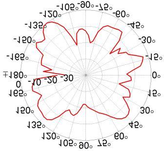
52 E-Plane 900 MHz 2 GHz 4 GHz 6 GHz H-Plane 900 MHz 2 GHz 4 GHz 6 GHz Figure 3.10: The E- and H-planes radiation patterns for different frequencies. 36
53 Chapter 4: Slot Antenna with Graded Index Superstrate 4.1 Approach I Graded Index Superstrate Design In addition to the off-centered, microstrip fed, slot antenna that creates a fictitious short circuit near the microstrip feed which produces a second resonance at a frequency slightly above the first resonance, another technique used to improve the bandwidth is to combine the slot antenna with a Dielectric Resonance Antenna (DRA). Dielectric resonance antennas are widely used in different antenna applications due to its low cost, wide band and high efficiency and inherently wide bandwidth [44]-[48]. Their designing process is flexible and are easy to integrate into any fabrication technology. It was observed that with proper design of the slot antenna and the DRA, a dual-band operation can be achieved by merging the two resonances of the slot antenna and the DRA. In order to further improve the bandwidth, a number of parasitic elements can also be added. Placement coplanar parasitic slot elements close to the slot antenna creates strong coupling among them which can lead to wideband operation [49] and [50]. It has been reported that adding a superstrate over a slot antenna can be used to reduce the antenna size and improve the antenna front-to-back ratio [51][52]. However, use of superstrtae for reducing the size of the slot antenna comes at the expense of narrower bandwidth. However, it has been shown that dimensions and dielectric constant of a finite superstrate can be designed in such 37
54 a way to excite a dielectric resonator mode that can easily be merged with that of the exciting slot antenna to achieve a dual mode operation [44]. To lower the quality factor of the dielectric resonator and achieve a higher bandwidth use of magneto-dielectric materials with permittivity almost equal to permeability was proposed in [53]. Such materials with low index contrast tend to present higher bandwidth. The drawback is the magnetic loss factor of the material that tends to lower the antenna efficiency at upper VHF and UHF bands. An alternative is to use graded index lens with high dielectric constant in contact with the slot antenna and lower dielectric near the top. The high dielectric in contact with the slot antenna can reduce the size of the slot antenna significantly and thus the slot antenna can only radiate effectively towards the superstrate direction leading to significant reduction in the backward radiation. It should however be noted that the backward radiation is also a function of the slot antenna ground plane size compared to the wavelength. The graded index allows a better matching to free-space and reduces the quality factor of the dielectric resonator. Due to the limitation of material availability, two different low-loss materials (glass and polycarbonate) are used as a stepped index superstrate. The dielectric constant of the glass and the polycarbonate used for the antenna design are measured to be 7.2 and 4 respectively. The thicknesses of both the glass and the polycarbonate layers are chosen according the material availability in the Radiation Laboratory to achieve the desired antenna response. Figure 4.1 (b) shows the side view of the slot antenna substrate with the glass and the polycarbonate superstrates and Figure 4.2 shows the perspective view of the slot antenna with the stepped index superstrate. 38
 Figure 4.1: a) The top view of the slot antenna.")
55 Ws =50mm Top view L =188mm w = 380mm l = 280mm (a) Polycarbonate substrate Side view 22mm Glass substrate Slot antenna substrate 72mm 0.5mm (b) Figure 4.1: a) The top view of the slot antenna. b) The side view of the slot antenna substrate and the graded index superstrate with dimensions. 39

56 22mm 72mm Polycarbonate substrate Glass substrate w = 380mm l = 280mm Figure 4.2: Slot antenna with a steppeded index superstrate. It was observed that adding the graded index superstrates on top of the slot antenna shifts the resonances to a lower frequency range since the size of the overall antenna is considered to be increased. The feed line is designed to improve the matching to 50Ω microstrip line. The frequency responses of the antenna return loss are shown in Figure 4.3 as the length of the slot antenna, L, is varied from 188 mm to 208 mm with 10 mm increment while the width remains the same, Ws = 50 mm. In Figure 4.4, the dimensions of the superstrate are varied. The nominal dimensions are: Length, l = 280 mm and the width, w = 380 mm. The dimensions of the slot antenna remain the same. In Figure 4.4, (a) shows the reflection coefficient of the slot antenna with the superstrate with the nominal dimensions of the superstrate, (b) shows the S11 when the width is reduced to w = 411 mm and the length, l was kept the same, (c) shows the S11 when the length is l = 309 mm and the width, was kept at w = 380 mm, and (d) shows the S11 when the length is l = 309 mm and the width is w = 411 mm. It is concluded that the upper resonance is affected by the superstrate dimensions. 40
 L = 208 mm. (c) L = 198 mm. S11,dB (a) (b) (c) (d) Frequency, MHz Figure 4.4: Length l and width w of the superstrate are varied. (a) Original dimensions, l = 280 mm, w = 380 mm.")
57 S11,dB (a) (b) (c) Frequency, MHz Figure 4.3: The reflection coefficient of the slot antenna with graded index superstrates. Length of the slot antenna is varied. (a) the original length L = 188 mm. (b) L = 208 mm. (c) L = 198 mm. S11,dB (a) (b) (c) (d) Frequency, MHz Figure 4.4: Length l and width w of the superstrate are varied. (a) Original dimensions, l = 280 mm, w = 380 mm. (b) l = 280 mm, w = 411 mm. (c) l = 309 mm, w = 380 mm. (d) l = 309 mm, w = 411 mm Parasitic Elements Effect So far it was demonstrated that using a wide slot antenna assisted by a fictitious short and suprestrate DRA can enhance the bandwidth. Another technique to further enhance the antenna bandwidth is to add parasitic elements. This technique has become more popular for its ability to 41
![improve the fundamental characteristics of an antenna such as polarization, gain, input impedance and radiation pattern [54] and [55]. Parasitic 1 Parasitic 3 Parasitic 2 Parasitic 4 Figure 4.](/docs-images/81/83198524/images/58-0.jpg "5: Top view of the slot antenna showing the four parasitic elements. Figure 4.")
58 improve the fundamental characteristics of an antenna such as polarization, gain, input impedance and radiation pattern [54] and [55]. Parasitic 1 Parasitic 3 Parasitic 2 Parasitic 4 Figure 4.5: Top view of the slot antenna showing the four parasitic elements. Figure 4.5 shows the slot antenna with four different possible parasitic elements around the slot antenna to increase the bandwidth at higher frequency band of operation. Placing the four parasitic elements close enough to the slot antenna creates strong coupling between the slot antenna and the parasitic elements. The location and dimensions of the four parasitic elements are chosen by trial and error method, using the Ansoft HFSS full wave simulator. Comparison between the reflection coefficients of the slot antenna with the stepped index superstrate and the inclusion of only one parasitic element at a time are shown in Figure 4.6. Figure 4.7 shows the reflection coefficients of the slot antenna with increasing inclusion of the parasitic elements. 42
59 S11,dB Without parasitic With parasitic # 1 With parasitic # 2 With parasitic # 3 With parasitic # 4 Frequency, MHz Figure 4.6: Comparison between the reflection coefficients of the slot antenna with each parasitic and without any parasitic. S11,dB With parasitic element # 1 With parasitic element # 1 and 2 With parasitic element # 1,2,and 3 With parasitic element # 1,2,3,and 4 Frequency, MHz Figure 4.7: Comparison between the reflection coefficients of the slot antenna with 1,2,3 and 4 parasitic elements. S11,dB With parasitic Without parasitic Frequency, MHz Figure 4.8: The reflection coefficient of the slot antenna with graded index superstrate without the parasitic elements and with four parasitic elements. 43
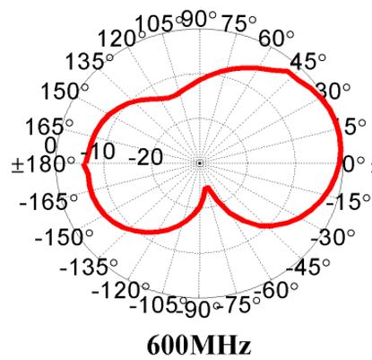
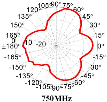
60 Figure 4.8 shows a comparison between the reflection coefficient of the slot antenna with the stepped index superstrate with and without the four parasitic elements. It was noticed that the reflection coefficient improves by adding the four parasitic elements around the slot antenna. The final design of the slot antenna is then fabricated Measurements and Results The prototype was fabricated on a Rogers RT/Duroid 5880 substrate with dielectric constant of 2.2 and 0.5mm thickness using the standard PCB technology. Glass and polycarbonate are used to assemble the graded index superstrates with tapered dielectric. The dielectric constant of the glass and the polycarbonate were measured to be 7.2 and 4 respectively. The thickness of the glass is 72mm and the thickness of the polycarbonate is 22mm. The dimensions of the antenna are 380mm x 280mm x 94mm. Four parasitic elements were added to improve the bandwidth. The dimensions of the parasitic elements were modified to achieve the required response. The superstrate, which consists of the glass and polycarbonate, is placed on top of the slot antenna as shown in Figure The reflection coefficient is then measured using a vector network analyzer. It shows that the antenna has a bandwidth of 35.5%. The measured reflection coefficient is compared with the simulate results as shown in Figure 4.9 where a good agreement between the simulation and measured results is observed. The deviation can be attributed to the fabrication process. An important feature of the wideband antenna is its gain and radiation pattern. Figure 4.10 shows the simulated and measured gain of the slot antenna. The gain was measured inside the anechoic chamber of the Radiation Laboratory at the University of Michigan. As can be seen in Figure 4.11, the electric field is concentrated in the upper half space which indicates that the radiation is taking place in the front side of the antenna. The back ratio is mainly due to finite size of the ground plane which is higher at lower frequencies. 44

61 S11,dB Simulated S11 Measured S11 Frequency, MHz Figure 4.9: The measured and simulated reflection coefficient of the slot antenna with graded index and four parasitic elements. Figure 4.10: The simulated and measured gain. Graded Index Superstrate Slot Antenna Figure 4.11: The electric field distribution of the slot antenna with graded index supserstrate and four parasitic elements at 400MHz. The concentration of fields in the superstrate indicates the directional radiation of the antenna. 45
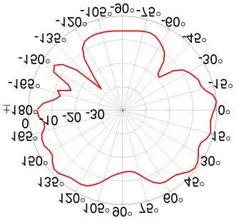
62 E-Plane H-Plane 230MHz 255MHz 230MHz 255MHz 330MHz 400MHz 330MHz 400MHz 450MHz 500MHz 450MHz 500MHz (a) (b) Figure 4.12: a) E-plane and b) H-plane radiation patterns of the final slot antenna design. 46


63 (a) (b) Figure 4.13: Final design Prototype 47

64 4.2 Approach II Stepped Index Superstrate Design In this section, very similar steps in designing the antenna to that in Approach I is followed. However, a superstrate with alternated dielectric constants, is used. The electromagnetic waves behavior can be controlled by adding different materials with different permittivities which allows better matching of the waves in the superstrate to the surrounding medium. Adding superstrate with equivalent dielectric constant of periodic media create a dielectric resonance mode near to the other resonance of the slot antenna itself. The superstrate has the effect of reducing the slot dimension for given resonance and therefore, the slot radiates effectively toward the superstrate and reduces the backward radiation. The stepped index allows a better matching to free-space. The width and length of the slot antenna and the thicknesses of each periodic layer of the superstrate are adjusted to achieve the required operating bandwidth. Figure 4.14 shows the side view of the slot antenna substrate with the glass and the polycarbonate superstrates. Figure 4.14: The side view of the slot antenna substrate and the stepped index superstrate. Similar to the previous design in Approach I, two parasitic elements are added to further enhance the bandwidth. Figure 4.15 (a) shows the slot antenna with two parasitic elements above the slot antenna to increase the bandwidth at higher frequency band of operation. Placing the two 48

 (b) Figure 4.")
65 parasitic elements close enough to the slot antenna creates strong coupling between the slot antenna and the parasitic elements. The location and dimensions of the two parasitic elements are determined by trial and error method, using the Ansoft HFSS full wave simulator. (a) (b) Figure 4.15: a) The top view of the slot antenna showing the two parasitic elements. b) The side view of the slot antenna substrate and the graded index superstrate with dimensions. 49
66 4.2.2 Measurements and Results The antenna was fabricated on a Rogers RT/Duroid 5880 substrate with dielectric constant of 2.2 and 0.5mm thickness using the standard PCB technology. The dielectric constant of the glass and the polycarbonate were measured to be 7.2 and 4 respectively. The thickness of each glass layer is 12.7mm and the thickness of each polycarbonate layer is 4.5mm. Different simulations with different numbers of glass polycarbonate layers were performed. Figure 4.16 show the VSWR of the slot antenna with: 86mm, 110mm, 130mm and 150mm superstrate thickness for comparison purposes. 5 layers of Glass and 5 layers polycarbonate are used to assemble the superstrates with stepped dielectric. Therefore, stepped superstrate thickness used is 86mm. Two parasitic elements were added to improve the bandwidth. The dimensions of the parasitic elements were adjusted to achieve the required response. The superstrate is placed on top of the slot antenna as shown in Figure 4.15 (b). Figure 4.17 shows a comparison of the VSWR between the slot antenna with the stepped dielectric superstrate and with the graded index superstrate. The VSWR is then measured using a calibrated HP8720D vector network analyzer. This antenna has a bandwidth of 33.3%. The measured VSWR is compared with the simulate results as shown in Figure 4.18 where a good agreement between the simulation and measured results is observed. The deviation can be attributed to the fabrication process.. Figure 4.19 shows the radiation pattern of the E-plane and H plane. It can be noticed that the radiation is taking place in the front side of the antenna. The back ratio is mainly due to finite size of the ground plane which is higher at lower frequencies. 50
67 Figure 4.16: comparison of VSWR of the slot antenna with different stepped dielectric superstrate thicknesses. Figure 4.17: VSWR Comparison between the slot antenna with stepped dielectric superstrate and with graded index superstrate. Figure 4.18: measured and simulated VSWR of the slot antenna with stepped dielectric superstrate and two parasitic elements. 51


68 Figure 4.19: E-plane and H-plane radiation patterns of the final slot antenna design. 52


69 (a) (b) Figure 4.20: Final design Prototype. 53


70 The fabricated slot antenna with a superstrate is then placed directly on sand available in the radiation laboratory at the University of Michigan. Another approach is to add a Styrofoam between the sand and the fabricated antenna as can be seen in Figure The reflection coefficients of the antenna placed on the sand itself and sand with Styrofoam are illustrated in Figure As can be seen from the figure, there is 10dB difference between the measured antenna and the measured antenna over the sand. However, by knowing the dielectric constant of the sand, the superstrate design can be slightly changed in order to be matched to the given sand. (a) (b) Figure 4.21: fabricated antenna on top of; a) sand. b) Sand and Styrofoam. 54
 sand. 2) Sand and Styrofoam.")

71 S11,dB Frequency, MHz final design on top of sand on top of sand and styrofoam 1 on top of sand and styrofoam 2 Figure 4.22: Comparison of the measured reflection coefficients of the fabricated antenna on top 1) sand. 2) Sand and Styrofoam. Another Layer of concrete between the antenna and the sand is added (Figure 4.23). Figure 4.24 shows the reflections coefficient differences between antenna itself, placing the antenna over sand and concrete, and placing the antenna over sand, concrete and Styrofoam. (a) (b) Figure 4.23: fabricated antenna on top of; a) sand and concrete. b) Sand, concrete, and Styrofoam. 55
72 S11,dB Final design on top of sand and concrete on top of sand, concrete and styrofoam Frequency, MHz Figure 4.24: Comparison of the measured reflection coefficients of the fabricated antenna on top 1) sand and concrete. 2) Sand, concerete, and styrofoam. 56
73 Chapter 5: Miniaturized Omnidirectional Horizontally Polarized Wire-Loop Antenna 5.1 Background In addition to the three factors in antenna miniaturization mentioned in sections 1.2.2, generation of a desired polarization or a specific radiation pattern for many application where polarization or radiation diversity are utilized are important. If a horizontal polarization with omnidirectional radiation is desired, a small loop antenna, which the dual of vertical short dipole antenna, can be utilized [56]. However, small loop antennas similar to small dipole antennas are difficult to impedance match to a 50 Ohm line. Use of external matching network may lead to poor radiation efficiency or a bulky antenna structure. Different approaches to reduce antenna size have been reported [57]. One technique to design miniaturized dipole antennas is to meander the wire [58] and [59], however; this approach leads to poor radiation efficiency as the opposite flow of electric current in the meander wire cancel the radiated field from adjacent segments. It is shown in [60]-[62] how the meandering approach can be applied to slot antennas. However, using meandering technique will make the antenna very hard to match to a 50Ω line. Very small slot antennas with very high radiation efficiency that do not require external matching network are reported in [[30], [50] and [63]]. Theoretically slot antennas (with infinite ground plane) should produce omni-directional radiation pattern in E-plane. However, small size slot antennas with finite ground planes produce a null radiation in along the ground plane direction. It is the intent of 57
74 this paper to present a small size, low profile, horizontally polarized antenna with omnidirectional radiation pattern that does not require external matching network. Recently, the concept of composite slot loop antenna was introduced to develop a low-profile antenna that can produce a vertical polarization [64]. This antenna design is inspired from a small magnetic loop using a slot configuration on metallic a small ground. For miniaturization purposes, the meandering approach employed in [30] and [63] was utilized to reduce the size of six driven elements around the circumference of a small circle.. The size of this omnidirectional miniaturized antenna can be as small as λ/10 and its height can be as small as λ/60. Since the input impedance of short slot antennas is rather high the elements could be fed in parallel, but series capacitors at the feed point had to be used to achieve the impedance match. 5.2 Antenna Design It is well-known that a small circular loop can produce horizontally polarized omnidirectional radiation pattern. However, a major drawback of this antenna is its extremely low radiation resistance, proportional to ( a λ )4, which is given by [56]: R loop = 320π 6 ( a λ )4 (9) where, a is the radius of the loop. This low radiation resistance leads to very poor radiation efficiency. Although the radiation resistance can be improved using multi-turn loop (by factor of N 2 ), the additional ohmic resistance and the resulting higher inductance keeps the radiation efficiency low and impedance matching more difficult. To increase the radiation resistance, the radiated power, which is proportional to the loop current squared, the current in the loop must be increased. This can be accomplished by packing resonant dipole antennas within a circle. To ensure omni-directional radiation, the current around the perimeter of the enclosing circle must be almost 58
75 a constant and not canceled by any opposing current. Applying the meandering approach and fold the edge of a half-wavelength dipole antenna into a spiral-like shape reduces the dipole length significantly. Placing these meandered dipole antennas around the circumference of a small circle creates the desired wire-loop antenna as shown in Figure 5.1. It is noted that the circumferential currents, constituted from three diploes, are all in the same direction and almost uniformly distributed around the circle. This is due to the fact that the electric current on a dipole at resonance is strong and almost constant near the feed point. Also feeding the dipoles identically with proper polarity, not only the circumferential currents are uniform around the circle, but also the radiations from the spiral arms of the adjacent dipoles cancel each other. This will cause radiation to only come from the strong circumferential currents as it the case for small wire loop antennas. Figure 5.1: Composite wire-loop antenna. (a) 59
76 (b) Figure 5.2: Real and imaginary parts of the input impedance of: a) one short dipole with end spirals and, b) three short dipoles. The challenges are in the feed network and impedance matching. Short dipole antennas with end spirals have low radiation resistance and rapidly varying reactance at the resonance as shown in Figure 5.2 (a). The terminal is placed right at the middle of the dipole and its physical parameters are as follows: l = 308mm, t = 0.3mm, and h=0.5mm where l is the dipole length and t is the trace width, and h is the substrate thickness with dielectric constant of 2.2. Due to the proximity of the end-spirals, the input impedance and the resonant frequency of a short dipole in the presence of the other dipoles in the composite loop are quite different than the isolated antenna. The input impedance of the dipole of Figure 5.1 in the presence of two other similar antennas terminated with matched load 50Ω is shown in Figure 5.2 (b). One advantage of adjacent elements is that they significantly improve the input resistance and decrease the rate of change of reactance with frequency which leads to higher bandwidth. The most convenient way to feed the antennas is the parallel feeding. Unfortunately, feeding the antenna in parallel fashion will further reduce its input impedance, and matching this antenna to a 50Ω-line becomes very difficult. A better approach is to feed the three antennas in series. This way the radiation 60


77 resistances are added and gets closer to the transmission line characteristic impedance. In addition the line thickness and the length of the two wire transmission lines between the dipole terminals and the feed point in the center of the loop can be used for impedance matching as well. To facilitate series feeding approach, the antenna can be fabricated on three layers as shown in Figure 5.3. Metallic via holes can be used to connect the transmission lines to the dipole traces on different layers. Top layer - + 1mm Antenna feed Middle layer bottom layer Figure 5.3: Three layers composite-wire loop antenna. Through extensive numerical optimization it is found that the structure of Figure 5.3 cannot be matched to a 50Ω line exactly. The main problem is the low radiation resistance of the dipoles. One approach is to increase the number of dipoles within the circle. For a given loop radius, each dipole has to be further miniaturized, but this will lead to a very small bandwidth if the antenna could be matched. A better approach for increasing the input impedance is to increase the input impedance of each element using the folded antenna topology. For ordinary dipole antennas the input impedance can be increased with the square of the number of folds. So if there are N parallel 61
![wires forming the multi-folded dipole, the input impedance is increased by N 2 [65]. The geometry of Figure 5.](/docs-images/81/83198524/images/78-0.jpg "3 is designed and modified for 2-, 3-, and 4-folded short dipoles for the composite loop antenna topology. Figure 5.4 shows the antenna geometry for the 4-folded short dipole configuration.")
78 wires forming the multi-folded dipole, the input impedance is increased by N 2 [65]. The geometry of Figure 5.3 is designed and modified for 2-, 3-, and 4-folded short dipoles for the composite loop antenna topology. Figure 5.4 shows the antenna geometry for the 4-folded short dipole configuration. Also Figure 5.5 shows the input reflection coefficients at the feed point of the antenna for 2-, 3-, and 4-folded configurations. As observed the input impedance of the folded structure can be better matched with higher bandwidth when the number of folds increased. The shift in the resonant frequency is the result of change in the mutual coupling between the adjacent elements. It should be emphasized that the diameter of 4-folded configuration is less than λ/9 at the resonant frequency. The simulated gain of the antenna is 0.2dB and its radiation efficiency is 90% which is by may order of magnitude higher than the conventional small loop antennas. Figure 5.4: Folded Composite wire-loop antenna. 62

79 S11, db 2 folded segments 3 folded segments 4 folded segements Frequency, MHz Figure 5.5: The reflection coefficient of the composite wire-loop antenna with different folding numbers. Figure 5.6: The current distribution over the composite loop antenna. 5.3 Antenna Feed Connecting a dipole antenna directly to a coaxial cable induces electric current over the outer layer of the coaxial cable which in turn can cause radiation and unbalanced current distribution on the dipole arms. A transformer with a center-tap terminal of its secondary coil connected to the outer connector of the input coaxial line which is connected to the primary coil of the transformer, 63
80 produces a balance terminal (the transformer secondary) for the dipole. The advantages of transformer-type baluns is their compact size and light weight which make them ideal for application at HF-UHF bands [65] and [66]. This is important as the size of the antenna is very small compared to the wavelength. For lower frequency applications, the size of transmission line baluns are quite large (>λ/4) and cannot be used. Therefore, an isolated balanced to unbalanced transformer is suggested and used. In this design, a 3.8mmx3.8mm mini wideband transformer from coilcraft, WBC1-1TLB, with 1:1 impedance ratio and 0.58dB insertion loss is used. Due to space limitation, a MMCX jack connector is used instead of a regular SMA connector. This connector is then connected to MMCX to SMA adapter for cable connections during measurements. 5.4 Measurements and Results The designed antenna is fabricated on a 0.5mm thick RT/Duroid5880. This substrate has a dielectric constant of 2.2 and loss tangent of Two parts of the proposed antenna were fabricated on opposite sides of one substrate. The third part of the antenna was fabricated on a second substrate which is then limited to the first substrate. The fabricated antenna overall diameter is 77.6mm with a height of 1mm. Figure 5.7 shows the top view of the antenna final design with dimensions. Figure 5.8 shows the final design prototype. The figure shows each layer individually since each layer is on a different substrate surface. 64


81 0.3mm 0.3mm 77.6mm Figure 5.7: The composite wire-loop antenna with the transformer and MMCX jack connector pads. Figure 5.8: The prototype of the composite wire-loop antenna. The reflection coefficient of the fabricated antenna is measured using a calibrated HP8720D vector network analyzer. Figure 5.9 shows the measured and simulated reflection coefficients. It 65
82 S11, db is shown that the measured result is in a good agreement with the simulation. However, the deviation can be attributed to the fabrication process. The radiation pattern is measured using the University of Michigan Radiation Laboratory anechoic chamber. Figure 5.10 shows the measured radiation pattern of the composite wire-loop antenna in the E and H planes and as expected the farfiled radiation pattern very closely resembles that of a small dipole. The radiation pattern in E- plane is uniform to within ±0.25dB. Also the antenna gain is measured to be 0dBi. Comparing the measured gain with the directivity of an ideal small loop antenna (1.75dB), the antenna radiation efficiency (including the balun loss) is found to be 67% which is far better than conventional small loop antennas. Measured S11 Simulated S11 Frequency, MHz Figure 5.9: The measured and simulated reflection coefficients of the composite wire-loop antenna. E-Plane (a) 66
83 H-Plane (b) Figure 5.10: The measured radiation pattern of the composite wire-loop antenna. a) E-Plane. b) H-Plane. 67
84 Chapter 6: A compact, Wideband Array of Coupled Quarter-Wavelength Slot Antenna for the 700MHz band 6.1 Quarter wavelength slot antenna A relatively new approach to reduce the slot antenna dimensions is to shorten the antenna length to λ/4 instead of λ/2 and have one edge open. This new approach is similar to the inverted- F antenna. Quarter-wavelength slot antenna is also called monopole slot antenna [67] and [68]. A λ/4 slot antenna with one end open circuited and the other short-circuited is fed by a microstrip feed line and used as the driving element is presented. This antenna is based on the basic halfwavelength slot antennas. The mechanism of designing the quarter-wavelength slot antenna is to use one half of the half-wavelength slot antenna and to have one of the slot edges as an open circuit. Using this concept, the size of the antenna is reduced by half and the resonant frequency is remained unchanged. A number of λ/4 slot antennas are appropriately position around the driving element to achieve the required bandwidth. An advantage of this design is that active circuit components can be place on the top side of the substrate that supports the microstrip line as long as the slots are not covered or crossed by RF lines. 6.2 Antenna design A quarter-wavelength slot antenna is based on the basic half-wavelength slot antenna. A resonance can be achieved if half of the half-wavelength slot antenna is used. This supports the 68
.")
85 maximum voltage at the open end and a voltage node at the short circuit end. Unlike quarter-wave monopole antennas that require a ground plane, quarter-wave slot can easily be realized on a finite ground plane as shown in Figure 6.1 (a). Similar to half-wavelength slot antennas can be easily excited and matched to a wide range line impedances, by a microstrip line crossing the slot near one end. The closer the line crossing point to the short-circuited end, the lower the input impedance will get. The reactance of the slot antenna can also easily be compensated by choosing the length of the open-ended mircostrip line extending beyond the slot crossing point. Figure 6.1 illustrates a λ/4 slot antenna design that has a center frequency at 700MHz as can be seen from the reflection coefficient shown in Figure 6.1 (b). However, the location and dimension of the microstrip feed line was adjusted using the Ansoft HFSS simulator to achieve the desired resonant frequency. This response is similar to the response of the conventional λ/2 slot operating in the same frequency. λ/4 (a) 69
86 S11, db Frequency, MHz (b) Figure 6.1: a) Quarter-wavelength slot antenna design. b) The reflection coefficient of the quarter-wavelength slot antenna. 6.3 Double-element quarter-wavelength slot antenna Enhancing the bandwidth by using a double-element conventional slot antenna was studied and reported in [43]. In this section, two quarter-wavelength slot antennas, operating at slightly different frequencies, using a single microstrip feed line to feed both slot antennas is presented. This topology is similar to the multi-band microstrip feed line slot antenna discussed in section 3.2. As mentioned in section 3.2.1, there are number of different multi-element feeding topologies. The parallel feed topology is a great alternative for multi-element antenna since it provides better flexibility in designing the feeding network as it makes the antenna impedance matching easier to be achieved. Figure 6.3 shows the geometry of a two-element quarter-wavelength slot antenna fed in parallel with a microrstrip line. The impedance match and the resonant frequencies are achieved by the feeding line cross points, the open-ended microstrip stub lengths, and the length of the slot antenna elements. 70

87 Figure 6.2: Quarter-wavelength double-element slot antenna design. A third resonant is near 800 MHz, shown Figure 6.3, is also observed. This was initially assumed to have been generated from a fictitious short circuit reported in [43]. Under certain conditions, microstrip fed slot antennas can produce two resonances. This second resonance is attributed to a fictitious short circuit within the slot generated from the cancellation of field produced by the feeding line and the field of the slot line. Our attempts to generate such resonance in quarter-wavelenght slot antennas were not successful. Running more simulations, it is found out that the additional resonance remains even after removing the second λ/4 slot antenna while keeping the second microstrip feeding line as can be seen in Figure 6.4. It is suggested that the additional feed line leg is effecting the impedance matching which create the third resonant at a higher frequency. Figure 6.5 shows the reflection coefficient of a single λ/4 slot antenna with different length values of the additional microstrip feed line. As can be seen from this figure, changing the length of the feed line changes the antenna input impedance. 71
 Single quarter-wavelength slot antenna with additional feed line.")
88 S11, db Frequency, MHz Figure 6.3: The reflection coefficient of the quarter-wavelength double-element slot antenna l lstub (a) S11, db Frequency, MHz (b) Figure 6.4: a) Single quarter-wavelength slot antenna with additional feed line. b) The reflection coefficient of the quarter-wavelength slot antenna with the additional feed line. 72

89 S11, db 41mm 40mm 42mm Frequency, MHz Figure 6.5: The reflection coefficient of the quarter-wavelength slot antenna with different lengths of the additional feed line. To get a better impedance-matched condition, the length of the second microstrip line is adjusted. This is interesting as it is shown that an open-ended microstrip line can make the impedance matching possible at two frequencies. One of the popular matching approaches is to use an open-circuited stub of appropriate length at an appropriate distance from a load [69]. There are two adjustable parameters in the shunt stub topology, the distance from the load to the shunt stub (l) and the shunt length (lstub) as illustrated in Figure 6.4 (a). Figure 6.7 shows the input impedance of the microstrip line as a function of frequency without adding the shunt stub as demonstrated in Figure 6.6. For wideband operation a frequency near the end of the band is considered and stub matching approach is used to match the antenna at that frequency. Zl 73
90 Figure 6.6: Single λ/4 slot antenna design showing the input impedance, Zl, location. a (a) is at 700MHz Figure 6.7: Smith chart of single λ/4 slot antenna design. Both distances, l and lstub, were optimized to improve the matching at the beginning and the end of the desired band of operation. Figure 6.8 shows how the antenna impedance as a function of frequency with two impedance matched frequencies of 695MHz and 821MHz. b a (a) is at 695MHz (b) is at 821MHz Figure 6.8: Smith chart of single λ/4 slot antenna design with the shunt stub. 74

91 6.4 Bandwidth enhancement with additional parasitic elements Another technique to increase the antenna bandwidth is to add parasitic elements. A number of λ/4 slot antennas are appropriately positioned around the driving element to achieve the required bandwidth. The entire structure is designed over a finite ground plane whose dimensions also affect the resonant frequencies and eventually the overall bandwidth of the antenna. As shown in Figure 6.4, an open stub is needed to get a resonance at the upper portion of the band. To eliminate the possibility of interaction of this stub with other parasitic elements, the microstrip stub is meandered in a corner as shown in Figure 6.9. Figure 6.9 (a) illustrate the λ/4 slot antenna with one parasitic element while Figure 6.9 (b) shows the effect of the single parasitic element on the antenna s reflection coefficient. The parasitic element s length and separation from the driven element are adjusted to achieve the second resonance. As can be seen, the meandered microstrip stub is also creating the third resonant at 830MHz. 99mm 72mm 2.5mm 60mm (a) 75
92 S11, db Frequency, MHz (b) Figure 6.9: a) λ/4 slot antenna with single parasitic element. b) The reflection coefficient of the λ/4 slot antenna with single parasitic element. To fill the spectrum with resonance and achieve a wideband, more parasitic elements are needed. The location and the number of elements are determined from the current distribution on the ground plane. After extensive numerical optimization, it is noticed that changing the length of the microstrip stub not only affects the location of the resonant frequency created by this stub, but also affects the location of the other resonances created by the parasitic elements. This is due to the fact that the reactance of the driven slot antenna is affected by the presence of the parasitic elements. Figure 6.10 shows the input reflection coefficient of the slot antenna with different numbers of parasitic elements. The number of resonances observed is equal to number of parasitic elements plus two. One resonance is due to the driven elements and the other is due to the mirostrip stub. It is noted here that the antenna parameters with 1, 2, or 3 parasitics are optimized individually arrive at the results shown in Figure It turned out that to achieve the required bandwidth 4 parasitic elements are required. 76

93 S11, db With 3 parasitics With 2 parasitics With 1 parasitic Frequency, MHz Figure 6.10: The reflection coefficient of the λ/4 slot antenna with different parasitic element numbers. S11, db 44mm 43mm 45mm Frequency, MHz Figure 6.11: The reflection coefficients of the λ/4 slot antenna with 3 parasitic elements and different additional feed line leg lengths. Figure 6.11 shows how changing the length of the additional microstrip feed line effects antenna input impedance. A fourth parasitic element is added close to the existed three parasitic 77

94 elements. Figure 6.12 shows the configuration of the final design. The input impedance of this antenna with 6 resonances is shown Figure Figure 6.12: The final design of the λ/4 slot antenna with 4 parasitic elements. Figure 6.13: The simulated reflection coefficient of the λ/4 slot antenna with 4 parasitic elements. 6.5 Measurements and Results The designed antenna is fabricated on a 0.8mm thick FR-4 substrate. This substrate has a dielectric constant of 4.4 and loss tangent of Both sides of the substrate were used, top side for the slot antenna with all four parasitic elements and the bottom side for the microstrip feed line. The overall dimension of the substrate is 99mm x 60mm x 0.8mm. Figure 6.14 shows the fabricated antenna size, top and bottom views, compared to an Apple iphone. 78


95 Figure 6.14: Top and bottom views of the fabricated quarter-wavelength slot antenna next to an Apple iphone device. The reflection coefficient of the fabricated antenna is then measured using a calibrated HP8720D vector network analyzer. Figure 6.15 shows the measured and simulated reflection coefficients. It is shown that the measured results are in a good agreement with the simulation. However, the small differences between the measured and simulated reflection coefficient can be related to the fabrication process. Figure 6.16 shows the measured gain is in a good agreement with the simulations as well. The radiation pattern is also measured using the University of Michigan Radiation Laboratory anechoic chamber. Figure 6.17 (a) and (b) show the measured radiation pattern of the proposed antenna in the E and H planes respectively. 79
COUPLED SECTORIAL LOOP ANTENNA (CSLA) FOR ULTRA-WIDEBAND APPLICATIONS *
 FOR ULTRA-WIDEBAND APPLICATIONS *") COUPLED SECTORIAL LOOP ANTENNA (CSLA) FOR ULTRA-WIDEBAND APPLICATIONS * Nader Behdad, and Kamal Sarabandi Department of Electrical Engineering and Computer Science University of Michigan, Ann Arbor, MI,
COUPLED SECTORIAL LOOP ANTENNA (CSLA) FOR ULTRA-WIDEBAND APPLICATIONS * Nader Behdad, and Kamal Sarabandi Department of Electrical Engineering and Computer Science University of Michigan, Ann Arbor, MI,
Coupled Sectorial Loop Antenna (CSLA) for Ultra Wideband Applications
 for Ultra Wideband Applications") Coupled Sectorial Loop Antenna (CSLA) for Ultra Wideband Applications N. Behdad and K. Sarabandi Presented by Nader Behdad at Antenna Application Symposium, Monticello, IL, Sep 2004 Email: behdad@ieee.org
Coupled Sectorial Loop Antenna (CSLA) for Ultra Wideband Applications N. Behdad and K. Sarabandi Presented by Nader Behdad at Antenna Application Symposium, Monticello, IL, Sep 2004 Email: behdad@ieee.org
A Broadband Omnidirectional Antenna Array for Base Station
 Progress In Electromagnetics Research C, Vol. 54, 95 101, 2014 A Broadband Omnidirectional Antenna Array for Base Station Bo Wang 1, *, Fushun Zhang 1,LiJiang 1, Qichang Li 2, and Jian Ren 1 Abstract A
Chapter 7 Design of the UWB Fractal Antenna
 Chapter 7 Design of the UWB Fractal Antenna 7.1 Introduction F ractal antennas are recognized as a good option to obtain miniaturization and multiband characteristics. These characteristics are achieved
Antenna Theory and Design
 Antenna Theory and Design Antenna Theory and Design Associate Professor: WANG Junjun 王珺珺 School of Electronic and Information Engineering, Beihang University F1025, New Main Building wangjunjun@buaa.edu.cn
ANALYSIS OF ELECTRICALLY SMALL SIZE CONICAL ANTENNAS. Y. K. Yu and J. Li Temasek Laboratories National University of Singapore Singapore
 Progress In Electromagnetics Research Letters, Vol. 1, 85 92, 2008 ANALYSIS OF ELECTRICALLY SMALL SIZE CONICAL ANTENNAS Y. K. Yu and J. Li Temasek Laboratories National University of Singapore Singapore
DESIGN OF A NOVEL WIDEBAND LOOP ANTENNA WITH PARASITIC RESONATORS. Microwaves, Xidian University, Xi an, Shaanxi, China
 Progress In Electromagnetics Research Letters, Vol. 37, 47 54, 2013 DESIGN OF A NOVEL WIDEBAND LOOP ANTENNA WITH PARASITIC RESONATORS Shoutao Fan 1, *, Shufeng Zheng 1, Yuanming Cai 1, Yingzeng Yin 1,
A Compact Dual Band-Notched Ultrawideband Antenna with λ/4 Stub and Open Slots
 Progress In Electromagnetics Research C, Vol. 49, 133 139, 2014 A Compact Dual Band-Notched Ultrawideband Antenna with λ/4 Stub and Open Slots Jian Ren * and Yingzeng Yin Abstract A novel compact UWB antenna
CHAPTER 5 PRINTED FLARED DIPOLE ANTENNA
 CHAPTER 5 PRINTED FLARED DIPOLE ANTENNA 5.1 INTRODUCTION This chapter deals with the design of L-band printed dipole antenna (operating frequency of 1060 MHz). A study is carried out to obtain 40 % impedance
CHAPTER 4 DESIGN OF BROADBAND MICROSTRIP ANTENNA USING PARASITIC STRIPS WITH BAND-NOTCH CHARACTERISTIC
 CHAPTER 4 DESIGN OF BROADBAND MICROSTRIP ANTENNA USING PARASITIC STRIPS WITH BAND-NOTCH CHARACTERISTIC 4.1 INTRODUCTION Wireless communication technology has been developed very fast in the last few years.
Circular Patch Antenna with CPW fed and circular slots in ground plane.
 Circular Patch Antenna with CPW fed and circular slots in ground plane. Kangan Saxena, USICT, Guru Gobind Singh Indraprastha University, Delhi-75 ---------------------------------------------------------------------***---------------------------------------------------------------------
THE recent allocation of frequency band from 3.1 to
 IEEE TRANSACTIONS ON ANTENNAS AND PROPAGATION, VOL. 54, NO. 11, NOVEMBER 2006 3075 Compact Ultrawideband Rectangular Aperture Antenna and Band-Notched Designs Yi-Cheng Lin, Member, IEEE, and Kuan-Jung
New Design of CPW-Fed Rectangular Slot Antenna for Ultra Wideband Applications
 International Journal of Electronics Engineering, 2(1), 2010, pp. 69-73 New Design of CPW-Fed Rectangular Slot Antenna for Ultra Wideband Applications A.C.Shagar 1 & R.S.D.Wahidabanu 2 1 Department of
Research Article A Very Compact and Low Profile UWB Planar Antenna with WLAN Band Rejection
 e Scientific World Journal Volume 16, Article ID 356938, 7 pages http://dx.doi.org/1.1155/16/356938 Research Article A Very Compact and Low Profile UWB Planar Antenna with WLAN Band Rejection Avez Syed
A Wideband Dual-polarized Modified Bowtie Antenna for 2G/3G/LTE Base-station Applications
 Progress In Electromagnetics Research Letters, Vol. 61, 131 137, 2016 A Wideband Dual-polarized Modified Bowtie Antenna for 2G/3G/LTE Base-station Applications Zhao Yang *, Cilei Zhang, Yingzeng Yin, and
Antenna Design for Ultra Wideband Application Using a New Multilayer Structure
 PIERS ONLINE, VOL. 2, NO. 6, 2006 544 Antenna Design for Ultra Wideband Application Using a New Multilayer Structure Yashar Zehforoosh, Changiz Ghobadi, and Javad Nourinia Department of Electrical Engineering,
COMPACT SLOT ANTENNA WITH EBG FEEDING LINE FOR WLAN APPLICATIONS
 Progress In Electromagnetics Research C, Vol. 10, 87 99, 2009 COMPACT SLOT ANTENNA WITH EBG FEEDING LINE FOR WLAN APPLICATIONS A. Danideh Department of Electrical Engineering Islamic Azad University (IAU),
APPLICATION NOTE FOR PA.700A ANTENNA INTEGRATION
 APPLICATION NOTE FOR PA.700A ANTENNA INTEGRATION VERSION A Your Global Source for RF, Wireless & Energy Technologies www.richardsonrfpd.com 800.737.6937 630.208.2700 APN-11-8-001/A 14-July-11 Page 1 of
CPW- fed Hexagonal Shaped Slot Antenna for UWB Applications
 International Journal of Information and Computation Technology. ISSN 0974-2239 Volume 3, Number 10 (2013), pp. 1015-1024 International Research Publications House http://www. irphouse.com /ijict.htm CPW-
Loop and Slot Antennas
 Loop and Slot Antennas Prof. Girish Kumar Electrical Engineering Department, IIT Bombay gkumar@ee.iitb.ac.in (022) 2576 7436 Loop Antenna Loop antennas can have circular, rectangular, triangular or any
UNIVERSITI MALAYSIA PERLIS
 UNIVERSITI MALAYSIA PERLIS SCHOOL OF COMPUTER & COMMUNICATIONS ENGINEERING EKT 341 LABORATORY MODULE LAB 2 Antenna Characteristic 1 Measurement of Radiation Pattern, Gain, VSWR, input impedance and reflection
Design of Star-Shaped Microstrip Patch Antenna for Ultra Wideband (UWB) Applications
 Applications") Design of Star-Shaped Microstrip Patch Antenna for Ultra Wideband (UWB) Applications Mustafa Abu Nasr 1, Mohamed K. Ouda 2 and Samer O. Ouda 3 1 Engineering Department, Al Azhar University, Gaza, Palestine,
Design of Star-Shaped Microstrip Patch Antenna for Ultra Wideband (UWB) Applications Mustafa Abu Nasr 1, Mohamed K. Ouda 2 and Samer O. Ouda 3 1 Engineering Department, Al Azhar University, Gaza, Palestine,
A Very Wideband Dipole-Loop Composite Patch Antenna with Simple Feed
 Progress In Electromagnetics Research Letters, Vol. 60, 9 16, 2016 A Very Wideband Dipole-Loop Composite Patch Antenna with Simple Feed Kai He 1, *, Peng Fei 2, and Shu-Xi Gong 1 Abstract By combining
SINGLE-FEEDING CIRCULARLY POLARIZED TM 21 - MODE ANNULAR-RING MICROSTRIP ANTENNA FOR MOBILE SATELLITE COMMUNICATION
 Progress In Electromagnetics Research Letters, Vol. 20, 147 156, 2011 SINGLE-FEEDING CIRCULARLY POLARIZED TM 21 - MODE ANNULAR-RING MICROSTRIP ANTENNA FOR MOBILE SATELLITE COMMUNICATION X. Chen, G. Fu,
Antennas Prof. Girish Kumar Department of Electrical Engineering Indian Institute of Technology, Bombay. Module 2 Lecture - 10 Dipole Antennas-III
 Antennas Prof. Girish Kumar Department of Electrical Engineering Indian Institute of Technology, Bombay Module 2 Lecture - 10 Dipole Antennas-III Hello, and welcome to todays lecture on Dipole Antenna.
Triple Band-Notched UWB Planar Monopole Antenna Using Triple-Mode Resonator
 Progress In Electromagnetics Research C, Vol. 57, 117 125, 215 Triple Band-Notched UWB Planar Monopole Antenna Using Triple-Mode Resonator Huaxia Peng 1, 3, Yufeng Luo 1, 2, *, and Zhixin Shi 1 Abstract
Design of Frequency and Polarization Tunable Microstrip Antenna
 Design of Frequency and Polarization Tunable Microstrip Antenna M. S. Nishamol, V. P. Sarin, D. Tony, C. K. Aanandan, P. Mohanan, K. Vasudevan Abstract A novel compact dual frequency microstrip antenna
Compact and Low Profile MIMO Antenna for Dual-WLAN-Band Access Points
 Progress In Electromagnetics Research Letters, Vol. 67, 97 102, 2017 Compact and Low Profile MIMO Antenna for Dual-WLAN-Band Access Points Xinyao Luo *, Jiade Yuan, and Kan Chen Abstract A compact directional
A Compact Dual-Polarized Antenna for Base Station Application
 Progress In Electromagnetics Research Letters, Vol. 59, 7 13, 2016 A Compact Dual-Polarized Antenna for Base Station Application Guan-Feng Cui 1, *, Shi-Gang Zhou 2,Shu-XiGong 1, and Ying Liu 1 Abstract
Compact UWB Planar Antenna with Triple Band EMI Reduction Characteristics for WiMAX/WLAN/X-Band Satellite Downlink Frequency
 Progress In Electromagnetics Research M, Vol. 1, 13 131, 17 Compact UWB Planar Antenna with Triple Band EMI Reduction Characteristics for WiMAX/WLAN/X-Band Satellite Downlink Frequency Priyanka Usha *
A NOVEL COMPACT ARCHIMEDEAN SPIRAL ANTENNA WITH GAP-LOADING
 Progress In Electromagnetics Research Letters, Vol. 3, 169 177, 2008 A NOVEL COMPACT ARCHIMEDEAN SPIRAL ANTENNA WITH GAP-LOADING Q. Liu, C.-L. Ruan, L. Peng, and W.-X. Wu Institute of Applied Physics University
Broadband Circular Polarized Antenna Loaded with AMC Structure
 Progress In Electromagnetics Research Letters, Vol. 76, 113 119, 2018 Broadband Circular Polarized Antenna Loaded with AMC Structure Yi Ren, Xiaofei Guo *,andchaoyili Abstract In this paper, a novel broadband
Chapter 2. Modified Rectangular Patch Antenna with Truncated Corners. 2.1 Introduction of rectangular microstrip antenna
 Chapter 2 Modified Rectangular Patch Antenna with Truncated Corners 2.1 Introduction of rectangular microstrip antenna 2.2 Design and analysis of rectangular microstrip patch antenna 2.3 Design of modified
A Wideband Magneto-Electric Dipole Antenna with Improved Feeding Structure
 ADVANCED ELECTROMAGNETICS, VOL. 5, NO. 2, AUGUST 2016 ` A Wideband Magneto-Electric Dipole Antenna with Improved Feeding Structure Neetu Marwah 1, Ganga P. Pandey 2, Vivekanand N. Tiwari 1, Sarabjot S.
ISSN: [Sherke* et al., 5(12): December, 2016] Impact Factor: 4.116
![ISSN: [Sherke* et al., 5(12): December, 2016] Impact Factor: 4.116](/thumbs/86/93220221.jpg "ISSN: [Sherke* et al., 5(12): December, 2016] Impact Factor: 4.116") IJESRT INTERNATIONAL JOURNAL OF ENGINEERING SCIENCES & RESEARCH TECHNOLOGY COMPACT ULTRA WIDE BAND ANTENNA WITH BAND NOTCHED CHARACTERISTICS. Raksha Sherke *, Ms. Prachi C. Kamble, Dr. Lakshmappa K Ragha
IJESRT INTERNATIONAL JOURNAL OF ENGINEERING SCIENCES & RESEARCH TECHNOLOGY COMPACT ULTRA WIDE BAND ANTENNA WITH BAND NOTCHED CHARACTERISTICS. Raksha Sherke *, Ms. Prachi C. Kamble, Dr. Lakshmappa K Ragha
COMPACT DUAL-BAND CIRCULARLY-POLARIZED AN- TENNA WITH C-SLOTS FOR CNSS APPLICATION. Education, Shenzhen University, Shenzhen, Guangdong , China
 Progress In Electromagnetics Research Letters, Vol. 40, 9 18, 2013 COMPACT DUAL-BAND CIRCULARLY-POLARIZED AN- TENNA WITH C-SLOTS FOR CNSS APPLICATION Maowen Wang 1, *, Baopin Guo 1, and Zekun Pan 2 1 Key
Miniature Multiband Antenna for WLAN and X-Band Satellite Communication Applications
 Progress In Electromagnetics Research Letters, Vol. 75, 13 18, 2018 Miniature Multiband Antenna for WLAN and X-Band Satellite Communication Applications Ruixing Zhi, Mengqi Han, Jing Bai, Wenying Wu, and
Performance Analysis of Different Ultra Wideband Planar Monopole Antennas as EMI sensors
 International Journal of Electronics and Communication Engineering. ISSN 09742166 Volume 5, Number 4 (2012), pp. 435445 International Research Publication House http://www.irphouse.com Performance Analysis
Recon UWB Antenna for Cognitive Radio
 Progress In Electromagnetics Research C, Vol. 79, 79 88, 2017 Recon UWB Antenna for Cognitive Radio DeeplaxmiV.Niture *, Santosh S. Jadhav, and S. P. Mahajan Abstract This paper talks about a simple printed
A Compact Wideband Circularly Polarized L-Slot Antenna Edge-Fed by a Microstrip Feedline for C-Band Applications
 Progress In Electromagnetics Research Letters, Vol. 65, 95 102, 2017 A Compact Wideband Circularly Polarized L-Slot Antenna Edge-Fed by a Microstrip Feedline for C-Band Applications Mubarak S. Ellis, Jerry
Study of Microstrip Slotted Antenna for Bandwidth Enhancement
 Global Journal of Researches in Engineering Electrical and Electronics Engineering Volume 2 Issue 9 Version. Type: Double Blind Peer Reviewed International Research Journal Publisher: Global Journals Inc.
A COMPACT UWB MONOPOLE ANTENNA WITH WIMAX AND WLAN BAND REJECTIONS
 Progress In Electromagnetics Research Letters, Vol. 31, 159 168, 2012 A COMPACT UWB MONOPOLE ANTENNA WITH WIMAX AND WLAN BAND REJECTIONS S-M. Zhang *, F.-S. Zhang, W.-Z. Li, T. Quan, and H.-Y. Wu National
Broadband and Gain Enhanced Bowtie Antenna with AMC Ground
 Progress In Electromagnetics Research Letters, Vol. 61, 25 30, 2016 Broadband and Gain Enhanced Bowtie Antenna with AMC Ground Xue-Yan Song *, Chuang Yang, Tian-Ling Zhang, Ze-Hong Yan, and Rui-Na Lian
L-BAND COPLANAR SLOT LOOP ANTENNA FOR INET APPLICATIONS
 L-BAND COPLANAR SLOT LOOP ANTENNA FOR INET APPLICATIONS Jeyasingh Nithianandam Electrical and Computer Engineering Department Morgan State University, 500 Perring Parkway, Baltimore, Maryland 5 ABSTRACT
CIRCULARLY POLARIZED SLOTTED APERTURE ANTENNA WITH COPLANAR WAVEGUIDE FED FOR BROADBAND APPLICATIONS
 Journal of Engineering Science and Technology Vol. 11, No. 2 (2016) 267-277 School of Engineering, Taylor s University CIRCULARLY POLARIZED SLOTTED APERTURE ANTENNA WITH COPLANAR WAVEGUIDE FED FOR BROADBAND
Design of Rectangular-Cut Circular Disc UWB Antenna with Band-Notched Characteristics
 Design of Rectangular-Cut Circular Disc UWB Antenna with Band-Notched Characteristics Swapnil Thorat PICT, Pune-411043,India Email:swapnil.world01@gmail.com Raj Kumar DIAT (Deemed University), Girinagar,
Antenna with Two Folded Strips Coupled to a T-Shaped Monopole
 Progress In Electromagnetics Research M, Vol. 60, 197 207, 2017 Antenna with Two Folded Strips Coupled to a T-Shaped Monopole The-Nan Chang * and Yi-Lin Chan Abstract An antenna designated mainly for cellular
Parametric Analysis of Planar Circular Monopole Antenna for UWB Communication Systems
 Parametric Analysis of Planar Circular Monopole Antenna for UWB Communication Systems Boya Satyanarayana 1, Dr. S. N. Mulgi 2 Research Scholar, Department of P. G. Studies and Research in Applied Electronics,
High gain W-shaped microstrip patch antenna
 High gain W-shaped microstrip patch antenna M. N. Shakib 1a),M.TariqulIslam 2, and N. Misran 1 1 Department of Electrical, Electronic and Systems Engineering, Universiti Kebangsaan Malaysia (UKM), UKM
2.1. Microstrip antennas
 Chapter 2 Theory and literature survey on Microwave Antennas This chapter is intended for presenting the research carried out to find a radiating structure that fulfils all the requirements. In the following
A New Compact Printed Triple Band-Notched UWB Antenna
 Progress In Electromagnetics Research etters, Vol. 58, 67 7, 016 A New Compact Printed Triple Band-Notched UWB Antenna Shicheng Wang * Abstract A novel planar ultra-wideband (UWB) antenna with triple-notched
A Dual-Polarized MIMO Antenna with EBG for 5.8 GHz WLAN Application
 Progress In Electromagnetics Research Letters, Vol. 51, 15 2, 215 A Dual-Polarized MIMO Antenna with EBG for 5.8 GHz WLAN Application Xiaoyan Zhang 1, 2, *, Xinxing Zhong 1,BinchengLi 3, and Yiqiang Yu
CHAPTER 5 ANALYSIS OF MICROSTRIP PATCH ANTENNA USING STACKED CONFIGURATION
 1 CHAPTER 5 ANALYSIS OF MICROSTRIP PATCH ANTENNA USING STACKED CONFIGURATION 5.1 INTRODUCTION Rectangular microstrip patch with U shaped slotted patch is stacked, Hexagonal shaped patch with meander patch
A Compact Dual-Band Dual-Polarized Antenna for Base Station Application
 Progress In Electromagnetics Research C, Vol. 64, 61 70, 2016 A Compact Dual-Band Dual-Polarized Antenna for Base Station Application Guanfeng Cui 1, *, Shi-Gang Zhou 2,GangZhao 1, and Shu-Xi Gong 1 Abstract
FourPortsWidebandPatternDiversityMIMOAntenna
 Global Journal of Researches in Engineering: F Electrical and Electronics Engineering Volume 15 Issue 3 Version 1. Type: Double Blind Peer Reviewed International Research Journal Publisher: Global Journals
Chapter 5 DESIGN AND IMPLEMENTATION OF SWASTIKA-SHAPED FREQUENCY RECONFIGURABLE ANTENNA ON FR4 SUBSTRATE
 Chapter 5 DESIGN AND IMPLEMENTATION OF SWASTIKA-SHAPED FREQUENCY RECONFIGURABLE ANTENNA ON FR4 SUBSTRATE The same geometrical shape of the Swastika as developed in previous chapter has been implemented
A COMPACT CPW-FED MONOPOLE ANTENNA WITH A U-SHAPED STRIP AND A PAIR OF L-SLITS GROUND FOR WLAN AND WIMAX APPLICATIONS
 Progress In Electromagnetics Research Letters, Vol. 16, 11 19, 21 A COMPACT CPW-FED MONOPOLE ANTENNA WITH A U-SHAPED STRIP AND A PAIR OF L-SLITS GROUND FOR WLAN AND WIMAX APPLICATIONS Z.-Y. Liu, Y.-Z.
Slot Antennas For Dual And Wideband Operation In Wireless Communication Systems
 Slot Antennas For Dual And Wideband Operation In Wireless Communication Systems Abdelnasser A. Eldek, Cuthbert M. Allen, Atef Z. Elsherbeni, Charles E. Smith and Kai-Fong Lee Department of Electrical Engineering,
Wideband Double-Layered Dielectric-Loaded Dual-Polarized Magneto-Electric Dipole Antenna
 Progress In Electromagnetics Research Letters, Vol. 63, 23 28, 2016 Wideband Double-Layered Dielectric-Loaded Dual-Polarized Magneto-Electric Dipole Antenna Changqing Wang 1, Zhaoxian Zheng 2,JianxingLi
DESIGN OF A PLANAR MONOPOLE ULTRA WIDE BAND PATCH ANTENNA
 International Journal of Electrical and Electronics Engineering Research (IJEEER) ISSN(P): 2250-155X; ISSN(E): 2278-943X Vol. 4, Issue 1, Feb 2014, 47-52 TJPRC Pvt. Ltd. DESIGN OF A PLANAR MONOPOLE ULTRA
A NOVEL DUAL-BAND PATCH ANTENNA FOR WLAN COMMUNICATION. E. Wang Information Engineering College of NCUT China
 Progress In Electromagnetics Research C, Vol. 6, 93 102, 2009 A NOVEL DUAL-BAND PATCH ANTENNA FOR WLAN COMMUNICATION E. Wang Information Engineering College of NCUT China J. Zheng Beijing Electro-mechanical
COMPACT TRIPLE-BAND MONOPOLE ANTENNA WITH C-SHAPED AND S-SHAPED MEANDER STRIPS FOR WLAN/WIMAX APPLICATIONS
 Progress In Electromagnetics Research Letters, Vol. 15, 107 116, 2010 COMPACT TRIPLE-BAND MONOPOLE ANTENNA WITH C-SHAPED AND S-SHAPED MEANDER STRIPS FOR WLAN/WIMAX APPLICATIONS F. Li, L.-S. Ren, G. Zhao,
HYBRID ARRAY ANTENNA FOR BROADBAND MILLIMETER-WAVE APPLICATIONS
 Progress In Electromagnetics Research, PIER 83, 173 183, 2008 HYBRID ARRAY ANTENNA FOR BROADBAND MILLIMETER-WAVE APPLICATIONS S. Costanzo, I. Venneri, G. Di Massa, and G. Amendola Dipartimento di Elettronica,
Broadband low cross-polarization patch antenna
 RADIO SCIENCE, VOL. 42,, doi:10.1029/2006rs003595, 2007 Broadband low cross-polarization patch antenna Yong-Xin Guo, 1 Kah-Wee Khoo, 1 Ling Chuen Ong, 1 and Kwai-Man Luk 2 Received 27 November 2006; revised
Compact Wide-Beam Circularly Polarized Antenna with Stepped Arc-Shaped Arms for CNSS Application
 Progress In Electromagnetics Research C, Vol. 71, 141 148, 2017 Compact Wide-Beam Circularly Polarized Antenna with Stepped Arc-Shaped Arms for CNSS Application Can Wang *, Fushun Zhang, Fan Zhang, Yali
RESEARCH AND DESIGN OF QUADRUPLE-RIDGED HORN ANTENNA. of Aeronautics and Astronautics, Nanjing , China
 Progress In Electromagnetics Research Letters, Vol. 37, 21 28, 2013 RESEARCH AND DESIGN OF QUADRUPLE-RIDGED HORN ANTENNA Jianhua Liu 1, Yonggang Zhou 1, 2, *, and Jun Zhu 1 1 College of Electronic and
A WIDEBAND AND DUAL FREQUENCY THREE- DIMENSIONAL TRANSITION-FED CIRCULAR PATCH ANTENNA FOR INDOOR BASE STATION APPLICA- TION
 Progress In Electromagnetics Research Letters, Vol. 11, 47 54, 2009 A WIDEBAND AND DUAL FREQUENCY THREE- DIMENSIONAL TRANSITION-FED CIRCULAR PATCH ANTENNA FOR INDOOR BASE STATION APPLICA- TION Y.-H. Huang,
Design of a Rectangular Spiral Antenna for Wi-Fi Application
 Design of a Rectangular Spiral Antenna for Wi-Fi Application N. H. Abdul Hadi, K. Ismail, S. Sulaiman and M. A. Haron, Faculty of Electrical Engineering Universiti Teknologi MARA 40450, SHAH ALAM MALAYSIA
Novel Broadband and Multi-band Antennas for Satellite and Wireless Applications
 Novel Broadband and Multi-band Antennas for Satellite and Wireless Applications The objective of our research is to develop novel antenna structures for broadband and/or multi-band satellite and wireless
COMPACT FRACTAL MONOPOLE ANTENNA WITH DEFECTED GROUND STRUCTURE FOR WIDE BAND APPLICATIONS
 COMPACT FRACTAL MONOPOLE ANTENNA WITH DEFECTED GROUND STRUCTURE FOR WIDE BAND APPLICATIONS 1 M V GIRIDHAR, 2 T V RAMAKRISHNA, 2 B T P MADHAV, 3 K V L BHAVANI 1 M V REDDIAH BABU, 1 V SAI KRISHNA, 1 G V
SIZE REDUCTION AND BANDWIDTH ENHANCEMENT OF A UWB HYBRID DIELECTRIC RESONATOR AN- TENNA FOR SHORT-RANGE WIRELESS COMMUNICA- TIONS
 Progress In Electromagnetics Research Letters, Vol. 19, 19 30, 2010 SIZE REDUCTION AND BANDWIDTH ENHANCEMENT OF A UWB HYBRID DIELECTRIC RESONATOR AN- TENNA FOR SHORT-RANGE WIRELESS COMMUNICA- TIONS O.
A Study on Conformal Antenna Solutions for Cube Satellites
 Utah State University DigitalCommons@USU All Graduate Theses and Dissertations Graduate Studies 8-2012 A Study on Conformal Antenna Solutions for Cube Satellites Maryam Jamali Utah State University Follow
National Severe Storm Laboratory, NOAA Paper ID:
 Dual-Polarized Radiating Elements Based on Electromagnetic Dipole Concept Ridhwan Khalid Mirza 1, Yan (Rockee) Zhang 1, Dusan Zrnic 2 and Richard Doviak 2 1 Intelligent Aerospace Radar Team, Advanced Radar
Ultra-Wideband Patch Antenna for K-Band Applications
 TELKOMNIKA Indonesian Journal of Electrical Engineering Vol. x, No. x, July 214, pp. 1 5 DOI: 1.11591/telkomnika.vXiY.abcd 1 Ultra-Wideband Patch Antenna for K-Band Applications Umair Rafique * and Syed
Broadband Dual Polarized Space-Fed Antenna Arrays with High Isolation
 Progress In Electromagnetics Research C, Vol. 55, 105 113, 2014 Broadband Dual Polarized Space-Fed Antenna Arrays with High Isolation Prashant K. Mishra 1, *, Dhananjay R. Jahagirdar 1,andGirishKumar 2
PRINTED BLUETOOTH AND UWB ANTENNA WITH DUAL BAND-NOTCHED FUNCTIONS
 Progress In Electromagnetics Research Letters, Vol. 26, 39 48, 2011 PRINTED BLUETOOTH AND UWB ANTENNA WITH DUAL BAND-NOTCHED FUNCTIONS F.-C. Ren *, F.-S. Zhang, J.-H. Bao, Y.-C. Jiao, and L. Zhou National
A Compact Microstrip Antenna for Ultra Wideband Applications
 European Journal of Scientific Research ISSN 1450-216X Vol.67 No.1 (2011), pp. 45-51 EuroJournals Publishing, Inc. 2011 http://www.europeanjournalofscientificresearch.com A Compact Microstrip Antenna for
Investigation on Octagonal Microstrip Antenna for RADAR & Space-Craft applications
 International Journal of Scientific & Engineering Research, Volume 2, Issue 11, November-2011 1 Investigation on Octagonal Microstrip Antenna for RADAR & Space-Craft applications Krishan Kumar, Er. Sukhdeep
Design of a Circularly Polarised Dual Band Notched Ultra Wideband Antenna with Fractal DGS for S-Band and C-Band Applications
 Design of a Circularly Polarised Dual Band Notched Ultra Wideband Antenna with Fractal DGS for S-Band and C-Band Applications Jyoti Pandey 1, Himanshu Nagpal 2 1,2 Department of Electronics & Communication
Conclusion and Future Scope
 Chapter 8 8.1 Conclusions The study of planar Monopole, Slot, Defected Ground, and Fractal antennas has been carried out to achieve the research objectives. These UWB antenna designs are characterised
METAMATERIAL INSPIRED PATCH ANTENNA WITH L-SHAPE SLOT LOADED GROUND PLANE FOR DUAL BAND (WIMAX/WLAN) APPLICATIONS
 APPLICATIONS") Progress In Electromagnetics Research Letters, Vol. 31, 35 43, 2012 METAMATERIAL INSPIRED PATCH ANTENNA WITH L-SHAPE SLOT LOADED GROUND PLANE FOR DUAL BAND (WIMAX/WLAN) APPLICATIONS J. Malik and M. V.
Progress In Electromagnetics Research Letters, Vol. 31, 35 43, 2012 METAMATERIAL INSPIRED PATCH ANTENNA WITH L-SHAPE SLOT LOADED GROUND PLANE FOR DUAL BAND (WIMAX/WLAN) APPLICATIONS J. Malik and M. V.
Low-Profile Wideband Circularly Polarized Patch Antenna Using Asymmetric Feeding
 Progress In Electromagnetics Research Letters, Vol. 48, 21 26, 2014 Low-Profile Wideband Circularly Polarized Patch Antenna Using Asymmetric Feeding Yang-Tao Wan *, Fu-Shun Zhang, Dan Yu, Wen-Feng Chen,
Citation Electromagnetics, 2012, v. 32 n. 4, p
 Title Low-profile microstrip antenna with bandwidth enhancement for radio frequency identification applications Author(s) Yang, P; He, S; Li, Y; Jiang, L Citation Electromagnetics, 2012, v. 32 n. 4, p.
Design of Low-Index Metamaterial Lens Used for Wideband Circular Polarization Antenna
 Progress In Electromagnetics Research Letters, Vol. 68, 93 98, 2017 Design of Low-Index Metamaterial Lens Used for Wideband Circular Polarization Antenna Yong Wang and Yanlin Zou * Abstract A novel low-index
A Compact Band-selective Filter and Antenna for UWB Application
 PIERS ONLINE, VOL. 3, NO. 7, 7 153 A Compact Band-selective Filter and Antenna for UWB Application Yohan Jang, Hoon Park, Sangwook Jung, and Jaehoon Choi Department of Electrical and Computer Engineering,
Proximity fed gap-coupled half E-shaped microstrip antenna array
 Sādhanā Vol. 40, Part 1, February 2015, pp. 75 87. c Indian Academy of Sciences Proximity fed gap-coupled half E-shaped microstrip antenna array AMIT A DESHMUKH 1, and K P RAY 2 1 Department of Electronics
Designs of Substrate Integrated Waveguide (SIW) and Its Transition to Rectangular Waveguide. Ya Guo
 and Its Transition to Rectangular Waveguide. Ya Guo") Designs of Substrate Integrated Waveguide (SIW) and Its Transition to Rectangular Waveguide by Ya Guo A thesis submitted to the Graduate Faculty of Auburn University in partial fulfillment of the requirements
Designs of Substrate Integrated Waveguide (SIW) and Its Transition to Rectangular Waveguide by Ya Guo A thesis submitted to the Graduate Faculty of Auburn University in partial fulfillment of the requirements
COMPACT PLANAR MICROSTRIP CROSSOVER FOR BEAMFORMING NETWORKS
 Progress In Electromagnetics Research C, Vol. 33, 123 132, 2012 COMPACT PLANAR MICROSTRIP CROSSOVER FOR BEAMFORMING NETWORKS B. Henin * and A. Abbosh School of ITEE, The University of Queensland, QLD 4072,
THE DESIGN OF A DUAL-POLARIZED SMALL BASE STATION ANTENNA WITH HIGH ISOLATION HAVING DIELECTRIC FEEDING STRUCTURE
 Progress In Electromagnetics Research C, Vol. 45, 251 264, 2013 THE DESIGN OF A DUAL-POLARIZED SMALL BASE STATION ANTENNA WITH HIGH ISOLATION HAVING DIELECTRIC FEEDING STRUCTURE Jung-Nam Lee *, Kwang-Chun
A Simple Dual-Wideband Magneto-Electric Dipole Directional Antenna
 Progress In Electromagnetics Research Letters, Vol. 63, 45 51, 2016 A Simple Dual-Wideband Magneto-Electric Dipole Directional Antenna Lei Yang *,Zi-BinWeng,andXinshuaiLuo Abstract A simple dual-wideband
Traveling Wave Antennas
 Traveling Wave Antennas Antennas with open-ended wires where the current must go to zero (dipoles, monopoles, etc.) can be characterized as standing wave antennas or resonant antennas. The current on these
Half-Wave Dipole. Radiation Resistance. Antenna Efficiency
 Antennas Simple Antennas Isotropic radiator is the simplest antenna mathematically Radiates all the power supplied to it, equally in all directions Theoretical only, can t be built Useful as a reference:
A New UWB Antenna with Band-Notched Characteristic
 Progress In Electromagnetics Research M, Vol. 74, 201 209, 2018 A New UWB Antenna with Band-Notched Characteristic Meixia Shi, Lingzhi Cui, Hui Liu, Mingming Lv, and Xubao Sun Abstract A new coplanar waveguide
Index Terms Microstrip patch antenna, Quarter wave inset feed, Coaxial cable feed, Gain, Bandwidth, Directivity, Radiation pattern.
 PERFORMANCE ANALYSIS OF RECTANGULAR PATCH ANTENNA USING QUARTER WAVE FEED LINE AND COAXIAL FEED LINE METHODS FOR C- BAND RADAR BASED APPLICATIONS Dr.H.C.Nagaraj 1, Dr.T.S.Rukmini 2, Mr.Prasanna Paga 3,
Design of Compact Stacked-Patch Antennas in LTCC multilayer packaging modules for Wireless Applications
 Design of Compact Stacked-Patch Antennas in LTCC multilayer packaging modules for Wireless Applications R. L. Li, G. DeJean, K. Lim, M. M. Tentzeris, and J. Laskar School of Electrical and Computer Engineering
Broadband Balanced Microstrip Antenna Fed by a Waveguide Coupler
 278 Broadband Balanced Microstrip Antenna Fed by a Waveguide Coupler R. Gotfrid*, Z. Luvitzky*, H. Matzner* and E. Levine** * HIT, Holon Institute of Technology Department of Communication Engineering,
Multi-Band Cylindrical Dielectric Resonator Antenna Using Permittivity Variation in Azimuth Direction
 Progress In Electromagnetics Research C, Vol. 59, 11 20, 2015 Multi-Band Cylindrical Dielectric Resonator Antenna Using Permittivity Variation in Azimuth Direction Raghvendra K. Chaudhary 1, *, Kumar V.
DUAL-BAND LOW PROFILE DIRECTIONAL ANTENNA WITH HIGH IMPEDANCE SURFACE REFLECTOR
 Progress In Electromagnetics Research Letters, Vol. 25, 67 75, 211 DUAL-BAND LOW PROFILE DIRECTIONAL ANTENNA WITH HIGH IMPEDANCE SURFACE REFLECTOR X. Mu *, W. Jiang, S.-X. Gong, and F.-W. Wang Science
Ultra Wide Band Compact Antenna with Dual U- Shape Slots for Notch-Band Application
 Signal Processing and Renewable Energy June 2018, (pp.45-49) ISSN: Ultra Wide Band Compact Antenna with Dual U- Shape Slots for Notch-Band Application Ferdows B. Zarrabi 1* 1 Faculty of Engineering, Science
L-slotted Microstrip Patch Antenna for WiMAX and WLAN Applications
 L-slotted Microstrip Patch Antenna for WiMAX and WLAN Applications Danish Hayat Bhagwant University, Ajmer, India Abstract: This paper is based on design and simulation of rectangular Microstrip Patch