Change of Substrate Vendor from SEMCO to KCC
|
|
|
- Damian Wilkinson
- 5 years ago
- Views:
Transcription
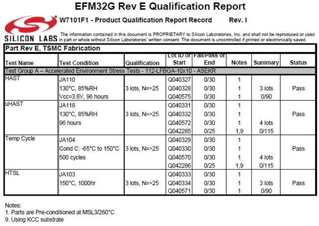
1 Change of Substrate Vendor from SEMCO to KCC PCN Issue Date: 12/20/2017 Effective Date: 3/23/2018 PCN Type: Assembly Description of Change Silicon Labs is pleased to announce a change of substrate vendor for 112-LFBGA-10x10, 120-VFBGA-7x7, 14-LGA-5x5 and 47- LGA-6x8 based on the successful qualification. There is no difference in material, design, dimension, drawing, and tolerance between SEMCO & KCC substrates. As of the effective date of the PCN, Silicon Labs will continue to fulfill orders using substrates from both SEMCO & KCC. The package qualification report is attached. Reason for Change The current substrate supplier, SEMCO, announced EOL of the substrates that are used for 112-LFBGA-10x10, 120-VFBGA- 7x7, 14-LGA-5x5 and 47-LGA-6x8 package. Impact on Form, Fit, Function, Quality, Reliability There is no impact to form, fit, function, quality or reliability of the product Product Identification Existing Part # EFM32G290F128-BGA112T EFM32G290F128-BGA112 EFM32G290F32-BGA112T EFM32G290F32-BGA112 EFM32G290F64-BGA112T EFM32G290F64-BGA112 EFM32G290F32G-E-BGA112 EFM32G290F32G-E-BGA112R EFM32G290F64G-E-BGA112 EFM32G290F64G-E-BGA112R EFM32G290F128G-E-BGA112 EFM32G290F128G-E-BGA112R EFM32G890F128-BGA112T EFM32G890F128-BGA112 EFM32G890F32-BGA112T EFM32G890F32-BGA112 EFM32G890F64-BGA112T EFM32G890F64-BGA112 EFM32G890F32G-E-BGA112 EFM32G890F32G-E-BGA112R EFM32G890F64G-E-BGA112 EFM32G890F64G-E-BGA112R EFM32G890F128G-E-BGA112 EFM32G890F128G-E-BGA112R EFM32GG290F1024-BGA112T EFM32GG290F1024-BGA112 EFM32GG290F512-BGA112T 1
2 EFM32GG290F512-BGA112 EFM32GG290F512G-E-BGA112 EFM32GG290F512G-E-BGA112R EFM32GG290F1024G-E-BGA112 EFM32GG290F1024G-E-BGA112R EFM32GG295F1024-BGA120T EFM32GG295F1024-BGA120 EFM32GG295F512-BGA120T EFM32GG295F512-BGA120 EFM32GG295F512G-E-BGA120 EFM32GG295F512G-E-BGA120R EFM32GG295F1024G-E-BGA120 EFM32GG295F1024G-E-BGA120R EFM32GG390F1024-BGA112T EFM32GG390F1024-BGA112 EFM32GG390F512-BGA112T EFM32GG390F512-BGA112 EFM32GG390F512G-E-BGA112 EFM32GG390F512G-E-BGA112R EFM32GG390F1024G-E-BGA112 EFM32GG390F1024G-E-BGA112R EFM32GG395F1024-BGA120T EFM32GG395F1024-BGA120 EFM32GG395F512-BGA120T EFM32GG395F512-BGA120 EFM32GG395F512G-E-BGA120 EFM32GG395F512G-E-BGA120R EFM32GG395F1024G-E-BGA120 EFM32GG395F1024G-E-BGA120R EFM32GG890F1024-BGA112T EFM32GG890F1024-BGA112 EFM32GG890F512-BGA112T EFM32GG890F512-BGA112 EFM32GG890F512G-E-BGA112 EFM32GG890F512G-E-BGA112R EFM32GG890F1024G-E-BGA112 EFM32GG890F1024G-E-BGA112R EFM32GG895F1024-BGA120T EFM32GG895F1024-BGA120 EFM32GG895F512-BGA120T EFM32GG895F512-BGA120 EFM32GG895F512G-E-BGA120 EFM32GG895F512G-E-BGA120R EFM32GG895F1024G-E-BGA120 EFM32GG895F1024G-E-BGA120R EFM32GG990F1024-BGA112T EFM32GG990F1024-BGA112 EFM32GG990F512-BGA112T EFM32GG990F512-BGA112 EFM32GG990F512G-E-BGA112 EFM32GG990F512G-E-BGA112R EFM32GG990F1024G-E-BGA112 EFM32GG990F1024G-E-BGA112R EFM32GG995F1024-BGA120T EFM32GG995F1024-BGA120 EFM32GG995F512-BGA120T EFM32GG995F512-BGA120 EFM32GG995F512G-E-BGA120 EFM32GG995F512G-E-BGA120R EFM32GG995F1024G-E-BGA120 EFM32GG995F1024G-E-BGA120R SI8233AB-D-IM SI8233AB-D-IMR SI8233BB-D-IM SI8233BB-D-IMR SI8233CB-D-IM SI8233CB-D-IMR Process Change Notice 2
3 SI8234AB-D-IM SI8234AB-D-IMR SI8234BB-D-IM SI8234BB-D-IMR SI8235AB-D-IM SI8235AB-D-IMR SI8235BB-AM SI8235BB-AMR SI8235BB-D-IM SI8235BB-D-IMR SI8235BB-D-YM0 SI8235BB-D-YM0R SI32260-C-FM2 SI32260-C-FM2R SI32260-C-GM2 SI32260-C-GM2R SI32260-C-ZM2 SI32260-C-ZM2R SI32261-C-FM2 SI32261-C-FM2R SI32261-C-GM2 SI32261-C-GM2R SI32261-C-ZM2 SI32261-C-ZM2R Process Change Notice Last Date of Unchanged Product: 3/23/2018 Qualification Samples Available upon request Specific conditions of acceptance of this change will be considered on a case by case basis if written notice is submitted within 30 days of this notice. To request further data or inquire about this notification, please contact your local Silicon Labs sales representative. A list of Silicon Labs sales representatives is available at In some cases rejection of a change notice may impact Silicon Labs product pricing, delivery, quality, or reliability. Customer Early Acceptance Sign Off Customers may approve early PCN acceptance by completing the information below: Early Acceptance: Date: Name: Company: your early Acceptance approval to: PCNEarlyAcceptance@silabs.com User Registration Register today to create your account on Silabs.com. Your personalized profile allows you to receive technical document updates, new product announcements, how-to and design documents, product change notices (PCN) and other valuable content available only to registered users. Qualification Data Please see below qualification reports. 3
4 4
5 5
6 6
7 7
8 8
9 9


10 Disclaimer Silicon Labs intends to provide customers with the latest, accurate, and in-depth documentation of all peripherals and modules available for system and software implementers using or intending to use the Silicon Labs products. Characterization data, available modules and peripherals, memory sizes and memory addresses refer to each specific device, and "Typical" parameters provided can and do vary in different applications. Application examples described herein are for illustrative purposes only. Silicon Labs reserves the right to make changes without further notice and limitation to product information, specifications, and descriptions herein, and does not give warranties as to the accuracy or completeness of the included information. Silicon Labs shall have no liability for the consequences of use of the information supplied herein. This document does not imply or express copyright licenses granted hereunder to design or fabricate any integrated circuits. The products are not designed or authorized to be used within any Life Support System without the specific written consent of Silicon Labs. A "Life Support System" is any product or system intended to support or sustain life and/or health, which, if it fails, can be reasonably expected to result in significant personal injury or death. Silicon Labs products are not designed or authorized for military applications. Silicon Labs products shall under no circumstances be used in weapons of mass destruction including (but not limited to) nuclear, biological or chemical weapons, or missiles capable of delivering such weapons. Trademark Information Silicon Laboratories Inc., Silicon Laboratories, Silicon Labs, SiLabs and the Silicon Labs logo, Bluegiga, Bluegiga Logo, Clockbuilder, CMEMS, DSPLL, EFM, EFM32, EFR, Ember, Energy Micro, Energy Micro logo and combinations thereof, "the world s most energy friendly microcontrollers", Ember, EZLink, EZRadio, EZRadioPRO, Gecko, ISOmodem, Micrium, Precision32, ProSLIC, Simplicity Studio, SiPHY, Telegesis, the Telegesis Logo, USBXpress, Zentri and others are trademarks or registered trademarks of Silicon Labs. ARM, CORTEX, Cortex-M3 and THUMB are trademarks or registered trademarks of ARM Holdings. Keil is a registered trademark of ARM Limited. All other products or brand names mentioned herein are trademarks of their respective holders. Silicon Laboratories Inc. 400 West Cesar Chavez Austin, TX
Si21xxx-yyy-GM SMIC 55NLL New Raw Wafer Suppliers
 180515299 Si21xxx-yyy-GM SMIC 55NLL New Raw Wafer Suppliers Issue Date: 5/15/2018 Effective Date: 5/15/2018 Description of Change Silicon Labs is pleased to announce that SMIC foundry supplier has qualified
Assembly Site Addition (UTL3)
") Process Change Notice 171117179 Assembly Site Addition (UTL3) PCN Issue Date: 11/17/2017 Effective Date: 2/22/2018 PCN Type: Assembly Description of Change Silicon Labs is pleased to announce the successful
Process Change Notice 171117179 Assembly Site Addition (UTL3) PCN Issue Date: 11/17/2017 Effective Date: 2/22/2018 PCN Type: Assembly Description of Change Silicon Labs is pleased to announce the successful
Table 1. TS1100 and MAX9634 Data Sheet Specifications. TS1100 ±30 (typ) ±100 (typ) Gain Error (%) ±0.1% ±0.1%
 ±100 (typ) Gain Error (%) ±0.1% ±0.1%") Current Sense Amplifier Performance Comparison: TS1100 vs. Maxim MAX9634 1. Introduction Overall measurement accuracy in current-sense amplifiers is a function of both gain error and amplifier input offset
Current Sense Amplifier Performance Comparison: TS1100 vs. Maxim MAX9634 1. Introduction Overall measurement accuracy in current-sense amplifiers is a function of both gain error and amplifier input offset
AN599. Si4010 ARIB STD T-93 TEST RESULTS (315 MHZ) 1. Introduction. 2. Relevant Measurements Limits DKPB434-BS Schematic and Layout
 1. Introduction. 2. Relevant Measurements Limits DKPB434-BS Schematic and Layout") Si4010 ARIB STD T-93 TEST RESULTS (315 MHZ) 1. Introduction This document provides Si4010 ARIB STD T-93 test results when operating in the 315 MHz frequency band. The results demonstrate full compliance
Si4010 ARIB STD T-93 TEST RESULTS (315 MHZ) 1. Introduction This document provides Si4010 ARIB STD T-93 test results when operating in the 315 MHz frequency band. The results demonstrate full compliance
UG175: TS331x EVB User's Guide
 UG175: TS331x EVB User's Guide The TS331x is a low power boost converter with an industry leading low quiescent current of 150 na, enabling ultra long battery life in systems running from a variety of
AN862: Optimizing Jitter Performance in Next-Generation Internet Infrastructure Systems
 AN862: Optimizing Jitter Performance in Next-Generation Internet Infrastructure Systems To realize 100 fs jitter performance of the Si534x jitter attenuators and clock generators in real-world applications,
TS1105/06/09 Current Sense Amplifier EVB User's Guide
 TS1105/06/09 Current Sense Amplifier EVB User's Guide The TS1105, TS1106, and TS1109 combine a high-side current sense amplifier (CSA) with a buffered output featuring an adjustable bias. The TS1109 bidirectional
Figure 1. Low Voltage Current Sense Amplifier Utilizing Nanopower Op-Amp and Low-Threshold P-Channel MOSFET
 SUB-1 V CURRENT SENSING WITH THE TS1001, A 0.8V, 0.6µA OP-AMP 1. Introduction AN833 Current-sense amplifiers can monitor battery or solar cell currents, and are useful to estimate power capacity and remaining
AN985: BLE112, BLE113 AND BLE121LR RANGE ANALYSIS
 AN985: BLE112, BLE113 AND BLE121LR RANGE ANALYSIS APPLICATION NOTE Thursday, 15 May 2014 Version 1.1 VERSION HISTORY Version Comment 1.0 Release 1.1 BLE121LR updated, BLE112 carrier measurement added Silicon
AN1093: Achieving Low Jitter Using an Oscillator Reference with the Si Jitter Attenuators
 AN1093: Achieving Low Jitter Using an Oscillator Reference with the Si5342-47 Jitter Attenuators This applican note references the Si5342-7 jitter attenuator products that use an oscillator as the frequency
UG123: SiOCXO1-EVB Evaluation Board User's Guide
 UG123: SiOCXO1-EVB Evaluation Board User's Guide The Silicon Labs SiOCXO1-EVB (kit) is used to help evaluate Silicon Labs Jitter Attenuator and Network Synchronization products for Stratum 3/3E, IEEE 1588
TS3003 Demo Board FEATURES COMPONENT LIST ORDERING INFORMATION. TS3003 Demo Board TS3003DB
 FEATURES 5V Supply Voltage FOUT/PWMOUT Output Period: 40µs(25kHz) o RSET = 4.32MΩ PWMOUT Output Duty Cycle: o 75% with CPWM = 100pF PWMOUT Duty Cycle Reduction o 1MΩ Potentiometer Fully Assembled and Tested
AN0026.1: EFM32 and EFR32 Wireless SOC Series 1 Low Energy Timer
 AN0026.1: EFM32 and EFR32 Wireless SOC Series 1 Low Energy Timer This application note gives an overview of the Low Energy Timer (LETIMER) and demonstrates how to use it on the EFM32 and EFR32 wireless
Normal Oscillator Behavior (Device A) Figure 1. Normal Oscillator Behavior (Device A) ft = f0 1 + TC1 T T0
 Figure 1. Normal Oscillator Behavior (Device A) ft = f0 1 + TC1 T T0") TEMPERATURE-COMPENSATED OSCILLATOR EXAMPLE 1. Introduction All Silicon Labs C8051F5xx MCU devices have an internal oscillator frequency tolerance of ±0.5%, which is rated at the oscillator s average frequency.
TEMPERATURE-COMPENSATED OSCILLATOR EXAMPLE 1. Introduction All Silicon Labs C8051F5xx MCU devices have an internal oscillator frequency tolerance of ±0.5%, which is rated at the oscillator s average frequency.
AN0026.0: EFM32 and EZR32 Wireless MCU Series 0 Low Energy Timer
 AN0026.0: EFM32 and EZR32 Wireless MCU Series 0 Low Energy Timer This application note gives an overview of the Low Energy Timer (LETIMER) and demonstrates how to use it on the EFM32 and EZR32 wireless
TS3004 Demo Board FEATURES COMPONENT LIST ORDERING INFORMATION. TS3004 Demo Board TS3004DB. 5V Supply Voltage FOUT/PWMOUT Output Period Range:
 FEATURES 5V Supply Voltage FOUT/PWMOUT Output Period Range: o 40µs tfout 1.398min o RSET = 4.32MΩ PWMOUT Output Duty Cycle: o 75% for FDIV2:0 = 000 o CPWM = 100pF PWMOUT Duty Cycle Reduction o 1MΩ Potentiometer
AN31. I NDUCTOR DESIGN FOR THE Si41XX SYNTHESIZER FAMILY. 1. Introduction. 2. Determining L EXT. 3. Implementing L EXT
 I NDUCTOR DESIGN FOR THE Si4XX SYNTHESIZER FAMILY. Introduction Silicon Laboratories family of frequency synthesizers integrates VCOs, loop filters, reference and VCO dividers, and phase detectors in standard
IN1/XA C PAR IN2/XB. Figure 1. Equivalent Crystal Circuit
 CRYSTAL SELECTION GUIDE FOR Si533X AND Si5355/56 DEVICES 1. Introduction This application note provides general guidelines for the selection and use of crystals with the Si533x and Si5355/56 family of
AN656. U SING NEC BJT(NESG AND NESG250134) POWER AMPLIFIER WITH Si446X. 1. Introduction. 2. BJT Power Amplifier (PA) and Match Circuit
 POWER AMPLIFIER WITH Si446X. 1. Introduction. 2. BJT Power Amplifier (PA) and Match Circuit") U SING NEC BJT(NESG270034 AND NESG250134) POWER AMPLIFIER WITH Si446X 1. Introduction Silicon Laboratories' Si446x devices are high-performance, low-current transceivers covering the sub-ghz frequency
U SING NEC BJT(NESG270034 AND NESG250134) POWER AMPLIFIER WITH Si446X 1. Introduction Silicon Laboratories' Si446x devices are high-performance, low-current transceivers covering the sub-ghz frequency
Si Data Short
 High-Performance Automotive AM/FM Radio Receiver and HD Radio /DAB/DAB+/DMB/DRM Tuner The Si47961/62 integrates two global radio receivers. The analog AM/FM receivers and digital radio tuners set a new
AN523. OVERLAY CONSIDERATIONS FOR THE Si114X SENSOR. 1. Introduction. 2. Typical Application
 OVERLAY CONSIDERATIONS FOR THE Si114X SENSOR 1. Introduction The Si1141/42/43 infrared proximity detector with integrated ambient light sensor (ALS) is a flexible, highperformance solution for proximity-detection
Si Data Short
 High-Performance Automotive AM/FM Radio Receiver and HD Radio /DAB/DAB+/DMB/DRM Tuner with Audio System The Si47971/72 integrates two global radio receivers with audio processing. The analog AM/FM receivers
AN959: DCO Applications with the Si5341/40
 AN959: DCO Applications with the Si5341/40 Generically speaking, a DCO is the same thing as a numerically controlled oscillator (NCO) or a direct digital synthesizer (DDS). All of these devices are oscillators
Description. Benefits. Logic Control. Rev 2.1, May 2, 2008 Page 1 of 11
 Key Features DC to 220 MHz operating frequency range Low output clock skew: 60ps-typ Low part-to-part output skew: 80 ps-typ 3.3V to 2.5V operation supply voltage range Low power dissipation: - 10 ma-typ
INPUT DIE V DDI V DD2 ISOLATION ISOLATION XMIT GND2. Si8710 Digital Isolator. Figure 1. Si8710 Digital Isolator Block Diagram
 ISOLATION ISOLATION AN729 REPLACING TRADITIONAL OPTOCOUPLERS WITH Si87XX DIGITAL ISOLATORS 1. Introduction Opto-couplers are a decades-old technology widely used for signal isolation, typically providing
Si4825-DEMO. Si4825 DEMO BOARD USER S GUIDE. 1. Features. Table 1. Si4825 Band Sequence Definition
 Si4825 DEMO BOARD USER S GUIDE 1. Features ATAD (analog tune and analog display) AM/FM/SW radio Worldwide FM band support 64 109 MHz with 18 bands, see the Table 1 Worldwide AM band support 504 1750 khz
profile for maximum EMI Si50122-A5 does not support Solid State Drives (SSD) Wireless Access Point Home Gateway Digital Video Cameras REFOUT DIFF1
 Wireless Access Point Home Gateway Digital Video Cameras REFOUT DIFF1") CRYSTAL-LESS PCI-EXPRESS GEN 1, GEN 2, & GEN 3 DUAL OUTPUT CLOCK GENERATOR Features Crystal-less clock generator with Triangular spread spectrum integrated CMEMS profile for maximum EMI PCI-Express Gen
CRYSTAL-LESS PCI-EXPRESS GEN 1, GEN 2, & GEN 3 DUAL OUTPUT CLOCK GENERATOR Features Crystal-less clock generator with Triangular spread spectrum integrated CMEMS profile for maximum EMI PCI-Express Gen
Table MHz TCXO Sources. AVX/Kyocera KT7050B KW33T
 U SING THE Si5328 IN ITU G.8262-COMPLIANT SYNCHRONOUS E THERNET APPLICATIONS 1. Introduction The Si5328 and G.8262 The Si5328 is a Synchronous Ethernet (SyncE) PLL providing any-frequency translation and
AN255. REPLACING 622 MHZ VCSO DEVICES WITH THE Si55X VCXO. 1. Introduction. 2. Modulation Bandwidth. 3. Phase Noise and Jitter
 REPLACING 622 MHZ VCSO DEVICES WITH THE Si55X VCXO 1. Introduction The Silicon Laboratories Si550 is a high-performance, voltage-controlled crystal oscillator (VCXO) device that is suitable for use in
When paired with a compliant TCXO or OCXO, the Si5328 fully meets the requirements set forth in G.8262/Y ( SyncE ), as shown in Table 1.
, as shown in Table 1.") Si5328: SYNCHRONOUS ETHERNET* COMPLIANCE TEST REPORT 1. Introduction Synchronous Ethernet (SyncE) is a key solution used to distribute Stratum 1 traceable frequency synchronization over packet networks,
Si5328: SYNCHRONOUS ETHERNET* COMPLIANCE TEST REPORT 1. Introduction Synchronous Ethernet (SyncE) is a key solution used to distribute Stratum 1 traceable frequency synchronization over packet networks,
AN933: EFR32 Minimal BOM
 The purpose of this application note is to illustrate bill-of-material (BOM)-optimized solutions for sub-ghz and 2.4 GHz applications using the EFR32 Wireless Gecko Portfolio. Silicon Labs reference radio
WT11I DESIGN GUIDE. Monday, 28 November Version 1.1
 WT11I DESIGN GUIDE Monday, 28 November 2011 Version 1.1 Contents: WT11i... 1 Design Guide... 1 1 INTRODUCTION... 5 2 TYPICAL EMC PROBLEMS WITH BLUETOOTH... 6 2.1 Radiated Emissions... 6 2.2 RF Noise in
AN1104: Making Accurate PCIe Gen 4.0 Clock Jitter Measurements
 AN1104: Making Accurate PCIe Gen 4.0 Clock Jitter Measurements The Si522xx family of clock generators and Si532xx buffers were designed to meet and exceed the requirements detailed in PCIe Gen 4.0 standards.
Figure 1. LDC Mode Operation Example
 EZRADIOPRO LOW DUTY CYCLE MODE OPERATION 1. Introduction Figure 1. LDC Mode Operation Example Low duty cycle (LDC) mode is designed to allow low average current polling operation of the Si443x RF receiver
Optocoupler 8. Shield. Optical Receiver. Figure 1. Optocoupler Block Diagram
 USING THE Si87XX FAMILY OF DIGITAL ISOLATORS 1. Introduction Optocouplers provide both galvanic signal isolation and output level shifting in a single package but are notorious for their long propagation
90 µa max supply current 9 µa shutdown current Operating Temperature Range: 40 to +85 C 5-pin SOT-23 package RoHS-compliant
 HIGH-SIDE CURRENT SENSE AMPLIFIER Features Complete, unidirectional high-side current sense capability 0.2% full-scale accuracy +5 to +36 V supply operation 85 db power supply rejection 90 µa max supply
Figure 1. Typical System Block Diagram
 Si5335 SOLVES TIMING CHALLENGES IN PCI EXPRESS, C OMPUTING, COMMUNICATIONS AND FPGA-BASED SYSTEMS 1. Introduction The Si5335 is ideally suited for PCI Express (PCIe) and FPGA-based embedded computing and
AN114. Scope. Safety. Materials H AND SOLDERING TUTORIAL FOR FINE PITCH QFP DEVICES. Optional. Required. 5. Solder flux - liquid type in dispenser
 H AND SOLDERING TUTORIAL FOR FINE PITCH QFP DEVICES Scope This document is intended to help designers create their initial prototype systems using Silicon Lab's TQFP and LQFP devices where surface mount
Low Jitter and Skew 10 to 220 MHz Zero Delay Buffer (ZDB) Description. Benefits. Low Power and Low Jitter PLL. (Divider for -2 only) GND
 Description. Benefits. Low Power and Low Jitter PLL. (Divider for -2 only) GND") Key Features 10 to 220 MHz operating frequency range Low output clock skew: 60ps-typ Low output clock Jitter: Low part-to-part output skew: 150 ps-typ 3.3V to 2.5V power supply range Low power dissipation:
Key Features 10 to 220 MHz operating frequency range Low output clock skew: 60ps-typ Low output clock Jitter: Low part-to-part output skew: 150 ps-typ 3.3V to 2.5V power supply range Low power dissipation:
AN905 EXTERNAL REFERENCES: OPTIMIZING PERFORMANCE. 1. Introduction. Figure 1. Si5342 Block Diagram. Devices include: Si534x Si5380 Si539x
 EXTERNAL REFERENCES: OPTIMIZING PERFORMANCE 1. Introduction Devices include: Si534x Si5380 Si539x The Si5341/2/4/5/6/7 and Si5380 each have XA/XB inputs, which are used to generate low-phase-noise references
BGM13P22 Module Radio Board BRD4306A Reference Manual
 BGM13P22 Module Radio Board BRD4306A Reference Manual The BRD4306A Blue Gecko Radio Board contains a Blue Gecko BGM13P22 module which integrates Silicon Labs' EFR32BG13 Blue Gecko SoC into a small form
UG310: XBee3 Expansion Kit User's Guide
 UG310: XBee3 Expansion Kit User's Guide The XBee3 Expansion Kit is an excellent way to explore and evaluate the XBee3 LTE-M cellular module which allows you to add low-power long range wireless connectivity
UG310: LTE-M Expansion Kit User's Guide
 The LTE-M Expansion Kit is an excellent way to explore and evaluate the Digi XBee3 LTE-M cellular module which allows you to add low-power long range wireless connectivity to your EFM32/EFR32 embedded
Case study for Z-Wave usage in the presence of LTE. Date CET Initials Name Justification
 Instruction LTE Case Study Document No.: INS12840 Version: 2 Description: Case study for Z-Wave usage in the presence of LTE Written By: JPI;PNI;BBR Date: 2018-03-07 Reviewed By: Restrictions: NTJ;PNI;BBR
The 500 Series Z-Wave Single Chip ADC. Date CET Initials Name Justification
 Application Note The 500 Series Z-Wave Single Chip Document No.: APL12678 Version: 2 Description: This application note describes how to use the in the 500 Series Z-Wave Single Chip Written By: OPP;MVO;BBR
TSM6025. A +2.5V, Low-Power/Low-Dropout Precision Voltage Reference FEATURES DESCRIPTION APPLICATIONS TYPICAL APPLICATION CIRCUIT
 A +2.5V, Low-Power/Low-Dropout Precision Voltage Reference FEATURES Alternate Source for MAX6025 Initial Accuracy: 0.2% (max) TSM6025A 0.4% (max) TSM6025B Temperature Coefficient: 15ppm/ C (max) TSM6025A
Description. Benefits. Low Jitter PLL With Modulation Control. Input Decoder SSEL0 SSEL1. Figure 1. Block Diagram
 Low Jitter and Power Clock Generator with SSCG Key Features Low power dissipation - 14.5mA-typ CL=15pF - 20.0mA-max CL=15pF 3.3V +/-10% power supply range 27.000MHz crystal or clock input 27.000MHz REFCLK
package and pinout temperature range Test and measurement Storage FPGA/ASIC clock generation 17 k * 3
 1 ps MAX JITTER CRYSTAL OSCILLATOR (XO) (10 MHZ TO 810 MHZ) Features Available with any-frequency output Available CMOS, LVPECL, frequencies from 10 to 810 MHz LVDS, and CML outputs 3rd generation DSPLL
AN1005: EZR32 Layout Design Guide
 The purpose of this application note is to help users design PCBs for EZR32 Wireless MCUs using best design practices that result in excellent RF performance. EZR32 wireless MCUs are based on the Si4455/Si446x
AN614 A SIMPLE ALTERNATIVE TO ANALOG ISOLATION AMPLIFIERS. 1. Introduction. Input. Output. Input. Output Amp. Amp. Modulator or Driver
 A SIMPLE ALTERNATIVE TO ANALOG ISOLATION AMPLIFIERS 1. Introduction Analog circuits sometimes require linear (analog) signal isolation for safety, signal level shifting, and/or ground loop elimination.
TSM9634F. A 1µA, SOT23 Precision Current-Sense Amplifier DESCRIPTION FEATURES APPLICATIONS TYPICAL APPLICATION CIRCUIT
 A 1µA, SOT23 Precision Current-Sense Amplifier FEATURES Second-source for MAX9634F Ultra-Low Supply Current: 1μA Wide Input Common Mode Range: +1.6V to +28V Low Input Offset Voltage: 25µV (max) Low Gain
Low-Power Single/Dual-Supply Dual Comparator with Reference. A 5V, Low-Parts-Count, High-Accuracy Window Detector
 Low-Power Single/Dual-Supply Dual Comparator with Reference FEATURES Ultra-Low Quiescent Current: 4μA (max), Both Comparators plus Reference Single or Dual Power Supplies: Single: +.5V to +11V Dual: ±1.5V
Si52111-B3/B4 PCI-EXPRESS GEN 2 SINGLE OUTPUT CLOCK GENERATOR. Features. Applications. Description. compliant. 40 to 85 C
 PCI-EXPRESS GEN 2 SINGLE OUTPUT CLOCK GENERATOR Features PCI-Express Gen 1 and Gen 2 Extended Temperature: compliant 40 to 85 C Low power HCSL differential 3.3 V Power supply output buffer Small package
Not Recommended for New Design. SL28PCIe16. EProClock PCI Express Gen 2 & Gen 3 Clock Generator. Features. Pin Configuration.
 Features SL28PCIe16 EProClock PCI Express Gen 2 & Gen 3 Clock Generator Optimized 100 MHz Operating Frequencies to Meet the Next Generation PCI-Express Gen 2 & Gen 3 Low power push-pull type differential
The Si86xxIsoLin reference design board contains three different analog isolation circuits with performance summarized in Table 1.
 Si86XX ISOLINEAR USER S GUIDE. Introduction The ISOlinear reference design modulates the incoming analog signal, transmits the resulting digital signal through the Si86xx digital isolator, and filters
UG168: Si8284-EVB User's Guide
 This document describes the operation of the Si8284-EVB. The Si8284 Evaluation Kit contains the following items: Si8284-EVB Si8284CD-IS installed on the evaluation board. KEY POINTS Discusses hardware
Features + DATAIN + REFCLK RATESEL1 CLKOUT RESET/CAL. Si DATAOUT DATAIN LOS_LVL + RATESEL1 LOL LTR SLICE_LVL RESET/CAL
 E VALUATION BOARD FOR Si5022 SiPHY MULTI-RATE SONET/SDH CLOCK AND DATA RECOVERY IC Description The Si5022 evaluation board provides a platform for testing and characterizing Silicon Laboratories Si5022
TS A 0.65V/1µA Nanopower Voltage Detector with Dual Outputs DESCRIPTION FEATURES APPLICATIONS TYPICAL APPLICATION CIRCUIT
 FEATURES Nanopower Voltage Detector in Single 4 mm 2 Package Ultra Low Total Supply Current: 1µA (max) Supply Voltage Operation: 0.65V to 2.5V Preset 0.78V UVLO Trip Threshold Internal ±10mV Hysteresis
AN427. EZRADIOPRO Si433X & Si443X RX LNA MATCHING. 1. Introduction. 2. Match Network Topology Three-Element Match Network
 EZRADIOPRO Si433X & Si443X RX LNA MATCHING 1. Introduction The purpose of this application note is to provide a description of the impedance matching of the RX differential low noise amplifier (LNA) on
Low-Power Single/Dual-Supply Quad Comparator with Reference FEATURES
 Low-Power Single/Dual-Supply Quad Comparator with Reference FEATURES Ultra-Low Quiescent Current: 5.μA (max), All comparators plus Reference Single or Dual Power Supplies: Single: +.5V to +V Dual: ±.5V
Description. Benefits. Low Jitter PLL With Modulation Control. Input Decoder SSEL0 SSEL1. Figure 1. Block Diagram. Rev 2.6, August 1, 2010 Page 1 of 9
 Key Features Low power dissipation - 13.5mA-typ CL=15pF - 18.0mA-max CL=15pF 3.3V +/-10% power supply range 27.000MHz crystal or clock input 27.000MHz REFCLK 100MHz SSCLK with SSEL0/1 spread options Low
3.2x5 mm packages. temperature range. Test and measurement Storage FPGA/ASIC clock generation. 17 k * 3
 1 ps MAX JITTER CRYSTAL OSCILLATOR (XO) (10 MHZ TO 810 MHZ) Features Available with any-frequency output Available CMOS, LVPECL, frequencies from 10 to 810 MHz LVDS, and CML outputs 3rd generation DSPLL
Si597 QUAD FREQUENCY VOLTAGE-CONTROLLED CRYSTAL OSCILLATOR (VCXO) 10 TO 810 MHZ. Features. Applications. Description. Functional Block Diagram.
 10 TO 810 MHZ. Features. Applications. Description. Functional Block Diagram.") QUAD FREQUENCY VOLTAGE-CONTROLLED CRYSTAL OSCILLATOR (VCXO) 10 TO 810 MHZ Features Available with any-frequency output from 10 to 810 MHz 4 selectable output frequencies 3rd generation DSPLL with superior
QUAD FREQUENCY VOLTAGE-CONTROLLED CRYSTAL OSCILLATOR (VCXO) 10 TO 810 MHZ Features Available with any-frequency output from 10 to 810 MHz 4 selectable output frequencies 3rd generation DSPLL with superior
Si720x Switch/Latch Hall Effect Magnetic Position Sensor Data Sheet
 Si720x Switch/Latch Hall Effect Magnetic Position Sensor Data Sheet The Si7201/2/3/4/5/6 family of Hall effect magnetic sensors and latches from Silicon Labs combines a chopper-stabilized Hall element
AN1057: Hitless Switching using Si534x/8x Devices
 AN1057: Hitless Switching using Si534x/8x Devices Hitless switching is a requirement found in many communications systems using phase and frequency synchronization. Hitless switching allows the input clocks
TS1105/06 Data Sheet. TS1105 and TS1106 Unidirectional and Bidirectional Current- Sense Amplifiers + Buffered Unipolar Output with Adjustable Bias
 TS1105 and TS1106 Unidirectional and Bidirectional Current- Sense Amplifiers + Buffered Unipolar Output with Adjustable Bias The TS1105 and TS1106 combine the TS1100 or TS1101 current-sense amplifiers
Pin Assignments VDD CLK- CLK+ (Top View)
") Ultra Low Jitter Any-Frequency XO (80 fs), 0.2 to 800 MHz The Si545 utilizes Silicon Laboratories advanced 4 th generation DSPLL technology to provide an ultra-low jitter, low phase noise clock at any
Ultra Low Jitter Any-Frequency XO (80 fs), 0.2 to 800 MHz The Si545 utilizes Silicon Laboratories advanced 4 th generation DSPLL technology to provide an ultra-low jitter, low phase noise clock at any
Si596 DUAL FREQUENCY VOLTAGE-CONTROLLED CRYSTAL OSCILLATOR (VCXO) 10 TO 810 MHZ. Features. Applications. Description. Functional Block Diagram.
 10 TO 810 MHZ. Features. Applications. Description. Functional Block Diagram.") DUAL FREQUENCY VOLTAGE-CONTROLLED CRYSTAL OSCILLATOR (VCXO) 10 TO 810 MHZ Features Available with any-rate output frequencies from 10 to 810 MHz Two selectable output frequencies 3 rd generation DSPLL
DUAL FREQUENCY VOLTAGE-CONTROLLED CRYSTAL OSCILLATOR (VCXO) 10 TO 810 MHZ Features Available with any-rate output frequencies from 10 to 810 MHz Two selectable output frequencies 3 rd generation DSPLL
S R EVISION D VOLTAGE- C ONTROLLED C RYSTAL O SCILLATOR ( V C X O ) 1 0 M H Z TO 1. 4 G H Z
 1 0 M H Z TO 1. 4 G H Z") VOLTAGE-CONTROLLED CRYSTAL OSCILLATOR (VCXO) 10 MHZ TO 1.4 GHZ Features Si550 R EVISION D Available with any frequency from 10 to 945 MHz and select frequencies to 1.4 GHz 3rd generation DSPLL with superior
VOLTAGE-CONTROLLED CRYSTAL OSCILLATOR (VCXO) 10 MHZ TO 1.4 GHZ Features Si550 R EVISION D Available with any frequency from 10 to 945 MHz and select frequencies to 1.4 GHz 3rd generation DSPLL with superior
Si3402B-EVB. N ON-ISOLATED EVALUATION BOARD FOR THE Si3402B. 1. Description. 2. Si3402B Board Interface
 N ON-ISOLATED EVALUATION BOARD FOR THE Si3402B 1. Description The Si3402B non-isolated evaluation board (Si3402B-EVB Rev 2) is a reference design for a power supply in a Power over Ethernet (PoE) Powered
Si595 R EVISION D VOLTAGE-CONTROLLED CRYSTAL OSCILLATOR (VCXO) 10 TO 810 MHZ. Features. Applications. Description. Functional Block Diagram.
 10 TO 810 MHZ. Features. Applications. Description. Functional Block Diagram.") R EVISION D VOLTAGE-CONTROLLED CRYSTAL OSCILLATOR (VCXO) 10 TO 810 MHZ Features Available with any-rate output frequencies from 10 to 810 MHz 3rd generation DSPLL with superior jitter performance Internal
R EVISION D VOLTAGE-CONTROLLED CRYSTAL OSCILLATOR (VCXO) 10 TO 810 MHZ Features Available with any-rate output frequencies from 10 to 810 MHz 3rd generation DSPLL with superior jitter performance Internal
AN0002.0: EFM32 and EZR32 Wireless MCU Series 0 Hardware Design Considerations
 AN0002.0: EFM32 and EZR32 Wireless MCU Series 0 Hardware Design Considerations This application note details hardware design considerations for EFM32 and EZR32 Wireless MCU Series 0 devices. For hardware
TS1109 Data Sheet. TS1109 Bidirectional Current-Sense Amplifier with Buffered Bipolar
 TS1109 Bidirectional Current-Sense Amplifier with Buffered Bipolar Output The TS1109 incorporates a bidirectional current-sense amplifier plus a buffered bipolar output with an adjustable bias. The internal
Si8751/52 Data Sheet. Isolated FET Driver with Pin Control or Diode Emulator Inputs
 Isolated FET Driver with Pin Control or Diode Emulator Inputs The Si875x enables new pathways to the creation of custom Solid State Relay (SSR) configurations. The Si875x integrates robust isolation technology
TS3300 FEATURES DESCRIPTION APPLICATIONS TYPICAL APPLICATION CIRCUIT VIN, VOUT, 3.5µA, High-Efficiency Boost + Output Load Switch
 FEATURES Combines Low-power Boost + Output Load Switch Boost Regulator Input Voltage: 0.6V- 3V Output Voltage: 1.8V- 3.6V Efficiency: Up to 84% No-load Input Current: 3.5µA Delivers >100mA at 1.8VBO from
Ultra Series Crystal Oscillator Si540 Data Sheet
 Ultra Series Crystal Oscillator Si540 Data Sheet Ultra Low Jitter Any-Frequency XO (125 fs), 0.2 to 1500 MHz The Si540 Ultra Series oscillator utilizes Silicon Laboratories advanced 4 th generation DSPLL
Ultra Series Crystal Oscillator Si562 Data Sheet
 Ultra Series Crystal Oscillator Si562 Data Sheet Ultra Low Jitter Quad Any-Frequency XO (90 fs), 0.2 to 3000 MHz The Si562 Ultra Series oscillator utilizes Silicon Laboratories advanced 4 th generation
Si8751/52 Data Sheet. Isolated FET Driver with Pin Control or Diode Emulator Inputs
 Isolated FET Driver with Pin Control or Diode Emulator Inputs The Si875x enables new pathways to creating custom solid state relay (SSR) configurations. Supporting customer-selected external FETs, the
TS1100. A 1µA, +2V to +27V SOT23 Precision Current-Sense Amplifier DESCRIPTION FEATURES APPLICATIONS TYPICAL APPLICATION CIRCUIT
 FEATURES Improved Electrical Performance over the MAX9938 and the MAX9634 Ultra-Low Supply Current: 1μA Wide Input Common Mode Range: +2V to +27V Low Input Offset Voltage: 1μV (max) Low Gain Error:
Si53360/61/62/65 Data Sheet
 Low-Jitter, LVCMOS Fanout Clock Buffers with up to 12 outputs and Frequency Range from dc to 200 MHz The Si53360/61/62/65 family of LVCMOS fanout buffers is ideal for clock/data distribution and redundant
Hardware Design Considerations
 the world's most energy friendly microcontrollers Hardware Design Considerations AN0002 - Application Note Introduction This application note is intended for system designers who require an overview of
Not Recommended for New Design. SL28PCIe25. EProClock PCI Express Gen 2 & Gen 3 Generator. Features. Block Diagram.
 Features SL28PCIe25 EProClock PCI Express Gen 2 & Gen 3 Generator Optimized 100 MHz Operating Frequencies to Meet the Next Generation PCI-Express Gen 2 & Gen 3 Low power push-pull type differential output
Date CET Initials Name Justification
 Application Note Antennas for Short Range Devices Document No.: APL10045 Version: 5 Description: - Written By: TJO;MVO;SDH;NTJ;BBR Date: 2018-03-05 Reviewed By: Restrictions: MVITHANAGE;PNI None Approved
ATDD (analog tune and digital display) FM/AM/SW radio Worldwide FM band support from 64 to 109 MHz with 5 default sub-bands:
 FM/AM/SW radio Worldwide FM band support from 64 to 109 MHz with 5 default sub-bands:") Si48/6 DEMO BOARD USER S GUIDE 1. Features ATDD (analog tune and digital display) FM/AM/SW radio Worldwide FM band support from 64 to 109 MHz with 5 default sub-bands: FM1 87 108 MHz (Demo Board Default)
Si48/6 DEMO BOARD USER S GUIDE 1. Features ATDD (analog tune and digital display) FM/AM/SW radio Worldwide FM band support from 64 to 109 MHz with 5 default sub-bands: FM1 87 108 MHz (Demo Board Default)
Ultra Series Crystal Oscillator Si540 Data Sheet
 Ultra Series Crystal Oscillator Si540 Data Sheet Ultra Low Jitter Any-Frequency XO (125 fs), 0.2 to 1500 MHz The Si540 Ultra Series oscillator utilizes Silicon Laboratories advanced 4 th generation DSPLL
Low Energy Timer. AN Application Note. Introduction
 ...the world's most energy friendly microcontrollers Low Energy Timer AN0026 - Application Note Introduction This application note gives an overview of the Low Energy Timer (LETIMER) and demonstrates how
Table 1. Si443x vs. Si446x DC Characteristics. Specification Si443x Si446x. Ambient Temperature 40 to 85 C 40 to 85 C
 TRANSITIONING FROM THE Si443X TO THE Si446X 1. Introduction This document provides assistance in transitioning from the Si443x to the Si446x EZRadioPRO transceivers. The Si446x radios represent the newest
Ultra Series Crystal Oscillator Si560 Data Sheet
 Ultra Series Crystal Oscillator Si560 Data Sheet Ultra Low Jitter Any-Frequency XO (90 fs), 0.2 to 3000 MHz OE/NC NC/OE GND Pin Assignments 1 2 3 6 5 4 The Si560 Ultra Series oscillator utilizes Silicon
AN0014: EFM32 Timers TIMER
 This application note gives an overview of the EFM32 TIMER module, followed by explanations on how to configure and use its primary functions which include up/down count, input capture, output compare,
1.6V Nanopower Comparators with/without Internal References
 TSM9117-TSM912 1.6V Nanopower Comparators with/without Internal References FEATURES Second-source for MAX9117-MAX912 Guaranteed to Operate Down to +1.6V Ultra-Low Supply Current 35nA - TSM9119/TSM912 6nA
Ultra Series Crystal Oscillator (VCXO) Si567 Data Sheet
 Si567 Data Sheet") Ultra Series Crystal Oscillator (VCXO) Si567 Data Sheet Ultra Low Jitter Quad Any-Frequency VCXO (100 fs), 0.2 to 3000 MHz The Si567 Ultra Series voltage-controlled crystal oscillator utilizes Silicon
Ultra Series Crystal Oscillator (VCXO) Si567 Data Sheet Ultra Low Jitter Quad Any-Frequency VCXO (100 fs), 0.2 to 3000 MHz The Si567 Ultra Series voltage-controlled crystal oscillator utilizes Silicon
ATDD (analog tune and digital display) FM/AM/SW radio Worldwide FM band support from 64 MHz to 109 MHz with 5 default sub-bands:
 FM/AM/SW radio Worldwide FM band support from 64 MHz to 109 MHz with 5 default sub-bands:") Si487 DEMO BOARD USER S GUIDE 1. Features ATDD (analog tune and digital display) FM/AM/SW radio Worldwide FM band support from 64 MHz to 109 MHz with 5 default sub-bands: FM1 87 108 MHz (Demo Board Default)
Si487 DEMO BOARD USER S GUIDE 1. Features ATDD (analog tune and digital display) FM/AM/SW radio Worldwide FM band support from 64 MHz to 109 MHz with 5 default sub-bands: FM1 87 108 MHz (Demo Board Default)
AN0016.1: Oscillator Design Considerations
 AN0016.1: Oscillator Design Considerations This application note provides an introduction to the oscillators in MCU Series 1 or Wireless SoC Series 1 devices and provides guidelines in selecting correct
Table 1. WMCU Replacement Types. Min VDD Flash Size Max TX Power
 SI100X/101X TO SI106X/108X WIRELESS MCU TRANSITION GUIDE 1. Introduction This document provides transition assistance from the Si100x/101x wireless MCU family to the Si106x/108x wireless MCU family. The
3.3 and 2.5 V supply options. Broadcast video. Switches/routers FPGA/ASIC clock generation CLK+ CLK GND
 VOLTAGE-CONTROLLED CRYSTAL OSCILLATOR (VCXO) 100 khz TO 250 MHZ Features Supports any frequency from Optional integrated 1:2 CMOS 100 khz to 250 MHz fanout buffer Low-jitter operation 3.3 and 2.5 V supply
EFR32MG GHz 10 dbm Radio Board BRD4162A Reference Manual
 EFR32MG12 2.4 GHz 10 dbm Radio Board BRD4162A Reference Manual The BRD4162A Mighty Gecko Radio Board enables developers to develop Zigbee, Thread, Bluetooth low energy and proprietary wireless wireless
Si510/511. CRYSTAL OSCILLATOR (XO) 100 khz TO 250 MHZ. Features. Applications. Description. Si5602. Ordering Information: See page 14.
 100 khz TO 250 MHZ. Features. Applications. Description. Si5602. Ordering Information: See page 14.") CRYSTAL OSCILLATOR (XO) 100 khz TO 250 MHZ Features Supports any frequency from 100 khz to 250 MHz Low jitter operation 2 to 4 week lead times Total stability includes 10-year aging Comprehensive production
CRYSTAL OSCILLATOR (XO) 100 khz TO 250 MHZ Features Supports any frequency from 100 khz to 250 MHz Low jitter operation 2 to 4 week lead times Total stability includes 10-year aging Comprehensive production
EFR32MG 2.4 GHz 19.5 dbm Radio Board BRD4151A Reference Manual
 EFR32MG 2.4 GHz 19.5 dbm Radio Board BRD4151A Reference Manual The EFR32MG family of Wireless SoCs deliver a high performance, low energy wireless solution integrated into a small form factor package.
AN973: Design Guide for Si8281/83 Isolated DC-DC with Internal Switch
 AN973: Design Guide for Si8281/83 Isolated DC-DC with Internal Switch The Si8281 and Si8283 products have an integrated isolated gate driver with an isolated dc-dc controller. The controller s internal
TS V Nanopower Comparator with Internal Reference DESCRIPTION FEATURES APPLICATIONS TYPICAL APPLICATION CIRCUIT
 FEATURES Improved Electrical Performance over MAX9117-MAX9118 Guaranteed to Operate Down to +1.6V Ultra-Low Supply Current: 6nA Internal 1.252V ±1% Reference Input Voltage Range Extends 2mV Outsidethe-Rails