Power Devices Prof. Dr. Ing. Hans Georg Herzog Prof. Dr. Ing. Ralph Kennel
|
|
|
- Horace Evans
- 5 years ago
- Views:
Transcription
1 Power Devices Prof. Dr. Ing. Hans Georg Herzog Prof. Dr. Ing. Ralph Kennel Technische Universität München Arcisstraße München Germany 1
2 Power Devices in power electronics active operation of power semiconductor devices is avoided either the voltage at the device is 0 or the current in the device is 0 unfortunately power semiconductor devices are no ideal switches! what requirements have to be postulated? switch off switching event switch on low blocking current low switching losses low voltage drop bidirectional blocking short switching time bidirectional conduction high blocking voltage free control of time of switching high current capability high du/dt no snubber circuits high di/dt 2
3 Losses in Real Power Semiconductor Devices switch-on losses conduction losses switch-off losses 3
 necessary low switching frequency problematic with respect to high power")
4 Hard Switching Devices high stress on semiconductor wide SOA (safe operation area) necessary low switching frequency problematic with respect to high power 4
5 Soft Switching Devices low stress on semiconductor high switch-off current possible high switching frequency simple gate driving circuits additional power components necessary 5
6 IGBT Turn-Off with Snubber hard switching with snubber Gate voltage Gate voltage Collector voltage Collector current Collector voltage E off = 226µJ E off = 98µJ Collector current 400V, 20A, 125 C, R G = 9.1Ω current pops up but losses are still greatly reduced in the semiconductor the overall losses, however, increase 6
7 Power Devices Diode (Thyristor, GTO, IGCT) Referents: Prof. Dr. Ing. Hans Georg Herzog Prof. Dr. Ing. Ralph Kennel Technische Universität München Arcisstraße München Germany 7
8 Power Diode Characteristic 8
9 Power Diode Switching-Off Behaviour 9
10 PIN - Diode to ensure a sufficient voltage capability the junction area is increased in distance p i n by introducing a so-called intrinsisc layer (= semiconductor material without any doping) between the p-doped and the n-doped layer PIN - Diode 10
11 Thyristor Structure A C A A 11
12 Thyristor Characteristic 12
13 Triac 13

14 / GTO standard thyristor technology single wafer until 150 mm low conduction losses high current capability high switching losses high power for driver circuit 14
15 GTO IGCT both are controllable thyristors however, according to different philosophies GTO earlier in the market switch-off concept : by deviating a part of the load current (ca. 30 %) via the gate filigrane structure on the chip IGCT (too) late in the market switch-off concept : by deviating the full load current via the gate very complex driver circuits 15
16 Power Devices (bipolar) Transistor Referents: Prof. Dr. Ing. Hans Georg Herzog Prof. Dr. Ing. Ralph Kennel Technische Universität München Arcisstraße München Germany 16
17 Bipolar Power Transistor 17
18 Switch-On Behaviour of a Bipolar Power Transistors 18
19 Switch-Off Behaviour of a Bipolar Power Transistors 19
20 Darlington Structure transistor in saturation U CE1 < U BE1 U BE1 = 0,7 V U BE2 = 0,7 V U CE1 = 0,3 V U CE2 = 0,7 V + 0,3 V = 1,0 V transistor achieve saturation U CE2 >> U BE2 very high conduction losses 20
21 Power Devices Field Effect Transistor (FET) Referents: Prof. Dr. Ing. Hans Georg Herzog Prof. Dr. Ing. Ralph Kennel Technische Universität München Arcisstraße München Germany 21
22 Field Effect Transistor (MOSFET) Structure channel : long and thin high internal resistance 22
23 Field Effect Transistor (MOSFET) Structure channel : still thin - but not as long any more low internal resístance 23
24 Field Effect Transistor (MOSFET) parasitic npn-transistor 24
25 Field Effect Transistor (MOSFET) parasitic capacitances 25
26 Power Devices Insulated Gate Bipolar Transistor (IGBT) Referents: Prof. Dr. Ing. Hans Georg Herzog Prof. Dr. Ing. Ralph Kennel Technische Universität München Arcisstraße München Germany 26
")
27 Insulated Gate Bipolar Transistor (IGBT) Structure 27
28 Insulated Gate Bipolar Transistor (IGBT) Structure and Equivalent Circuit bipolar pnp-transistor Think of it as a MOSFET with low conduction loss. 28
 parasitic")
29 Insulated Gate Bipolar Transistor (IGBT) parasitic capacitances 29
30 Insulated Gate Bipolar Transistor (IGBT) parasitic (latch-up) transistor this is a parasitic thyristor!! 30

31 MOSFET technology chip size until 20 x 20 mm² low power for driver circuit low switching losses high voltage drop contacting problems 31
32 On-State Voltage Comparison Same Die Size On-State Voltage vs. Current APT6038BLL: I D = 17A APT30GP60B: I C2 = 49A APT6038BLL (25 C) APT6038BLL (125 C) APT30GP60B (25 or 125 C) Voltage (V) Current (A) MOSFET 125 C MOSFET 25 C IGBT IGBT has lower on-voltage above about 4 Amps. MOSFET conduction loss is sensitive to temperature, the IGBT is not. TECHNOLOGY TO THE NEXT POWER 32
33 Conduction Loss Comparison Same Die Size Conduction Loss vs. Current (125 C) APT6038BLL APT30GP60B Power (W) MOSFET IGBT Current (A) IGBT has much lower conduction loss above about 4 Amps. IGBT has much better overload capability. TECHNOLOGY TO THE NEXT POWER 33

34 Switching Loss: 54A MOSFET vs. 72A IGBT Power MOS 7 MOSFET Power MOS 7 IGBT V GS V GS E off = 1062 µj E off = 1058 µj Current Voltage Current Voltage Tail current APT6010B2LL, 400V, 50A, 125 ºC, 5 Ohms APT50GP60B, 400V, 50A, 125 ºC, 5 Ohms At 50A, the IGBT has lower conduction loss and lower switching loss. At less current, the MOSFET would have lower E off (no tail current). The IGBT is about half the size of the MOSFET lower cost. 34 TECHNOLOGY TO THE NEXT POWER 34
35 Application Comparison Hard Switched Boost Frequency (khz) Frequency vs. Current APT15GP60B APT6029BLL MOSFET IGBT Boost: Hard switched 400V, T J = 125 C, T C = 75 C, 5 APT15GP60: I C2 = 30A APT6029: I D = 21A MOSFET is 2.5 times larger than IGBT. IGBT has good overload capability Current (Amps) MOSFET is best at low current, very high frequency. IGBT is best at high current. IGBT is lower cost. TECHNOLOGY TO THE NEXT POWER 35
36 Advantage of IGBTs Lower cost much smaller die size for same power. Excellent overload capability linear conduction loss versus current, very insensitive to temperature. Simple gate drive can replace MOSFETs positive only gate drive Highest speed IGBTs turn-on is the same as a MOSFET, turn-off is only slightly longer. Suitable for soft and hard switching zero voltage or reduced voltage turn-off not as good as MOSFETs. TECHNOLOGY TO THE NEXT POWER 36
37 Parallel Connection of IGBTs additional resistors in series semiconductor design with integrated path with a positive temperature coefficient 37
38 38
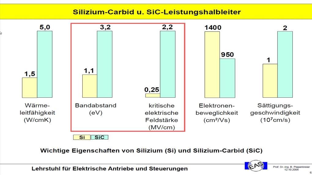
39 Siliziumkarbid (SiC) 39

40 Reasons for Wide Band Gap Devices Added Value and Related Impact source : Pierric Gueguen, Market & Technology Overview of Power Electronics Industry and Impact of WBG Devices, Yole Développement, SEMICON Europa 2014, Grenoble,

41 Quelle : Teresa Bertelshofer; Universität Erlangen 41
42 Quelle : Teresa Bertelshofer; Universität Erlangen 42

43 Quelle : Teresa Bertelshofer; Universität Erlangen 43

44 Quelle : Teresa Bertelshofer; Universität Erlangen 44
45 Quelle : Teresa Bertelshofer; Universität Erlangen 45

46 Quelle : Teresa Bertelshofer; Universität Erlangen 46

47 Quelle : Teresa Bertelshofer; Universität Erlangen 47
48 Comparison Si SiC (switching) losses source : Power Electronics Europe ; Issue Efficiency Improvement with Silicon Carbide Based 48Power Modules

49 Quelle : Teresa Bertelshofer; Universität Erlangen 49

50 Quelle : Teresa Bertelshofer; Universität Erlangen 50

51 SiC Device Application Roadmap source : Pierric Gueguen, Market & Technology Overview of Power Electronics Industry and Impact of WBG Devices, Yole Développement, SEMICON Europa 2014, Grenoble,
52 52
53 Silicon Carbide (SiC) better (faster?) switching higher temperature robustness voltage drops? cannot be produced on outsourced production lines for memory chips investment cost not negligible 53
54 Key Characteristics of GaN vs. SiC vs. Si source : ECPE 54
55 Thank You!!! Any Questions? Prof. Dr.-Ing. Ralph Kennel Technische Universität München Electrical Drive Systems and Power Electronics 55
Voltage Source Inverter (VSI)
") Voltage Source Inverter (VSI) Prof. Dr. Ing. Hans Georg Herzog (hg.herzog@tum.de) Prof. Dr. Ing. Ralph Kennel (ralph.kennel@tum.de) Technische Universität München Arcisstraße 21 80333 München Germany 1
Voltage Source Inverter (VSI) Prof. Dr. Ing. Hans Georg Herzog (hg.herzog@tum.de) Prof. Dr. Ing. Ralph Kennel (ralph.kennel@tum.de) Technische Universität München Arcisstraße 21 80333 München Germany 1
Power Semiconductor Devices
 TRADEMARK OF INNOVATION Power Semiconductor Devices Introduction This technical article is dedicated to the review of the following power electronics devices which act as solid-state switches in the circuits.
Lecture 23 Review of Emerging and Traditional Solid State Switches
 Lecture 23 Review of Emerging and Traditional Solid State Switches 1 A. Solid State Switches 1. Circuit conditions and circuit controlled switches A. Silicon Diode B. Silicon Carbide Diodes 2. Control
Exercise 6-2. The IGBT EXERCISE OBJECTIVES
 Exercise 6-2 The IGBT EXERCISE OBJECTIVES At the completion of this exercise, you will know the behaviour of the IGBT during switching operation. You will be able to explain how IGBT switching can be improved.
Power Electronics Power semiconductor devices. Dr. Firas Obeidat
 Power Electronics Power semiconductor devices Dr. Firas Obeidat 1 Table of contents 1 Introduction 2 Classifications of Power Switches 3 Power Diodes 4 Thyristors (SCRs) 5 The Triac 6 The Gate Turn-Off
Today s subject MOSFET and IGBT
 Today s subject MOSFET and IGBT 2018-05-22 MOSFET metal oxide semiconductor field effect transistor Drain Gate n-channel Source p-channel The MOSFET - Source Gate G D n + p p n + S body body n - drift
Analog and Telecommunication Electronics
 Politecnico di Torino - ICT School Analog and Telecommunication Electronics F2 Active power devices»mos»bjt» IGBT, TRIAC» Safe Operating Area» Thermal analysis 30/05/2012-1 ATLCE - F2-2011 DDC Lesson F2:
Lecture 3: Transistors
 Lecture 3: Transistors Now that we know about diodes, let s put two of them together, as follows: collector base emitter n p n moderately doped lightly doped, and very thin heavily doped At first glance,
2 Marks - Question Bank. Unit 1- INTRODUCTION
 Two marks 1. What is power electronics? EE6503 POWER ELECTRONICS 2 Marks - Question Bank Unit 1- INTRODUCTION Power electronics is a subject that concerns the applications electronics principles into situations
SiC Transistor Basics: FAQs
 SiC Transistor Basics: FAQs Silicon Carbide (SiC) MOSFETs exhibit higher blocking voltage, lower on state resistance and higher thermal conductivity than their silicon counterparts. Oct. 9, 2013 Sam Davis
Transistor Characteristics
 Transistor Characteristics Topics covered in this presentation: Transistor Construction Transistor Operation Transistor Characteristics 1 of 15 The Transistor The transistor is a semiconductor device that
Interactions Between Electrical Machine and Power Electronics
 Interactions Between Electrical Machine and Power Electronics Prof. Dr. Ing. Ralph Kennel (ralph.kennel@tum.de) Technische Universität München Arcisstraße 21 80333 München Additional Losses Prof. Dr. Ing.
TRANSISTOR TRANSISTOR
 It is made up of semiconductor material such as Si and Ge. Usually, it comprises of three terminals namely, base, emitter and collector for providing connection to the external circuit. Today, some transistors
COLLECTOR DRAIN BASE GATE EMITTER. Applying a voltage to the Gate connection allows current to flow between the Drain and Source connections.
 MOSFETS Although the base current in a transistor is usually small (< 0.1 ma), some input devices (e.g. a crystal microphone) may be limited in their output. In order to overcome this, a Field Effect Transistor
Power Electronics. P. T. Krein
 Power Electronics Day 10 Power Semiconductor Devices P. T. Krein Department of Electrical and Computer Engineering University of Illinois at Urbana-Champaign 2011 Philip T. Krein. All rights reserved.
Other Electronic Devices
 Other Electronic Devices 1 Contents Field-Effect Transistors(FETs) - JFETs - MOSFETs Insulate Gate Bipolar Transistors(IGBTs) H-bridge driver and PWM Silicon-Controlled Rectifiers(SCRs) TRIACs Device Selection
Multi-Level Inverters
 Lecture Power Electronics Multi-Level Inverters Prof. Dr. Ing. Ralph Kennel (ralph.kennel@tum.de) Technische Universität München Electrical Drive Systems and Power Electronics Arcisstraße 21 80333 München
Multi-Level Inverters
 Lecture Power Electronics Multi-Level Inverters Prof. Dr. Ing. Ralph Kennel (ralph.kennel@tum.de) Technische Universität München Arcisstraße 21 80333 München Germany MULTILEVEL INVERTERS more than 2 voltage
Prof. Steven S. Saliterman Introductory Medical Device Prototyping
 Introductory Medical Device Prototyping Department of Biomedical Engineering, University of Minnesota http://saliterman.umn.edu/ Solid state power switching: Silicon controlled rectifiers (SCR or Thyristor).
Integrated diodes. The forward voltage drop only slightly depends on the forward current. ELEKTRONIKOS ĮTAISAI
 1 Integrated diodes pn junctions of transistor structures can be used as integrated diodes. The choice of the junction is limited by the considerations of switching speed and breakdown voltage. The forward
3. Draw the two transistor model of a SCR and mention its applications. (MAY 2016)
") DHANALAKSHMI COLLEGE OF ENGINEERING DEPARTMENT OF ELECTRICAL AND ELECTRONICS ENGINEERING EE6503 POWER ELECTRONICS UNIT I- POWER SEMI-CONDUCTOR DEVICES PART - A 1. What is a SCR? A silicon-controlled rectifier
DHANALAKSHMI COLLEGE OF ENGINEERING DEPARTMENT OF ELECTRICAL AND ELECTRONICS ENGINEERING EE6503 POWER ELECTRONICS UNIT I- POWER SEMI-CONDUCTOR DEVICES PART - A 1. What is a SCR? A silicon-controlled rectifier
Power Semiconductor Devices - Silicon vs. New Materials. Si Power Devices The Dominant Solution Today
 Power Semiconductor Devices - Silicon vs. New Materials Jim Plummer Stanford University IEEE Compel Conference July 10, 2017 Market Opportunities for Power Devices Materials Advantages of SiC and GaN vs.
Field Effect Transistors
 Field Effect Transistors Purpose In this experiment we introduce field effect transistors (FETs). We will measure the output characteristics of a FET, and then construct a common-source amplifier stage,
Chapter 1 Power Electronic Devices
 Chapter 1 Power Electronic Devices Outline 1.1 An introductory overview of power electronic devices 1.2 Uncontrolled device power diode 1.3 Half- controlled device thyristor 1.4 Typical fully- controlled
ME 4447 / 6405 Student Lecture. Transistors. Abiodun Otolorin Michael Abraham Waqas Majeed
 ME 4447 / 6405 Student Lecture Transistors Abiodun Otolorin Michael Abraham Waqas Majeed Lecture Overview Transistor? History Underlying Science Properties Types of transistors Bipolar Junction Transistors
Wide Band-Gap Power Device
 Wide Band-Gap Power Device 1 Contents Revisit silicon power MOSFETs Silicon limitation Silicon solution Wide Band-Gap material Characteristic of SiC Power Device Characteristic of GaN Power Device 2 1
SRM INSTITUTE OF SCIENCE AND TECHNOLOGY (DEEMED UNIVERSITY)
") SRM INSTITUTE OF SCIENCE AND TECHNOLOGY (DEEMED UNIVERSITY) QUESTION BANK I YEAR B.Tech (II Semester) ELECTRONIC DEVICES (COMMON FOR EC102, EE104, IC108, BM106) UNIT-I PART-A 1. What are intrinsic and
SRM INSTITUTE OF SCIENCE AND TECHNOLOGY (DEEMED UNIVERSITY) QUESTION BANK I YEAR B.Tech (II Semester) ELECTRONIC DEVICES (COMMON FOR EC102, EE104, IC108, BM106) UNIT-I PART-A 1. What are intrinsic and
Introduction. Figure 2: The HiPak standard (left) and high-insulation (right) modules with 3300V SPT + IGBT technology.
 and high-insulation (right) modules with 3300V SPT + IGBT technology.") M. Rahimo, U. Schlapbach, A. Kopta, R. Schnell, S. Linder ABB Switzerland Ltd, Semiconductors, Fabrikstrasse 3, CH 5600 Lenzburg, Switzerland email: munaf.rahimo@ch.abb.com Abstract: Following the successful
M. Rahimo, U. Schlapbach, A. Kopta, R. Schnell, S. Linder ABB Switzerland Ltd, Semiconductors, Fabrikstrasse 3, CH 5600 Lenzburg, Switzerland email: munaf.rahimo@ch.abb.com Abstract: Following the successful
(a) All-SiC 2-in-1 module
 All-SiC 2-in-1 module") All-SiC -in- Module CHONABAYASHI, Mikiya * OTOMO, Yoshinori * KARASAWA, Tatsuya * A B S T R A C T Fuji Electric has developed an utilizing a SiC device that has been adopted in the development of a high-performance
All-SiC -in- Module CHONABAYASHI, Mikiya * OTOMO, Yoshinori * KARASAWA, Tatsuya * A B S T R A C T Fuji Electric has developed an utilizing a SiC device that has been adopted in the development of a high-performance
Chapter 3-2 Semiconductor devices Transistors and Amplifiers-BJT Department of Mechanical Engineering
 MEMS1082 Chapter 3-2 Semiconductor devices Transistors and Amplifiers-BJT Bipolar Transistor Construction npn BJT Transistor Structure npn BJT I = I + E C I B V V BE CE = V = V B C V V E E Base-to-emitter
Vector Control (Field Oriented Control, Direct Torque Control)
") Vector Control (Field Oriented Control, Direct Torque Control) Referents: Prof. Dr. Ing. Ralph Kennel (ralph.kennel@tum.de) Technische Universität München Arcisstraße 21 80333 München Germany 1 The General
Vector Control (Field Oriented Control, Direct Torque Control) Referents: Prof. Dr. Ing. Ralph Kennel (ralph.kennel@tum.de) Technische Universität München Arcisstraße 21 80333 München Germany 1 The General
(anode) (also: I D, I F, I T )
 (also: I D, I F, I T )") (anode) V R - V A or V D or VF or V T IA (also: I D, I F, I T ) control terminals (e.g. gate for thyrisr; basis for BJT) - (IR =-I A ) (cathode) I A I F conducting range A p n K (a) V A (V F ) - A anode
(anode) V R - V A or V D or VF or V T IA (also: I D, I F, I T ) control terminals (e.g. gate for thyrisr; basis for BJT) - (IR =-I A ) (cathode) I A I F conducting range A p n K (a) V A (V F ) - A anode
Lecture 19 Real Semiconductor Switches and the Evolution of Power MOSFETS A.. Real Switches: I(D) through the switch and V(D) across the switch
 through the switch and V(D) across the switch") Lecture 19 Real Semiconductor Switches and the Evolution of Power MOSFETS 1 A.. Real Switches: I(D) through the switch and V(D) across the switch 1. Two quadrant switch implementation and device choice
Lecture 19 Real Semiconductor Switches and the Evolution of Power MOSFETS 1 A.. Real Switches: I(D) through the switch and V(D) across the switch 1. Two quadrant switch implementation and device choice
Power Devices and Circuits
 COURSE ON Power Devices and Circuits Master degree Electronic Curriculum Teacher: Prof. Dept. of Electronics and Telecommunication Eng. University of Napoli Federico II What is the scope of Power Electronics?
4.2.2 Metal Oxide Semiconductor Field Effect Transistor (MOSFET)
") 4.2.2 Metal Oxide Semiconductor Field Effect Transistor (MOSFET) The Metal Oxide Semitonductor Field Effect Transistor (MOSFET) has two modes of operation, the depletion mode, and the enhancement mode.
4.2.2 Metal Oxide Semiconductor Field Effect Transistor (MOSFET) The Metal Oxide Semitonductor Field Effect Transistor (MOSFET) has two modes of operation, the depletion mode, and the enhancement mode.
EEL 5245 POWER ELECTRONICS I Lecture #4: Chapter 2 Switching Concepts and Semiconductor Overview
 EEL 5245 POWER ELECTRONICS I Lecture #4: Chapter 2 Switching Concepts and Semiconductor Overview Objectives of Lecture Switch realizations Objective is to focus on terminal characteristics Blocking capability
Analysis on IGBT Developments
 Analysis on IGBT Developments Mahato G.C., Niranjan and Waquar Aarif Abu RVS College of Engineering and Technology, Jamshedpur India Abstract Silicon based high power devices continue to play an important
Lecture Notes. Emerging Devices. William P. Robbins Professor, Dept. of Electrical and Computer Engineering University of Minnesota.
 Lecture Notes Emerging Devices William P. Robbins Professor, Dept. of Electrical and Computer Engineering University of Minnesota Outline Power JFET Devices Field-Controlled Thyristor MOS-Controlled Thyristor
Solid State Devices- Part- II. Module- IV
 Solid State Devices- Part- II Module- IV MOS Capacitor Two terminal MOS device MOS = Metal- Oxide- Semiconductor MOS capacitor - the heart of the MOSFET The MOS capacitor is used to induce charge at the
USING F-SERIES IGBT MODULES
 .0 Introduction Mitsubishi s new F-series IGBTs represent a significant advance over previous IGBT generations in terms of total power losses. The device remains fundamentally the same as a conventional
EXPERIMENT 5 CURRENT AND VOLTAGE CHARACTERISTICS OF BJT
 EXPERIMENT 5 CURRENT AND VOLTAGE CHARACTERISTICS OF BJT 1. OBJECTIVES 1.1 To practice how to test NPN and PNP transistors using multimeter. 1.2 To demonstrate the relationship between collector current
The two-in-one chip. The bimode insulated-gate transistor (BIGT)
") The two-in-one chip The bimode insulated-gate transistor (BIGT) Munaf Rahimo, Liutauras Storasta, Chiara Corvasce, Arnost Kopta Power semiconductor devices employed in voltage source converter (VSC) applications
The two-in-one chip The bimode insulated-gate transistor (BIGT) Munaf Rahimo, Liutauras Storasta, Chiara Corvasce, Arnost Kopta Power semiconductor devices employed in voltage source converter (VSC) applications
AE53/AC53/AT53/AE103 ELECT. DEVICES & CIRCUITS DEC 2015
 Q.2 a. By using Norton s theorem, find the current in the load resistor R L for the circuit shown in Fig.1. (8) Fig.1 IETE 1 b. Explain Z parameters and also draw an equivalent circuit of the Z parameter
UNIT I POWER SEMI-CONDUCTOR DEVICES
 UNIT I POWER SEMI-CONDUCTOR DEVICES SUBJECT CODE SUBJECT NAME STAFF NAME : EE6503 : Power Electronics : Ms.M.Uma Maheswari 1 SEMICONDUCTOR DEVICES POWER DIODE POWER TRANSISTORS POWER BJT POWER MOSFET IGBT
DHANALAKSHMI COLLEGE OF ENGINEERING DEPARTMENT OF ELECTRICAL AND ELECTRONICS ENGINEERING
 DHANALAKSHMI COLLEGE OF ENGINEERING DEPARTMENT OF ELECTRICAL AND ELECTRONICS ENGINEERING Power Diode EE2301 POWER ELECTRONICS UNIT I POWER SEMICONDUCTOR DEVICES PART A 1. What is meant by fast recovery
1 FUNDAMENTAL CONCEPTS What is Noise Coupling 1
 Contents 1 FUNDAMENTAL CONCEPTS 1 1.1 What is Noise Coupling 1 1.2 Resistance 3 1.2.1 Resistivity and Resistance 3 1.2.2 Wire Resistance 4 1.2.3 Sheet Resistance 5 1.2.4 Skin Effect 6 1.2.5 Resistance
Power Devices and ICs Chapter 15
 Power Devices and ICs Chapter 15 Syed Asad Alam DA, ISY 4/28/2015 1 Overview 4/28/2015 2 Overview Types of Power Devices PNPN Thyristor TRIAC (Triode Alternating Current) GTO (Gate Turn-Off Thyristor)
POWER ELECTRONICS. Converters, Applications, and Design. NED MOHAN Department of Electrical Engineering University of Minnesota Minneapolis, Minnesota
 POWER ELECTRONICS Converters, Applications, and Design THIRD EDITION NED MOHAN Department of Electrical Engineering University of Minnesota Minneapolis, Minnesota TORE M. UNDELAND Department of Electrical
CHAPTER I INTRODUCTION
 CHAPTER I INTRODUCTION High performance semiconductor devices with better voltage and current handling capability are required in different fields like power electronics, computer and automation. Since
M328 version ESR inductance capacitance meter multifunctional tester DIY
 M328 version ESR inductance capacitance meter multifunctional tester DIY About transistor Multifunction Tester: The tester uses 3.7V rechargeable lithium battery (battery model: 14500) powered portable
ELEC-E8421 Components of Power Electronics
 ELEC-E8421 Components of Power Electronics MOSFET 2015-10-04 Metal-Oxide-Semiconductor Field-Effect-Transistor (MOSFET) Vertical structure makes paralleling of many small MOSFETs on the chip easy. Very
Talk1: Overview of Power Devices and Technology Trends. Talk 2: Devices and Technologies for HVIC
 Talk1: Overview of Power Devices and Technology Trends Talk 2: Devices and Technologies for HVIC Prof. Florin Udrea Cambridge University Taiwan, January 2010 1 Outline Talk 1: Overview of Power Devices
Chapter 8: Field Effect Transistors
 Chapter 8: Field Effect Transistors Transistors are different from the basic electronic elements in that they have three terminals. Consequently, we need more parameters to describe their behavior than
PCB layout guidelines. From the IGBT team at IR September 2012
 PCB layout guidelines From the IGBT team at IR September 2012 1 PCB layout and parasitics Parasitics (unwanted L, R, C) have much influence on switching waveforms and losses. The IGBT itself has its own
Transistor electronic technologies
 Transistor electronic technologies Bipolar Junction Transistor discrete or integrated circuit discrete = individual component MOS (Metal-Oxide-Silicon) Field Effect Transistor mainly used in integrated
Fundamentals of Power Semiconductor Devices
 В. Jayant Baliga Fundamentals of Power Semiconductor Devices 4y Spri ringer Contents Preface vii Chapter 1 Introduction 1 1.1 Ideal and Typical Power Switching Waveforms 3 1.2 Ideal and Typical Power Device
POWER ELECTRONICS. Alpha. Science International Ltd. S.C. Tripathy. Oxford, U.K.
 POWER ELECTRONICS S.C. Tripathy Alpha Science International Ltd. Oxford, U.K. Contents Preface vii 1. SEMICONDUCTOR DIODE THEORY 1.1 1.1 Introduction 1.1 1.2 Charge Densities in a Doped Semiconductor 1.1
INTRODUCTION TO MOS TECHNOLOGY
 INTRODUCTION TO MOS TECHNOLOGY 1. The MOS transistor The most basic element in the design of a large scale integrated circuit is the transistor. For the processes we will discuss, the type of transistor
Power Semiconductor Devices for Variable Frequency Drives
 B. Jayant Baliga Chapter 1 Power Semiconductor Devices for Variable Frequency Drives 1.1. INTRODUCTION Improvements in the performance of variable frequency drives have been directly related to the availability
Modern Power Electronics Courses at UCF
 Modern Power Electronics Courses at UCF Issa Batarseh, John Shen, and Sam Abdel-Rahman School of Electrical Engineering and Computer Science University of Central Florida Orlando, Florida, USA University
4 Transistors. 4.1 IV Relations
 4 Transistors Due date: Sunday, September 19 (midnight) Reading (Bipolar transistors): HH sections 2.01-2.07, (pgs. 62 77) Reading (Field effect transistors) : HH sections 3.01-3.03, 3.11-3.12 (pgs. 113
Sonoma State University Department of Engineering Science Fall 2017
 ES-110 Laboratory Introduction to Engineering & Laboratory Experience Saeid Rahimi, Ph.D. Lab 7 Introduction to Transistors Introduction As we mentioned before, diodes have many applications which are
Power semiconductors. José M. Cámara V 1.0
 Power semiconductors José M. Cámara V 1.0 Introduction Here we are going to study semiconductor devices used in power electronics. They work under medium and high currents and voltages. Some of them only
Questions on JFET: 1) Which of the following component is a unipolar device?
 Which of the following component is a unipolar device?") Questions on JFET: 1) Which of the following component is a unipolar device? a) BJT b) FET c) DJT d) EFT 2) Current Conduction in FET takes place due e) Majority charge carriers only f) Minority charge
Questions on JFET: 1) Which of the following component is a unipolar device? a) BJT b) FET c) DJT d) EFT 2) Current Conduction in FET takes place due e) Majority charge carriers only f) Minority charge
IGBT Technologies and Applications Overview: How and When to Use an IGBT Vittorio Crisafulli, Apps Eng Manager. Public Information
 IGBT Technologies and Applications Overview: How and When to Use an IGBT Vittorio Crisafulli, Apps Eng Manager Agenda Introduction Semiconductor Technology Overview Applications Overview: Welding Induction
Semiconductor analyser AS4002P User Manual
 Semiconductor analyser AS4002P User Manual Copyright Ormelabs (C) 2010 http://www.ormelabs.com 1 CONTENTS SECTION Page SECTION 1: Introduction... 3 SECTION 2: Features... 3 SECTION 3: Component analysis...
A 6.5kV IGBT Module with very high Safe Operating Area
 A 6.5kV IGBT Module with very high Safe Operating Area A. Kopta, M. Rahimo, U. Schlapbach, D. Schneider, Eric Carroll, S. Linder IAS, October 2005, Hong Kong, China Copyright [2005] IEEE. Reprinted from
Student Lecture by: Giangiacomo Groppi Joel Cassell Pierre Berthelot September 28 th 2004
 Student Lecture by: Giangiacomo Groppi Joel Cassell Pierre Berthelot September 28 th 2004 Lecture outline Historical introduction Semiconductor devices overview Bipolar Junction Transistor (BJT) Field
IGBTs (Insulated Gate Bipolar Transistor)
") IGBTs (Insulated Gate Bipolar Transistor) Description This document describes the basic structures, ratings, and electrical characteristics of IGBTs. It also provides usage considerations for IGBTs. 1
IGBTs (Insulated Gate Bipolar Transistor) Description This document describes the basic structures, ratings, and electrical characteristics of IGBTs. It also provides usage considerations for IGBTs. 1
BJT Amplifier. Superposition principle (linear amplifier)
") BJT Amplifier Two types analysis DC analysis Applied DC voltage source AC analysis Time varying signal source Superposition principle (linear amplifier) The response of a linear amplifier circuit excited
BJT Amplifier Two types analysis DC analysis Applied DC voltage source AC analysis Time varying signal source Superposition principle (linear amplifier) The response of a linear amplifier circuit excited
Lecture 9 Transistors
 Lecture 9 Transistors Physics Transistor/transistor logic CMOS logic CA 1947 http://www.extremetech.com/extreme/164301-graphenetransistors-based-on-negative-resistance-could-spell-theend-of-silicon-and-semiconductors
Chapter 8: Field Effect Transistors
 Chapter 8: Field Effect Transistors Transistors are different from the basic electronic elements in that they have three terminals. Consequently, we need more parameters to describe their behavior than
MTLE-6120: Advanced Electronic Properties of Materials. Semiconductor transistors for logic and memory. Reading: Kasap
 MTLE-6120: Advanced Electronic Properties of Materials 1 Semiconductor transistors for logic and memory Reading: Kasap 6.6-6.8 Vacuum tube diodes 2 Thermionic emission from cathode Electrons collected
NPSS Distinguished Lecturers Program
 NPSS Distinguished Lecturers Program Solid-state pulsed power on the move! Luis M. S. Redondo lmredondo@deea.isel.ipl.pt Lisbon Engineering Superior Institute (ISEL) Nuclear & Physics Center from Lisbon
Field Effect Transistors (npn)
") Field Effect Transistors (npn) gate drain source FET 3 terminal device channel e - current from source to drain controlled by the electric field generated by the gate base collector emitter BJT 3 terminal
Field Effect Transistors (npn) gate drain source FET 3 terminal device channel e - current from source to drain controlled by the electric field generated by the gate base collector emitter BJT 3 terminal
THE METAL-SEMICONDUCTOR CONTACT
 THE METAL-SEMICONDUCTOR CONTACT PROBLEM 1 To calculate the theoretical barrier height, built-in potential barrier, and maximum electric field in a metal-semiconductor diode for zero applied bias. Consider
0 Operation principle of power semiconductors
 0 Operation principle of power semiconductors 0 Operation principle of power semiconductors 0.1 Basic switching processes Apart from a few special applications, power semiconductors are mainly used in
Fast IC Power Transistor with Thermal Protection
 Fast IC Power Transistor with Thermal Protection Introduction Overload protection is perhaps most necessary in power circuitry. This is shown by recent trends in power transistor technology. Safe-area,
A Study of Switching-Self-Clamping-Mode SSCM as an Over-voltage Protection Feature in High Voltage IGBTs
 A Study of Switching-Self-Clamping-Mode SSCM as an Over-voltage Protection Feature in High Voltage IGBTs M. Rahimo, A. Kopta, S. Eicher, U. Schlapbach, S. Linder ISPSD, May 2005, Santa Barbara, USA Copyright
Power Electronics DC/DC Converter Fundamentals
 Technische Universität München Power Electronics DC/DC Converter Fundamentals Prof. Hans-Georg Herzog Technische Universität München Elektrische Energiewandlungstechnik Outline 1. Overview on DC/DC Converter
Unleash SiC MOSFETs Extract the Best Performance
 Unleash SiC MOSFETs Extract the Best Performance Xuning Zhang, Gin Sheh, Levi Gant and Sujit Banerjee Monolith Semiconductor Inc. 1 Outline SiC devices performance advantages Accurate test & measurement
EE 330 Lecture 27. Bipolar Processes. Special Bipolar Processes. Comparison of MOS and Bipolar Proces JFET. Thyristors SCR TRIAC
 EE 330 Lecture 27 Bipolar Processes Comparison of MOS and Bipolar Proces JFET Special Bipolar Processes Thyristors SCR TRIAC Review from a Previous Lecture B C E E C vertical npn B A-A Section B C E C
Metal-Oxide-Silicon (MOS) devices PMOS. n-type
 devices PMOS. n-type") Metal-Oxide-Silicon (MOS devices Principle of MOS Field Effect Transistor transistor operation Metal (poly gate on oxide between source and drain Source and drain implants of opposite type to substrate.
Metal-Oxide-Silicon (MOS devices Principle of MOS Field Effect Transistor transistor operation Metal (poly gate on oxide between source and drain Source and drain implants of opposite type to substrate.
Power Electronics. Lecture No - 8
 Power Electronics Prof. B.G. Fernandes Department of Electrical Engineeringg Indian Institute of Technology, Bombay Lecture No - 8 Hello, in my last class we discussed the operation of bipolar junctionn
Experiment (1) Principles of Switching
 Principles of Switching") Experiment (1) Principles of Switching Introduction When you use microcontrollers, sometimes you need to control devices that requires more electrical current than a microcontroller can supply; for this,
Experiment (1) Principles of Switching Introduction When you use microcontrollers, sometimes you need to control devices that requires more electrical current than a microcontroller can supply; for this,
Basic Electronics: Diodes and Transistors. October 14, 2005 ME 435
 Basic Electronics: Diodes and Transistors Eşref Eşkinat E October 14, 2005 ME 435 Electric lectricity ity to Electronic lectronics Electric circuits are connections of conductive wires and other devices
Appendix: Power Loss Calculation
 Appendix: Power Loss Calculation Current flow paths in a synchronous buck converter during on and off phases are illustrated in Fig. 1. It has to be noticed that following parameters are interrelated:
EIE209 Basic Electronics. Transistor Devices. Contents BJT and FET Characteristics Operations. Prof. C.K. Tse: T ransistor devices
 EIE209 Basic Electronics Transistor Devices Contents BJT and FET Characteristics Operations 1 What is a transistor? Three-terminal device whose voltage-current relationship is controlled by a third voltage
Efficiency improvement with silicon carbide based power modules
 Efficiency improvement with silicon carbide based power modules Zhang Xi*, Daniel Domes*, Roland Rupp** * Infineon Technologies AG, Max-Planck-Straße 5, 59581 Warstein, Germany ** Infineon Technologies
Power Electronics (BEG335EC )
") 1 Power Electronics (BEG335EC ) 2 PURWANCHAL UNIVERSITY V SEMESTER FINAL EXAMINATION - 2003 The figures in margin indicate full marks. Attempt any FIVE questions. Q. [1] [a] A single phase full converter
1 Power Electronics (BEG335EC ) 2 PURWANCHAL UNIVERSITY V SEMESTER FINAL EXAMINATION - 2003 The figures in margin indicate full marks. Attempt any FIVE questions. Q. [1] [a] A single phase full converter
Intelligent Semiconductor Analyzer User Manual
 Intelligent Semiconductor Analyzer User Manual Please read this manual before switching the unit on. Important safety information inside. 2 Contents Page 1.Introduction... 4 2.Important Considerations...
Concepts to be Covered
 Introductory Medical Device Prototyping Analog Circuits Part 2 Semiconductors, http://saliterman.umn.edu/ Department of Biomedical Engineering, University of Minnesota Concepts to be Covered Semiconductors
UNIVERSITY QUESTIONS. Unit-1 Introduction to Power Electronics
 UNIVERSITY QUESTIONS Unit-1 Introduction to Power Electronics 1. Give the symbol and characteristic features of the following devices. (i) SCR (ii) GTO (iii) TRIAC (iv) IGBT (v) SIT (June 2012) 2. What
Laboratory #5 BJT Basics and MOSFET Basics
 Laboratory #5 BJT Basics and MOSFET Basics I. Objectives 1. Understand the physical structure of BJTs and MOSFETs. 2. Learn to measure I-V characteristics of BJTs and MOSFETs. II. Components and Instruments
Pre-certification Electronics Questions. Answer the following with the MOST CORRECT answer.
 Electronics Questions Answer the following with the MOST CORRECT answer. 1. The cathode end terminal of a semiconductor diode can be identified by: a. the negative sign marked on the case b. a circular
Research Article Silicon Carbide Emitter Turn-Off Thyristor
 Power Management Electronics Volume 28, Article ID 89127, 5 pages doi:1.1155/28/89127 Research Article Silicon Carbide Emitter Turn-Off Thyristor Jun Wang, 1 Gangyao Wang, 1 Jun Li, 1 Alex Q. Huang, 1
Diode conducts when V anode > V cathode. Positive current flow. Diodes (and transistors) are non-linear device: V IR!
 are non-linear device: V IR!") Diodes: What do we use diodes for? Lecture 5: Diodes and Transistors protect circuits by limiting the voltage (clipping and clamping) turn AC into DC (voltage rectifier) voltage multipliers (e.g. double
Diodes: What do we use diodes for? Lecture 5: Diodes and Transistors protect circuits by limiting the voltage (clipping and clamping) turn AC into DC (voltage rectifier) voltage multipliers (e.g. double
Wide Band-Gap (SiC and GaN) Devices Characteristics and Applications. Richard McMahon University of Cambridge
 Devices Characteristics and Applications. Richard McMahon University of Cambridge") Wide Band-Gap (SiC and GaN) Devices Characteristics and Applications Richard McMahon University of Cambridge Wide band-gap power devices SiC : MOSFET JFET Schottky Diodes Unipolar BJT? Bipolar GaN : FET
Wide Band-Gap (SiC and GaN) Devices Characteristics and Applications Richard McMahon University of Cambridge Wide band-gap power devices SiC : MOSFET JFET Schottky Diodes Unipolar BJT? Bipolar GaN : FET
Switching and Semiconductor Switches
 1 Switching and Semiconductor Switches 1.1 POWER FLOW CONTROL BY SWITCHES The flow of electrical energy between a fixed voltage supply and a load is often controlled by interposing a controller, as shown
TYPICAL PERFORMANCE CURVES = 25 C = 110 C = 175 C. Watts T J. = 4mA) = 0V, I C. = 3.2mA, T j = 25 C) = 25 C) = 200A, T j = 15V, I C = 125 C) = 25 C)
 = 0V, I C. = 3.2mA, T j = 25 C) = 25 C) = 200A, T j = 15V, I C = 125 C) = 25 C)") TYPICAL PERFORMANCE CURVES 6V APT2GN6J APT2GN6J Utilizing the latest Field Stop and Trench Gate technologies, these IGBT's have ultra low (ON) and are ideal for low frequency applications that require
TYPICAL PERFORMANCE CURVES 6V APT2GN6J APT2GN6J Utilizing the latest Field Stop and Trench Gate technologies, these IGBT's have ultra low (ON) and are ideal for low frequency applications that require