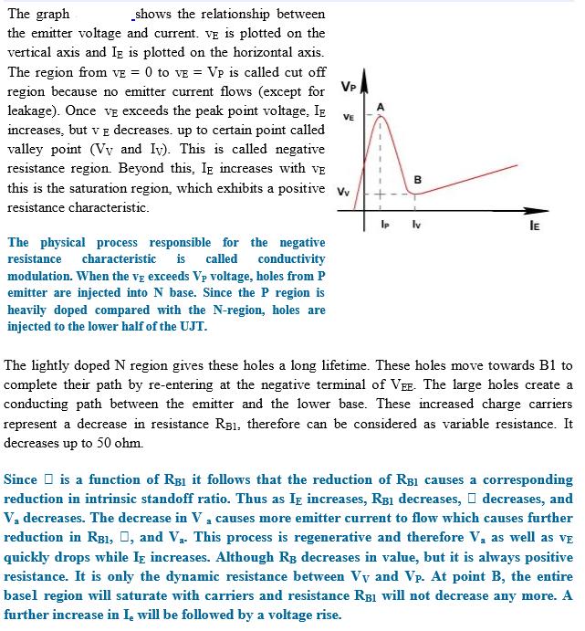
MAHALAKSHMI ENGINEERING COLLEGE TIRUCHIRAPALLI UNIT V BLOCKING OSCILLATORS AND TIME BASE GENERATORS
|
|
|
- Antony Cross
- 5 years ago
- Views:
Transcription


1 MAHALAKSHMI ENGINEERING COLLEGE TIRUCHIRAPALLI UNIT V BLOCKING OSCILLATORS AND TIME BASE GENERATORS PART A (2 Marks) 1. What is blocking oscillator? The circuit which uses a regenerative feedback, producing a single pulse or pulse train is called a blocking oscillator. 2. Which are the two important elements of a blocking oscillator? 1. Active element like transistor. 2. A pulse transformer. 3. What is the function of pulse transformer in blocking oscillator? A pulse transformer is used to couple output of the transistor back to the input. The nature of such feedback through pulse transformer is controlled by relative winding polarities of a pulse transformer. 4. What is pulse transformer? [APR-2004] A pulse transformer is basically a transformer which couples a source of pulses of electrical energy to the load, keeping the shape and other properties of pulses unchanged. The voltage level of the pulse can be raised or lowered by designing the proper turn s ratio for the pulse transformer. 5. State the features of pulse transformer. 1. Generally iron cored and small in size. 2. The leakage inductance is minimum. 3. The interwinding capacitance is low. 4. The cores have high permeability. 5. They have high magnetizing inductance. 6. Draw the equivalent circuit of pulse transformer. Explain the various elements in it.? [APR- 2004] In this circuit, R 1 = Resistance of primary winding. R 2 = Resistance referred to primary. σ = Series inductance which is leakage inductance. L = Shunt inductance which is magnetizing inductance. C = Transformer and external loading capacitive effect. 8. What is Leading edge response? At start there is an overshoot and then the pulse settles down. The response till it settles down after the overshoot is called leading edge response. 9. What is trailing edge response? The response generally extends below the zero amplitude after the end of pulse width is called back swing. The portion of response from backswing till it settles down is trailing edge response. 10. What is flat top response? The portion of the response between the trailing edge and the leading edge is called flat top response. 1
2 11. Define rise time of a pulse. The rise time is an important parameter related to this part of the response. It is defined by the time required by the pulse to rise from 10 % of its amplitude to 90 % of its amplitude. 12. Define the displacement error e d of a sweep voltage. (NOV-2003) It is defined as the maximum difference between the actual sweep voltage and linear sweep voltage which passes through the beginning and end points of the actual sweep. It is another way of specifying the linearity of a sweep waveform. 13. Mention the application of the pulse transformer.(nov-2003). 1. To change the amplitude and impedance level of a pulse. 2. To invert the polarity of the pulse. 3. To provide dc isolation between source and a load. 4. To differentiate a pulse. 5. for coupling the stages of a pulse amplifier 6. Also used in digital signal transmission. 14. What is current time base generator? The circuit which produces current which linearly increases with time is called current time base generator. 15. What are the applications of the blocking oscillator? (APRIL-2004) 1. The blocking oscillator can be used as low impedance switch used to discharge a capacitor very quickly. 2. To produce large peak power pulses, both the types of oscillators cab be used. 3. The output of the blocking oscillator can be used to produce gating waveform with very low mark space ratio. 4. It may be used as frequency divider or counter in digital circuits. 16. List varies sweep circuits Exponential charging circuit Constant-current charging circuit. Miller circuit boot strap circuit Inductor circuit. 17. What do you mean by voltage time base generators? Circuits used to generate a linear variation of voltage with time are called voltage time-base generators. 18. What do you mean by linear time base generator? Circuits provide an output waveform which exhibits a linear variation of voltage with time is called linear time base generators. 19. What is Blocking Oscillator? A special type of wave generator which is used to produce a single narrow pulse or train of pulses using regenerative feedback characteristics are called Blocking oscillator. 20. What are Time Base generators? The circuits which provide an output waveform, a part of which is characterized by a linear variation of voltage or current with respect to time are called Time Base generators. 2
3 21. What is UJT? 1. UJT is a three terminal semiconductor switching device. 2. As it has only one PN junction and three leads, it is commonly called as Uni-junction transistor. 22. What are the two important elements of Blocking Oscillator? Transistor and pulse transformer. 23. What are the applications of blocking Oscillator? It is used in frequency dividers, counter circuits and for switching the other circuits. 24. Give the expression for co-efficient of coupling K=M/ LpLs M-> Mututal Inductance, Lp -> Primary Inductance, Ls -> Secondary Inductance 25. Give the formula for transformation ratio n= Ns/Np = transformation ratio Ns= Secondary Turns; Np= Primary turns 26. Define rise time. It is defined by the time required by the pulse to rise from 10% of its amplitude to 90% of its amplitude. 27. Define overshoot. It is the amount by which the output exceeds its amplitude during first attempt. 28. What is leading edge response? At start there is an overshoot and then pulse settles down. The response till it settles down after the overshoot is called leading edge response. 29. What is trailing edge response? The response generally extends below the zero amplitude after the end of pulse width is called back swing. The portion of response from back swing till it settles down is called trailing edge response. 30. Define flat top response. The portion of the response between the trailing edge and the leading edge is called flat top response. 31. Define droop or a tilt. The displacement of the pulse amplitude during its flat response is called droop or a tilt. 32. What are the applications of pulse transformer? Pulse transformer can be used to 1. Change the amplitude and impedance level of a pulse. 2. Invert the polarity of the pulse. 3. Produce a pulse in a circuit having negligible d.c. resistance. 4. Differentiate a pulse. 5. Act as a coupling element in a certain pulse generating circuits. 3
4 33. When does the core saturate? When L->o as B-> Bm, the core saturates. 34. What is the other name of astable Blocking Oscillator? Free running blocking Oscillator. 35. What are the two types of astable Blocking Oscillator? 1. Diode controlled Astable Blocking Oscillator. 2. Re controlled Astable Blocking Oscillator. 36. Define Sweep time in saw tooth generator. The period during which voltage increases linearly is called sweep time. 37. What is the other name of saw tooth generator? Ramp generator. 38. Define Displacement error in the saw tooth generator? It is defined as the maximum differences between the actual sweep voltage and linear sweep which passes through the beginning and end points of the actual sweep. 39. What is constant current charging? A capacitor is charged with a constant current source. 40. What is the miller circuit? Integrator is used to convert a step waveform into ramp waveform. 41. Mention the various methods of controlling the pulse. 1. Use of common base configuration. 2. Use of common collector configuration. 3. Use of core saturation method. 4. Use of shorted delay line. 42. What is mark space ratio? The ratio of time for which Q is On to time for which Q is OFF is called mark- space ratio. If this is unity, then the output is almost symmetrical square wave. 43. Define Duty cycle. The duty cycle is defined as the ratio of the ON time tp to the time period T. Mathematically it is given by, D= tp/t. 44. How high duty cycle is obtained? 1. Using temperature compensated zener diode. 2. Using Ge diode in series with tertiary winding across the supply voltage. 45. What do you mean by voltage time base generators? Circuits used to generate a linear variation of voltage with time are called Voltage time-base generators. 46. What do you mean by linear time base generators/ Circuits provide an output waveform which exhibits a linear variation of voltage with time are called linear time base generators. 47. Define restoration time or flyback time. The time required for the return for the sweep voltage to the initial value is called restoration time (or) return time (or) flyback time. 4
5 48. Define sweep time. The period during which voltage increases linearly is called sweep time. 49. List important sweep parameters. Sweep speed error, Displacement error and transmission error. 50. Name the different errors in generation of sweep waveforms. Sweep speed error, Displacement error and transmission error. 51. Define Sweep speed error. It is the ratio of difference in slope at beginning and end of sweep to the initial value of slope. 52. Define Displacement error. It is defined as the maximum difference between the actual sweep voltage and linear sweep which passes through the beginning and end points of the actual sweep. 53. Define transmission error. When a ramp voltage is transmitted through a high-pass RC network, its output falls away from the input. The transmission error is defined as the difference between the input and output divided by the input. 5
6 Part B (16 Marks) 1. Explain the construction, equivalent circuit and operation of UJT. Draw the characteristics of UJT. 2. Explain how UJT is used to generate saw tooth waveform.(auc DEC 11) The UJT as the name implies, is characterized by a single pn junction. It exhibits negative resistance characteristic that makes it useful in oscillator circuits. The symbol for UJT is shown in fig. 1. The UJT is having three terminals base1 (B1), base2 (B2) and emitter (E). The UJT is made up of an N-type silicon bar which acts as the base as shown in fig. 2. It is very lightly doped. A P-type impurity is introduced into the base, producing a single PN junction called emitter. The PN junction exhibits the properties of a conventional diode. A complementary UJT is formed by a P-type base and N-type emitter. Except for the polarity of voltage and current the characteristic is similar to those of a conventional UJT. A simplified equivalent circuit for the UJT is shown in fig. 3. VBB is a source of biasing voltage connected between B2 and B1. When the emitter is open, the total resistance from B2 to B1 is simply the resistance of the silicon bar, this is known as the inter base resistance RBB. Since the N-channel is lightly doped, therefore RBB is relatively high, typically 5 to 10K ohm. RB2 is the resistance between B2 and point a', while RB1 is the resistance from point a' to B1, therefore the interbase resistance RBB is RBB = RB1 + RB2 6
7 7
8 8
9 9
10 10
11 11
12 3. write a note on waveform generator and time base generator. WAVEFORM GENERATOR Nonsinusoidal oscillators generate complex waveforms such as those just discussed. Because the outputs of these oscillators are generally characterized by a sudden change, or relaxation, these oscillators are often called RELAXATION OSCILLATORS. The pulse repetition rate of these oscillators is usually governed by the charge and discharge timing of a capacitor in series with a resistor. However, some oscillators contain inductors that, along with circuit resistance, affect the output frequency. These RC and LC networks within oscillator circuits are used for frequency determination. Within this category of relaxation oscillators are MULTIVIBRATORS, BLOCKING OSCILLATORS, and SAWTOOTH- and Trapezoidal-Wave Generators. Many electronic circuits are not in an "on" condition all of the time. In computers, for example, waveforms must be turned on and off for specific lengths of time. The time intervals vary from tenths of microseconds to several thousand microseconds. Square and rectangular waveforms are normally used to turn such circuits on and off because the sharp leading and trailing edges make them ideal for timing purposes. TIME-BASE GENERATORS Radar sets, oscilloscopes, and computer circuits all use sawtooth (voltage or current) waveforms. A sawtooth waveshape must have a linear rise. The sawtooth waveform is often used to produce a uniform,progressive movement of an electron beam across the face of an electrostatic cathode ray tube. This movement of the electron beam is known as a sweep. The voltage which causes this movement is known as sweep voltage and the circuit which produces this voltage is the sweep generator,or time-base generator. Most common types of time-base generators develop the sawtooth waveform by using some type of switching action with either the charge or discharge of an RC or RL circuit. 12
13 Sawtooth Wave A sawtooth wave can be generated by using an RC network. Possibly the simplest sawtooth generator. Assume that at T0, S1 is placed in position P. At the instant the switch closes, the applied voltage (Ea) appears at R. C begins to charge to E a through R. If S1 remains closed long enough, C will fully charge to Ea. You should remember from NEETS, Module 2, Alternating Current and Transformers, that a capacitor takes 5 time constants (5TC)to fully charge. As the capacitor charges to the applied voltage, the rate of charge follows an exponential curve. If a linear voltage is desired, the full charge time of the capacitor cannot be used because the exponential curve becomes nonlinear during the first time constant. UNIJUNCTION SAWTOOTH GENERATOR. When the 20 volts is applied across B2 and B1, the n-type bar acts as a voltage- divider. A voltage of 12.8 volts appears at a point near the emitter. At the first instant, C1 has no voltage across it, so the output of the circuit, which is taken across the capacitor (C1), is equal to 0 volts. (The voltage across C1 is also the voltage that is applied to the emitter of the unijunction.) The uni junction is now reverse biased. After T0, C1 begins to charge toward 20 volts.at T1, the voltage across the capacitor (the voltage on the emitter) has reached approximately 12.8 volts. This is the peak point for the uni junction, and it now becomes forward biased. With the emitter forward biased, the impedance between the emitter and B1 is just a few ohms. This is similar to placing a short across the capacitor. The capacitor discharges very rapidly through the low resistance of B1 to E. As C1 discharges, the voltage from the emitter to B1 also decreases. Q1 will continue to be forward biased as long as the voltage across C1 is larger than the valley point of the unijunction. At T2 the 3-volt valley point of the unijunction has been reached. The emitter now becomes reverse biased and the impedance from the emitter to B1 returns to a high value. Immediately after T2, Q1 is reverse biased and the capacitor has a charge of approximately 3 volts. C1 now starts to charge toward 20 volts. The circuit operation from now on is just a continuous repetition of the actions between T2 and T4.The capacitor charges until the emitter becomes forward biased, the unijunction conducts and C1discharges, and Q1 becomes reverse biased and C1 again starts charging. 13
14 Now, let's determine the linearity, electrical length, and amplitude of the output waveform. First, the linearity: To charge the circuit to the full 20 volts will take 5 time constants. In the circuit shown in figure 3-44, view (B), C1 is allowed to charge from T2 to T3. To find the percentage of charge, use the equation: This works out to be about 57 percent and is far beyond the 10 percent required for a linear sweep voltage. 14
15 The relaxation oscillator shown in figure consists of UJT and a capacitor C which is charged through resistor RE when inter base voltage VBB is switched on. During the charging period, the voltage across the capacitor increases exponentially until it attains the peak point voltage VP. When the capacitor voltage attains voltage VP, the UJT switches on and the capacitor C rapidly discharges through B1. The resulting current through the external resistor R develops a voltage spike, as illustrated in figure and the capacitor voltage drops to the value VV. The device then cuts off and the capacitor commences charging again. The cycle is repeated continually generating a saw-tooth waveform across capacitor C. The resulting waveforms of capacitor voltage VC and the voltage across resistor R (VR) are shown in figure. The frequency of the input saw-tooth wave can be varied by varying the value of resistor RE as it controls the time constant (T = REC) of the capacitor charging circuit. The discharge time t2 is difficult to calculate because the UJT is in its negative resistance region and its resistance is continually changing. However, t2 is normally very much less than t1 and can be neglected for approximation. For satisfactory operation of the above oscillator the following two conditions for the turn-on and turn-off of the UJT must be met. RE < VBB VP / IP and RE > VBB VV / IV That is the range of resistor RE should be as given below VBB VP / IP > RE > VBB VV / IV The time period and, therefore, frequency of oscillation can be derived as below. During charging of capacitor, the voltage across the capacitor is given as Vc = VBB(l-e-t/ReC) where REC is the time constant of the capacitor charging circuit and t is the time from the commencement of the charging.the discharge of the capacitor commences at the end of charging period t1 when the voltage across the capacitor Vc becomes equal to VP, that is, (Ƞ VBB + VB) VP = Ƞ VBB + VB = VBB(l-e-t/ReC) Neglecting VB in comparison to Ƞ VBB we have Ƞ VBB = VBB(l-e-t1/ReC) or e-t1/rec = 1 Ƞ So charging time period, t1 = 2.3 RE C log10 1/1- Ƞ 15
16 Since discharging time duration t2 is negligibly small as compared to charging time duration t1 so taking time period of the wave, T = t1 Time period of the saw-tooth wave, T = 2.3 RE C log10 1/1- Ƞ and frequency of oscillation f = 1/T = 1/2.3REClog10 (1-Ƞ) By including a small resistor in each base circuit, three useful outputs (saw-tooth waves, positive triggers, and negative triggers), as shown in figure, can be obtained. When the UJT fires, the surge of current through Bt causes a voltage drop across R1 and produces the positive going spikes. Also at the UJT firing time, the fall of VEB causes IB to rise rapidly and generate the negative-going spikes across R2, as shown in figure. R1 and R2 should be much smaller than RBB to avoid altering the firing voltage of the UJT. A wide range of oscillation frequencies can be achieved by making RE adjustable and including a switch to select different values of capacitance, as illustrated. As already mentioned in previous blog post there is upper and lower limits to the signal source resistance RE for the satisfactory operation of the UJT. 4. Pulse transformer: A pulse transformer is a transformer that is optimised for transmitting rectangular electrical pulses (that is, pulses with fast rise and fall times and a relatively constant amplitude). Small versions called signal types are used in digital logic and telecommunications circuits, often for matching logic drivers to transmission lines. Medium-sized power versions are used in power-control circuits such as camera flash controllers. Larger power versions are used in the electrical power distribution industry to interface low-voltage control circuitry to the high-voltage gates of power semiconductors. Special high voltage pulse transformers are also used to generate high power pulses for radar, particle accelerators, or other high energy pulsed power applications. To minimise distortion of the pulse shape, a pulse transformer needs to have low values ofleakage inductance and distributed capacitance, and a high open-circuit inductance. In power-type pulse transformers, a low coupling capacitance (between the primary and secondary) is important to protect the circuitry on the primary side from high-powered transients created by the load. 16
17 For the same reason, high insulation resistance and high breakdown voltage are required. A good transient response is necessary to maintain the rectangular pulse shape at the secondary, because a pulse with slow edges would create switching losses in the power semiconductors. The product of the peak pulse voltage and the duration of the pulse (or more accurately, the voltage-time integral) is often used to characterise pulse transformers. Generally speaking, the larger this product, the larger and more expensive the transformer. Pulse transformers by definition have a duty cycle of less than 0.5, whatever energy stored in the coil during the pulse must be "dumped" out before the pulse is fired again. 5. Blocking oscillator: The BLOCKING OSCILLATOR is a special type of wave generator used to produce a narrow pulse, or trigger. Blocking oscillators have many uses, most of which are concerned with the timing of some other circuit. They can be used as frequency dividers or counter circuits and for switching other circuits on and off at specific times. In a blocking oscillator the pulse width (pw), pulse repetition time (prt), and pulse repetition rate (prr) are all controlled by the size of certain capacitors and resistors and by the operating characteristics of the transformer. The transformer primary determines the duration and shape of the output. Transformer Action Figure 3-31, view (A), shows a transformer with resistance in both the primary and secondary circuits. If S1 is closed, current will flow through R1 and L1. As the current increases in L1, it induces a voltage into L2 and causes current flow through R2. The voltage induced into L2 depends on the ratio of turns between L1 and L2 as well as the current flow through L1. 17
18 The secondary load impedance, R2, affects the primary impedance through reflection from secondary to primary. If the load on the secondary is increased (R2 decreased), the load on the primary is also increased and primary and secondary currents are increased. T1 can be shown as an inductor and R1-R2 as a combined or equivalent series resistance (RE) since T1 has an effective inductance and any change in R1 or R2 will change the current. The equivalent circuit is shown in figure 3-31, view (B). It acts as a series RL circuit and will be discussed in those terms. Simple Series RL Circuit: When S1 is closed in the series RL circuit (view (B) of figure 3-31) L acts as an open at the first instant as source voltage appears across it. As current begins to flow, EL decreases and ER and I increase, all at exponential rates. Figure 3-32, view (A), shows these exponential curves. In a time equal to 5 time constants the resistor voltage and current are maximum and EL is zero. This relationship is shown in the following formula: 18
19 Voltage across a coil. If S1 is closed, as shown in figure 3-31, view (B), the current will follow curve 1 as shown in figure 3-32, view (A). The time required for the current to reach maximum depends on the size of L and RE. If RE is small, then the RL circuit has a long time constant. If only a small portion of curve 1 (C to D of view (A)) is used, then the current increase will have maximum change in a given time period. Further, the smaller the time increment the more nearly linear is the current rise. A constant current increase through the coil is a key factor in a blocking oscillator. 6. Application of blocking oscillator: A basic principle of inductance is that if the increase of current through a coil is linear; that is, the rate of current increase is constant with respect to time, then the induced voltage will be constant. This is true in both the primary and secondary of a transformer. Figure 3-32, view (B), shows the voltage waveform across the coil when the current through it increases at a constant rate. By definition, a blocking oscillator is a special type of oscillator which uses inductive regenerative feedback. The output duration and frequency of such pulses are determined by the characteristics of a transformer and its relationship to the circuit. When power is applied to the circuit, R1 provides forward bias and transistor Q1 conducts. Current flow through Q1 and the primary of T1 induces a voltage in L2. The phasing dots on the transformer indicate a 180-degree phase shift. As the bottom side of L1 is going negative, the bottom side of L2 is going positive. The positive voltage of L2 is coupled to the base of the transistor through C1, and Q1conducts more. This provides more collector current and more current through L1. This action is regenerative feedback. Very rapidly, sufficient voltage is applied to saturate the base of Q1. Once the base becomes saturated, it loses control over collector current. The circuit now can be compared to a small resistor (Q1) in series with a relatively large inductor (L1), or a series RL circuit. 19
20 The operation of the circuit to this point has generated a very steep leading edge for the output pulse.figure 3-34 shows the idealized collector and base waveforms. Once the base of Q1 becomes saturated, the current increase in L1 is determined by the time constant of L1 and the total series resistance. From T0 to T1 in figure 3-34 the current increase (not shown) is approximately linear. linear. The voltage across L1 will be a constant value as long as the current increase through L1 is At time T1, L1 saturates. At this time, there is no further change in magnetic flux and no coupling from L1 to L2. C1, which has charged during time TO to T1, will now discharge through R1 and cut off Q1. This causes collector current to stop, and the voltage across L1 returns to 0. The length of time between T0 and T1 (and T2 to T3 in the next cycle) is the pulse width, which depends mainly on the characteristics of the transformer and the point at which the transformer saturates. A transformer is chosen that will saturate at about 10 percent of the total circuit current. This ensures that the current increase is nearly linear. The transformer controls the pulse width because it controls the slope of collector current increase between points T0 and T1. Since TC = L R, the greater the L, the longer the TC. The longer the time constant, the slower the rate of current increase. When the rate of current increase is slow, the voltage across L1 is constant for a longer time. This primarily determines the pulse width. From T1 to T2 (figure 3-34), transistor Q1 is held at cutoff by C1 discharging through R1 (figure3-33). The transistor is now said to be "blocked." As C1 gradually loses its charge, the voltage on the base of Q1 returns to a forward-bias condition. At T2, the voltage on the base has become sufficiently positive to forward bias Q1, and the cycle is repeated. The collector waveform may have an inductive overshoot (parasitic oscillations)at the end of the pulse. when q1 cuts off, current through l1 ceases, and the magnetic field collapses,inducing a positive voltage at the collector of Q1. These oscillations are not desirable, so some means must be employed to reduce them. The transformer primary may be designed to have a high dc resistance resulting in a low Q; this resistance will decrease the amplitude of the oscillations. However, more damping may be necessary than such a low-q transformer primary alone can achieve. 20
21 If so, a DAMPING resistor can be placed in parallel with L1, When an external resistance is placed across a tank, the formula for the Q of the tank circuit is Q = R/XL, where R is the equivalent total circuit resistance in parallel with L. the Q is directly proportional to the damping resistance (R). In figure 3-35,damping resistor R2 is used to adjust the Q which reduces the amplitude of overshoot parasiticoscillations. As R2 is varied from infinity toward zero, the decreasing resistance will load the transformer to the point that pulse amplitude, pulse width, and prf are affected. If reduced enough, the oscillator will cease to function. By varying R2, varying degrees of damping can be achieved. The blocking oscillator discussed is a free-running circuit. For a fixed prf, some means of stabilizing the frequency is needed. One method is to apply external synchronization triggers (figure 3-37), view (A) and view (B). Coupling capacitor C2 feeds input synchronization (sync) triggers to the base of Q1. If the trigger frequency is made slightly higher than the free-running frequency, the blocking oscillator will "lock in" at the higher frequency. For instance, assume the free-running frequency of this blocking oscillator is 2 kilohertz, with a prt of 500 microseconds. If sync pulses with a prt of 400 microseconds, or 2.5 kilohertz, are applied to the base, the blocking oscillator will "lock in" and run at 2.5 kilohertz. If the sync prf is too high, however, frequency division will occur. This means that if the sync prt is too short, some of the triggers occur when the base is far below cutoff. The blocking oscillator may then synchronize with every second or third sync pulse. If trigger pulses are applied every 200 microseconds (5 kilohertz), the trigger that appears at T1 is not of sufficient amplitude to overcome the cutoff bias and turn on Q1. At T2, capacitor C1 has nearly discharged and the trigger causes Q1 to conduct. Note that with a 200-microsecond input trigger, the output prt is 400 microseconds. The output frequency is one-half the input trigger frequency and the blocking oscillator becomes a frequency divider. 21
NOORUL ISLAM COLLEGE OF ENGG, KUMARACOIL. DEPARTMENT OF ELECTRONICS AND COMMUNICATION ENGG. SUBJECT CODE: EC 1251 SUBJECT NAME: ELECTRONIC CIRCUITS-II
 NOORUL ISLAM COLLEGE OF ENGG, KUMARACOIL. DEPARTMENT OF ELECTRONICS AND COMMUNICATION ENGG. SUBJECT CODE: EC 1251 SUBJECT NAME: ELECTRONIC CIRCUITS-II Prepared by, C.P.SREE BALA LEKSHMI (Lect/ECE) ELECTRONICS
Basic Electronics Learning by doing Prof. T.S. Natarajan Department of Physics Indian Institute of Technology, Madras
 Basic Electronics Learning by doing Prof. T.S. Natarajan Department of Physics Indian Institute of Technology, Madras Lecture 38 Unit junction Transistor (UJT) (Characteristics, UJT Relaxation oscillator,
e base generators Tim 1
 Time base generators 1 LINEAR TIME BASE GENERATORS Circuits thatprovide An Output Waveform Which Exhibits Linear Variation Of Voltage or current With Time. Linear variation of Voltage :Voltage time base
LECTURE NOTES ELECTRONIC CIRCUITS II SYLLABUS
 FATIMA MICHAEL COLLEGE OF ENGINEERING & TECHNOLOGY Madurai Sivagangai Main Road Madurai - 625 020. [An ISO 9001:2008 Certified Institution] LECTURE NOTES EC6401 ELECTRONIC CIRCUITS - II SEMESTER: IV /
Oscillators. Hartley, Colpitts, UJT relaxation. ECE/MEA Engg College S.R.K. 9/13/2007 Authored by: Ramesh.K
 Oscillators Hartley, Colpitts, UJT relaxation. S.R.K 9//007 Authored by: Ramesh.K This documents contains a brief note about the principle of sinusoidal oscillator and some general oscillator circuits
Question Bank EC6401 ELECTRONIC CIRCUITS - II
 FATIMA MICHAEL COLLEGE OF ENGINEERING & TECHNOLOGY Madurai Sivagangai Main Road Madurai - 625 020. [An ISO 9001:2008 Certified Institution] SEMESTER: IV / ECE Question Bank EC6401 ELECTRONIC CIRCUITS -
Exam Booklet. Pulse Circuits
 Exam Booklet Pulse Circuits Pulse Circuits STUDY ASSIGNMENT This booklet contains two examinations for the six lessons entitled Pulse Circuits. The material is intended to provide the last training sought
SCR- SILICON CONTROLLED RECTIFIER
 SCR- SILICON CONTROLLED RECTIFIER Definition: When a pn junction is added to a junction transistor, the resulting three pn junction device is called a silicon controlled rectifier. SCR can change alternating
 SET - 1 1. a) Write the application of attenuator b) State the clamping theorem c) Write the application of Monostable multi vibrator d) Draw the diagram for Diode two input AND gate e) Define the terms
Unijunction Transistor. T.Y.B.Sc - Eletronics POWER ELETRONICS
 Unijunction Transistor T.Y.B.Sc - Eletronics POWER ELETRONICS Unijunction Transistor Symbol and Construction The Unijunction Transistor is solid state three terminal device that can be used in gate pulse,
Emitter base bias. Collector base bias Active Forward Reverse Saturation forward Forward Cut off Reverse Reverse Inverse Reverse Forward
 SEMICONDUCTOR PHYSICS-2 [Transistor, constructional characteristics, biasing of transistors, transistor configuration, transistor as an amplifier, transistor as a switch, transistor as an oscillator] Transistor
OBJECTIVE TYPE QUESTIONS
 OBJECTIVE TYPE QUESTIONS Q.1 The breakdown mechanism in a lightly doped p-n junction under reverse biased condition is called (A) avalanche breakdown. (B) zener breakdown. (C) breakdown by tunnelling.
BHARATHIDASAN ENGINEERING COLLEGE
 BHARATHIDASAN ENGINEERING COLLEGE DEPARTMENT OF ELECTRONICS AND COMMUNICATION ENGINEERING EC6401 - ELECTRONIC CIRCUITS - II QUESTION BANK II- YEAR IV SEM ACDEMIC YEAR: 2016-2017 EVEN SEMESTER EC6401 ELECTRONIC
DIGITAL ELECTRONICS WAVE SHAPING AND PULSE CIRCUITS. September 2012
 AM 5-403 DIGITAL ELECTRONICS WAVE SHAPING AND PULSE CIRCUITS September 2012 DISTRIBUTION RESTRICTION: Approved for public release. Distribution is unlimited. DEPARTMENT OF THE ARMY MILITARY AUXILIARY RADIO
State the application of negative feedback and positive feedback (one in each case)
") (ISO/IEC - 700-005 Certified) Subject Code: 073 Model wer Page No: / N Important Instructions to examiners: ) The answers should be examined by key words and not as word-to-word as given in the model answer
(ISO/IEC - 700-005 Certified) Subject Code: 073 Model wer Page No: / N Important Instructions to examiners: ) The answers should be examined by key words and not as word-to-word as given in the model answer
Difference between BJTs and FETs. Junction Field Effect Transistors (JFET)
") Difference between BJTs and FETs Transistors can be categorized according to their structure, and two of the more commonly known transistor structures, are the BJT and FET. The comparison between BJTs
Difference between BJTs and FETs Transistors can be categorized according to their structure, and two of the more commonly known transistor structures, are the BJT and FET. The comparison between BJTs
R05. For the circuit shown in fig.1, a sinusoidal voltage of peak 75V is applied. Assume ideal diodes. Obtain the output waveforms.
 Code.No: 33051 R05 SET-1 JAWAHARLAL NEHRU TECHNOLOGICAL UNIVERSITY HYDERABAD II.B.TECH - I SEMESTER SUPPLEMENTARY EXAMINATIONS NOVEMBER, 2009 (Common to EEE, ECE, EIE, ETM) Time: 3hours Max.Marks:80 Answer
VETRI VINAYAHA COLLEGE OF ENGINEERING & TECHNOLOGY THOTTIAM, TIRUCHIRAPPALLI Department of Electronics and communication Engineering Question
 VETRI VINAYAHA COLLEGE OF ENGINEERING & TECHNOLOGY THOTTIAM, TIRUCHIRAPPALLI-621215 Department of Electronics and communication Engineering Question Bank EC6401: ELECTRONIC CIRCUITS II (Regulation 2013)
Learn about the use, operation and limitations of thyristors, particularly triacs, in power control
 Exotic Triacs: The Gate to Power Control Learn about the use, operation and limitations of thyristors, particularly triacs, in power control D. Mohan Kumar Modern power control systems use electronic devices
The steeper the phase shift as a function of frequency φ(ω) the more stable the frequency of oscillation
 the more stable the frequency of oscillation") It should be noted that the frequency of oscillation ω o is determined by the phase characteristics of the feedback loop. the loop oscillates at the frequency for which the phase is zero The steeper the
It should be noted that the frequency of oscillation ω o is determined by the phase characteristics of the feedback loop. the loop oscillates at the frequency for which the phase is zero The steeper the
UNIT 2. Q.1) Describe the functioning of standard signal generator. Ans. Electronic Measurements & Instrumentation
 Describe the functioning of standard signal generator. Ans. Electronic Measurements & Instrumentation") UNIT 2 Q.1) Describe the functioning of standard signal generator Ans. STANDARD SIGNAL GENERATOR A standard signal generator produces known and controllable voltages. It is used as power source for the
UNIT 2 Q.1) Describe the functioning of standard signal generator Ans. STANDARD SIGNAL GENERATOR A standard signal generator produces known and controllable voltages. It is used as power source for the
REV NO EXPERIMENT NO 1 AIM: To study the PN junction diode characteristics under Forward & Reverse bias conditions. APPARATUS REQUIRED:
 KARNAL INSTITUTE OF TECHNOLOGY & MANAGEMENT KUNJPURA, KARNAL LAB MANUAL OF ------- SUBJECT CODE DATE OF ISSUE: SEMESTER: BRANCH: REV NO EXPERIMENT NO 1 AIM: To study the PN junction diode characteristics
Scheme Q.1 Attempt any SIX of following: 12-Total Marks a) Draw symbol NPN and PNP transistor. 2 M Ans: Symbol Of NPN and PNP BJT (1M each)
 Draw symbol NPN and PNP transistor. 2 M Ans: Symbol Of NPN and PNP BJT (1M each)") Q. No. WINTER 16 EXAMINATION (Subject Code: 17319) Model Answer Important Instructions to examiners: 1) The answers should be examined by key words and not as word-to-word as given in the model answer
Q. No. WINTER 16 EXAMINATION (Subject Code: 17319) Model Answer Important Instructions to examiners: 1) The answers should be examined by key words and not as word-to-word as given in the model answer
Multivibrators. Department of Electrical & Electronics Engineering, Amrita School of Engineering
 Multivibrators Multivibrators Multivibrator is an electronic circuit that generates square, rectangular, pulse waveforms. Also called as nonlinear oscillators or function generators. Multivibrator is basically
VALLIAMMAI ENGINEERING COLLEGE
 VALLIAMMAI ENGINEERING COLLEGE SRM Nagar, Kattankulathur 603 203. DEPARTMENT OF ELECTRONICS & COMMUNICATION ENGINEERING SUBJECT QUESTION BANK : EC6401 ELECTRONICS CIRCUITS-II SEM / YEAR: IV / II year B.E.
AE53/AC53/AT53/AE103 ELECT. DEVICES & CIRCUITS DEC 2015
 Q.2 a. By using Norton s theorem, find the current in the load resistor R L for the circuit shown in Fig.1. (8) Fig.1 IETE 1 b. Explain Z parameters and also draw an equivalent circuit of the Z parameter
 11. What is fall time (tf) in transistor? The time required for the collector current to fall from 90% to 10% of its DEPARTMENT OF ECE EC 6401 Electronic Circuits II UNIT-IV WAVE SHAPING AND MULTIVIBRATOR
UNDERSTANDING HORIZONTAL OUTPUT STAGES OF COMPUTER MONITORS
 UNDERSTANDING HORIZONTAL OUTPUT STAGES OF COMPUTER MONITORS Today's computer, medical, security, design and industrial video display monitors operate at a host of different horizontal resolutions or scanning
UNIT II JFET, MOSFET, SCR & UJT
 UNIT II JFET, MOSFET, SCR & UJT JFET JFET as an Amplifier and its Output Characteristics JFET Applications MOSFET Working Principles, SCR Equivalent Circuit and V-I Characteristics. SCR as a Half wave
Lecture (10) Power Amplifiers (2)
 Power Amplifiers (2)") Lecture (10) Power Amplifiers (2) By: Dr. Ahmed ElShafee ١ Class B/AB Power the ideal maximum peak output current for both dual supply and single supply push pull amplifiers is approximately Ic(sat), and
Lecture (10) Power Amplifiers (2) By: Dr. Ahmed ElShafee ١ Class B/AB Power the ideal maximum peak output current for both dual supply and single supply push pull amplifiers is approximately Ic(sat), and
GATE: Electronics MCQs (Practice Test 1 of 13)
") GATE: Electronics MCQs (Practice Test 1 of 13) 1. Removing bypass capacitor across the emitter leg resistor in a CE amplifier causes a. increase in current gain b. decrease in current gain c. increase
GATE: Electronics MCQs (Practice Test 1 of 13) 1. Removing bypass capacitor across the emitter leg resistor in a CE amplifier causes a. increase in current gain b. decrease in current gain c. increase
DLVP A OPERATOR S MANUAL
 DLVP-50-300-3000A OPERATOR S MANUAL DYNALOAD DIVISION 36 NEWBURGH RD. HACKETTSTOWN, NJ 07840 PHONE (908) 850-5088 FAX (908) 908-0679 TABLE OF CONTENTS INTRODUCTION...3 SPECIFICATIONS...5 MODE SELECTOR
Shankersinh Vaghela Bapu Institute of Technology INDEX
 Shankersinh Vaghela Bapu Institute of Technology Diploma EE Semester III 3330905: ELECTRONIC COMPONENTS AND CIRCUITS INDEX Sr. No. Title Page Date Sign Grade 1 Obtain I-V characteristic of Diode. 2 To
HIGH LOW Astable multivibrators HIGH LOW 1:1
 1. Multivibrators A multivibrator circuit oscillates between a HIGH state and a LOW state producing a continuous output. Astable multivibrators generally have an even 50% duty cycle, that is that 50% of
HEATHKIT ELECTRONIC KEYER HD-10
 HEATHKIT ELECTRONIC KEYER HD-10 CIRCUIT DESCRIPTION SCHEMATIC DIAGRAM The letter-number designations on the Schematic Diagram are used to identify resistors, capacitors and diodes. Each designation is
Chapter.8: Oscillators
 Chapter.8: Oscillators Objectives: To understand The basic operation of an Oscillator the working of low frequency oscillators RC phase shift oscillator Wien bridge Oscillator the working of tuned oscillator
BREAKDOWN DEVICES. Learning Objectives
 C H A P T E R64 Learning Objectives What are Breakdown Devices? Unijunction Transistor UJT Relaxation Oscillator Programmable UJT(PUT) Silicon Controlled Rectifier Comparison between Transistors and Thyristors
Chapter 8. Field Effect Transistor
 Chapter 8. Field Effect Transistor Field Effect Transistor: The field effect transistor is a semiconductor device, which depends for its operation on the control of current by an electric field. There
R a) Explain the operation of RC high-pass circuit when exponential input is applied.
 Explain the operation of RC high-pass circuit when exponential input is applied.") SET - 1 1. a) Explain the operation of RC high-pass circuit when exponential input is applied. 2x V ( e 1) V b) Verify V2 = = tanhx for a symmetrical square wave applied to a RC low 2x 2 ( e + 2 pass circuit.
SET - 1 1. a) Explain the operation of RC high-pass circuit when exponential input is applied. 2x V ( e 1) V b) Verify V2 = = tanhx for a symmetrical square wave applied to a RC low 2x 2 ( e + 2 pass circuit.
3. Diode, Rectifiers, and Power Supplies
 3. Diode, Rectifiers, and Power Supplies Semiconductor diodes are active devices which are extremely important for various electrical and electronic circuits. Diodes are active non-linear circuit elements
Power Amplifiers. Class A Amplifier
 Power Amplifiers The Power amplifiers amplify the power level of the signal. This amplification is done in the last stage in audio applications. The applications related to radio frequencies employ radio
Oscillators. An oscillator may be described as a source of alternating voltage. It is different than amplifier.
 Oscillators An oscillator may be described as a source of alternating voltage. It is different than amplifier. An amplifier delivers an output signal whose waveform corresponds to the input signal but
MAHARASHTRA STATE BOARD OF TECHNICAL EDUCATION (Autonomous) (ISO/IEC Certified) Summer 2016 EXAMINATIONS.
 (ISO/IEC Certified) Summer 2016 EXAMINATIONS.") Summer 2016 EXAMINATIONS Subject Code: 17321 Model Answer Important Instructions to examiners: 1) The answers should be examined by key words and not as word-to-word as given in the answer scheme. 2) The
Summer 2016 EXAMINATIONS Subject Code: 17321 Model Answer Important Instructions to examiners: 1) The answers should be examined by key words and not as word-to-word as given in the answer scheme. 2) The
Basic Electronics Prof. T.S. Natarajan Department of Physics Indian Institute of Technology, Madras
 Basic Electronics Prof. T.S. Natarajan Department of Physics Indian Institute of Technology, Madras Lecture 39 Silicon Controlled Rectifier (SCR) (Construction, characteristics (Dc & Ac), Applications,
Feedback Amplifier & Oscillators
 256 UNIT 5 Feedback Amplifier & Oscillators 5.1 Learning Objectives Study definations of positive /negative feedback. Study the camparions of positive and negative feedback. Study the block diagram and
UNIT-V: WAVEFORM GENERATORS AND SPECIAL FUNCTION ICs. PARTA (2 Marks)
") UNIT-V: WAVEFORM GENERATORS AND SPECIAL FUNCTION ICs PARTA (2 Marks) 1. Define line regulation.[auc April 2004] It is defined as the percentage change in the output voltage from a change in the input voltage.
UNIT-V: WAVEFORM GENERATORS AND SPECIAL FUNCTION ICs PARTA (2 Marks) 1. Define line regulation.[auc April 2004] It is defined as the percentage change in the output voltage from a change in the input voltage.
THIRD SEMESTER DIPLOMA EXAMINATION IN ELECTRICAL & ELECTRONICS ENGINEERING, MARCH 2013 ELECTRONIC DEVICES AND CIRCUITS
 REVISION-2010 Reg. No SUB CODE:3053 Signature THIRD SEMESTER DIPLOMA EXAMINATION IN ELECTRICAL & ELECTRONICS ENGINEERING, MARCH 2013 ELECTRONIC DEVICES AND CIRCUITS Time :3hours Maximum marks:100 PART
MARIA COLLEGE OF ENGINEERING AND TECHNOLOGY, ATTOOR UNIT-1. Feedback Amplifiers
 MARIA COLLEGE OF ENGINEERING AND TECHNOLOGY, ATTOOR DEPARTMENT OF ELECTRONICS AND COMMUNICATION ENGINEERING ELECTRONIC CIRCUITS-II 2 MARKS QUESTIONS & ANSWERS UNIT-1 Feedback Amplifiers 1. What is meant
DOWNLOAD PDF POWER ELECTRONICS DEVICES DRIVERS AND APPLICATIONS
 Chapter 1 : Power Electronics Devices, Drivers, Applications, and Passive theinnatdunvilla.com - Google D Download Power Electronics: Devices, Drivers and Applications By B.W. Williams - Provides a wide
Analog Circuits Prof. Jayanta Mukherjee Department of Electrical Engineering Indian Institute of Technology - Bombay
 Analog Circuits Prof. Jayanta Mukherjee Department of Electrical Engineering Indian Institute of Technology - Bombay Week - 08 Module - 04 BJT DC Circuits Hello, welcome to another module of this course
Gechstudentszone.wordpress.com
 Unit 1: Transistor, UJT s, and Thyristors In the Diode tutorials we saw that simple diodes are made up from two pieces of semiconductor material, either silicon or germanium to form a simple PN-junction
Project (02) Dc 2 AC Inverter
 Dc 2 AC Inverter") Project (02) Dc 2 AC Inverter By: Dr. Ahmed ElShafee 1 12v DC to 220v AC Converter Circuit Using Astable Multivibrator Inverter circuits can either use thyristors as switching devices or transistors. Normally
Project (02) Dc 2 AC Inverter By: Dr. Ahmed ElShafee 1 12v DC to 220v AC Converter Circuit Using Astable Multivibrator Inverter circuits can either use thyristors as switching devices or transistors. Normally
Bipolar Junction Transistors
 Bipolar Junction Transistors Invented in 1948 at Bell Telephone laboratories Bipolar junction transistor (BJT) - one of the major three terminal devices Three terminal devices more useful than two terminal
Gechstudentszone.wordpress.com
 8.1 Operational Amplifier (Op-Amp) UNIT 8: Operational Amplifier An operational amplifier ("op-amp") is a DC-coupled high-gain electronic voltage amplifier with a differential input and, usually, a single-ended
Power Semiconductor Devices
 TRADEMARK OF INNOVATION Power Semiconductor Devices Introduction This technical article is dedicated to the review of the following power electronics devices which act as solid-state switches in the circuits.
CMOS Schmitt Trigger A Uniquely Versatile Design Component
 CMOS Schmitt Trigger A Uniquely Versatile Design Component INTRODUCTION The Schmitt trigger has found many applications in numerous circuits, both analog and digital. The versatility of a TTL Schmitt is
PAiA 4780 Twelve Stage Analog Sequencer Design Analysis Originally published 1974
 PAiA 4780 Twelve Stage Analog Sequencer Design Analysis Originally published 1974 DESIGN ANALYSIS: CLOCK As is shown in the block diagram of the sequencer (fig. 1) and the schematic (fig. 2), the clock
Government Polytechnic Muzaffarpur Name of the Lab: Applied Electronics Lab
 Government Polytechnic Muzaffarpur Name of the Lab: Applied Electronics Lab Subject Code: 1620408 Experiment-1 Aim: To obtain the characteristics of field effect transistor (FET). Theory: The Field Effect
A simple and compact high-voltage switch mode power supply for streak cameras
 Meas. Sci. Technol. 7 (1996) 1668 1672. Printed in the UK DESIGN NOTE A simple and compact high-voltage switch mode power supply for streak cameras M Shukla, V N Rai and H C Pant Laser Plasma Group, Center
Subject Code: Model Answer Page No: / N
 Important Instructions to examiners: 1) The answers should be examined by key words and not as word-to-word as given in the model answer scheme. 2) The model answer and the answer written by candidate
Testing and Stabilizing Feedback Loops in Today s Power Supplies
 Keywords Venable, frequency response analyzer, impedance, injection transformer, oscillator, feedback loop, Bode Plot, power supply design, open loop transfer function, voltage loop gain, error amplifier,
SET - 1 Code No: II B. Tech II Semester Regular Examinations, April/May 2009
 SET - 1 Code No: 3220401 II B. Tech II Semester Regular Examinations, April/May 2009 PULSE AND DIGITAL CIRCUITS ( Common to E.C.E, B.M.E, E.Con.E, I.C.E ) Time: 3 hours Max Marks: 80 Answer Any FIVE Questions
PCB layout guidelines. From the IGBT team at IR September 2012
 PCB layout guidelines From the IGBT team at IR September 2012 1 PCB layout and parasitics Parasitics (unwanted L, R, C) have much influence on switching waveforms and losses. The IGBT itself has its own
Operational Amplifiers
 Operational Amplifiers Table of contents 1. Design 1.1. The Differential Amplifier 1.2. Level Shifter 1.3. Power Amplifier 2. Characteristics 3. The Opamp without NFB 4. Linear Amplifiers 4.1. The Non-Inverting
INTEGRATED CIRCUITS. AN1221 Switched-mode drives for DC motors. Author: Lester J. Hadley, Jr.
 INTEGRATED CIRCUITS Author: Lester J. Hadley, Jr. 1988 Dec Author: Lester J. Hadley, Jr. ABSTRACT The purpose of this paper is to demonstrate the use of integrated switched-mode controllers, generally
CHAPTER 2 A SERIES PARALLEL RESONANT CONVERTER WITH OPEN LOOP CONTROL
 14 CHAPTER 2 A SERIES PARALLEL RESONANT CONVERTER WITH OPEN LOOP CONTROL 2.1 INTRODUCTION Power electronics devices have many advantages over the traditional power devices in many aspects such as converting
TUNED AMPLIFIERS 5.1 Introduction: Coil Losses:
 TUNED AMPLIFIERS 5.1 Introduction: To amplify the selective range of frequencies, the resistive load R C is replaced by a tuned circuit. The tuned circuit is capable of amplifying a signal over a narrow
UNIT 1. 9 What is the Causes of Free Response in Electrical Circuit. 12 Write the Expression for transient current and voltages of RL circuit.
 SUB: Electric Circuits and Electron Devices Course Code: UBEE309 UNIT 1 PART A 1 State Transient and Transient Time? 2 What is Tansient State? 3 What is Steady State? 4 Define Source Free Response 5 Define
WINTER 17 EXAMINATION Subject Name: Basic Electronics Model Answer Sub Code:
 Important Instructions to examiners: 1) The answers should be examined by key words and not as word-to-word as given in the model answer scheme. 2) The model answer and the answer written by candidate
the reactance of the capacitor, 1/2πfC, is equal to the resistance at a frequency of 4 to 5 khz.
 EXPERIMENT 12 INTRODUCTION TO PSPICE AND AC VOLTAGE DIVIDERS OBJECTIVE To gain familiarity with PSPICE, and to review in greater detail the ac voltage dividers studied in Experiment 14. PROCEDURE 1) Connect
Experiment (1) Principles of Switching
 Principles of Switching") Experiment (1) Principles of Switching Introduction When you use microcontrollers, sometimes you need to control devices that requires more electrical current than a microcontroller can supply; for this,
Experiment (1) Principles of Switching Introduction When you use microcontrollers, sometimes you need to control devices that requires more electrical current than a microcontroller can supply; for this,
In addition to the power circuit a commercial power supply will require:
 Power Supply Auxiliary Circuits In addition to the power circuit a commercial power supply will require: -Voltage feedback circuits to feed a signal back to the error amplifier which is proportional to
Semiconductor theory predicts that the current through a diode is given by
 3 DIODES 3 Diodes A diode is perhaps the simplest non-linear circuit element. To first order, it acts as a one-way valve. It is important, however, for a wide variety of applications, and will also form
INSTITUTE OF AERONAUTICAL ENGINEERING (AUTONOMOUS) Dundigal, Hyderabad
 Dundigal, Hyderabad") INSTITUTE OF AERONAUTICAL ENGINEERING (AUTONOMOUS) Dundigal, Hyderabad - 500 043 CIVIL ENGINEERING ASSIGNMENT Name : Electrical and Electronics Engineering Code : A30203 Class : II B. Tech I Semester Branch
INSTITUTE OF AERONAUTICAL ENGINEERING (AUTONOMOUS) Dundigal, Hyderabad - 500 043 CIVIL ENGINEERING ASSIGNMENT Name : Electrical and Electronics Engineering Code : A30203 Class : II B. Tech I Semester Branch
Electro - Principles I
 The PN Junction Diode Introduction to the PN Junction Diode Note: In this chapter we consider conventional current flow. Page 11-1 The schematic symbol for the pn junction diode the shown in Figure 1.
ASTABLE MULTIVIBRATOR
 555 TIMER ASTABLE MULTIIBRATOR MONOSTABLE MULTIIBRATOR 555 TIMER PHYSICS (LAB MANUAL) PHYSICS (LAB MANUAL) 555 TIMER Introduction The 555 timer is an integrated circuit (chip) implementing a variety of
Paper-1 (Circuit Analysis) UNIT-I
 UNIT-I") Paper-1 (Circuit Analysis) UNIT-I AC Fundamentals & Kirchhoff s Current and Voltage Laws 1. Explain how a sinusoidal signal can be generated and give the significance of each term in the equation? 2. Define
Paper-1 (Circuit Analysis) UNIT-I AC Fundamentals & Kirchhoff s Current and Voltage Laws 1. Explain how a sinusoidal signal can be generated and give the significance of each term in the equation? 2. Define
GATE SOLVED PAPER - IN
 YEAR 202 ONE MARK Q. The i-v characteristics of the diode in the circuit given below are : v -. A v 0.7 V i 500 07 $ = * 0 A, v < 0.7 V The current in the circuit is (A) 0 ma (C) 6.67 ma (B) 9.3 ma (D)
Unit/Standard Number. LEA Task # Alignment
 1 Secondary Competency Task List 100 SAFETY 101 Demonstrate an understanding of State and School safety regulations. 102 Practice safety techniques for electronics work. 103 Demonstrate an understanding
Lecture (09) Bipolar Junction Transistor 3
 Bipolar Junction Transistor 3") Lecture (09) Bipolar Junction Transistor 3 By: Dr. Ahmed ElShafee ١ I THE BJT AS AN AMPLIFIER Amplification is the process of linearly increasing the amplitude of an electrical signal and is one of the
Lecture (09) Bipolar Junction Transistor 3 By: Dr. Ahmed ElShafee ١ I THE BJT AS AN AMPLIFIER Amplification is the process of linearly increasing the amplitude of an electrical signal and is one of the
Teccor brand Thyristors AN1001
 A1001 Introduction The Thyristor family of semiconductors consists of several very useful devices. The most widely used of this family are silicon controlled rectifiers (SCRs), Triacs, SIDACs, and DIACs.
Communication Circuit Lab Manual
 German Jordanian University School of Electrical Engineering and IT Department of Electrical and Communication Engineering Communication Circuit Lab Manual Experiment 2 Tuned Amplifier Eng. Anas Alashqar
DESIGN TIP DT Variable Frequency Drive using IR215x Self-Oscillating IC s. By John Parry
 DESIGN TIP DT 98- International Rectifier 233 Kansas Street El Segundo CA 9245 USA riable Frequency Drive using IR25x Self-Oscillating IC s Purpose of this Design Tip By John Parry Applications such as
Practical Testing Techniques For Modern Control Loops
 VENABLE TECHNICAL PAPER # 16 Practical Testing Techniques For Modern Control Loops Abstract: New power supply designs are becoming harder to measure for gain margin and phase margin. This measurement is
MAHARASHTRA STATE BOARD OF TECHNICAL EDUCATION (Autonomous) (ISO/IEC Certified)
 (ISO/IEC Certified)") WINTER 16 EXAMINATION Model Answer Subject Code: 17213 Important Instructions to examiners: 1) The answers should be examined by key words and not as word-to-word as given in the model answer scheme. 2)
WINTER 16 EXAMINATION Model Answer Subject Code: 17213 Important Instructions to examiners: 1) The answers should be examined by key words and not as word-to-word as given in the model answer scheme. 2)
Dr.Arkan A.Hussein Power Electronics Fourth Class. Commutation of Thyristor-Based Circuits Part-I
 Commutation of Thyristor-Based Circuits Part-I ١ This lesson provides the reader the following: (i) (ii) (iii) (iv) Requirements to be satisfied for the successful turn-off of a SCR The turn-off groups
RECTIFIERS AND POWER SUPPLIES
 UNIT V RECTIFIERS AND POWER SUPPLIES Half-wave, full-wave and bridge rectifiers with resistive load. Analysis for Vdc and ripple voltage with C,CL, L-C and C-L-C filters. Voltage multipliers Zenerdiode
Designing and Implementing of 72V/150V Closed loop Boost Converter for Electoral Vehicle
 International Journal of Current Engineering and Technology E-ISSN 77 4106, P-ISSN 347 5161 017 INPRESSCO, All Rights Reserved Available at http://inpressco.com/category/ijcet Research Article Designing
MAHALAKSHMI ENGINEERING COLLEGE TIRUCHIRAPALLI UNIT III TUNED AMPLIFIERS PART A (2 Marks)
") MAHALAKSHMI ENGINEERING COLLEGE TIRUCHIRAPALLI-621213. UNIT III TUNED AMPLIFIERS PART A (2 Marks) 1. What is meant by tuned amplifiers? Tuned amplifiers are amplifiers that are designed to reject a certain
MAHALAKSHMI ENGINEERING COLLEGE TIRUCHIRAPALLI-621213. UNIT III TUNED AMPLIFIERS PART A (2 Marks) 1. What is meant by tuned amplifiers? Tuned amplifiers are amplifiers that are designed to reject a certain
PAST EXAM PAPER & MEMO N3 ABOUT THE QUESTION PAPERS:
 EKURHULENI TECH COLLEGE. No. 3 Mogale Square, Krugersdorp. Website: www. ekurhulenitech.co.za Email: info@ekurhulenitech.co.za TEL: 011 040 7343 CELL: 073 770 3028/060 715 4529 PAST EXAM PAPER & MEMO N3
UNIVERSITY OF BRITISH COLUMBIA
 UNIVERSITY OF BRITISH COLUMBIA DEPARTMENT OF ELECTRICAL AND COMPUTER ENGINEERING POWER ELECTRONICS LAB HANDBOOK Dr P.R. Palmer Dr P.R. Palmer 1 2004 1 AIM The aim of the project is to design, construct
After the initial bend, the curves approximate a straight line. The slope or gradient of each line represents the output impedance, for a particular
 BJT Biasing A bipolar junction transistor, (BJT) is very versatile. It can be used in many ways, as an amplifier, a switch or an oscillator and many other uses too. Before an input signal is applied its
DEFINITION: Classification of oscillators Based on the frequency generated Oscillator type Frequency range
 DEFINITION: An oscillator is just an electronic circuit which converts dc energy into AC energy of required frequency. (Or) An oscillator is an electronic circuit which produces an ac output without any
Electronic PRINCIPLES
 MALVINO & BATES Electronic PRINCIPLES SEVENTH EDITION Chapter 22 Nonlinear Op-Amp Circuits Topics Covered in Chapter 22 Comparators with zero reference Comparators with non-zero references Comparators
Devices and Op-Amps p. 1 Introduction to Diodes p. 3 Introduction to Diodes p. 4 Inside the Diode p. 6 Three Diode Models p. 10 Computer Circuit
 Contents p. v Preface p. ix Devices and Op-Amps p. 1 Introduction to Diodes p. 3 Introduction to Diodes p. 4 Inside the Diode p. 6 Three Diode Models p. 10 Computer Circuit Analysis p. 16 MultiSIM Lab
TUNED AMPLIFIERS. Tank circuits.
 Tank circuits. TUNED AMPLIFIERS Analysis of single tuned amplifier, Double tuned, stagger tuned amplifiers. Instability of tuned amplifiers, stabilization techniques, Narrow band neutralization using coil,
Electronic Circuits ELECTRONIC CIRCUITS. Subject Code: 10CS32 I.A. Marks : 25 Hours/Week : 04 Exam Hours: 03 Total Hours : 52 Exam Marks: 100
 ELECTRONIC CIRCUITS Subject Code: I.A. Marks : 5 Hours/Week : 04 Exam Hours: 03 Total Hours : 5 Exam Marks: 00 UNIT PART - A 7 Hours Transistors, UJTs, and Thyristors: Operating Point, Common-EmitterConfiguration,
Laboratory Exercise 6 THE OSCILLOSCOPE
 Introduction Laboratory Exercise 6 THE OSCILLOSCOPE The aim of this exercise is to introduce you to the oscilloscope (often just called a scope), the most versatile and ubiquitous laboratory measuring
Q1 A) Attempt any six: i) Draw the neat symbol of N-channel and P-channel FET
 Attempt any six: i) Draw the neat symbol of N-channel and P-channel FET") Subject Code:17319 Model Answer Page1 of 27 Important Instructions to examiners: 1) The answers should be examined by key words and not as word-to-word as given in the model answer scheme. 2) The model
Subject Code:17319 Model Answer Page1 of 27 Important Instructions to examiners: 1) The answers should be examined by key words and not as word-to-word as given in the model answer scheme. 2) The model
Testing and Verification Waveforms of a Small DRSSTC. Part 1. Steven Ward. 6/24/2009
 Testing and Verification Waveforms of a Small DRSSTC Part 1 Steven Ward www.stevehv.4hv.org 6/24/2009 Power electronics, unlike other areas of electronics, can be extremely critical of small details, since