INF4420 Layout and CMOS processing technology
|
|
|
- Lenard Black
- 5 years ago
- Views:
Transcription
1 INF4420 Layout and CMOS processing technology Spring 2012 Jørgen Andreas Michaelsen
2 Outline CMOS Fabrication overview Design rules Layout of passive and active componets Packaging
3 Introduction As circuit designers we must carefully consider how to draw layout for critical/sensitive parts of the circuit in order to get robust and predictable performance. To be sucessfull at this, we must have a basic understanding of how circuits are manufactured, packaged, tested, and even how the circuit eventually is used on a PCB (e.g. external parasitics that we need to drive off
 layer")

4 Physical design The physical circuit is built on a disc of silicon (wafer) layer by layer. Some layers are implanted in the substrate, other layers are stacked on top.
5 Physical design How do we go from a layout (GDS2) to a physical circuit? For each step in the processing, we must get the relevant part of the design onto the wafer, do the processing (implant, etch, or grow), and ready the wafer for the next step.

 is")
6 Physical design Layout is "encoding" the physical realization of circuits. CMOS processing (manufacturing) is done in layers, so is layout.
7 Photolithography Photolithography (litho) is used to define regions for each layer. For each processing step, we need to transfer the mask onto the wafer (selectively coat/shield part of the wafer). Light source and a mask defines patterns on photoresist. Photoresist hardens when exposed to light.
 used for photolithography is")
8 Lithography system We create layout. The mask (or reticle) used for photolithography is derived from the layout.
, leaving a developed mask on the wafer.")
 After processing step, hardened resist is also removed.")
9 Photoresist (1) Photoresist hardens when exposed to light (negative photoresist), leaving a developed mask on the wafer. Remaining photoresist is removed. (2) Do processing. (3) After processing step, hardened resist is also removed. Repeat for all processing steps required for full circuit.
.")

10 Diffraction Slits in the reticle cause diffraction (pattern spreads out). Wavelength of light is a limitation for feature size. Images illustrating diffraction from Wikipedia. org.
 of the lens (angle of light captured by the lens, and refractive")
11 Resolution Resolution is limited by the wavelength of light and numerical aperture (NA) of the lens (angle of light captured by the lens, and refractive index n).
12 Depth of focus As the wafer is built layer by layer, geometry becomes uneven. Wavelength of light and NA will limit the allowed topology difference. Planarize wafer between processing steps (before imaging) with chemical mechanical polishing (CMP). Unfortunately, inherent tradeoff between DOF and resolution (better NA, finer pitch, more narrow DOF).
, sub resolution assist features (SRAF).")

13 Reducing k1 Optical proximity correction (OPC), sub resolution assist features (SRAF). Modelling the lithography as a non-linear low-pass 2D spatial filter, try to come up with an inverse.
14 Reducing k1 Phase shifting masks (PSM) Instead of "binary" on/off masks, masks alter the phase of the light. Double patterning Split layout accross two (or more) masks Off-axis illumination Optimizing the shape of the light source
15 Reducing k1 Result: k1=0.25 instead of k1=0.5 Restricting allowed pitch may be neccessary for pattern fidelity. Additionally, NA is improved through immersion lithography (water between lens and wafer, higher refractive index, n).
16 Extreme UV source 20 nm process with 193 nm light source? It can be done without defying the laws of physics! Why not use 13.5 nm (EUV) instead?


17 Front end of line (FEOL) Process modules that form the active devices Active area Channel doping Gate Source/drain extension Spacer Junction Silicide

18 Active area definition Shallow trench isoloation (STI) Insulation between active devices Etch trenches in the substrate Filled with SiO2
19 Channel doping Define p- and n-type regions for NMOS and PMOS
20 Gate electrode Gates made of polysilicon
21 Source/drain extension Mitigate short-channel effects source/drain resistance leakage current, drive current

22 Spacers Avoid bridging S/D and gate due to silicide Offset junctions (next step)
23 Junctions Source and drain junctions Implant arsenic/phosphore (n-type) or boron (p-type)
24 Silicide Lower resistance, better Ion. Avoid current crowding. Self aligned silicide = salicide
25 Back end of line (BEOL) Back end of line adds connection between devices, contacts and metal layers with vias between layers Parasitic resistance and capacitance is challenging for scaled technology. In modern CMOS, copper (Cu) metallization and low k dielectric is used.
26 BEOL modules Pre Metal Dielectric (PMD) Contacts to source, drain, and gate (tungsten) Inter Level Dielectric (ILD) Vias and metal lines (copper)

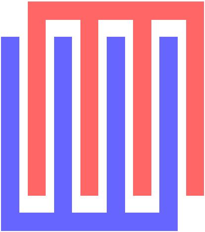
27 Dual Damascene Metallization used to be etching away aluminum. Impossible with copper. Instead: Damascene. Used throughout the BEOL. Image: wikipedia.org (1) Etch trenches in oxide, (2) deposit copper, (3) polish away the overfill (CMP)
 is deposited through electroplating (leaving excess Cu) 3.")
28 Dual Damascene 1. Trenches are etched in the oxide (to the barrier) 2. Metal (Cu) is deposited through electroplating (leaving excess Cu) 3. CMP to remove excess metal. Dual = via and metal
29 Dual Damascene Why should we as designers care? CMP polish rate is pattern dependent, i.e width and spacing of metal lines matter. Poor layout results in metal lines that are too thin and/or less dielectric separation of metal layers. Layout dependent delay. Post-layout simulation does not neccessarily reveal these problems.


30 Dishing and erosion Dishing affecting wide metal lines (Cu polishes faster than dielectric) Erosion affecting high density metal pattern
31 Drawing layout Layout is drawing the masks used in the manufacturing process. As we have seen, the layout we draw is not perfectly reproduced on the wafer. We must comply with a set of rules to ensure that the layout we draw is manufacturable.

32 Design rule examples Rule name (minimum) P.1 Poly width P.2 Space poly and active P.3 Poly ext. beyond active P.4 Enc. active around gate P.5 Spc. field poly to active P.6 Spc. field poly
33 Design rule examples Poly rules example (FreePDK45) Rule name (minimum) Length P.1 Poly width 50 nm P.2 Space poly and active 140 nm P.3 Poly extension beyond active 55 nm P.4 Enclosure active around gate 70 nm P.5 Space field poly to active 50 nm P.6 Space field poly 75 nm
34 Design rule examples Metal1 rules example (FreePDK45) Rule name (minimum) Length M1.1 Metal1 width 65 nm M1.2 Space metal1 65 nm M1.3 Enclosure around contact (two opposite sides) 35 nm M1.4 Enclosure around via1 on two opposite sides 35 nm M1.5 Space metal1 wider than 90 nm and longer than 900 nm 90 nm M1.6 Space metal1 wider than 270 nm and longer than 300 nm 270 nm M1.7 Space metal1 wider than 500 nm and longer than 1.8 um 500nm
35 Density design rules In addition to spacing and area rules. There are density rules. Ref. dishing and erosion resulting from CMP. Typically, the layout will undergo dummy fill to comply with density rules (automatic). Neccessary for manufacturability, but increases capacitance.
36 Antenna design rules Large area metal connected to a MOSFET gate can collect ions during manufacturing and irreversibly break down gate oxide.
37 Design rule switches Different set of rules can be invoked for different parts of the circuit. E.g. Minimum rules for high density generic digital circuitry Analog or DFM rules for sensitive circuits.
38 Used to be pass/fail, more recently reporting level of severity. Some rules can be waived. Design Rule Check, DRC Design Rule Check (DRC) Large number of rules to comply with. Difficult to keep track of. Automated by design tools with foundry rule set.
39 Litho friendly design, LFD Design rules does not guarantee a robust design or good yield. Possible to simulate and analyze how the layout will print on the wafer. Difficult to get access to data. Non-linear 2D spatial filter.

40 Lithography simulation Litho simulation using FreePDK45 and Calibre (

41 Lithography simulation Litho simulation using FreePDK45 and Calibre (
42 Layout vs. schematics, LVS Recognizing shapes in the layout (transistors and passive devices), and how they are connected. Comparing layout netlist to schematics.
43 Post layout simulation Extracts layout dependent parasitics (capacitance and resistance), and some layout dependent transistor parameters (e.g. LOD which we will discuss in the short-channel lecture). More accurate simulation results (but does not include all effects). Also, parasitics have fast/slow corners, temperature dependence. Results in slow simulation due to large netlists.
44 Interconnect Drawing metal "wires" in the layout is not like wires in the schematic. Must think about resistance, capacitance, and inductance. (E.g. 0.1 Ω/ for metal, and 10 Ω for via) Crosstalk and ground bounce. Decoupling.
45 Interconnect Single via approximately 10 Ω. Worse, single via failure. Not only resistance, but limitaions on current capability (electromigration). Process documentation should list actual values for a given process.


46 Interconnect Overlap capacitance low-k dielectric helps reduce interconnect capacitance Additionally, fringe capacitance also important.
47 Interconnect Sizing metal lines is a tradeoff between capcitance vs resistance (and current handling capability). Wide lines, fewer squares, less resistance, but potentially more overlap capacitance. Finally, to make it even more complicated, resistance and capacitance will vary due to dishing and erosion.
48 Passive components Mixed signal and analog require passive components (resistors, capacitors). RF needs inductors. Why not use parasitic resistance and capacitance? Possible in some cases.
49 Resistors Several possibilities. Need to consider: Ω/ (area, practical limit for large R) Temperature dependence (TC) Voltage dependence (linearity) Mismatch (ΔR/R, abs value +/- 20 %) Parasitic capacitance The TC and voltage dependence is not only linear, but also quadratic in the simulator. E.g. R(T) = R(T0) [1 + TC1(T-T0) + TC2(T-T0)^2]. Similar for voltage dependency.
50 Resistors Realistic alternatives for large resistors: N-well: Large R, poor TC (> 2000 ppm/c), poor linearity (< 1 %), low mismatch, parasitic capacitance from pn-depletion. Always available. Poly with silicide block: Large R, good TC (~ 100 ppm/c), reasonable linearity (< 0.1 %), low mismatch. Extra layer needed.
51 Capacitors Need to consider: F/m^2 Temperature dependence (TC) Voltage dependence (linearity) Mismatch (ΔR/R) Cost
52 Capacitors MOSCAP, using a mosfet as a capacitor (Cox). High capacitance per area, very non-linear, good e.g. for decoupling, but gate leakage current is problematic. PiP, using two poly layers. Usually not available in modern CMOS processes.
53 Capacitors MiM (Metal-insulator-Metal). Requires extra mask. ~ 1 or few ff/um^2. Good option if available. Thin separation of metal layers and special dielectric. Usually available in RF process flavours. Cost issue. MoM (Metal-oxide-Metal). Exploit fine pitch in CMOS. No extra processing required.

54 MoM Capactiors
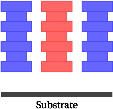
55 Matching passives Systematic vs. random Different absolute values between runs Layout dependent problems Stress, thermal, or doping gradients Good layout practice helps Unit elements Dummies (each unit element should see the exact same surroundings) Interdigitation or common centroid


56 Unit elements Instead, make identical unit elements. Less systematic mismatch.


57 Dummy elements Dummies to make sure matching elements see the same surroundings


58 Interdigitated layout Process gradient are spread more evenly between the two elements. Proximity helps with matching!


59 Common centroid Better process gradient cancelation than interdigitated layout. Perfect cancelation of linear gradients.
60 Drawing transistors Unit elements, dummy, and common centroid also applies to layout of transistors. However, there are additional issues that need attention when laying out transistors. Multi-finger devices S/D symmetry WPE and LOD Latch-up
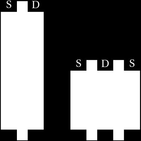
61 Multi-finger devices


62 Device orientation Devices with different orientation do not match!


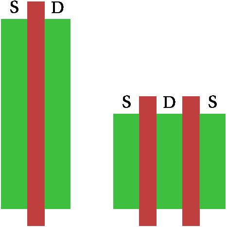
63 Source/drain asymmetry Source and drain may not be symmetric due to ion implantation angle, neccessary to avoid implant depth issues (channeling).
64 Well proximity effect High energy ion implants to form the well. Scattering from the edge of the photoresist mask, and embedding in the silicon surface (near well edge). Transistors close to the well edge will therefore have different properties. This is known as the well proximity effect (WPE). Important for matching.


65 Well proximity effect As with S/D, implantation angle may render the scattering and doping asymmetric
66 STI stress (LOD) Shallow trench isolation strains the active area of the transistor. Influcences mobility and threshold voltage (stress induced enhancement or suppression of dopant diffusion). Distance between gate and STI impacts perfomance. Important for matching. (Parameters SA and SB in BSIM). Also known as LOD (length of diffusion), LOD = SA + SB + L


67 STI stress (LOD)


68 Transistor interconnect Unbalanced metal routing will cause the transistors to see different source voltage. Also, distribute reference as current, not bias voltage.
69 Matching This discussion about matching was about minimizing systematic mismatch. We will discuss random mismatch later.
70 Shielding Substrate ties circuits together. Digital switching couples to the substrate. Guard rings around the circuit: Substrate ties and n-well (preferably deep n-well) Separate Vdd for digital and analog Fully differential signals See sect in Razavi's book.
71 Latch-up As we saw with bandgap references. Parasitic BJTs are readily available in CMOS. Parasitic BJTs may inadvertently turn on due to a large injection of current into the substrate. Typical design rules make sure that substrate and n-well contacts have sufficiently small spacing. However, latchup is an important problem, and requires careful consideration.
72 Bond pads Used for connecting bond wires between die and package. Mechanical stability ESD protection (very important, and adds C) Aluminum (while other metal is Cu) Pad frame usually contains supply nets (also used by ESD circuitry)

73 Bond pads Bonding gone wrong...
74 Seal ring A seal ring is a structure to enclose the die (outside the pad frame). Protects the die from moisture and sawing. Also contains scribe (where to saw the die).
75 Packaging Packaging adds very significant parasitics. Bond wires introduce inductance. Rule of thumb is 1 nh/mm. Inductors like to keep current constant. Voltage will change to make this happen. Important to balance with decoupling capacitors. However, transients will remain.
76 References Hastings, The Art of Analog Layout, Prentice Hall, 2001 Orshansky, et al., Design for Manufacturability and Statistical Design, Springer, 2008 Wong, et al., Nano-CMOS Circuit and Physical Design, Wiley, 2005
Layout and technology
 INF4420 Layout and technology Dag T. Wisland Spring 2015 Outline CMOS technology Design rules Analog layout Mismatch Spring 2015 Layout and technology 2 Introduction As circuit designers we must carefully
Outline. Layout and technology. CMOS technology Design rules Analog layout Mismatch INF4420. Jørgen Andreas Michaelsen Spring / 80 2 / 80
 INF4420 Layout and technology Jørgen Andreas Michaelsen Spring 2013 1 / 80 Outline CMOS technology Design rules Analog layout Mismatch Spring 2013 Layout and technology 2 2 / 80 Introduction As circuit
INF4420 Lecture Notes
 INF4420 Lecture Notes Jørgen Andreas Michaelsen (jorgenam@ifi.uio.no) Spring 2012 INF4420 Introduction Spring 2012 1 / 32 Outline Practical information about the course. Context (placing what we will
Topic 3. CMOS Fabrication Process
 Topic 3 CMOS Fabrication Process Peter Cheung Department of Electrical & Electronic Engineering Imperial College London URL: www.ee.ic.ac.uk/pcheung/ E-mail: p.cheung@ic.ac.uk Lecture 3-1 Layout of a Inverter
Fabrication, Corner, Layout, Matching, & etc.
 Advanced Analog Building Blocks Fabrication, Corner, Layout, Matching, & etc. Wei SHEN (KIP) 1 Fabrication Steps for MOS Wei SHEN, Universität Heidelberg 2 Fabrication Steps for MOS Wei SHEN, Universität
Lecture 020 ECE4430 Review II (1/5/04) Page 020-1
 Page 020-1") Lecture 020 ECE4430 Review II (1/5/04) Page 020-1 LECTURE 020 ECE 4430 REVIEW II (READING: GHLM - Chap. 2) Objective The objective of this presentation is: 1.) Identify the prerequisite material as taught
Lecture 020 ECE4430 Review II (1/5/04) Page 020-1 LECTURE 020 ECE 4430 REVIEW II (READING: GHLM - Chap. 2) Objective The objective of this presentation is: 1.) Identify the prerequisite material as taught
Jack Keil Wolf Lecture. ESE 570: Digital Integrated Circuits and VLSI Fundamentals. Lecture Outline. MOSFET N-Type, P-Type.
 ESE 570: Digital Integrated Circuits and VLSI Fundamentals Jack Keil Wolf Lecture Lec 3: January 24, 2019 MOS Fabrication pt. 2: Design Rules and Layout http://www.ese.upenn.edu/about-ese/events/wolf.php
Layout of a Inverter. Topic 3. CMOS Fabrication Process. The CMOS Process - photolithography (2) The CMOS Process - photolithography (1) v o.
 The CMOS Process - photolithography (1) v o.") Layout of a Inverter Topic 3 CMOS Fabrication Process V DD Q p Peter Cheung Department of Electrical & Electronic Engineering Imperial College London v i v o Q n URL: www.ee.ic.ac.uk/pcheung/ E-mail: p.cheung@ic.ac.uk
Layout of a Inverter Topic 3 CMOS Fabrication Process V DD Q p Peter Cheung Department of Electrical & Electronic Engineering Imperial College London v i v o Q n URL: www.ee.ic.ac.uk/pcheung/ E-mail: p.cheung@ic.ac.uk
Advanced Digital Integrated Circuits. Lecture 2: Scaling Trends. Announcements. No office hour next Monday. Extra office hour Tuesday 2-3pm
 EE241 - Spring 20 Advanced Digital Integrated Circuits Lecture 2: Scaling Trends and Features of Modern Technologies Announcements No office hour next Monday Extra office hour Tuesday 2-3pm 2 1 Outline
ESE 570: Digital Integrated Circuits and VLSI Fundamentals
 ESE 570: Digital Integrated Circuits and VLSI Fundamentals Lec 3: January 24, 2019 MOS Fabrication pt. 2: Design Rules and Layout Penn ESE 570 Spring 2019 Khanna Jack Keil Wolf Lecture http://www.ese.upenn.edu/about-ese/events/wolf.php
ECE 5745 Complex Digital ASIC Design Topic 2: CMOS Devices
 ECE 5745 Complex Digital ASIC Design Topic 2: CMOS Devices Christopher Batten School of Electrical and Computer Engineering Cornell University http://www.csl.cornell.edu/courses/ece5950 Simple Transistor
Bridging the Gap between Dreams and Nano-Scale Reality
 Bridging the Gap between Dreams and Nano-Scale Reality Ban P. Wong Design Methodology, Chartered Semiconductor wongb@charteredsemi.com 28 July 2006 Outline Deficiencies in Boolean-based Design Rules in
The Art of ANALOG LAYOUT Second Edition
 The Art of ANALOG LAYOUT Second Edition Alan Hastings 3 EARSON Pearson Education International Contents Preface to the Second Edition xvii Preface to the First Edition xix Acknowledgments xxi 1 Device
Variation-Aware Design for Nanometer Generation LSI
 HIRATA Morihisa, SHIMIZU Takashi, YAMADA Kenta Abstract Advancement in the microfabrication of semiconductor chips has made the variations and layout-dependent fluctuations of transistor characteristics
Modeling and CAD Challenges for DFY. Patrick G. Drennan Freescale Semiconductor Tempe, AZ, USA
 Modeling and CAD Challenges for DFY Patrick G. Drennan Freescale Semiconductor Tempe, AZ, USA Outline Unphysical casing and statistical models Process gradients Gate protect diodes Shallow trench isolation
2.8 - CMOS TECHNOLOGY
 CMOS Technology (6/7/00) Page 1 2.8 - CMOS TECHNOLOGY INTRODUCTION Objective The objective of this presentation is: 1.) Illustrate the fabrication sequence for a typical MOS transistor 2.) Show the physical
CMOS Digital Integrated Circuits Lec 2 Fabrication of MOSFETs
 CMOS Digital Integrated Circuits Lec 2 Fabrication of MOSFETs 1 CMOS Digital Integrated Circuits 3 rd Edition Categories of Materials Materials can be categorized into three main groups regarding their
Processing and Reliability Issues That Impact Design Practice. Overview
 Lecture 15 Processing and Reliability Issues That Impact Design Practice Zongjian Chen Zongjian_chen@yahoo.com Copyright 2004 by Zongjian Chen 1 Overview As a maturing industry, semiconductor food chain
EE241 - Spring 2013 Advanced Digital Integrated Circuits. Announcements. Sign up for Piazza if you haven t already
 EE241 - Spring 2013 Advanced Digital Integrated Circuits Lecture 2: Scaling Trends and Features of Modern Technologies Announcements Sign up for Piazza if you haven t already 2 1 Assigned Reading R.H.
Session 3: Solid State Devices. Silicon on Insulator
 Session 3: Solid State Devices Silicon on Insulator 1 Outline A B C D E F G H I J 2 Outline Ref: Taurand Ning 3 SOI Technology SOl materials: SIMOX, BESOl, and Smart Cut SIMOX : Synthesis by IMplanted
Basic Fabrication Steps
 Basic Fabrication Steps and Layout Somayyeh Koohi Department of Computer Engineering Adapted with modifications from lecture notes prepared by author Outline Fabrication steps Transistor structures Transistor
Newer process technology (since 1999) includes :
 includes :") Newer process technology (since 1999) includes : copper metalization hi-k dielectrics for gate insulators si on insulator strained silicon lo-k dielectrics for interconnects Immersion lithography for masks
Newer process technology (since 1999) includes : copper metalization hi-k dielectrics for gate insulators si on insulator strained silicon lo-k dielectrics for interconnects Immersion lithography for masks
Photolithography I ( Part 1 )
") 1 Photolithography I ( Part 1 ) Chapter 13 : Semiconductor Manufacturing Technology by M. Quirk & J. Serda Bjørn-Ove Fimland, Department of Electronics and Telecommunication, Norwegian University of Science
1 Photolithography I ( Part 1 ) Chapter 13 : Semiconductor Manufacturing Technology by M. Quirk & J. Serda Bjørn-Ove Fimland, Department of Electronics and Telecommunication, Norwegian University of Science
Microelectronics, BSc course
 Microelectronics, BSc course MOS circuits: CMOS circuits, construction http://www.eet.bme.hu/~poppe/miel/en/14-cmos.pptx http://www.eet.bme.hu The abstraction level of our study: SYSTEM + MODULE GATE CIRCUIT
Chapter 3: Basics Semiconductor Devices and Processing 2006/9/27 1. Topics
 Chapter 3: Basics Semiconductor Devices and Processing 2006/9/27 1 Topics What is semiconductor Basic semiconductor devices Basics of IC processing CMOS technologies 2006/9/27 2 1 What is Semiconductor
Prepared by Dr. Ulkuhan Guler GT-Bionics Lab Georgia Institute of Technology
 Prepared by Dr. Ulkuhan Guler GT-Bionics Lab Georgia Institute of Technology OUTLINE Understanding Fabrication Imperfections Layout of MOS Transistor Matching Theory and Mismatches Device Matching, Interdigitation
1 FUNDAMENTAL CONCEPTS What is Noise Coupling 1
 Contents 1 FUNDAMENTAL CONCEPTS 1 1.1 What is Noise Coupling 1 1.2 Resistance 3 1.2.1 Resistivity and Resistance 3 1.2.2 Wire Resistance 4 1.2.3 Sheet Resistance 5 1.2.4 Skin Effect 6 1.2.5 Resistance
! Review: MOS IV Curves and Switch Model. ! MOS Device Layout. ! Inverter Layout. ! Gate Layout and Stick Diagrams. ! Design Rules. !
 ESE 570: Digital Integrated Circuits and VLSI Fundamentals Lec 3: January 21, 2017 MOS Fabrication pt. 2: Design Rules and Layout Lecture Outline! Review: MOS IV Curves and Switch Model! MOS Device Layout!
Chapter 3 Basics Semiconductor Devices and Processing
 Chapter 3 Basics Semiconductor Devices and Processing 1 Objectives Identify at least two semiconductor materials from the periodic table of elements List n-type and p-type dopants Describe a diode and
FABRICATION OF CMOS INTEGRATED CIRCUITS. Dr. Mohammed M. Farag
 FABRICATION OF CMOS INTEGRATED CIRCUITS Dr. Mohammed M. Farag Outline Overview of CMOS Fabrication Processes The CMOS Fabrication Process Flow Design Rules Reference: Uyemura, John P. "Introduction to
EE 5611 Introduction to Microelectronic Technologies Fall Thursday, September 04, 2014 Lecture 02
 EE 5611 Introduction to Microelectronic Technologies Fall 2014 Thursday, September 04, 2014 Lecture 02 1 Lecture Outline Review on semiconductor materials Review on microelectronic devices Example of microelectronic
! Review: MOS IV Curves and Switch Model. ! MOS Device Layout. ! Inverter Layout. ! Gate Layout and Stick Diagrams. ! Design Rules. !
 ESE 570: Digital Integrated Circuits and VLSI Fundamentals Lec 3: January 21, 2016 MOS Fabrication pt. 2: Design Rules and Layout Lecture Outline! Review: MOS IV Curves and Switch Model! MOS Device Layout!
ESE 570: Digital Integrated Circuits and VLSI Fundamentals
 ESE 570: Digital Integrated Circuits and VLSI Fundamentals Lec 3: January 21, 2016 MOS Fabrication pt. 2: Design Rules and Layout Penn ESE 570 Spring 2016 Khanna Adapted from GATech ESE3060 Slides Lecture
Fin-Shaped Field Effect Transistor (FinFET) Min Ku Kim 03/07/2018
 Min Ku Kim 03/07/2018") Fin-Shaped Field Effect Transistor (FinFET) Min Ku Kim 03/07/2018 ECE 658 Sp 2018 Semiconductor Materials and Device Characterizations OUTLINE Background FinFET Future Roadmap Keeping up w/ Moore s Law
Fin-Shaped Field Effect Transistor (FinFET) Min Ku Kim 03/07/2018 ECE 658 Sp 2018 Semiconductor Materials and Device Characterizations OUTLINE Background FinFET Future Roadmap Keeping up w/ Moore s Law
Fundamentals of Power Semiconductor Devices
 В. Jayant Baliga Fundamentals of Power Semiconductor Devices 4y Spri ringer Contents Preface vii Chapter 1 Introduction 1 1.1 Ideal and Typical Power Switching Waveforms 3 1.2 Ideal and Typical Power Device
Basic Functional Analysis. Sample Report Richmond Road, Suite 500, Ottawa, ON K2H 5B7 Canada Tel:
 Basic Functional Analysis Sample Report 3685 Richmond Road, Suite 500, Ottawa, ON K2H 5B7 Canada Tel: 613-829-0414 www.chipworks.com Basic Functional Analysis Sample Report Some of the information in this
DATASHEET CADENCE QRC EXTRACTION
 DATASHEET Cadence QRC Etraction, the industry s premier 3D fullchip parasitic etractor that is independent of design style or flow, is a fast and accurate RLCK etraction solution used during design implementation
(a) (d) (e) (b) (c) (f) 3D-NAND Flash and Its Manufacturing Process
 (d) (e) (b) (c) (f) 3D-NAND Flash and Its Manufacturing Process") 3D-NAND Flash and Its Manufacturing Process 79 (d) Si Si (b) (c) (e) Si (f) +1-2 (g) (h) Figure 2.33 Top-down view in cap oxide and (b) in nitride_n-2; (c) cross-section near the top of the channel; top-down
3D-NAND Flash and Its Manufacturing Process 79 (d) Si Si (b) (c) (e) Si (f) +1-2 (g) (h) Figure 2.33 Top-down view in cap oxide and (b) in nitride_n-2; (c) cross-section near the top of the channel; top-down
Integrated diodes. The forward voltage drop only slightly depends on the forward current. ELEKTRONIKOS ĮTAISAI
 1 Integrated diodes pn junctions of transistor structures can be used as integrated diodes. The choice of the junction is limited by the considerations of switching speed and breakdown voltage. The forward
Notes. (Subject Code: 7EC5)
") COMPUCOM INSTITUTE OF TECHNOLOGY & MANAGEMENT, JAIPUR (DEPARTMENT OF ELECTRONICS & COMMUNICATION) Notes VLSI DESIGN NOTES (Subject Code: 7EC5) Prepared By: MANVENDRA SINGH Class: B. Tech. IV Year, VII
COMPUCOM INSTITUTE OF TECHNOLOGY & MANAGEMENT, JAIPUR (DEPARTMENT OF ELECTRONICS & COMMUNICATION) Notes VLSI DESIGN NOTES (Subject Code: 7EC5) Prepared By: MANVENDRA SINGH Class: B. Tech. IV Year, VII
Lecture 04 CSE 40547/60547 Computing at the Nanoscale Interconnect
 Lecture 04 CSE 40547/60547 Computing at the Nanoscale Interconnect Introduction - So far, have considered transistor-based logic in the face of technology scaling - Interconnect effects are also of concern
CMOS: Fabrication principles and design rules
 CMOS: Fabrication principles and design rules João Canas Ferreira University of Porto Faculty of Engineering 2016-02-29 Topics 1 Overview of the CMOS fabrication process 2 Geometric design rules João Canas
Semiconductor Physics and Devices
 Metal-Semiconductor and Semiconductor Heterojunctions The Metal-Oxide-Semiconductor Field-Effect Transistor (MOSFET) is one of two major types of transistors. The MOSFET is used in digital circuit, because
Lithography. 3 rd. lecture: introduction. Prof. Yosi Shacham-Diamand. Fall 2004
 Lithography 3 rd lecture: introduction Prof. Yosi Shacham-Diamand Fall 2004 1 List of content Fundamental principles Characteristics parameters Exposure systems 2 Fundamental principles Aerial Image Exposure
Mechanis m Faliures. Group Leader Jepsy 1)Substrate Biasing 2) Minority Injection. Bob 1)Minority-Carrier Guard Rings
Substrate Biasing 2) Minority Injection. Bob 1)Minority-Carrier Guard Rings") Mechanis m Faliures Group Leader Jepsy 1)Substrate Biasing 2) Minority Injection As im 1)Types Of Guard Rings Sandra 1)Parasitics 2)Field Plating Bob 1)Minority-Carrier Guard Rings Shawn 1)Parasitic Channel
Mechanis m Faliures Group Leader Jepsy 1)Substrate Biasing 2) Minority Injection As im 1)Types Of Guard Rings Sandra 1)Parasitics 2)Field Plating Bob 1)Minority-Carrier Guard Rings Shawn 1)Parasitic Channel
IFSIN. WEB PAGE Fall ://weble.upc.es/ifsin/
 IFSIN IMPLEMENTACIÓ FÍSICA DE SISTEMES INTEGRATS NANOMÈTRICS IMPLEMENTACIÓN N FÍSICA F DE SISTEMAS INTEGRADOS NANOMÉTRICOS PHYSICAL IMPLEMENTATION OF NANOMETER INTEGRATED SYSTEMS Fall 2008 Prof. Xavier
Lecture 0: Introduction
 Lecture 0: Introduction Introduction Integrated circuits: many transistors on one chip. Very Large Scale Integration (VLSI): bucketloads! Complementary Metal Oxide Semiconductor Fast, cheap, low power
45nm Foundry CMOS with Mask-Lite Reduced Mask Costs
 This work is sponsored by the Air Force Research Laboratory (AFRL/RVSE) TPOC: Mr. Kenneth Hebert 45nm Foundry CMOS with Mask-Lite Reduced Mask Costs 25 October 2011 www.americansemi.com 2011 American Semiconductor,
3084 IEEE TRANSACTIONS ON NUCLEAR SCIENCE, VOL. 60, NO. 4, AUGUST 2013
 3084 IEEE TRANSACTIONS ON NUCLEAR SCIENCE, VOL. 60, NO. 4, AUGUST 2013 Dummy Gate-Assisted n-mosfet Layout for a Radiation-Tolerant Integrated Circuit Min Su Lee and Hee Chul Lee Abstract A dummy gate-assisted
Lecture: Integration of silicon photonics with electronics. Prepared by Jean-Marc FEDELI CEA-LETI
 Lecture: Integration of silicon photonics with electronics Prepared by Jean-Marc FEDELI CEA-LETI Context The goal is to give optical functionalities to electronics integrated circuit (EIC) The objectives
Maxim MAX3940E Electro-Absorption Modulator Structural Analysis
 May 23, 2006 Maxim MAX3940E Electro-Absorption Modulator Structural Analysis For comments, questions, or more information about this report, or for any additional technical needs concerning semiconductor
Transistor was first invented by William.B.Shockley, Walter Brattain and John Bardeen of Bell Labratories. In 1961, first IC was introduced.
 Unit 1 Basic MOS Technology Transistor was first invented by William.B.Shockley, Walter Brattain and John Bardeen of Bell Labratories. In 1961, first IC was introduced. Levels of Integration:- i) SSI:-
FUTURE PROSPECTS FOR CMOS ACTIVE PIXEL SENSORS
 FUTURE PROSPECTS FOR CMOS ACTIVE PIXEL SENSORS Dr. Eric R. Fossum Jet Propulsion Laboratory Dr. Philip H-S. Wong IBM Research 1995 IEEE Workshop on CCDs and Advanced Image Sensors April 21, 1995 CMOS APS
Chapter 15 Summary and Future Trends
 Chapter 15 Summary and Future Trends Hong Xiao, Ph. D. hxiao89@hotmail.com www2.austin.cc.tx.us/hongxiao/book.htm Hong Xiao, Ph. D. www2.austin.cc.tx.us/hongxiao/book.htm 1 The 1960s First IC product Bipolar
! MOS Device Layout. ! Inverter Layout. ! Gate Layout and Stick Diagrams. ! Design Rules. ! Standard Cells. ! CMOS Process Enhancements
 EE 570: igital Integrated Circuits and VLI Fundamentals Lec 3: January 18, 2018 MO Fabrication pt. 2: esign Rules and Layout Lecture Outline! MO evice Layout! Inverter Layout! Gate Layout and tick iagrams!
Key Questions. ECE 340 Lecture 39 : Introduction to the BJT-II 4/28/14. Class Outline: Fabrication of BJTs BJT Operation
 Things you should know when you leave ECE 340 Lecture 39 : Introduction to the BJT-II Fabrication of BJTs Class Outline: Key Questions What elements make up the base current? What do the carrier distributions
INTRODUCTION: Basic operating principle of a MOSFET:
 INTRODUCTION: Along with the Junction Field Effect Transistor (JFET), there is another type of Field Effect Transistor available whose Gate input is electrically insulated from the main current carrying
Semiconductor Devices
 Semiconductor Devices - 2014 Lecture Course Part of SS Module PY4P03 Dr. P. Stamenov School of Physics and CRANN, Trinity College, Dublin 2, Ireland Hilary Term, TCD 3 th of Feb 14 MOSFET Unmodified Channel
State-of-the-art device fabrication techniques
 State-of-the-art device fabrication techniques! Standard Photo-lithography and e-beam lithography! Advanced lithography techniques used in semiconductor industry Deposition: Thermal evaporation, e-gun
Section 2: Lithography. Jaeger Chapter 2 Litho Reader. The lithographic process
 Section 2: Lithography Jaeger Chapter 2 Litho Reader The lithographic process Photolithographic Process (a) (b) (c) (d) (e) (f) (g) Substrate covered with silicon dioxide barrier layer Positive photoresist
6.776 High Speed Communication Circuits Lecture 6 MOS Transistors, Passive Components, Gain- Bandwidth Issue for Broadband Amplifiers
 6.776 High Speed Communication Circuits Lecture 6 MOS Transistors, Passive Components, Gain- Bandwidth Issue for Broadband Amplifiers Massachusetts Institute of Technology February 17, 2005 Copyright 2005
SAMPLE SLIDES & COURSE OUTLINE. Core Competency In Semiconductor Technology: 2. FABRICATION. Dr. Theodore (Ted) Dellin
 Dellin") & Digging Deeper Devices, Fabrication & Reliability For More Info:.com or email Dellin@ieee.org SAMPLE SLIDES & COURSE OUTLINE In : 2. A Easy, Effective, of How Devices Are.. Recommended for everyone who
& Digging Deeper Devices, Fabrication & Reliability For More Info:.com or email Dellin@ieee.org SAMPLE SLIDES & COURSE OUTLINE In : 2. A Easy, Effective, of How Devices Are.. Recommended for everyone who
420 Intro to VLSI Design
 Dept of Electrical and Computer Engineering 420 Intro to VLSI Design Lecture 0: Course Introduction and Overview Valencia M. Joyner Spring 2005 Getting Started Syllabus About the Instructor Labs, Problem
Section 2: Lithography. Jaeger Chapter 2. EE143 Ali Javey Slide 5-1
 Section 2: Lithography Jaeger Chapter 2 EE143 Ali Javey Slide 5-1 The lithographic process EE143 Ali Javey Slide 5-2 Photolithographic Process (a) (b) (c) (d) (e) (f) (g) Substrate covered with silicon
BCD Smart Power Roadmap Trends and Challenges. Giuseppe Croce NEREID WORKSHOP Smart Energy Bertinoro, October 20 th
 BCD Smart Power Roadmap Trends and Challenges Giuseppe Croce NEREID WORKSHOP Smart Energy Bertinoro, October 20 th Outline 2 Introduction Major Trends in Smart Power ASICs An insight on (some) differentiating
Section 2: Lithography. Jaeger Chapter 2 Litho Reader. EE143 Ali Javey Slide 5-1
 Section 2: Lithography Jaeger Chapter 2 Litho Reader EE143 Ali Javey Slide 5-1 The lithographic process EE143 Ali Javey Slide 5-2 Photolithographic Process (a) (b) (c) (d) (e) (f) (g) Substrate covered
Wiring Parasitics. Contact Resistance Measurement and Rules
 Wiring Parasitics Contact Resistance Measurement and Rules Connections between metal layers and nonmetal layers are called contacts. Connections between metal layers are called vias. For non-critical design,
Conduction Characteristics of MOS Transistors (for fixed Vds)! Topic 2. Basic MOS theory & SPICE simulation. MOS Transistor
! Topic 2. Basic MOS theory & SPICE simulation. MOS Transistor") Conduction Characteristics of MOS Transistors (for fixed Vds)! Topic 2 Basic MOS theory & SPICE simulation Peter Cheung Department of Electrical & Electronic Engineering Imperial College London (Weste&Harris,
Conduction Characteristics of MOS Transistors (for fixed Vds)! Topic 2 Basic MOS theory & SPICE simulation Peter Cheung Department of Electrical & Electronic Engineering Imperial College London (Weste&Harris,
Topic 2. Basic MOS theory & SPICE simulation
 Topic 2 Basic MOS theory & SPICE simulation Peter Cheung Department of Electrical & Electronic Engineering Imperial College London (Weste&Harris, Ch 2 & 5.1-5.3 Rabaey, Ch 3) URL: www.ee.ic.ac.uk/pcheung/
Conduction Characteristics of MOS Transistors (for fixed Vds) Topic 2. Basic MOS theory & SPICE simulation. MOS Transistor
 Topic 2. Basic MOS theory & SPICE simulation. MOS Transistor") Conduction Characteristics of MOS Transistors (for fixed Vds) Topic 2 Basic MOS theory & SPICE simulation Peter Cheung Department of Electrical & Electronic Engineering Imperial College London (Weste&Harris,
Conduction Characteristics of MOS Transistors (for fixed Vds) Topic 2 Basic MOS theory & SPICE simulation Peter Cheung Department of Electrical & Electronic Engineering Imperial College London (Weste&Harris,
MITLL Low-Power FDSOI CMOS Process
 MITLL Low-Power FDSOI CMOS Process Application Notes Revision 2006:1 (June 2006) 2006 by MIT Lincoln Laboratory. All rights reserved. This work was sponsored by the United States Air Force under Air Force
EE4800 CMOS Digital IC Design & Analysis. Lecture 1 Introduction Zhuo Feng
 EE4800 CMOS Digital IC Design & Analysis Lecture 1 Introduction Zhuo Feng 1.1 Prof. Zhuo Feng Office: EERC 730 Phone: 487-3116 Email: zhuofeng@mtu.edu Class Website http://www.ece.mtu.edu/~zhuofeng/ee4800fall2010.html
Fundamentals of Integrated Circuit Design
 1. Definitions Integrated circuits Fundamentals of Integrated Circuit Design An integrated circuit (IC) is formed by components and interconnections that are fabricated on a single silicon piece of semiconductor,
ECE520 VLSI Design. Lecture 2: Basic MOS Physics. Payman Zarkesh-Ha
 ECE520 VLSI Design Lecture 2: Basic MOS Physics Payman Zarkesh-Ha Office: ECE Bldg. 230B Office hours: Wednesday 2:00-3:00PM or by appointment E-mail: pzarkesh@unm.edu Slide: 1 Review of Last Lecture Semiconductor
VLSI Technology Dr. Nandita Dasgupta Department of Electrical Engineering Indian Institute of Technology, Madras
 VLSI Technology Dr. Nandita Dasgupta Department of Electrical Engineering Indian Institute of Technology, Madras Lecture - 40 BICMOS technology So, today we are going to have the last class on this VLSI
Design Simulation and Analysis of NMOS Characteristics for Varying Oxide Thickness
 MIT International Journal of Electronics and Communication Engineering, Vol. 4, No. 2, August 2014, pp. 81 85 81 Design Simulation and Analysis of NMOS Characteristics for Varying Oxide Thickness Alpana
+1 (479)
") Introduction to VLSI Design http://csce.uark.edu +1 (479) 575-6043 yrpeng@uark.edu Invention of the Transistor Vacuum tubes ruled in first half of 20th century Large, expensive, power-hungry, unreliable
Introduction to VLSI Design http://csce.uark.edu +1 (479) 575-6043 yrpeng@uark.edu Invention of the Transistor Vacuum tubes ruled in first half of 20th century Large, expensive, power-hungry, unreliable
Major Fabrication Steps in MOS Process Flow
 Major Fabrication Steps in MOS Process Flow UV light Mask oxygen Silicon dioxide photoresist exposed photoresist oxide Silicon substrate Oxidation (Field oxide) Photoresist Coating Mask-Wafer Alignment
EE 330 Lecture 7. Design Rules. IC Fabrication Technology Part 1
 EE 330 Lecture 7 Design Rules IC Fabrication Technology Part 1 Review from Last Time Technology Files Provide Information About Process Process Flow (Fabrication Technology) Model Parameters Design Rules
Power MOSFET Zheng Yang (ERF 3017,
 ECE442 Power Semiconductor Devices and Integrated Circuits Power MOSFET Zheng Yang (ERF 3017, email: yangzhen@uic.edu) Evolution of low-voltage (
Alternatives to standard MOSFETs. What problems are we really trying to solve?
 Alternatives to standard MOSFETs A number of alternative FET schemes have been proposed, with an eye toward scaling up to the 10 nm node. Modifications to the standard MOSFET include: Silicon-in-insulator
Intel Xeon E3-1230V2 CPU Ivy Bridge Tri-Gate 22 nm Process
 Intel Xeon E3-1230V2 CPU Structural Analysis 3685 Richmond Road, Suite 500, Ottawa, ON K2H 5B7 Canada Tel: 613-829-0414 www.chipworks.com Structural Analysis Some of the information in this report may
UNIT-VI FIELD EFFECT TRANSISTOR. 1. Explain about the Field Effect Transistor and also mention types of FET s.
 UNIT-I FIELD EFFECT TRANSISTOR 1. Explain about the Field Effect Transistor and also mention types of FET s. The Field Effect Transistor, or simply FET however, uses the voltage that is applied to their
Phase Locked Loops, Report Writing, Layout Tuesday, April 5th, 9:15 11:00
 Phase Locked Loops, Report Writing, Layout Tuesday, April 5th, 9:15 11:00 Snorre Aunet (sa@ifi.uio.no) Nanoelectronics group Department of Informatics University of Oslo Last time and today, Tuesday 5th
Samsung S5K3BAFB 2 Megapixel CMOS Image Sensor 0.13 µm Copper CMOS Process Process Review Report
 October 13, 2006 Samsung S5K3BAFB 2 Megapixel CMOS Image Sensor 0.13 µm Copper CMOS Process Process Review Report (with Optional TEM Analysis) For comments, questions, or more information about this report,
Design of Analog CMOS Integrated Circuits
 Design of Analog CMOS Integrated Circuits Behzad Razavi Professor of Electrical Engineering University of California, Los Angeles H Boston Burr Ridge, IL Dubuque, IA Madison, WI New York San Francisco
Broadcom BCM43224KMLG Baseband/MAC/Radio All-in-One Die SMIC 65 nm Process
 Broadcom BCM43224KMLG Baseband/MAC/Radio All-in-One Die SMIC 65 nm Process Structural Analysis 1891 Robertson Road, Suite 500, Ottawa, ON K2H 5B7 Canada Tel: 613-829-0414 www.chipworks.com Structural Analysis
Semiconductor Memory: DRAM and SRAM. Department of Electrical and Computer Engineering, National University of Singapore
 Semiconductor Memory: DRAM and SRAM Outline Introduction Random Access Memory (RAM) DRAM SRAM Non-volatile memory UV EPROM EEPROM Flash memory SONOS memory QD memory Introduction Slow memories Magnetic
FinFET vs. FD-SOI Key Advantages & Disadvantages
 FinFET vs. FD-SOI Key Advantages & Disadvantages Amiad Conley Technical Marketing Manager Process Diagnostics & Control, Applied Materials ChipEx-2014, Apr 2014 1 Moore s Law The number of transistors
ECE 340 Lecture 37 : Metal- Insulator-Semiconductor FET Class Outline:
 ECE 340 Lecture 37 : Metal- Insulator-Semiconductor FET Class Outline: Metal-Semiconductor Junctions MOSFET Basic Operation MOS Capacitor Things you should know when you leave Key Questions What is the
5. Lithography. 1. photolithography intro: overall, clean room 2. principle 3. tools 4. pattern transfer 5. resolution 6. next-gen
 5. Lithography 1. photolithography intro: overall, clean room 2. principle 3. tools 4. pattern transfer 5. resolution 6. next-gen References: Semiconductor Devices: Physics and Technology. 2 nd Ed. SM
Lecture #29. Moore s Law
 Lecture #29 ANNOUNCEMENTS HW#15 will be for extra credit Quiz #6 (Thursday 5/8) will include MOSFET C-V No late Projects will be accepted after Thursday 5/8 The last Coffee Hour will be held this Thursday
EECS130 Integrated Circuit Devices
 EECS130 Integrated Circuit Devices Professor Ali Javey 11/6/2007 MOSFETs Lecture 6 BJTs- Lecture 1 Reading Assignment: Chapter 10 More Scalable Device Structures Vertical Scaling is important. For example,
Rockchip RK3188 Mobile Application Processor GF 28 nm SLP Gate First HKMG CMOS Process
 Rockchip RK3188 Mobile Application Processor GF 28 nm SLP Gate First HKMG CMOS Process Process Review FEOL Analysis 1891 Robertson Road, Suite 500, Ottawa, ON K2H 5B7 Canada Tel: 613-829-0414 www.chipworks.com
ECSE-6300 IC Fabrication Laboratory Lecture 9 MOSFETs. Lecture Outline
 ECSE-6300 IC Fabrication Laboratory Lecture 9 MOSFETs Prof. Rensselaer Polytechnic Institute Troy, NY 12180 Office: CII-6229 Tel.: (518) 276-2909 e-mails: luj@rpi.edu http://www.ecse.rpi.edu/courses/s18/ecse
AE53/AC53/AT53/AE103 ELECT. DEVICES & CIRCUITS DEC 2015
 Q.2 a. By using Norton s theorem, find the current in the load resistor R L for the circuit shown in Fig.1. (8) Fig.1 IETE 1 b. Explain Z parameters and also draw an equivalent circuit of the Z parameter
TECHNO INDIA BATANAGAR (DEPARTMENT OF ELECTRONICS & COMMUNICATION ENGINEERING) QUESTION BANK- 2018
 QUESTION BANK- 2018") TECHNO INDIA BATANAGAR (DEPARTMENT OF ELECTRONICS & COMMUNICATION ENGINEERING) QUESTION BANK- 2018 Paper Setter Detail Name Designation Mobile No. E-mail ID Raina Modak Assistant Professor 6290025725 raina.modak@tib.edu.in
TECHNO INDIA BATANAGAR (DEPARTMENT OF ELECTRONICS & COMMUNICATION ENGINEERING) QUESTION BANK- 2018 Paper Setter Detail Name Designation Mobile No. E-mail ID Raina Modak Assistant Professor 6290025725 raina.modak@tib.edu.in
First Results of 0.15μm CMOS SOI Pixel Detector
 First Results of 0.15μm CMOS SOI Pixel Detector International Symposium on Detector Development SLAC, CA, April 5, 2006 KEK Detector Technology Project : [SOIPIX Group] Yasuo Arai (KEK) Y. Arai Y. Ikegami
Signal Integrity Design of TSV-Based 3D IC
 Signal Integrity Design of TSV-Based 3D IC October 24, 21 Joungho Kim at KAIST joungho@ee.kaist.ac.kr http://tera.kaist.ac.kr 1 Contents 1) Driving Forces of TSV based 3D IC 2) Signal Integrity Issues