CMOS 65nm Process Monitor
|
|
|
- Adam Terry
- 5 years ago
- Views:
Transcription
1 CMOS 65nm Process Monitor Advisors: Dr. Hugh Grinolds Mr. Brian Misek Allen Chen Ryan Hoppal Phillip Misek
2 What is Process Variation? The process parameters can vary from: Lot-to-Lot (interprocess variation) Wafer-to-wafer (interprocess variation) Die-to-die (intraprocess) Variations in process parameters include: Doping densities Oxide thickness Diffusion depths W and L of transistors These variations are strongly correlated so it s difficult to isolate individual parameters
3 I dsat PMOS Die-to-Die Variation SF FF Spec SS Typ. FS SkewTarget W1 Courtesy: Brian Misek I dsat NMOS

4 Variations on a Wafer Frequency Fast Failed Slow Mid
5 Design Flow Modeling Layout Extraction Final Design
")
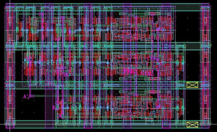
6 Layout (Cadence) NAND
7 Our Process Monitor On-die 65nm process compatible Selector Block Inverter Delay Module Poly Resistance Module Future Expansion Output Register
8 Our Design Constraints Requirements: Size: < 100um x 100um per module Power-down mode Digital Output one 8-bit word Provided: MHz Precision clock 1V supply Access to off-chip memory
9 Inverter Delay Module Control Logic (On/Off) Ring Oscillator Approx stages Fast Counter Block Processing Block Output Digital Circuit
10 Main Test Structure: Ring Oscillator Simple (can be designed with INV, NAND, or NOR) Large number of stages in a RO provide statistical normalization frequency easily measured with counters Importance of propagation delay Minimize power consumption in digital circuits Provides a reference point for measuring other parameters On/Off RO Counter Processing Output
11 Ring Oscillator Operation f RO N( t PLH 1 t PHL ) RO has odd N stages Process variations affect delay time of each stage, reflecting frequency shifts in the freq. domain On/Off RO Counter Processing Output
12 Counter Fast Counter 3-input NAND-NAND logic Minimal stages Small size transistors On/Off RO Counter Processing Output
13 Polyresistance Module Use two different test structures Resistively loaded ring oscillator Second test structure still in research phase Non-linear oscillator PTAT driven structure
14 RO Test Structure - Resistance Control Logic (On/Off) Inverter Delay Module Resistively Loaded Ring Oscillator Fast Counter Block Processing Block Output Digital Circuit
15 Frequency (MHz) Resistively Loaded RO At 2KΩ, R = 7% f =.5% Frequency vs. Resistance (100 stage) Resistance (KΩ) On/Off RO Counter Processing Output
16 Frequency (MHz) f vs. R (Corner Simulation) TT FF SS Resistance (kilo-ohm) On/Off RO Counter Processing Output
17 Timeline Research Aug-08 Sep-08 Oct-08 Nov-08 Dec-08 Jan-09 Feb-09 Mar-09 Apr-09 May-09 Tools (Cadence and Mentor) Inverter Delay Module Polyresistance Module Digital Framework
18 Budget $160 $140 $120 $100 $80 $60 $40 $20 $0 August September October November December We have no expected expenditures for next semester
19 Thank You Mr. Brian Misek Avago Technologies Dr. Hugh Grinolds Charles Thangaraj
20 I dsat PMOS Wafer-to-Wafer Variation Selected Die from Skew Spec SkewTarget W1 W3 W4 W5 W6 W7 W8 W9 W10 Courtesy: Brian Misek I dsat NMOS

21 Process Geometry Rules Provided by Dr. Hugh Grinolds
22 Next Steps Finish 2 nd test structure for resistance module Finish control logic Layout Documentation Preliminary work on threshold voltage module
23 CMOS 65nm Process Monitor Advisors: Dr. Hugh Grinolds Mr. Brian Misek Allen Chen Ryan Hoppal Phillip Misek
24 What We ve Done This Semester Complete Counter (Layout, DRC/LVS, Extraction, Resimulation) Memory (Layout, DRC/LVS, Extraction, Resimulation) RO (Layout, DRC) RO w/ polyres (Layout) Adder/Subtractor (Layout) Near Completion RO (LVS, Extraction, Resimulation) Adder/subtractor (DRC/LVS)
25 Next Steps Finish Adder/subtractor, RO w/ polyres, and RO blocks Layout, DRC/LVS, Extract, Resimulate Combine all the blocks Complete simulation at all process corners Test overall performance and functionality Prepare for E-days Poster Presentation Paper Document the project
26 Counter

27 Memory Block

28 Ring Oscillator


29 RO w/ PolyRes

30 RO w/ PolyRes Shorted

31 Schematic Simulation of RO w/ Counter
32 Adder/Subtractor 1-bit Slice
33 End
CMOS 65nm Process Monitor
 CMOS 65nm Process Monitor Final Report Fall Semester 2008 Prepared to partially fulfill the requirements for ECE401 Department of Electrical and Computer Engineering Colorado State University Fort Collins,
EE584 Introduction to VLSI Design Final Project Document Group 9 Ring Oscillator with Frequency selector
 EE584 Introduction to VLSI Design Final Project Document Group 9 Ring Oscillator with Frequency selector Group Members Uttam Kumar Boda Rajesh Tenukuntla Mohammad M Iftakhar Srikanth Yanamanagandla 1 Table
All Digital on Chip Process Sensor Using Ratioed Inverter Based Ring Oscillator
 All Digital on Chip Process Sensor Using Ratioed Inverter Based Ring Oscillator 1 G. Rajesh, 2 G. Guru Prakash, 3 M.Yachendra, 4 O.Venka babu, 5 Mr. G. Kiran Kumar 1,2,3,4 Final year, B. Tech, Department
Lecture 11: Clocking
 High Speed CMOS VLSI Design Lecture 11: Clocking (c) 1997 David Harris 1.0 Introduction We have seen that generating and distributing clocks with little skew is essential to high speed circuit design.
CHAPTER 6 PHASE LOCKED LOOP ARCHITECTURE FOR ADC
 138 CHAPTER 6 PHASE LOCKED LOOP ARCHITECTURE FOR ADC 6.1 INTRODUCTION The Clock generator is a circuit that produces the timing or the clock signal for the operation in sequential circuits. The circuit
ELEC451 Integrated Circuit Engineering Fall 2009 Solution to CAD Assignment 2 Inverter Voltage Transfer Characteristic (VTC)
") ELEC451 Integrated Circuit Engineering Fall 2009 Solution to CAD Assignment 2 Inverter Voltage Transfer Characteristic (VTC) The plot below shows how the inverter's threshold voltage changes with the relative
ELEC451 Integrated Circuit Engineering Fall 2009 Solution to CAD Assignment 2 Inverter Voltage Transfer Characteristic (VTC) The plot below shows how the inverter's threshold voltage changes with the relative
Analog IC Design 2010
 Analog IC Design 2010 Lecture 7 CAD tools, Simulation and layout Markus Törmänen Markus.Tormanen@eit.lth.se All images are taken from Gray, Hurst, Lewis, Meyer, 5th ed., unless noted otherwise. Contents
ECE Digital VLSI Design Course Syllabus Fall 2017
 ECE484-001 Digital VLSI Design Course Syllabus Fall 2017 Instructor: Dr. George L. Engel Phone: (618) 650-2806 Office: Email: URLs: Engineering Building Room EB3043 gengel@siue.edu http://www.siue.edu/~gengel
MHz phase-locked loop
 SPECIFICATION 1 FEATURES 50 800 MHz phase-locked loop TSMC CMOS 65 nm Output frequency from 50 to 800 MHz Reference frequency from 4 to 30 MHz Power supply 1.2 V CMOS output Supported foundries: TSMC,
! Review: MOS IV Curves and Switch Model. ! MOS Device Layout. ! Inverter Layout. ! Gate Layout and Stick Diagrams. ! Design Rules. !
 ESE 570: Digital Integrated Circuits and VLSI Fundamentals Lec 3: January 21, 2017 MOS Fabrication pt. 2: Design Rules and Layout Lecture Outline! Review: MOS IV Curves and Switch Model! MOS Device Layout!
EE584 (Fall 2006) Introduction to VLSI CAD Project. Design of Ring Oscillator using NOR gates
 Introduction to VLSI CAD Project. Design of Ring Oscillator using NOR gates") EE584 (Fall 2006) Introduction to VLSI CAD Project Design of Ring Oscillator using NOR gates By, Veerandra Alluri Vijai Raghunathan Archana Jagarlamudi Gokulnaraiyn Ramaswami Instructor: Dr. Joseph Elias
EE584 (Fall 2006) Introduction to VLSI CAD Project Design of Ring Oscillator using NOR gates By, Veerandra Alluri Vijai Raghunathan Archana Jagarlamudi Gokulnaraiyn Ramaswami Instructor: Dr. Joseph Elias
Jack Keil Wolf Lecture. ESE 570: Digital Integrated Circuits and VLSI Fundamentals. Lecture Outline. MOSFET N-Type, P-Type.
 ESE 570: Digital Integrated Circuits and VLSI Fundamentals Jack Keil Wolf Lecture Lec 3: January 24, 2019 MOS Fabrication pt. 2: Design Rules and Layout http://www.ese.upenn.edu/about-ese/events/wolf.php
UNIT III VLSI CIRCUIT DESIGN PROCESSES. In this chapter we will be studying how to get the schematic into stick diagrams or layouts.
 UNIT III VLSI CIRCUIT DESIGN PROCESSES In this chapter we will be studying how to get the schematic into stick diagrams or layouts. MOS circuits are formed on four basic layers: N-diffusion P-diffusion
ESE 570: Digital Integrated Circuits and VLSI Fundamentals
 ESE 570: Digital Integrated Circuits and VLSI Fundamentals Lec 3: January 24, 2019 MOS Fabrication pt. 2: Design Rules and Layout Penn ESE 570 Spring 2019 Khanna Jack Keil Wolf Lecture http://www.ese.upenn.edu/about-ese/events/wolf.php
Shorthand Notation for NMOS and PMOS Transistors
 Shorthand Notation for NMOS and PMOS Transistors Terminal Voltages Mode of operation depends on V g, V d, V s V gs = V g V s V gd = V g V d V ds = V d V s = V gs - V gd Source and drain are symmetric diffusion
Computer Architecture (TT 2012)
") Computer Architecture (TT 212) Laws of Attraction aniel Kroening Oxford University, Computer Science epartment Version 1., 212 . Kroening: Computer Architecture (TT 212) 2 . Kroening: Computer Architecture
Computer Architecture (TT 212) Laws of Attraction aniel Kroening Oxford University, Computer Science epartment Version 1., 212 . Kroening: Computer Architecture (TT 212) 2 . Kroening: Computer Architecture
BLOCK DIAGRAM. Functionality Table 1 details the differences between the parts to assist designers in selecting the optimal part for their design.
 FEATURES LVPECL Outputs Optimized for Very Low Phase Noise (-165dBc/Hz) Up to 800MHz Bandwidth Selectable 1, 2 Output Selectable Enable Logic 3.0V to 3.6V Operation RoHS Compliant Pb Free Packages BLOCK
CPE/EE 427, CPE 527 VLSI Design I: Homeworks 3 & 4
 CPE/EE 427, CPE 527 VLSI Design I: Homeworks 3 & 4 1 2 3 4 5 6 7 8 9 10 Sum 30 10 25 10 30 40 10 15 15 15 200 1. (30 points) Misc, Short questions (a) (2 points) Postponing the introduction of signals
ESE370: Circuit-Level Modeling, Design, and Optimization for Digital Systems. Today. Variation. Variation. Process Corners.
 ESE370: Circuit-Level Modeling, Design, and Optimization for Digital Systems Day 13: October 3, 2012 Layout and Area Today Coping with Variation (from last time) Layout Transistors Gates Design rules Standard
Lecture 0: Introduction
 Lecture 0: Introduction Introduction Integrated circuits: many transistors on one chip. Very Large Scale Integration (VLSI): bucketloads! Complementary Metal Oxide Semiconductor Fast, cheap, low power
Table 1 details the differences between the family parts to assist designers in selecting the optimal part for their design.
 FEATURES LVPECL Outputs Optimized for Very Low Phase Noise (-165dBc/Hz) Up to 800MHz Bandwidth Selectable 1, 2 Output Selectable Enable Logic 3.0V to 3.6V Operation RoHS Compliant Pb Free Packages BLOCK
Variation-Aware Design for Nanometer Generation LSI
 HIRATA Morihisa, SHIMIZU Takashi, YAMADA Kenta Abstract Advancement in the microfabrication of semiconductor chips has made the variations and layout-dependent fluctuations of transistor characteristics
30 ma flash LDO voltage regulator (output voltage 1.8 ± 0.2 V)
") SPECIFICATION 1 FEATURES Global Foundries CMOS 55 nm Low drop out Low current consumption Two modes operations: Normal, Economy Mode operation Bypass No discrete filtering capacitors required (cap-less
SPECIFICATION 1 FEATURES Global Foundries CMOS 55 nm Low drop out Low current consumption Two modes operations: Normal, Economy Mode operation Bypass No discrete filtering capacitors required (cap-less
Gdi Technique Based Carry Look Ahead Adder Design
 IOSR Journal of VLSI and Signal Processing (IOSR-JVSP) Volume 4, Issue 6, Ver. I (Nov - Dec. 2014), PP 01-09 e-issn: 2319 4200, p-issn No. : 2319 4197 Gdi Technique Based Carry Look Ahead Adder Design
! Review: MOS IV Curves and Switch Model. ! MOS Device Layout. ! Inverter Layout. ! Gate Layout and Stick Diagrams. ! Design Rules. !
 ESE 570: Digital Integrated Circuits and VLSI Fundamentals Lec 3: January 21, 2016 MOS Fabrication pt. 2: Design Rules and Layout Lecture Outline! Review: MOS IV Curves and Switch Model! MOS Device Layout!
ESE 570: Digital Integrated Circuits and VLSI Fundamentals
 ESE 570: Digital Integrated Circuits and VLSI Fundamentals Lec 3: January 21, 2016 MOS Fabrication pt. 2: Design Rules and Layout Penn ESE 570 Spring 2016 Khanna Adapted from GATech ESE3060 Slides Lecture
2009 Spring CS211 Digital Systems & Lab 1 CHAPTER 3: TECHNOLOGY (PART 2)
") 1 CHAPTER 3: IMPLEMENTATION TECHNOLOGY (PART 2) Whatwillwelearninthischapter? we learn in this 2 How transistors operate and form simple switches CMOS logic gates IC technology FPGAs and other PLDs Basic
1 CHAPTER 3: IMPLEMENTATION TECHNOLOGY (PART 2) Whatwillwelearninthischapter? we learn in this 2 How transistors operate and form simple switches CMOS logic gates IC technology FPGAs and other PLDs Basic
A 3-10GHz Ultra-Wideband Pulser
 A 3-10GHz Ultra-Wideband Pulser Jan M. Rabaey Simone Gambini Davide Guermandi Electrical Engineering and Computer Sciences University of California at Berkeley Technical Report No. UCB/EECS-2006-136 http://www.eecs.berkeley.edu/pubs/techrpts/2006/eecs-2006-136.html
Written Examination on. Wednesday October 17, 2007,
 Written Examination on Wednesday October 17, 2007, 08.00-12.00 The textbook and a calculator are allowed on the examination 1. The following logical function is given Q= AB( CD+ CE) + F a. Draw the schematic
Lecture 16. Complementary metal oxide semiconductor (CMOS) CMOS 1-1
 CMOS 1-1") Lecture 16 Complementary metal oxide semiconductor (CMOS) CMOS 1-1 Outline Complementary metal oxide semiconductor (CMOS) Inverting circuit Properties Operating points Propagation delay Power dissipation
Lecture 16 Complementary metal oxide semiconductor (CMOS) CMOS 1-1 Outline Complementary metal oxide semiconductor (CMOS) Inverting circuit Properties Operating points Propagation delay Power dissipation
Microelectronics, BSc course
 Microelectronics, BSc course MOS circuits: CMOS circuits, construction http://www.eet.bme.hu/~poppe/miel/en/14-cmos.pptx http://www.eet.bme.hu The abstraction level of our study: SYSTEM + MODULE GATE CIRCUIT
CS/ECE 5710/6710. Composite Layout
 CS/ECE 5710/6710 Introduction to Layout Inverter Layout Example Layout Design Rules Composite Layout Drawing the mask layers that will be used by the fabrication folks to make the devices Very different
Introduction to VLSI design using Cadence Electronic Design Automation Tools
 Bangladesh University of Engineering & Technology Department of Electrical & Electronic Engineering Introduction to VLSI design using Cadence Electronic Design Automation Tools Laboratory Module 4: Layout
Simple odd number frequency divider with 50% duty cycle
 Simple odd number frequency divider with 50% duty cycle Sangjin Byun 1a), Chung Hwan Son 1, and Jae Joon Kim 2 1 Div. Electronics and Electrical Engineering, Dongguk University - Seoul 26 Pil-dong 3-ga,
1. Short answer questions. (30) a. What impact does increasing the length of a transistor have on power and delay? Why? (6)
 a. What impact does increasing the length of a transistor have on power and delay? Why? (6)") CSE 493/593 Test 2 Fall 2011 Solution 1. Short answer questions. (30) a. What impact does increasing the length of a transistor have on power and delay? Why? (6) Decreasing of W to make the gate slower,
CSE 493/593 Test 2 Fall 2011 Solution 1. Short answer questions. (30) a. What impact does increasing the length of a transistor have on power and delay? Why? (6) Decreasing of W to make the gate slower,
CMOS Inverter & Ring Oscillator
 CMOS Inverter & Ring Oscillator Theory: In this Lab we will implement a CMOS inverter and then use it as a building block for a Ring Oscillator. MOSfets (Metal Oxide Semiconductor Field Effect Transistors)
Design of Multiplier using Low Power CMOS Technology
 Page 203 Design of Multiplier using Low Power CMOS Technology G.Nathiya 1 and M.Balasubramani 2 1 PG Student, Department of ECE, Vivekanandha College of Engineering for Women, India. Email: nathiya.mani94@gmail.com
Submission date: Wednesday 21/3/2018
 Faculty of Information Engineering & Technology Electrical & Electronics Department Course: Microelectronics Lab ELCT605 Spring 2018 Dr. Eman Azab Eng. Samar Shukry Analog Report 1, 2 DC, TRANSIENT, AND
PERSPECTIVES FOR DISRUPTIVE 200MM/8-INCH GAN POWER DEVICE AND GAN-IC TECHNOLOGY DR. DENIS MARCON SR. BUSINESS DEVELOPMENT MANAGER
 PERSPECTIVES FOR DISRUPTIVE 200MM/8-INCH GAN POWER DEVICE AND GAN-IC TECHNOLOGY DR. DENIS MARCON SR. BUSINESS DEVELOPMENT MANAGER What I will show you today 200mm/8-inch GaN-on-Si e-mode/normally-off technology
Adiabatic Logic Circuits for Low Power, High Speed Applications
 IJSTE - International Journal of Science Technology & Engineering Volume 3 Issue 10 April 2017 ISSN (online): 2349-784X Adiabatic Logic Circuits for Low Power, High Speed Applications Satyendra Kumar Ram
BICMOS Technology and Fabrication
 12-1 BICMOS Technology and Fabrication 12-2 Combines Bipolar and CMOS transistors in a single integrated circuit By retaining benefits of bipolar and CMOS, BiCMOS is able to achieve VLSI circuits with
CMOS synchronous Buck switching power supply Raheel Sadiq November 28, 2016
 CMOS synchronous Buck switching power supply Raheel Sadiq November 28, 2016 Part 1: This part of the project is to lay out a bandgap. We previously built our bandgap in HW #13 which supplied a constant
An Optimal Design of Ring Oscillator and Differential LC using 45 nm CMOS Technology
 IJIRST International Journal for Innovative Research in Science & Technology Volume 2 Issue 10 March 2016 ISSN (online): 2349-6010 An Optimal Design of Ring Oscillator and Differential LC using 45 nm CMOS
A PROCESS AND TEMPERATURE COMPENSATED RING OSCILLATOR
 A PROCESS AND TEMPERATURE COMPENSATED RING OSCILLATOR Yang-Shyung Shyu * and Jiin-Chuan Wu Dept. of Electronics Engineering, National Chiao-Tung University 1001 Ta-Hsueh Road, Hsin-Chu, 300, Taiwan * E-mail:
Exam 1 ECE 410 Fall 2002
 NAME: Exa 1 ECE 410 Fall 2002 During this exa you are allowed to use a calculator and the equations sheet provided. You are not allowed to speak to or exchange books, papers, calculators, etc. with other
1.2 Gbps LVDS transmitter/receiver
 SPECIFICATION 1 FEATURES TSMC CMOS 180 nm 3.3 V power supply 1.2 Gbps (DDR MODE) switching rates (600 MHz) Half-duplex or full-duplex operation mode Conforms to TIA/EIA-644 LVDS standards without hysteresis
Process-sensitive Monitor Circuits for Estimation of Die-to-Die Process Variability
 Process-sensitive Monitor Circuits for Estimation of Die-to-Die Process Variability Islam A.K.M Mahfuzul Department of Communications and Computer Engineering Kyoto University mahfuz@vlsi.kuee.kyotou.ac.jp
IC Layout Design of 4-bit Universal Shift Register using Electric VLSI Design System
 IC Layout Design of 4-bit Universal Shift Register using Electric VLSI Design System 1 Raj Kumar Mistri, 2 Rahul Ranjan, 1,2 Assistant Professor, RTC Institute of Technology, Anandi, Ranchi, Jharkhand,
Sticks Diagram & Layout. Part II
 Sticks Diagram & Layout Part II Well and Substrate Taps Substrate must be tied to GND and n-well to V DD Metal to lightly-doped semiconductor forms poor connection called Shottky Diode Use heavily doped
CMOS Instrumentation Amplifier with Offset Cancellation Circuitry for Biomedical Application
 CMOS Instrumentation Amplifier with Offset Cancellation Circuitry for Biomedical Application Author Mohd-Yasin, Faisal, Yap, M., I Reaz, M. Published 2006 Conference Title 5th WSEAS Int. Conference on
Lecture 7: Components of Phase Locked Loop (PLL)
") Lecture 7: Components of Phase Locked Loop (PLL) CSCE 6933/5933 Instructor: Saraju P. Mohanty, Ph. D. NOTE: The figures, text etc included in slides are borrowed from various books, websites, authors pages,
Lecture 7: Components of Phase Locked Loop (PLL) CSCE 6933/5933 Instructor: Saraju P. Mohanty, Ph. D. NOTE: The figures, text etc included in slides are borrowed from various books, websites, authors pages,
! MOS Device Layout. ! Inverter Layout. ! Gate Layout and Stick Diagrams. ! Design Rules. ! Standard Cells. ! CMOS Process Enhancements
 EE 570: igital Integrated Circuits and VLI Fundamentals Lec 3: January 18, 2018 MO Fabrication pt. 2: esign Rules and Layout Lecture Outline! MO evice Layout! Inverter Layout! Gate Layout and tick iagrams!
EE 434 ASIC and Digital Systems. Prof. Dae Hyun Kim School of Electrical Engineering and Computer Science Washington State University.
 EE 434 ASIC and Digital Systems Prof. Dae Hyun Kim School of Electrical Engineering and Computer Science Washington State University Preliminaries VLSI Design System Specification Functional Design RTL
ECEN 720 High-Speed Links: Circuits and Systems
 1 ECEN 720 High-Speed Links: Circuits and Systems Lab4 Receiver Circuits Objective To learn fundamentals of receiver circuits. Introduction Receivers are used to recover the data stream transmitted by
EMT 251 Introduction to IC Design
 EMT 251 Introduction to IC Design (Pengantar Rekabentuk Litar Terkamir) Semester II 2011/2012 Introduction to IC design and Transistor Fundamental Some Keywords! Very-large-scale-integration (VLSI) is
ECE 471/571 The CMOS Inverter Lecture-6. Gurjeet Singh
 ECE 471/571 The CMOS Inverter Lecture-6 Gurjeet Singh NMOS-to-PMOS ratio,pmos are made β times larger than NMOS Sizing Inverters for Performance Conclusions: Intrinsic delay tp0 is independent of sizing
CMOS Current Starved Voltage Controlled Oscillator Circuit for a Fast Locking PLL
 IEEE INDICON 2015 1570186537 1 2 3 4 5 6 7 8 9 10 11 12 13 14 15 16 17 18 19 20 21 22 23 24 25 26 27 28 29 30 31 32 33 34 35 36 37 38 39 40 41 42 43 44 45 46 47 48 49 50 51 52 53 54 55 56 57 60 61 62 63
Digital logic families
 Digital logic families Digital logic families Digital integrated circuits are classified not only by their complexity or logical operation, but also by the specific circuit technology to which they belong.
Development of a Radiation Tolerant 2.0 V standard cell library using a commercial deep submicron CMOS technology for the LHC experiments.
 Development of a Radiation Tolerant 2.0 V standard cell library using a commercial deep submicron CMOS technology for the LHC experiments. K. Kloukinas, F. Faccio, A. Marchioro, P. Moreira, CERN/EP-MIC,
problem grade total
 Fall 2005 6.012 Microelectronic Devices and Circuits Prof. J. A. del Alamo Name: Recitation: November 16, 2005 Quiz #2 problem grade 1 2 3 4 total General guidelines (please read carefully before starting):
Prepared by Dr. Ulkuhan Guler GT-Bionics Lab Georgia Institute of Technology
 Prepared by Dr. Ulkuhan Guler GT-Bionics Lab Georgia Institute of Technology OUTLINE Understanding Fabrication Imperfections Layout of MOS Transistor Matching Theory and Mismatches Device Matching, Interdigitation
PROCESS-VOLTAGE-TEMPERATURE (PVT) VARIATIONS AND STATIC TIMING ANALYSIS
 VARIATIONS AND STATIC TIMING ANALYSIS") PROCESS-VOLTAGE-TEMPERATURE (PVT) VARIATIONS AND STATIC TIMING ANALYSIS The major design challenges of ASIC design consist of microscopic issues and macroscopic issues [1]. The microscopic issues are ultra-high
PROCESS-VOLTAGE-TEMPERATURE (PVT) VARIATIONS AND STATIC TIMING ANALYSIS The major design challenges of ASIC design consist of microscopic issues and macroscopic issues [1]. The microscopic issues are ultra-high
Design and Implementation of Phase Locked Loop using Current Starved Voltage Controlled Oscillator in GPDK 90nM
 International Journal of Advanced Research Foundation Website: www.ijarf.com, Volume 2, Issue 7, July 2015) Design and Implementation of Phase Locked Loop using Starved Voltage Controlled Oscillator in
Fall 2017 Project Proposal
 Fall 2017 Project Proposal (Henry Thai Hoa Nguyen) Big Picture The goal of my research is to enable design automation in the field of radio frequency (RF) integrated communication circuits and systems.
DESIGN, IMPLEMENTATION AND ANALYSIS OF FLASH ADC ARCHITECTURE WITH DIFFERENTIAL AMPLIFIER AS COMPARATOR USING CUSTOM DESIGN APPROACH
 DESIGN, IMPLEMENTATION AND ANALYSIS OF FLASH ADC ARCHITECTURE WITH DIFFERENTIAL AMPLIFIER AS COMPARATOR USING CUSTOM DESIGN APPROACH 1 CHANNAKKA LAKKANNAVAR, 2 SHRIKANTH K. SHIRAKOL, 3 KALMESHWAR N. HOSUR
A Low Power Array Multiplier Design using Modified Gate Diffusion Input (GDI)
") A Low Power Array Multiplier Design using Modified Gate Diffusion Input (GDI) Mahendra Kumar Lariya 1, D. K. Mishra 2 1 M.Tech, Electronics and instrumentation Engineering, Shri G. S. Institute of Technology
A Low Power Array Multiplier Design using Modified Gate Diffusion Input (GDI) Mahendra Kumar Lariya 1, D. K. Mishra 2 1 M.Tech, Electronics and instrumentation Engineering, Shri G. S. Institute of Technology
The 20th Microelectronics Workshop Development status of SOI ASIC / FPGA
 The 20th Microelectronics Workshop Development status of SOI ASIC / FPGA Oct. 30th 2007 Electronic, Mechanical Components and Materials Engineering Group, JAXA H.Shindou Background In 2003, critical EEE
A CMOS Phase Locked Loop based PWM Generator using 90nm Technology Rajeev Pankaj Nelapati 1 B.K.Arun Teja 2 K.Sai Ravi Teja 3
 IJSRD - International Journal for Scientific Research & Development Vol. 3, Issue 06, 2015 ISSN (online): 2321-0613 A CMOS Phase Locked Loop based PWM Generator using 90nm Technology Rajeev Pankaj Nelapati
DIGITAL VLSI LAB ASSIGNMENT 1
 DIGITAL VLSI LAB ASSIGNMENT 1 Problem 1: NMOS and PMOS plots using Cadence. In this exercise, you are required to generate both NMOS and PMOS I-V device characteristics (I/P and O/P) using Cadence (Use
An Improved Bandgap Reference (BGR) Circuit with Constant Voltage and Current Outputs
 Circuit with Constant Voltage and Current Outputs") International Journal of Research in Engineering and Innovation Vol-1, Issue-6 (2017), 60-64 International Journal of Research in Engineering and Innovation (IJREI) journal home page: http://www.ijrei.com
International Journal of Research in Engineering and Innovation Vol-1, Issue-6 (2017), 60-64 International Journal of Research in Engineering and Innovation (IJREI) journal home page: http://www.ijrei.com
Spring Microelectronic Devices and Circuits Prof.J.A.delAlamo. Design Project - April 20, Driver for Long Interconnect and Output Pad
 Spring 2001 6.012 Microelectronic Devices and Circuits Prof.J.A.delAlamo Design Project - April 20, 2001 Driver for Long Interconnect and Output Pad Due: May 9, 2001 at recitation (late project reports
DATA SHEET. HEF4011UB gates Quadruple 2-input NAND gate. For a complete data sheet, please also download: INTEGRATED CIRCUITS
 INTEGRATED CIRCUITS DATA SHEET For a complete data sheet, please also download: The IC04 LOCMOS HE4000B Logic Family Specifications HEF, HEC The IC04 LOCMOS HE4000B Logic Package Outlines/Information HEF,
Lecture 9: Clocking for High Performance Processors
 Lecture 9: Clocking for High Performance Processors Computer Systems Lab Stanford University horowitz@stanford.edu Copyright 2001 Mark Horowitz EE371 Lecture 9-1 Horowitz Overview Reading Bailey Stojanovic
Engr354: Digital Logic Circuits
 Engr354: Digital Logic Circuits Chapter 3: Implementation Technology Curtis Nelson Chapter 3 Overview In this chapter you will learn about: How transistors are used as switches; Integrated circuit technology;
CHAPTER 1 INTRODUCTION
 CHAPTER 1 INTRODUCTION 1.1 Historical Background Recent advances in Very Large Scale Integration (VLSI) technologies have made possible the realization of complete systems on a single chip. Since complete
Introduction to Computer Engineering EECS 203 dickrp/eecs203/ Grading scheme. Review.
 Introduction to Computer Engineering EECS 203 http://ziyang.eecs.northwestern.edu/ dickrp/eecs203/ Grading scheme Instructor: Robert Dick Office: 77 Tech Email: dickrp@northwestern.edu Phone: 847 467 2298
EE141-Spring 2007 Digital Integrated Circuits
 EE141-Spring 2007 Digital Integrated Circuits Lecture 22 I/O, Power Distribution dders 1 nnouncements Homework 9 has been posted Due Tu. pr. 24, 5pm Project Phase 4 (Final) Report due Mo. pr. 30, noon
Comparison And Performance Analysis Of Phase Frequency Detector With Charge Pump And Voltage Controlled Oscillator For PLL In 180nm Technology
 IOSR Journal of VLSI and Signal Processing (IOSR-JVSP) Volume 5, Issue 4, Ver. I (Jul - Aug. 2015), PP 22-30 e-issn: 2319 4200, p-issn No. : 2319 4197 www.iosrjournals.org Comparison And Performance Analysis
NOVEL OSCILLATORS IN SUBTHRESHOLD REGIME
 NOVEL OSCILLATORS IN SUBTHRESHOLD REGIME Neeta Pandey 1, Kirti Gupta 2, Rajeshwari Pandey 3, Rishi Pandey 4, Tanvi Mittal 5 1, 2,3,4,5 Department of Electronics and Communication Engineering, Delhi Technological
Study of Pattern Area of Logic Circuit. with Tunneling Field-Effect Transistors
 Contemporary Engineering Sciences, Vol. 6, 2013, no. 6, 273-284 HIKARI Ltd, www.m-hikari.com http://dx.doi.org/10.12988/ces.2013.3632 Study of Pattern Area of Logic Circuit with Tunneling Field-Effect
EE4800 CMOS Digital IC Design & Analysis. Lecture 1 Introduction Zhuo Feng
 EE4800 CMOS Digital IC Design & Analysis Lecture 1 Introduction Zhuo Feng 1.1 Prof. Zhuo Feng Office: EERC 730 Phone: 487-3116 Email: zhuofeng@mtu.edu Class Website http://www.ece.mtu.edu/~zhuofeng/ee4800fall2010.html
Propagation Delay, Circuit Timing & Adder Design. ECE 152A Winter 2012
 Propagation Delay, Circuit Timing & Adder Design ECE 152A Winter 2012 Reading Assignment Brown and Vranesic 2 Introduction to Logic Circuits 2.9 Introduction to CAD Tools 2.9.1 Design Entry 2.9.2 Synthesis
Propagation Delay, Circuit Timing & Adder Design
 Propagation Delay, Circuit Timing & Adder Design ECE 152A Winter 2012 Reading Assignment Brown and Vranesic 2 Introduction to Logic Circuits 2.9 Introduction to CAD Tools 2.9.1 Design Entry 2.9.2 Synthesis
VLSI Designed Low Power Based DPDT Switch
 International Journal of Electronics and Communication Engineering. ISSN 0974-2166 Volume 8, Number 1 (2015), pp. 81-86 International Research Publication House http://www.irphouse.com VLSI Designed Low
Low Power Design Bi Directional Shift Register By using GDI Technique
 Low Power Design Bi Directional Shift Register By using GDI Technique C.Ravindra Murthy E-mail: ravins.ch@gmail.com C.P.Rajasekhar Rao E-mail: pcrajasekhar@gmail.com G. Sree Reddy E-mail: srereddy.g@gmail.com
Zero Steady State Current Power-on-Reset Circuit with Brown-Out Detector
 Zero Steady State Current Power-on-Reset Circuit with Brown-Out Detector Sanjay Kumar Wadhwa 1, G.K. Siddhartha 2, Anand Gaurav 3 Freescale Semiconductor India Pvt. Ltd. 1 sanjay.wadhwa@freescale.com,
+1 (479)
") Introduction to VLSI Design http://csce.uark.edu +1 (479) 575-6043 yrpeng@uark.edu Invention of the Transistor Vacuum tubes ruled in first half of 20th century Large, expensive, power-hungry, unreliable
Introduction to VLSI Design http://csce.uark.edu +1 (479) 575-6043 yrpeng@uark.edu Invention of the Transistor Vacuum tubes ruled in first half of 20th century Large, expensive, power-hungry, unreliable
CHAPTER 3 PERFORMANCE OF A TWO INPUT NAND GATE USING SUBTHRESHOLD LEAKAGE CONTROL TECHNIQUES
 CHAPTER 3 PERFORMANCE OF A TWO INPUT NAND GATE USING SUBTHRESHOLD LEAKAGE CONTROL TECHNIQUES 41 In this chapter, performance characteristics of a two input NAND gate using existing subthreshold leakage
(b) [3 pts] Redraw the circuit with all currents supplies replaced by symbols.
![(b) [3 pts] Redraw the circuit with all currents supplies replaced by symbols.](/thumbs/89/100000608.jpg "(b) [3 pts] Redraw the circuit with all currents supplies replaced by symbols.") EECS 105 Spring 1998 Final 1. CMOS Transconductance Amplifier [35 pt] (a) [3 pts] Find the numerical value of R REF. (b) [3 pts] Redraw the circuit with all currents supplies replaced by symbols. 1 (c)
EECS 105 Spring 1998 Final 1. CMOS Transconductance Amplifier [35 pt] (a) [3 pts] Find the numerical value of R REF. (b) [3 pts] Redraw the circuit with all currents supplies replaced by symbols. 1 (c)
12-nm Novel Topologies of LPHP: Low-Power High- Performance 2 4 and 4 16 Mixed-Logic Line Decoders
 12-nm Novel Topologies of LPHP: Low-Power High- Performance 2 4 and 4 16 Mixed-Logic Line Decoders Mr.Devanaboina Ramu, M.tech Dept. of Electronics and Communication Engineering Sri Vasavi Institute of
IN digital circuits, reducing the supply voltage is one of
 IEEE TRANSACTIONS ON CIRCUITS AND SYSTEMS II: EXPRESS BRIEFS, VOL. 61, NO. 10, OCTOBER 2014 753 A Low-Power Subthreshold to Above-Threshold Voltage Level Shifter S. Rasool Hosseini, Mehdi Saberi, Member,
Performance of a Resistance-To-Voltage Read Circuit for Sensing Magnetic Tunnel Junctions
 Performance of a Resistance-To-Voltage Read Circuit for Sensing Magnetic Tunnel Junctions Michael J. Hall Viktor Gruev Roger D. Chamberlain Michael J. Hall, Viktor Gruev, and Roger D. Chamberlain, Performance
A Clock Generating System for USB 2.0 with a High-PSR Bandgap Reference Generator
 ROMANIAN JOURNAL OF INFORMATION SCIENCE AND TECHNOLOGY Volume 14, Number 4, 2011, 380 391 A Clock Generating System for USB 2.0 with a High-PSR Bandgap Reference Generator Seok KIM 1, Seung-Taek YOO 1,2,
EE 330 Lecture 7. Design Rules. IC Fabrication Technology Part 1
 EE 330 Lecture 7 Design Rules IC Fabrication Technology Part 1 Review from Last Time Technology Files Provide Information About Process Process Flow (Fabrication Technology) Model Parameters Design Rules
HT70XX Voltage Detector
 oltage Detector Features Low power consumption Built-in high-stability reference source Built-in hysteresis characteristic Low temperature coefficient TO-92 package Applications Battery checkers Level
12 BIT ACCUMULATOR FOR DDS
 12 BIT ACCUMULATOR FOR DDS ECE547 Final Report Aravind Reghu Spring, 2006 1 CONTENTS 1 Introduction 6 1.1 Project Overview 6 1.1.1 How it Works 6 1.2 Objective 8 2 Circuit Design 9 2.1 Design Objective
SUBSTRATE NOISE FULL-CHIP LEVEL ANALYSIS FLOW FROM EARLY DESIGN STAGES TILL TAPEOUT. Hagay Guterman, CSR Jerome Toublanc, Ansys
 SUBSTRATE NOISE FULL-CHIP LEVEL ANALYSIS FLOW FROM EARLY DESIGN STAGES TILL TAPEOUT Hagay Guterman, CSR Jerome Toublanc, Ansys Speakers Hagay Guterman, CSR Hagay Guterman is a senior signal and power integrity
Lab 7 (Hands-On Experiment): CMOS Inverter, NAND Gate, and NOR Gate
: CMOS Inverter, NAND Gate, and NOR Gate") Lab 7 (Hands-On Experiment): CMOS Inverter, NAND Gate, and NOR Gate EECS 170LB, Wed. 5:00 PM TA: Elsharkasy, Wael Ryan Morrison Buu Truong Jonathan Lam 03/05/14 Introduction The purpose of this lab is
Lab 7 (Hands-On Experiment): CMOS Inverter, NAND Gate, and NOR Gate EECS 170LB, Wed. 5:00 PM TA: Elsharkasy, Wael Ryan Morrison Buu Truong Jonathan Lam 03/05/14 Introduction The purpose of this lab is
A Low-Jitter Phase-Locked Loop Based on a Charge Pump Using a Current-Bypass Technique
 JOURNAL OF SEMICONDUCTOR TECHNOLOGY AND SCIENCE, VOL.14, NO.3, JUNE, 2014 http://dx.doi.org/10.5573/jsts.2014.14.3.331 A Low-Jitter Phase-Locked Loop Based on a Charge Pump Using a Current-Bypass Technique
Radiation Effects Measurement Test Structure. using GF 32-nm SOI process. Lovish Masand
 Radiation Effects Measurement Test Structure using GF 32-nm SOI process by Lovish Masand A Thesis Presented in Partial Fulfillment of the Requirements for the Degree Master of Science Approved June 2017