MWA REVB LNA Measurements
|
|
|
- Noel Ford
- 5 years ago
- Views:
Transcription

1 1 MWA REVB LNA Measurements Hamdi Mani, Judd Bowman Abstract The MWA LNA (REVB) was measured on the Low Frequency Radio astronomy Lab using state of the art test equipment. S-parameters of the amplifier were measured, gain and impedance were computed. The noise of the amplifier was also measured using on an RFI tight enclosure to reject RFI. It was found that the amplifier needed additional shielding to prevent RFI pickup and interaction with other neighboring components (LNA of the other polarization). Index Terms radio telescope arrays, Dipole antennas, differential, common and mixed mode s-parameters, Low noise amplifiers, noise measurement, differential amplifier, VHF instrumentation. T I. INTRODUCTION he MWA LNA is connected to the dipole antenna using a twin lead balanced transmission line. The LNA has a balanced input and an un-balanced 50 ohm output. The DC bias is injected from the output connector using a bias tee. The design s based on a single stage differential pair of the Avago ATF35143 enhancement mode low noise HEMT [1]. The transistor is a surface mount component; the board is made on FR4 material. II. DIFFERENTIAL AMPLIFIER IMPLEMENTATIONS There are few ways to realize differential amplifier: 1. 2 single ended matched amplifier stages followed by a 180deg,3dB coupler (or balun) 2. 2 single ended matched amplifier stages preceded by a 180deg,3dB coupler (or balun) 3. "Long tail pair": same circuit topology than what is commonly used in operational amplifier design: 2 matched transistors with common source. The circuit topology used for the MWA LNA is: 2matched single ended amplifier stage combined in and out of phase using a transformer into a single ended output. Hamdi Mani is a physics student at Arizona state university and works at the low frequency radio astronomy and experimental Cosmology Lab. He can be reached at: hamdi.mani@asu.edu Judd Bowman is an assistant professor at ASU and is the group leader of the Low Freq radio astronomy and Cosmology group (Judd.Bowman@asu.edu) III. S-PARAMETER MEASUREMENT The amplifier has a 50 Ohm SMA as RF output/ DC input. The input consisted of microstrip lines on FR4 board where the 2 twin leads connecting to the antenna are soldered. The twin lead connection cannot be used to connect to test equipment to do the measurement; it was also found that the impedance of the twin leads change when you change their shapes. SMA connectors are mounted on the input of each LNA. The center pin of the SMA is soldered to the microstrip input lines and the jacket of the SMA is soldered to the GND layer (solder mask was removed). This transition can be thought of as a vertical microstrip to coax transition. Fig1 shows the amplifier with the SMA connectors. Fig1. Top right: original PCB. Top left: solder mask removed to access the ground plane. Bottom right: center pin of SMA soldered to the input lines of the LNA. Bottom left: SMA jacket soldered to the GND metal layer of the PCB. The LNA is 2-port network composed of a balanced input port and a single ended output port 2. To measure the S-parameters of the LNA, it can be considered as a 3 single ended port network. The balanced input port is made of ports 1 and 2 as shown on Fig2. Measuring the s parameters of the LNA is reduced to measuring the 9 s-parameters of the 3 single ended networks.
 IF Bandwidth: 500Hz (Lower IF BW at")
2 2 Fig2.The LNA as a 3 single ended port network. The R&S ZVL3 VNA was used with these settings: Start Frequency: 5MHz Stop Frequency: 3000MHz Frequency Points: 601 point Test Port Power: -40dBm (for 2 Ports) IF Bandwidth: 500Hz (Lower IF BW at lower frequencies) Averaging: 10 sweeps Calibration: SOLT using HP 85052B Cal Kit Bias Tee at the output; calibrated out. Since this is the first measurement done with this newly acquired network analyzer, the same measurements were done with the Agilent PNA-L N5230A: Start Frequency: 10MHz Stop Frequency: 1000MHz Frequency Points: 600 point Test Port Power: -40dBm IF Bandwidth: 500Hz (Lower IF BW at lower frequencies) Averaging: 10 sweeps Calibration: SOLT using HP 85052B Cal Kit Bias Tee at the output calibrated out. Fig3. Measured Single Ended S11, S22 and S33 Fig4. Measured single ended gain of the amplifier pair. The length of SMA connector is 23mm in Air (measured) and was corrected for. The LNA was biased at 5.5V, 118mA total. The voltage measured on the output SMA 5V (0.5v voltage drop across the bias tee), the gate to source voltage for both transistors is 0.56V and the drain to source voltage is 2.98V. The single ended S11, S22 and S33 are shown on the smith chart of Fig3. S11 and S22 are almost equal on the MHz band; the amplifier pair is well balanced. The single ended gains of the 2 amplifier pairs are shown on Fig4 and the single ended reverse gain is shown on Fig6 The isolation ( or coupling) between the 2 single ended inputs is about 20dB. Fig5. Measured isolation between the 2 single ended input ports; the output (port 3) is terminated with a 50 Ohm load.
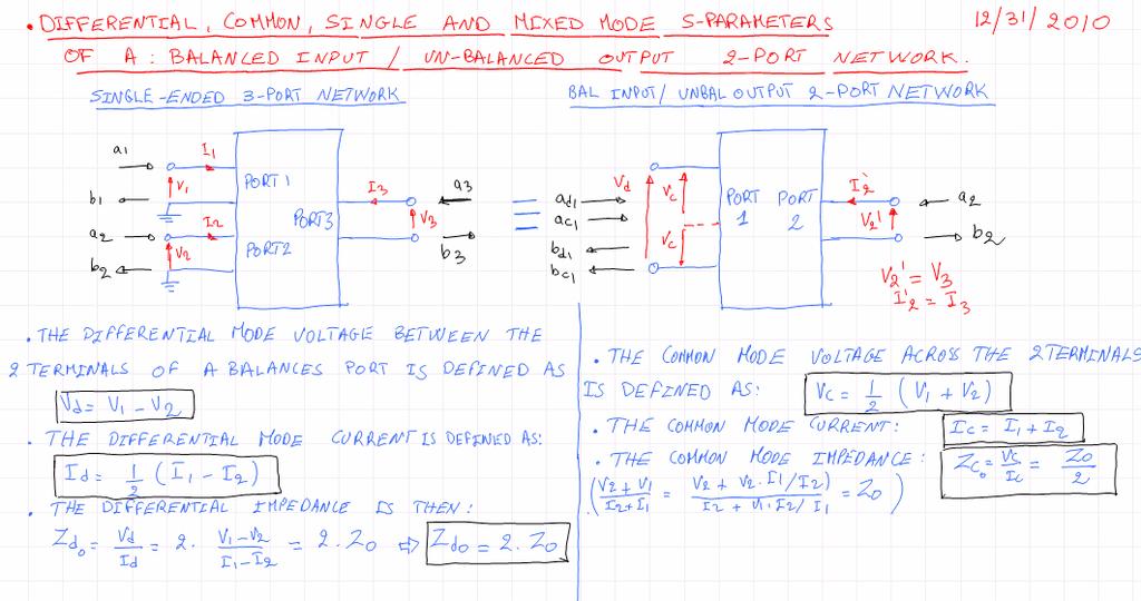
3 3 Fig6. Single ended reverse gain of the amplifier pair. The measured single ended s-parameters need to be converted to differential, common and mixed mode s-parameters to describe the behavior of the LNA to different mode signals. Fig7. Shows the needed s-parameters for this network. Fig8.Circuit used to compute Sdd11 in MWO. STIMULUS LOGICAL PORT 1 LOGICAL PORT 2 R E S P O N S E LOGICAL PORT 1 LOGICAL PORT 2 DIFF MODE COM MODE DIFF MODE COM MODE SE Sdd11 Sdc11 Sds12 Scd11 Scc11 Scs12 SE Ssd21 Ssc21 Sss22 Fig7. Mixed mode s-parameters for a 2 port network where: Port1 is balanced and port 2 is single ended. The network is fully characterized by these 9 parameters. Fig9. Sdd11 relative to 100 Ohm computed from measured single ended s-parameters. Fig9 is the input return loss of the LNA relative to 100 Ohm impedance. Fig10. Is the return loss relative to 200 Ohm impedance. The different sparameters are computed in Microwave office (MWO) [4] design environment using the MMCONV mixed mode converter function built into MWO. Fig8 shows the circuit used to compute the differential mode input reflection coefficient Sdd11 and the actual result (Fig9). Fig10. Sdd11 relative to 200 Ohm impedance.
 showing reflective rejection of common mode signals at the input of the LNA. Fig12.")
4 4 Fig14. Commom mode to differential conversion parameter showing low conversion factor. Fig11. Complex Sdd11 of the LNA on a Smith Chart. The markers display de-normalized impedance. Fig15. Common mode input reflection coefficient (relative to 25 Ohm) showing reflective rejection of common mode signals at the input of the LNA. Fig12. Real and Imaginary parts of the input differential impedance Fig16. Differential to commom mode conversion parameter showing low conversion factor.(low EMI generation) Fig13. Return loss of the LNA output showing good impedance match to 50 Ohm.
5 5 Fig17. Differential mode Gain Ssd21 Fig20. Reverse common mode Gain showing good isolation. Fig18. Ssc21 common mode noise at balanced port1 transferred to single ended port2 Fig21. Common Mode Rejection Ratio (CMRR) shown with the Differential and Common mode Gains. The Common mode rejection ratio is the ratio of the differential to common mode gains of the amplifier [5]: CMRR [db] =20 x log10( Ssd21 / Scd21 ) or: CMRR[dB] = Ssd21[dB] Scd21[dB] The CMRR varies between 24dB and 15.2dB on the MHz band. Fig19. Reverse Differential Gain showing good isolation. IV. S-PARAMETERS MEASUREMENTS ON A WIDE BANDWIDTH To check the stability of the amplifier outside its operating band, an sparameter measurement was made using the ZVA24 VNA. The measurement settings: 10MHz 24GHz Port Power: -40dBm SOLT CAL 3 ports calibrated: Port1, Port3 and Port2 AVG: 100 averages. Low signal power was used to keep the LNA operating on its linear range. The signal to noise ratio at the VNA receivers is low that is why 100 sweeps were averaged, this will reduce trace noise.
6 6 Fig. The magnitude of the input reflection coefficient of the MWA LNA REV B measured to 24GHz. Sdd11[dB] is < 0 up to 24 GHz. Fig. reverse gain of the LNA showing good output to input isolation. Fig. The magnitude of the output reflection coefficient of the MWA LNA. Sss22[dB] is < 0 up to 24 GHz, the positive Sss22 at about 20GHz is due to a lot of trace noise probably caused by low signal strength reaching the measurement receiver of the VNA. Similar trace noise levels are seen on Sdd11 curve. Fig. Common mode gain of the amplifier shows high CM gain out of the MWA band. The CM gain peaks at 1.2GHz. The relatively high common mode gain should not be a problem since the antenna has high common mode reflection coefficient (Scc11) which means mos of the common mode signals will be reflected at te antenna ports. The Rolett s stability factor (K-factor) was computed from the measured s-parameters. The necessary and sufficient conditional for unconditional stability ( stability at all possible input and output impedances): K > 1 and B1 >0 : th determinant of the s-matrix and B1 is the auxilary stability factor. Fig. differential Gain of the LNA.

7 7 The input and output stability circles are shown below but all the instability circles are outside the smith chart since the LNA is unconditionally stable. Fig. Circuit used to compute the differential mode stability factor. Fig. input stability circles. Fig. K-factor of the MWA LNA showing unconditional stability up to 24GHz since K< 1. Fig. Output stability circles. Fig. Auxilary stability facor B1: B1 >0.
8 8 Fig. Circuit used to compute the common mode stability factor. Fig. Auxilary staility factor B1 >0 Fig. Common mode Stability factor on a widebandwidth. K > 1 V. EFFECT OF THE ANTENNA IMPEDANCE ON THE LNA The measured LNA sparameters were used together with the measured antenna impedance to compute the transducer power gain of the amplifier. The Ssd21 parameter shown on Fig 17 is the power gain of the amplifier when its input (balanced input) is terminated with 100 Ohm impedance and when its output (unbalanced) is terminated with a 50 ohm impedance. The input of LNA is connected to the dipole antenna through wire terminals or twin leads. The impedance of the antenna was measured before and data reported on the MWA antenna impedance Memo. The figure below shows the differential gain of the amplifier when its input is terminated with 100 ohm and when it is terminated with the antenna impedance. Fig. common mode stability factor on the MWA Band. Fig. Differential gain of the amplifier when its input (balanced) is terminated with: 100 Ohm impedance( red curve) and the antenna impedance(lack curve) VI. NOISE MEASUREMENTS The noise of the MWA LNA was measured using a 3dB 180deg coupler or balun that transforms the balanced input of the LNA to unbalanced port where a calibrated HP346C noise source was connected. The noise output of the noise generator


9 9 was too high and its output impedance changes between ON/OFF states. A 10dB pad was inserted between the noise source and the balun to improve the match. Since the LNA was a bare printed circuit board with no metal enclosure, an RFI tight enclosure was used to do the measurement to avoid RFI pick up which can saturate the amplifier and add noise to the data. A bias tee was connected to the output of the amplifier to inject bias. The setup schematics are shown on Fig22. It was found out that the bias tee allows the FM band signals to leak into the amplifier. This was caused by a low bypass capacitance on the DC port of the bias tee, a capacitor was mounted on the bias tee to cut the FM band signals. Fig24. shows an inside view of the modified bias tee. Fig22. setup used to do noise measurement. A picture of the actual setup is shown on Fig23: Fig24. Mini circuits bias tee with an additional capacitor on the Dc port. The loss of the Balun, 10dB attenuator and cabling was measured using a 3 port VNA and was used to correct the measured noise. Fig25 shows a plot of the noise source ENR (excess noise ratio) and a the Y-factor: HP 346C 14dB ENR Calibrated 10dB Pad MWA LNA REV B To improve the output With SMA connectors Match of the Noise At the input Source Mini circuits balun Bias Tee To Bias the LNA Preamp to improve The SNR at the input Of the spectrum analyzer $20 RFI Shielded box from Fry s! Fig23. Noise measurement setup. Fig25. Top: ENR of the noise source: there is only one calibration frequency point on the band, the ENR table was interpolated to do the measurement since it is assumed the signal output is flat. Bottom: the Yfactor = Phot/Pcold when the noise source was turned ON/OFF. The Yfactor on this figure was corrected for the noise of a post amplifier used
10 10 between the LNA under test and the spectrum analyzer to improve the signal to noise ratio at the input of the spectrum analyzer The measured noise of the LNA including the cables, 10dB pad and balun is shown on Fig26. [2] ure_simulator/evaluating_balanced_devices_balance_unbalance_conversi on.htm [3] &cc=US&lc=eng [4] [5] "Microwave Differential Circuit Design Using Mixed Mode S-Parameters" William R. Eisenstadt, Bob Stengel, Bruce M. Thompson Appendix, Artech House Publishers (May 1, 2006), ISBN-10: Fig26. Uncorrected noise temperature of the LNA: this noise includes the losses of the cables and the balun. The measured loss of cables, pad and balun was used to get the noise of the LNA by itself. Fig27. Plot showing the corrected noise of the LNA VII. CONCLUSION & DISCUSSION VIII. ACCOMPANYING FILES AKNOLWEDGEMENT REFERENCES [1] tors/fet/atf-54143/
11
12
13
14
15
MWA Antenna Impedance Measurements
 1 MWA Antenna Impedance Measurements Hamdi Mani, Judd Bowman Abstract we describe measurements of the differential output impedance of the MWA bowtie antenna. The data shows that the magnitude of the impedance
This article describes the design of a multiband,
 A Low-Noise Amplifier for 2 GHz Applications Using the NE334S01 Transistor By Ulrich Delpy NEC Electronics (Europe) This article describes the design of a multiband, low-noise amplifier (LNA) using the
Circuit Characterization with the Agilent 8714 VNA
 Circuit Characterization with the Agilent 8714 VNA By: Larry Dunleavy Wireless and Microwave Instruments University of South Florida Objectives 1) To examine the concepts of reflection, phase shift, attenuation,
Application Note 5525
 Using the Wafer Scale Packaged Detector in 2 to 6 GHz Applications Application Note 5525 Introduction The is a broadband directional coupler with integrated temperature compensated detector designed for
NATIONAL UNIVERSITY of SINGAPORE
 NATIONAL UNIVERSITY of SINGAPORE Faculty of Engineering Electrical & Computer Engineering Department EE3104 Introduction to RF and Microwave Systems & Circuits Experiment 1 Familiarization on VNA Calibration
Maxim > Design Support > Technical Documents > Application Notes > Wireless and RF > APP 3571
 Maxim > Design Support > Technical Documents > Application Notes > Wireless and RF > APP 3571 Keywords: automotive keyless entry, MAX2640, LNA, 315MHz, RKE, stability, automotive, keyless entry APPLICATION
A True Differential Millimeter Wave System with Port Power Control. Presented by: Suren Singh
 A True Differential Millimeter Wave System with Port Power Control Presented by: Suren Singh Agenda Need for True Differential and RF Power Control Vector Network Analyzer RF Port Power Control Port Power
Platform Migration 8510 to PNA. Graham Payne Application Engineer Agilent Technologies
 Platform Migration 8510 to PNA Graham Payne Application Engineer Agilent Technologies We set the standard... 8410 8510 When we introduced the 8510, we changed the way S-parameter measurements were made!
Advanced Test Equipment Rentals ATEC (2832)
") Established 1981 Advanced Test Equipment Rentals www.atecorp.com 800-404-ATEC (2832) Agilent 2-Port and 4-Port PNA-X Network Analyzer N5249A - 10 MHz to 8.5 GHz N5241A - 10 MHz to 13.5 GHz N5242A - 10
Established 1981 Advanced Test Equipment Rentals www.atecorp.com 800-404-ATEC (2832) Agilent 2-Port and 4-Port PNA-X Network Analyzer N5249A - 10 MHz to 8.5 GHz N5241A - 10 MHz to 13.5 GHz N5242A - 10
Range Considerations for RF Networks
 TI Technology Days 2010 Range Considerations for RF Networks Richard Wallace Abstract The antenna can be one of the most daunting components of wireless designs. Most information available relates to large
Keysight 2-Port and 4-Port PNA-X Network Analyzer
 Keysight 2-Port and 4-Port PNA-X Network Analyzer N5249A - 0 MHz to 8.5 GHz N524A - 0 MHz to 3.5 GHz N5242A - 0 MHz to 26.5 GHz Data Sheet and Technical Specifications Documentation Warranty THE MATERIAL
New Ultra-Fast Noise Parameter System... Opening A New Realm of Possibilities in Noise Characterization
 New Ultra-Fast Noise Parameter System... Opening A New Realm of Possibilities in Noise Characterization David Ballo Application Development Engineer Agilent Technologies Gary Simpson Chief Technology Officer
Configuration of PNA-X, NVNA and X parameters
 Configuration of PNA-X, NVNA and X parameters VNA 1. S-Parameter Measurements 2. Harmonic Measurements NVNA 3. X-Parameter Measurements Introducing the PNA-X 50 GHz 43.5 GHz 26.5 GHz 13.5 GHz PNA-X Agilent
RF Characterization Report
 SMA-J-P-H-ST-MT1 Mated with: RF316-01SP1-01BJ1-0305 Description: 50-Ω SMA Board Mount Jack, Mixed Technology Samtec, Inc. 2005 All Rights Reserved Table of Contents Introduction...1 Product Description...1
Wide-Band Two-Stage GaAs LNA for Radio Astronomy
 Progress In Electromagnetics Research C, Vol. 56, 119 124, 215 Wide-Band Two-Stage GaAs LNA for Radio Astronomy Jim Kulyk 1,GeWu 2, Leonid Belostotski 2, *, and James W. Haslett 2 Abstract This paper presents
Spurious and Stability Analysis under Large-Signal Conditions using your Vector Network Analyser
 Spurious and Stability Analysis under Large-Signal Conditions using your Vector Network Analyser An application of ICE June 2012 Outline Why combining Large-Signal and Small-Signal Measurements Block Diagram
Bias-T Design Considerations for the LWA Brian Hicks and Bill Erickson May 21, 2008
 Bias-T Design Considerations for the LWA Brian Hicks and Bill Erickson May 21, 2008 The strawman design document [1] for the LWA suggests that the Front End Electronics (FEE) could be powered through the
High Intercept Low Noise Amplifier for 1.9 GHz PCS and 2.1 GHz W-CDMA Applications using the ATF Enhancement Mode PHEMT
 High Intercept Low Noise Amplifier for 1.9 GHz PCS and 2.1 GHz W-CDMA Applications using the ATF-55143 Enhancement Mode PHEMT Application Note 1241 Introduction Avago Technologies ATF-55143 is a low noise
Features and Technical Specifications
 Features and Technical Specifications PRODU C T SUM M AR Y The HL9402 is a signal splitter and combiner that offers industry-best amplitude and phase match over a bandwidth of 500 khz to 20 GHz (-3 db).
Application Note 1299
 A Low Noise High Intercept Point Amplifier for 9 MHz Applications using ATF-54143 PHEMT Application Note 1299 1. Introduction The Avago Technologies ATF-54143 is a low noise enhancement mode PHEMT designed
Demo Circuit DC550A Quick Start Guide.
 May 12, 2004 Demo Circuit DC550A. Introduction Demo circuit DC550A demonstrates operation of the LT5514 IC, a DC-850MHz bandwidth open loop transconductance amplifier with high impedance open collector
Application Note No. 168
 Application Note, Rev. 1.2, November 2008 Application Note No. 168 BFP740F SiGe:C Ultra Low Noise RF Transistor in 5 6 LNA Application with 16 db Gain, 1.3 db Noise Figure & 1 microsecond Turn-On / Turn-Off
Agilent 2-Port and 4-Port PNA-X Network Analyzer. N5241A - 10 MHz to 13.5 GHz N5242A - 10 MHz to 26.5 GHz Data Sheet and Technical Specifications
 Agilent 2-Port and 4-Port PNA-X Network Analyzer N5241A - 10 MHz to 13.5 GHz N5242A - 10 MHz to 26.5 GHz Data Sheet and Technical Specifications Documentation Warranty THE MATERIAL CONTAINED IN THIS DOCUMENT
EXPERIMENT EM3 INTRODUCTION TO THE NETWORK ANALYZER
 ECE 351 ELECTROMAGNETICS EXPERIMENT EM3 INTRODUCTION TO THE NETWORK ANALYZER OBJECTIVE: The objective to this experiment is to introduce the student to some of the capabilities of a vector network analyzer.
EE290C - Spring 2004 Advanced Topics in Circuit Design
 EE290C - Spring 2004 Advanced Topics in Circuit Design Lecture #3 Measurements with VNA and TDR Ben Chia Tu-Th 4 5:30pm 531 Cory Agenda Relationships between time domain and frequency domain TDR Time Domain
Network Analysis Seminar. Cables measurement
 Network Analysis Seminar Cables measurement Agenda 1. Device Under Test: Cables & Connectors 2. Instrument for cables testing: Network Analyzer 3. Measurement: Frequency Domain 4. Measurement: Time Domain
TEST EQUIPMENT PLUS. Signal Hound USB-SA44B / USB-TG44A. Application Note 1: The Smith Chart. Rev. 0
 Rev. 0 TEST EQUIPMENT PLUS Signal Hound USB-SA44B / USB-TG44A Application Note 1: The Smith Chart USING THE SMITH CHART Chapter 1 1 Using the Smith Chart Making Single-Frequency Vector Impedance Measurements
Top View (Near-side) Side View Bottom View (Far-side) .89±.08. 4x.280. Orientation Marker Orientation Marker.
 Side View Bottom View (Far-side) .89±.08. 4x.280. Orientation Marker Orientation Marker.") Model B2F2AHF Ultra Low Profile 168 Balun Ω to 2Ω Balanced Description The B2F2AHF is a low profile sub-miniature balanced to unbalanced transformer designed for differential input locations on data conversion
Model B2F2AHF Ultra Low Profile 168 Balun Ω to 2Ω Balanced Description The B2F2AHF is a low profile sub-miniature balanced to unbalanced transformer designed for differential input locations on data conversion
Opamp stability using non-invasive methods
 Opamp stability using non-invasive methods Opamps are frequently use in instrumentation systems as unity gain analog buffers, voltage reference buffers and ADC input buffers as well as low gain preamplifiers.
Model BD1631J50100AHF
 Model BD1631J51AHF Ultra Low Profile 85 Balun 5Ω to 1Ω Balanced Description The BD1631J51AHF is a low profile sub-miniature balanced to unbalanced transformer designed for differential inputs and output
Product Note 75 DLPS, a Differential Load Pull System
 63 St-Regis D.D.O, Quebec H9B 3H7, Canada Tel 54-684-4554 Fax 54-684-858 E-mail: info@ focus-microwaves.com Website: http://www.focus-microwaves.com Product Note 75 DLPS, a Differential Load Pull System
You will need the following pieces of equipment to complete this experiment: Wilkinson power divider (3-port board with oval-shaped trace on it)
") UNIVERSITY OF TORONTO FACULTY OF APPLIED SCIENCE AND ENGINEERING The Edward S. Rogers Sr. Department of Electrical and Computer Engineering ECE422H1S: RADIO AND MICROWAVE WIRELESS SYSTEMS EXPERIMENT 1:
UNIVERSITY OF TORONTO FACULTY OF APPLIED SCIENCE AND ENGINEERING The Edward S. Rogers Sr. Department of Electrical and Computer Engineering ECE422H1S: RADIO AND MICROWAVE WIRELESS SYSTEMS EXPERIMENT 1:
ECEN 5014, Spring 2009 Special Topics: Active Microwave Circuits Zoya Popovic, University of Colorado, Boulder
 ECEN 5014, Spring 2009 Special Topics: Active Microwave Circuits Zoya opovic, University of Colorado, Boulder LECTURE 3 MICROWAVE AMLIFIERS: INTRODUCTION L3.1. TRANSISTORS AS BILATERAL MULTIORTS Transistor
1 of 7 12/20/ :04 PM
 1 of 7 12/20/2007 11:04 PM Trusted Resource for the Working RF Engineer [ C o m p o n e n t s ] Build An E-pHEMT Low-Noise Amplifier Although often associated with power amplifiers, E-pHEMT devices are
ECE 145A/218A, Lab Project #1b: Transistor Measurement.
 ECE 145A/218A, Lab Project #1b: Transistor Measurement. September 28, 2017 OVERVIEW... 2 GOALS:... 2 SAFETY PRECAUTIONS:... 2 READING:... 2 TRANSISTOR RF CHARACTERIZATION.... 3 DC BIAS CIRCUITS... 3 TEST
UM User manual for the BGU7004 GPS LNA evaluation board. Document information. Keywords LNA, GPS, BGU7004. Abstract
 User manual for the BGU7004 GPS LNA evaluation board Rev. 1.0 14 June 2011 User manual Document information Info Keywords Abstract Content LNA, GPS, BGU7004 This document explains the BGU7004 AEC-Q100
Challenges and Solutions for Removing Fixture Effects in Multi-port Measurements
 DesignCon 2008 Challenges and Solutions for Removing Fixture Effects in Multi-port Measurements Robert Schaefer, Agilent Technologies schaefer-public@agilent.com Abstract As data rates continue to rise
Application Note 5057
 A 1 MHz to MHz Low Noise Feedback Amplifier using ATF-4143 Application Note 7 Introduction In the last few years the leading technology in the area of low noise amplifier design has been gallium arsenide
Impedance 50 (75 connectors via adapters)
") VECTOR NETWORK ANALYZER PLANAR 304/1 DATA SHEET Frequency range: 300 khz to 3.2 GHz Measured parameters: S11, S21, S12, S22 Dynamic range of transmission measurement magnitude: 135 db Measurement time
VECTOR NETWORK ANALYZER PLANAR 304/1 DATA SHEET Frequency range: 300 khz to 3.2 GHz Measured parameters: S11, S21, S12, S22 Dynamic range of transmission measurement magnitude: 135 db Measurement time
UNIVERSITI MALAYSIA PERLIS
 UNIVERSITI MALAYSIA PERLIS SCHOOL OF COMPUTER & COMMUNICATIONS ENGINEERING EKT 341 LABORATORY MODULE LAB 2 Antenna Characteristic 1 Measurement of Radiation Pattern, Gain, VSWR, input impedance and reflection
MICROWAVE MICROWAVE TRAINING BENCH COMPONENT SPECIFICATIONS:
 Microwave section consists of Basic Microwave Training Bench, Advance Microwave Training Bench and Microwave Communication Training System. Microwave Training System is used to study all the concepts of
Gain Lab. Image interference during downconversion. Images in Downconversion. Course ECE 684: Microwave Metrology. Lecture Gain and TRL labs
 Gain Lab Department of Electrical and Computer Engineering University of Massachusetts, Amherst Course ECE 684: Microwave Metrology Lecture Gain and TRL labs In lab we will be constructing a downconverter.
Vector Network Analyzer Application note
 Vector Network Analyzer Application note Version 1.0 Vector Network Analyzer Introduction A vector network analyzer is used to measure the performance of circuits or networks such as amplifiers, filters,
Hot S 22 and Hot K-factor Measurements
 Application Note Hot S 22 and Hot K-factor Measurements Scorpion db S Parameter Smith Chart.5 2 1 Normal S 22.2 Normal S 22 5 0 Hot S 22 Hot S 22 -.2-5 875 MHz 975 MHz -.5-2 To Receiver -.1 DUT Main Drive
Fast network analyzers also for balanced measurements
 GENERAL PURPOSE Network analyzers 44297/5 FIG 1 The new Vector Network Analyzer R&S ZVB, here with four-port configuration. Vector Network Analyzers R&S ZVB Fast network analyzers also for balanced measurements
Radio ETI031 Laboratory Experiments 2: VECTOR NETWORK ANALYSER, ANTENNA and RECEIVER MEASUREMENTS
 Lund University Electrical and Information Technology GJ 2007-09-30 Radio ETI031 Laboratory Experiments 2: VECTOR NETWORK ANALYSER, ANTENNA and RECEIVER MEASUREMENTS Göran Jönsson 2007 Objectives: Part
Characterization of SPDT RF Switch (Mini-circuits MSP2TA )
") Characterization of SPDT RF Switch (Mini-circuits ) Raul Monsalve SESE, Arizona State University August 18, 2014 2 Description The RF switch Mini-circuits was characterized in terms of repeatability and
Characterization of SPDT RF Switch (Mini-circuits ) Raul Monsalve SESE, Arizona State University August 18, 2014 2 Description The RF switch Mini-circuits was characterized in terms of repeatability and
Keysight Technologies Network Analyzer Measurements: Filter and Amplifier Examples. Application Note
 Keysight Technologies Network Analyzer Measurements: Filter and Amplifier Examples Application Note Introduction Both the magnitude and phase behavior of a component are critical to the performance of
Agilent Accurate Measurement of Packaged RF Devices. White Paper
 Agilent Accurate Measurement of Packaged RF Devices White Paper Slide #1 Slide #2 Accurate Measurement of Packaged RF Devices How to Measure These Devices RF and MW Device Test Seminar 1995 smafilt.tif
Development of a noval Switched Beam Antenna for Communications
 Master Thesis Presentation Development of a noval Switched Beam Antenna for Communications By Ashraf Abuelhaija Supervised by Prof. Dr.-Ing. Klaus Solbach Institute of Microwave and RF Technology Department
High Speed Characterization Report
 SSW-1XX-22-X-D-VS Mates with TSM-1XX-1-X-DV-X Description: Surface Mount Terminal Strip,.1 [2.54mm] Pitch, 13.59mm (.535 ) Stack Height Samtec, Inc. 25 All Rights Reserved Table of Contents Connector Overview...
Parameter Symbol Units MIN MAX. RF Input power (CW) Pin dbm +37
 Pin dbm +37") AMT-A0246 4 GHz to 8 GHz Broadband LNA with 5 W Protection Limiter Data Sheet Features 4 GHz to 8 GHz Frequency Range +37 dbm (5W) CW Pin survival Gain 28 db Typical Gain Flatness ± 0.6 db Typical 2.2
AMT-A0246 4 GHz to 8 GHz Broadband LNA with 5 W Protection Limiter Data Sheet Features 4 GHz to 8 GHz Frequency Range +37 dbm (5W) CW Pin survival Gain 28 db Typical Gain Flatness ± 0.6 db Typical 2.2
Parameter Symbol Units MIN MAX. RF Input power (CW) Pin dbm +20
 Pin dbm +20") AMT-A0011 100MHz to 2000MHz Ultra Flat Gain with High Linearity Amplifier Data Sheet Features Ultra Flat Gain < ± 0.15 db from 300 to 1400MHz Frequency Range Gain 15 db, BP filter provides for zero gain
AMT-A0011 100MHz to 2000MHz Ultra Flat Gain with High Linearity Amplifier Data Sheet Features Ultra Flat Gain < ± 0.15 db from 300 to 1400MHz Frequency Range Gain 15 db, BP filter provides for zero gain
FieldFox Handheld Education Series Part 3: Calibration Techniques for Precise Field Measurements
 FieldFox Handheld Education Series Part 3: Calibration Techniques for Precise Field Measurements FieldFox Handheld Education Series Interference Testing Cable and Antenna Measurements Calibration Techniques
PA FAN PLATE ASSEMBLY 188D6127G1 SYMBOL PART NO. DESCRIPTION. 4 SBS /10 Spring nut. 5 19A702339P510 Screw, thread forming, flat head.
 MAINTENANCE MANUAL 851-870 MHz, 110 WATT POWER AMPLIFIER 19D902797G5 TABLE OF CONTENTS Page DESCRIPTION.............................................. Front Page SPECIFICATIONS.................................................
Top View (Near-side) Side View Bottom View (Far-side) ± ±.08. 4x.28. Orientation Marker Balanced port 1.
 Side View Bottom View (Far-side) ± ±.08. 4x.28. Orientation Marker Balanced port 1.") Model BD2FAHF Ultra Low Profile 168 Balun Ω to Ω Balanced Description The BD2FAHF is a low profile sub-miniature balanced to unbalanced transformer designed for differential input locations on data conversion
Model BD2FAHF Ultra Low Profile 168 Balun Ω to Ω Balanced Description The BD2FAHF is a low profile sub-miniature balanced to unbalanced transformer designed for differential input locations on data conversion
Network Analysis Basics
 Adolfo Del Solar Application Engineer adolfo_del-solar@agilent.com MD1010 Network B2B Agenda Overview What Measurements do we make? Network Analyzer Hardware Error Models and Calibration Example Measurements
There is a twenty db improvement in the reflection measurements when the port match errors are removed.
 ABSTRACT Many improvements have occurred in microwave error correction techniques the past few years. The various error sources which degrade calibration accuracy is better understood. Standards have been
ELEC 0017: ELECTROMAGNETIC COMPATIBILITY LABORATORY SESSIONS
 Academic Year 2015-2016 ELEC 0017: ELECTROMAGNETIC COMPATIBILITY LABORATORY SESSIONS V. BEAUVOIS P. BEERTEN C. GEUZAINE 1 CONTENTS: EMC laboratory session 1: EMC tests of a commercial Christmas LED light
The Design of A 125W L-Band GaN Power Amplifier
 Sheet Code RFi0613 White Paper The Design of A 125W L-Band GaN Power Amplifier This paper describes the design and evaluation of a single stage 125W L-Band GaN Power Amplifier using a low-cost packaged
Design of Low Noise Amplifier Using Feedback and Balanced Technique for WLAN Application
 Available online at www.sciencedirect.com Procedia Engineering 53 ( 2013 ) 323 331 Malaysian Technical Universities Conference on Engineering & Technology 2012, MUCET 2012 Part 1- Electronic and Electrical
High Speed Characterization Report
 QTH-030-01-L-D-A Mates with QSH-030-01-L-D-A Description: High Speed Ground Plane Header Board-to-Board, 0.5mm (.0197 ) Pitch, 5mm (.1969 ) Stack Height Samtec, Inc. 2005 All Rights Reserved Table of Contents
Millimeter Signal Measurements: Techniques, Solutions and Best Practices
 New Network Analyzer platform Millimeter Signal Measurements: Techniques, Solutions and Best Practices Phase Noise measurements update 1 N522XA PNA Series Network Analyzer Introducing Highest Performance
Vector Network Analyzers T - Series
 Datasheet Vector Network Analyzers T - Series Wide dynamic range 130 db typ. Low noise level < -120 dbm Low trace noise 1 mdb rms High measurement speed 125ms/point High effective directivity > 45 db Remote
ATF High Intercept Low Noise Amplifier for the MHz PCS Band using the Enhancement Mode PHEMT
 ATF-54143 High Intercept Low Noise Amplifier for the 185 191 MHz PCS Band using the Enhancement Mode PHEMT Application Note 1222 Introduction Avago Technologies ATF-54143 is a low noise enhancement mode
Application Note 5379
 VMMK-1225 Applications Information Application Note 5379 Introduction The Avago Technologies VMMK-1225 is a low noise enhancement mode PHEMT designed for use in low cost commercial applications in the
Compact Series: S5065 & S5085 Vector Network Analyzers KEY FEATURES
 Compact Series: S5065 & S5085 Vector Network Analyzers KEY FEATURES Frequency range: 9 khz - 6.5 or 8.5 GHz Measured parameters: S11, S12, S21, S22 Wide output power adjustment range: -50 dbm to +5 dbm
Frequency and Time Domain Representation of Sinusoidal Signals
 Frequency and Time Domain Representation of Sinusoidal Signals By: Larry Dunleavy Wireless and Microwave Instruments University of South Florida Objectives 1. To review representations of sinusoidal signals
Model B0922N7575AHF Rev B. Ultra Low Profile 0404 Balun
 Model B9N7575AHF Ultra Low Profile 44 Balun 75Ω to 75Ω Balanced Description The B9N7575AHF is a low profile, low impedance mm square subminiature wideband unbalanced to balanced transformer designed for
EMC Near-field Probes + Wideband Amplifier
 1 Introduction The H20, H10, H5 and E5 are magnetic field (H) and electric field (E) probes for radiated emissions EMC precompliance measurements. The probes are used in the near field of sources of electromagnetic
Designing a 960 MHz CMOS LNA and Mixer using ADS. EE 5390 RFIC Design Michelle Montoya Alfredo Perez. April 15, 2004
 Designing a 960 MHz CMOS LNA and Mixer using ADS EE 5390 RFIC Design Michelle Montoya Alfredo Perez April 15, 2004 The University of Texas at El Paso Dr Tim S. Yao ABSTRACT Two circuits satisfying the
1000BASE-T1 EMC Test Specification for Common Mode Chokes
 IEEE 1000BASE-T1 EMC Test Specification for Common Mode Chokes Version 1.0 Author & Company Dr. Bernd Körber, FTZ Zwickau Title 1000BASE-T1 EMC Test Specification for Common Mode Chokes Version 1.0 Date
ME1000 RF Circuit Design. Lab 4. Filter Characterization using Vector Network Analyzer (VNA)
") ME1000 RF Circuit Design Lab 4 Filter Characterization using Vector Network Analyzer (VNA) This courseware product contains scholarly and technical information and is protected by copyright laws and international
ME1000 RF Circuit Design Lab 4 Filter Characterization using Vector Network Analyzer (VNA) This courseware product contains scholarly and technical information and is protected by copyright laws and international
87415A microwave system amplifier A microwave. system amplifier A microwave system amplifier A microwave.
 20 Amplifiers 83020A microwave 875A microwave 8308A microwave 8307A microwave 83006A microwave 8705C preamplifier 8705B preamplifier 83050/5A microwave The Agilent 83006/07/08/020/050/05A test s offer
MASSACHUSETTS INSTITUTE OF TECHNOLOGY HAYSTACK OBSERVATORY WESTFORD, MASSACHUSETTS
 To: From: EDGES MEMO #075 MASSACHUSETTS INSTITUTE OF TECHNOLOGY HAYSTACK OBSERVATORY WESTFORD, MASSACHUSETTS 01886 July 27, 2011 Telephone: 781-981-5407 Fax: 781-981-0590 EDGES Group Alan E.E. Rogers and
Vector Network Analyzers (VERY) Basics. Tom Powers USPAS SRF Testing Course 19 Jan. 2014
 Basics. Tom Powers USPAS SRF Testing Course 19 Jan. 2014") Vector Network Analyzers (VERY) Basics Tom Powers USPAS SRF Testing Course 19 Jan. 2014 S-Parameters A scattering matrix relates the voltage waves incident on the ports of a network to those reflected
Vector Network Analyzers (VERY) Basics Tom Powers USPAS SRF Testing Course 19 Jan. 2014 S-Parameters A scattering matrix relates the voltage waves incident on the ports of a network to those reflected
Features and Technical Specifications
 Features and Technical Specifications PRODU C T SUM M AR Y The HL9404 is a signal splitter and combiner that offers industry-best amplitude and phase match over a bandwidth of 500 khz to 40 GHz (-3 db).
Model BD4859L50100A00 Rev A
 Model BD4859L51A Ultra Small Low Profile 63 Balun 5Ω to 1Ω Balanced Description The BD4859L51A is an ultra-small low profile balanced to unbalanced transformer designed for differential inputs and output
Department of Electrical and Computer Engineering ECE332. Lab 3: High Frequency Measurements
 Department of Electrical and Computer Engineering ECE332 Version: 1.3.1 Revised: April 30, 2011 Contents 1 Pre-Lab Assignment 2 2 Introduction 2 2.1 Vector Network Analyzer.............................
Bill Ham Martin Ogbuokiri. This clause specifies the electrical performance requirements for shielded and unshielded cables.
 098-219r2 Prepared by: Ed Armstrong Zane Daggett Bill Ham Martin Ogbuokiri Date: 07-24-98 Revised: 09-29-98 Revised again: 10-14-98 Revised again: 12-2-98 Revised again: 01-18-99 1. REQUIREMENTS FOR SPI-3
Application Note No. 149
 Application Note, Rev. 1.2, February 2008 1.8 V, 2.6 ma Low Noise Amplifier for 1575 MHz GPS L1 Frequency with the BFP405 RF Transistor Small Signal Discretes Edition 2008-02-22 Published by Infineon Technologies
Application Note No. 116
 Application Note, Rev. 1.2, August 2007 Application Note No. 116 BFR740L3 Ultra Low Noise SiGe:C RF Transistor as 2110-2170 MHz UMTS Low Noise Amplifier RF & Protection Devices Edition 2007-08-30 Published
Model BD1722J50100A00
 Ultra Low Profile 85 Balun 5Ω to 1Ω Balanced Description The BD1722J51A is a low profile sub-miniature balanced to unbalanced transformer designed for differential inputs and output locations on next generation
Migrating 4195A to E5061B LF-RF Network Analyzer. April 2010 Agilent Technologies
 Migrating 4195A to E61B LF-RF Network Analyzer April 2010 Agilent Technologies Page 1 Contents Overview of 4195A to E61B migration Migrating 4195A to E61B in network measurements Migrating 4195A to E61B
Figure 1 Photo of an Upgraded Low Band Receiver
 NATIONAL RADIO ASTRONOMY OBSERVATORY SOCORRO, NEW MEXICO EVLA TECHNICAL REPORT #175 LOW BAND RECEIVER PERFORMANCE SEPTMBER 27, 2013 S.DURAND, P.HARDEN Upgraded low band receivers, figure 1, were installed
CHAPTER 4. Practical Design
 CHAPTER 4 Practical Design The results in Chapter 3 indicate that the 2-D CCS TL can be used to synthesize a wider range of characteristic impedance, flatten propagation characteristics, and place passive
Model BD3238N5050AHF. Ultra Low Profile 0404 Balun
 Model BD338N55AHF Ultra Low Profile 44 Balun 5Ω to 5Ω Balanced Description The BD338N55AHF is a low cost, low profile sub-miniature unbalanced to balanced transformer designed for differential inputs and
Parameter Symbol Units MIN MAX. RF Input power (CW) Pin dbm +20. DC Current A 1.6
 Pin dbm +20. DC Current A 1.6") AMT-A0030 2 GHz to 18 GHz 8W 41 db Gain Broadband High Power Amplifier Module Data Sheet Features 2 GHz to 18 GHz Frequency Range Typical Psat power > +39 dbm Gain 41 db High Efficiency Internally Regulated
AMT-A0030 2 GHz to 18 GHz 8W 41 db Gain Broadband High Power Amplifier Module Data Sheet Features 2 GHz to 18 GHz Frequency Range Typical Psat power > +39 dbm Gain 41 db High Efficiency Internally Regulated
Keysight 2-Port and 4-Port PNA-X Network Analyzer
 Keysight 2-Port and 4-Port PNA-X Network Analyzer N5249A - 0 MHz to 8.5 GHz N524A - 0 MHz to 3.5 GHz N5242A - 0 MHz to 26.5 GHz Data Sheet and Technical Specifications Documentation Warranty THE MATERIAL
S.A. Torchinsky, A. van Ardenne, T. van den Brink-Havinga, A.J.J. van Es, A.J. Faulkner (eds.) 4-6 November 2009, Château de Limelette, Belgium
 4-6 November 2009, Château de Limelette, Belgium") WIDEFIELD SCIENCE AND TECHNOLOGY FOR THE SKA SKADS CONFERENCE 2009 S.A. Torchinsky, A. van Ardenne, T. van den Brink-Havinga, A.J.J. van Es, A.J. Faulkner (eds.) 4-6 November 2009, Château de Limelette,
WIDEFIELD SCIENCE AND TECHNOLOGY FOR THE SKA SKADS CONFERENCE 2009 S.A. Torchinsky, A. van Ardenne, T. van den Brink-Havinga, A.J.J. van Es, A.J. Faulkner (eds.) 4-6 November 2009, Château de Limelette,
Preamplifiers for Callisto Solar Radio Spectrometer
 Preamplifiers for Callisto Solar Radio Spectrometer Whitham Reeve and Christian Monstein 1. Introduction We investigated the performance of three amplifiers (figure 1) for Callisto applications by measuring
Application Note 5011
 MGA-62563 High Performance GaAs MMIC Amplifier Application Note 511 Application Information The MGA-62563 is a high performance GaAs MMIC amplifier fabricated with Avago Technologies E-pHEMT process and
Keysight MOI for USB Type-C Connectors & Cable Assemblies Compliance Tests (Type-C to Legacy Cable Assemblies)
") Revision 01.01 Jan-21, 2016 Universal Serial Bus Type-C TM Specification Revision 1.1 Keysight Method of Implementation (MOI) for USB Type-C TM Connectors and Cables Assemblies Compliance Tests Using Keysight
Revision 01.01 Jan-21, 2016 Universal Serial Bus Type-C TM Specification Revision 1.1 Keysight Method of Implementation (MOI) for USB Type-C TM Connectors and Cables Assemblies Compliance Tests Using Keysight
MGA-632P8 1.9 GHz low noise amplifier Application Note 5295
 MGA-63P8 1.9 GHz low noise amplifier Application Note 595 Introduction The MGA-63P8 is a GaAs EPHEMT LNA with integrated active bias. The target applications are Tower Mounted Amplifiers and LNAs in cellular
Application Note 5038
 MGA-6P8 Buffer Amplifier for 10 MHz Application Application Note 038 Introduction The MGA-6P8 is a high isolation buffer amplifier based on Avago Technologies EPHEMT process. This application note discusses
SiGe CMOS DIFFERENTIAL LOW NOISE AMPLIFIER 100MHz - 300MHz
 SiGe CMOS DIFFEENTIAL LOW NOISE AMPLIFIE 1MHz - 3MHz M-L. Grima (1),(2), S. Barth (1), S. Bosse (1), N.Dubouloz (1), B. Jarry (2), B. Barelaud (2), L. Billonnet (2) (1) Station de adioastronomie de Nançay
Suppression Techniques using X2Y as a Broadband EMI Filter IEEE International Symposium on EMC, Boston, MA
 Suppression Techniques using X2Y as a Broadband EMI Filter Jim Muccioli Tony Anthony Dave Anthony Dale Sanders X2Y Attenuators, LLC Erie, PA 16506-2972 www.x2y.com Email: x2y@x2y.com Bart Bouma Yageo/Phycomp
AV3672 Series Vector Network Analyzer
 AV3672 Series Vector Network Analyzer AV3672A/B/C/D/E (10MHz 13.5 GHz/26.5 GHz/43.5 GHz/50 GHz/67 GHz) Product Overview: AV3672 series vector network analyzer include AV3672A (10MHz 13.5GHz), AV3672B (10MHz
SMT Hybrid Couplers, RF Parameters and Applications
 SMT Hybrid Couplers, RF Parameters and Applications A 90 degree hybrid coupler is a four-port device used to equally split an input signal into two signals with a 90 degree phase shift between them. The
SAS-2 Transmitter/Receiver S- Parameter Measurement (07-012r0) Barry Olawsky Hewlett Packard (1/11/2007)
 Barry Olawsky Hewlett Packard (1/11/2007)") SAS-2 Transmitter/Receiver S- Parameter Measurement (07-012r0) Barry Olawsky Hewlett Packard (1/11/2007) 07-012r0 SAS-2 Transmitter/Receiver S-Parameter Measurement 1 S-Parameter Measurement S11 S12 S13
SAS-2 Transmitter/Receiver S- Parameter Measurement (07-012r0) Barry Olawsky Hewlett Packard (1/11/2007) 07-012r0 SAS-2 Transmitter/Receiver S-Parameter Measurement 1 S-Parameter Measurement S11 S12 S13