High Frequency Ceramic Solutions
|
|
|
- Morgan Williamson
- 5 years ago
- Views:
Transcription


1 RoHS/REACH Compliance High Frequency Ceramic Solutions 2012 Edition Antennas (88 MHz-10 GHz) Baluns Capacitors (Hi Q, Low Loss) Chipset-Specific Impedance Matched Balun-Filters Couplers Diplexers Filters (Band-Pass, Low-Pass, etc) Inductors (Wirewound & Monolithic) IPC s (Integrated Passive Components) Modules 90 Hybrids Substrates

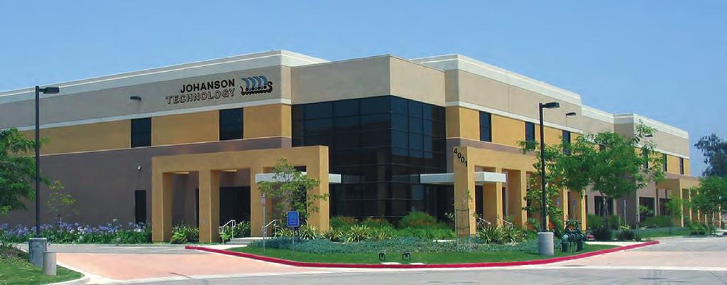
2 4001 Calle Tecate, Camarillo, California Tel (805) Fax (805)
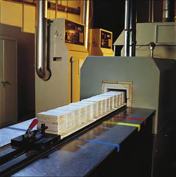
3 The mission of the Johanson companies is to translate our customer needs into quality electronic components, produced in factories that are models of excellence, supported by innovative service. With over 20 years of experience, Johanson Technology can provide both standard and custom technology solutions tailored to your specific RF/Microwave applications. Our software design tools, library of more than 20 dielectric materials and various metal systems, and our thin-film and thick-film manufacturing capabilities enable us to produce components that are ideally suited to your specific needs. Your Technology Partner CONTENTS Prototyping Kits JTISoft Capacitor & Inductor Modeling Software... 6 Multi-Layer High-Q Capacitors Monolithic Ceramic Chip Inductors Wire Wound Ceramic Chip Inductors Integrated Passive Component Overview Antennas Band Pass Filters High Pass Filters EMI Filters Low Pass Filters Directional Couplers Baluns & Balun Filters Diplexers Integrated Passive Component Case Size Drawings Custom LTCC Modules LASERtrim RF Tuning Capacitors Broadband Single Layer Capacitors Single Layer Microwave Capacitors Custom Substrates & Thin Film Products Chip Capacitor Packaging Information Chip Inductor & Wirewound Inductor Packaging Information Technical Notes List Additional application notes may be found on our web site. Johanson Technology s ISO 9001 Certified design and manufacturing operations are located in Camarillo, California. Our quality minded management system utilizes the latest in computerized SPC systems and continuous improvement programs focused on increased product reliability, manufacturing through-put, and production yields. Our broad experience, applications support, software libraries, and responsive service enhance our ability to drive down your total cost of procurement and speed your time to market. Johanson Technology, Inc. reserves the right to make design and price changes without notice. All sales are subject to the terms and conditions printed on the back side of our sales order acknowledgment forms including a limited warranty and remedies for non-conforming goods or defective goods. We will be pleased to provide a copy of these terms and conditions for your review. 3


4 RF Ceramic Component Proto-Typing Kits Johanson Technology s engineering prototype kits provide RF designers with a broad selection of high frequency ceramic components. Each kit contains a selection of components as well as the latest product data on Johanson s full line of High Frequency Ceramic Solutions. List price is $ each, but price may be waived for qualified high volume applications. The selections listed below represents typical kit contents. Johanson reserves the right to make limited value/tolerance substitutions when necessary. Please advise any critical values at time of order. Capacitor and Inductor Design Kits 0201 L-Series Capacitors & Ceramic Inductors (Values {pf or nh} & tolerances) P/N : L/C-201DL 50 PCS. EA. MLCC (pf): 0.3 B, 0.5 B, 0.7 B, 0.9 B, 1.0 B, 1.2 B, 1.5 B, 1.8 B, 2.2 B, 2.7 B, 3.0 B, 3.3 B, 3.6 B, 3.9 B, 4.3 B, 4.7 B, 5.1 C, 5.6 C, 6.8 C, 8.2 C, 9.1 C, 10 J, 12 J, 15 J, 18 J, 22 J, 27 J, 33 J 50 PCS. EA. MLCI (nh): 0.6 C, 0.8 C, 1.0 S, 1.2 S, 1.5 S, 1.8 S, 2.2 S, 2.4 S, 2.7 S, 3.0 S, 3.3 S, 3.7 S, 3.9 S, 4.7 S, 5.1 S, 5.6 S, 6.8 J, 8.2 J, 10 J, 12 J, 13 J, 15 J, 18 J, 20 J, 22 J, 27 J, 33 J, 39 J 0402 S-Series Capacitors & Ceramic Inductors (Values {pf or nh} & tolerances) P/N : L/C-402DS 50 PCS. EA. MLCC (pf): 0.2 B, 0.3 B, 0.5 B, 0.7 B, 0.9 B, 1.0 B, 1.2 B, 1.5 B, 1.8 B, 2.0 B, 2.2 B, 2.4 B, 2.7 B, 3.0 B, 3.6 B, 4.3 B, 4.7 B, 5.6 C, 6.8 C, 7.5 C, 8.2 C, 9.1 C, 10 J, 12 J, 15 J, 22 J, 27 J, 30 J 50 PCS. EA. MLCI (nh): 1.0 S, 1.2 S, 1.5 S, 1.8 S, 2.2 S, 2.4 S, 2.7 S, 3.0 S, 3.3 S, 3.9 S, 4.3 S, 4.7 S, 5.1 S, 5.6 S, 6.8 J, 7.5 J, 8.2 J, 10 J, 12 J, 15 J, 18 J, 22 J, 27 J, 33 J, 39 J, 47 J, 68 J, 100 J 0603 S-Series Capacitors & Ceramic Inductors (Values {pf or nh} & tolerances) P/N : L/C-603DS 50 PCS. EA. MLCC (pf): 0.3 B, 0.5 B, 0.8 B, 1.0 B, 1.2 B, 1.5 B, 1.8 B, 2.2 B, 2.7 B, 3.3 B, 3.6 B, 3.9 B, 4.7 B, 5.6 C, 6.8 C, 8.2 C, 10 J, 12 J, 15 J, 18 J, 20 J, 24 J, 27 J, 33 J, 39 J, 47 J, 68 J, 82 J 50 PCS. EA. MLCI (nh): 1.0 S, 1.5 S, 1.8 S, 2.2 S, 2.7 S, 3.3 S, 3.9 S, 4.7 S, 5.6 S, 6.8 J, 8.2 J, 10 J, 12 J, 15 J, 18 J, 22 J, 27 J, 33 J, 39 J, 47 J, 56 J, 68 J, 82 J, 100 J, 120 J, 150 J, 180 J, 220 J 0805 S-Series Capacitors & WireWound High Q Chip Inductors (Values {pf or nh} & tolerances) P/N : L/C-805DS 50 PCS. EA. MLCC (pf): 4.7 B, 5.6 C, 6.8 C, 7.5 C, 8.2 C, 9.1 C, 10 J, 12 J, 15 J, 18 J, 20 J, 22 J, 24 J, 27 J, 30 J, 33 J, 36 J, 39 J, 43 J, 47 J, 56 J, 68 J, 82 J, 100 J, 120 J, 150 J, 180 J, 220 J 20 PCS. EA. (nh): 2.7 C, 3.9 C, 5.6 C, 6.8 J, 8.2 J, 12 J, 16 J, 20 J, 27 J, 33 J, 39 J, 47 J, 56 J, 68 J, 82 J, 100 J, 120 J, 150 J, 180 J, 220 J, 270 J, 330 J, 390 J, 560 J, 1000 J, 2200 J, 6800 J, J Non-Magnetic Capacitor Designer Kit EIA 1111 S42E-Series Capacitors (Values {pf} & tolerances) Non-Magnetic P/N: S111DUE 10 PCS. EACH (pf): 1.0 B 3.9 B, 4.7 B, 6.8 C, 7.5 C, 8.2 C, 9.1 C, 10 J, 12 J, 15 J, 18 J, 20 J, 27 J, 33 J, 47 J, 56 J, 68 J, 82 J, 100 J, 120 J, 150 J, 180 J, 220 J, 270 J, 390 J, 470 J, 560 K, 1000 K 0201 L-Series Capacitors (Values {pf} & tolerances) P/N: S201TL 50 PCS. EACH (pf): 0.2 A, 0.3 A, 0.4 A, 0.5 B, 0.6 B, 0.7 B, 0.8 B, 0.9 B, 1.0 B, 1.1 B, 1.2 B, 1.3 B, 1.5 B, 1.8 B, 2.0 B, 2.2 B, 2.4 B, 2.7 B, 3.0 B, 3.3 B, 3.6 B, 3.9 B, 4.3 B, 4.7 B, 5.1 C, 5.6 C, 6.2 C, 6.8 C 0603 S-Series Capacitors (Values {pf} & tolerances) P/N: S603TS 50 PCS. EACH (pf): 0.2 B, 0.3 B, 0.4 B, 0.5 B, 0.6 B, 0.7 B, 0.8 B, 0.9 B, 1.0 B, 1.1 B, 1.2 B, 1.3 B, 1.5 B, 1.8 B, 2.0 B, 2.2 B, 2.4 B, 2.7 B, 3.0 B, 3.3 B, 3.6 B, 3.9 B, 4.3 B, 4.7 B, 5.1 C, 5.6 C, 6.2 C, 6.8 C 1111 E-Series Capacitors (Values {pf} & tolerances) P/N: S111TVE 10 PCS. EACH (pf): 0.5 B, 0.6 B, 0.7 B, 0.8 B, 0.9 B, 1.0 B, 1.1 B, 1.2 B, 1.3 B, 1.5 B, 2.0 B, 2.2 B, 2.4 B, 2.7 B, 3.0 B, 3.3 B, 3.6 B, 3.9 B, 4.3 B, 4.7 B, 5.1 C, 5.6 C, 6.2 C, 6.8 C, 7.5 C, 8.2 C, 9.1 C, 10 J Non-Magnetic Capacitor Tuning Kit Broadband Single Layer Capacitors 10 PCS. EACH: V01A151MT, V02A471MT, V02A102MT, V03A102MT, V04A182MT Tuning Capacitor Kits 0201 S-Series Ultra High-Q Capacitors (Values {pf} & tolerances) P/N: S201TS Contains 50 PCS. EACH of the following 0201 capacitor sizes (pf): 0.3 B, 0.5 B, 0.7 B, 0.9 B, 1.0 B, 1.2 B, 1.5 B, 1.8 B, 2.2 B, 2.7 B, 3.0 B, 3.3 B, 3.6 B, 3.9 B, 4.3 B, 4.7 B, 5.1 C, 5.6 C, 6.8 C, 8.2 C, 9.1 C, 10 J, 12 J, 15 J 0402 S-Series Capacitors (Values {pf} & tolerances) P/N: S402TS 50 PCS. EACH (pf): 0.2 A, 0.3 A, 0.4 A, 0.5 B, 0.6 B, 0.7 B, 0.8 B, 0.9 B, 1.0 B, 1.1 B, 1.2 B, 1.3 B, 1.5 B, 1.8 B, 2.0 B, 2.2 B, 2.4 B, 2.7 B, 3.0 B, 3.3 B, 3.6 B, 3.9 B, 4.3 B, 4.7 B, 5.1 C, 5.6 C, 6.2 C, 6.8 C 0805 S-Series Capacitors (Values {pf} & tolerances) P/N: S805TS 50 PCS. EACH (pf): 0.3 B, 0.5 B, 0.7 B, 0.9 B, 1.0 B, 1.1 B, 1.2 B, 1.3 B, 1.5 B, 1.8 B, 2.0 B, 2.2 B, 2.4 B, 2.7 B, 3.0 B, 3.3 B, 3.6 B, 3.9 B, 4.3 B, 4.7 B, 5.1 C, 5.6 C, 6.2 C, 6.8 C, 7.5 C, 8.2 C, 9.1 C, 10 J EIA 1111 S42E-Series Capacitors (Values {pf} & tolerances) Non-Magnetic Single Layer Capacitor Kits P/N: S111TUE 10 PCS. EACH (pf): 0.5 B, 0.6 B, 0.7 B, 0.8 B, 0.9 B, 1.0 B, 1.1 B, 1.2 B, 1.3 B, 1.5 B, 2.0 B, 2.2 B, 2.4 B, 2.7 B, 3.0 B, 3.3 B, 3.6 B, 3.9 B 4.3 B, 4.7 B, 5.1 C, 5.6 C, 6.2 C, P/N: GBBL 4
5 WireWound Tuning Capacitor Inductor Kits Kits 0402 WireWound High Q Chip Inductors (Values {nh} & tolerances) P/N: L402W 20 PCS. EACH (nh): 1.0 C, 1.8 C, 2.0 C, 2.7 C, 3.3 C, 3.9 C, 4.7 C, 5.6 C, 6.8 J, 7.5 J, 8.2 J, 9.0 J, 10 J, 12 J, 15 J, 18 J, 20 J, 22 J, 24 J, 27 J, 30 J, 33 J, 39 J, 47 J, 56 J, 82 J, 100 J, 120 J 0603 WireWound High Q Chip Inductors (Values {nh} & tolerances) P/N: L603W 20 PCS. EACH (nh): 1.6 C, 1.8 C, 2.0 C, 3.9 C, 4.7 C, 5.1 C, 5.6 C, 6.8 J, 7.5 J, 8.2 J, 10 J, 12 J, 15 J, 18 J, 22 J, 27 J, 33 J, 39 J, 47 J, 56 J, 68 J, 72 J, 82 J, 100 J, 150 J, 180 J, 270 J, 330 J 0805 WireWound High Q Chip Inductors (Values {nh} & tolerances) P/N: L805W 20 PCS. EACH (nh): 2.7 C, 3.9 C, 5.6 C, 6.8 J, 8.2 J, 12 J, 16 J, 20 J, 27 J, 33 J, 39 J, 47 J, 56 J, 68 J, 82 J, 100 J, 120 J, 150 J, 180 J, 220 J, 270 J, 330 J, 390 J, 560 J, 1000 J, 2200 J, 6800 J, J (Individual) Capacitor, Inductor Designer Kits 0201 L-Series Capacitors (Values {pf} & tolerances) P/N: S201DL 50 PCS. EACH (pf): 0.3 B, 0.5 B, 0.7 B, 0.9 B, 1.0 B, 1.2 B, 1.5 B, 1.8 B, 2.2 B, 2.7 B, 3.0 B, 3.3 B, 3.6 B, 3.9 B, 4.3 B, 4.7 B, 5.1 C, 5.6 C, 6.8 C, 8.2 C, 9.1 C, 10 J, 12 J, 15 J, 18 J, 22 J, 27 J, 33 J 0201 L-Series Ultra High-Q Capacitors Horizontal Electrode Orientation (Values {pf} & tolerances) P/N: S201LS Contains 50 PCS. EACH of the following 0201 capacitor sizes (pf): 0.3 B, 0.5 B, 0.7 B, 0.9 B, 1.0 B, 1.2 B, 1.5 B, 1.8 B, 2.2 B, 2.7 B, 3.0 B, 3.3 B, 3.6 B, 3.9 B, 4.3 B, 4.7 B, 5.1 C, 5.6 C, 6.8 C, 8.2 C, 9.1 C, 10 J, 12 J, 15 J 0201 L-Series Ultra High-Q Capacitors Verticle Electrode Orientation (Values {pf} & tolerances) P/N: S201VS Contains 50 PCS. EACH of the following 0201 capacitor sizes (pf): 0.3 B, 0.5 B, 0.7 B, 0.9 B, 1.0 B, 1.2 B, 1.5 B, 1.8 B, 2.2 B, 2.7 B, 3.0 B, 3.3 B, 3.6 B, 3.9 B, 4.3 B, 4.7 B, 5.1 C, 5.6 C, 6.8 C, 8.2 C, 9.1 C, 10 J, 12 J, 15 J 0201 Inductors (Values {nh} & tolerances) P/N: L201DC 50 PCS. EACH (nh): 0.6 C, 0.8 C, 1.0 S, 1.2 S, 1.5 S, 1.8 S, 2.2 S, 2.4 S, 2.7 S, 3.0 S, 3.3 S, 3.7 S, 3.9 S, 4.7 S, 5.1 S, 5.6 S, 6.8 J, 8.2 J, 10 J, 12 J, 13 J, 15 J, 18 J, 20 J, 22 J, 27 J, 33 J, 39 J 0402 S-Series Capacitors (Values {pf} & tolerances) P/N: S402DS 50 PCS. EACH (pf): 0.2 B, 0.3 B, 0.5 B, 0.7 B, 0.9 B, 1.0 B, 1.2 B, 1.5 B, 1.8 B, 2.0 B, 2.2 B, 2.4 B, 2.7 B, 3.0 B, 3.6 B, 4.3 B, 4.7 B, 5.6 C, 6.8 C, 7.5 C, 8.2 C, 9.1 C, 10 J, 12 J, 15 J, 22 J, 27 J, 30 J 0402 Inductors (Values {nh} & tolerances) P/N: L402DC 50 PCS. EACH (nh): 1.0 S, 1.2 S, 1.5 S, 1.8 S, 2.2 S, 2.4 S, 2.7 S, 3.0 S, 3.3 S, 3.9 S, 4.3 S, 4.7 S, 5.1 S, 5.6 S, 6.8 J, 7.5 J, 8.2 J, 10 J, 12 J, 15 J, 18 J, 22 J, 27 J, 33 J, 39 J, 47 J, 68 J, 100 J 0603 S-Series Capacitors (Values {pf} & tolerances) P/N: S603DS 50 PCS. EACH (pf): 0.3 B, 0.5 B, 0.8 B, 1.0 B, 1.2 B, 1.5 B, 1.8 B, 2.2 B, 2.7 B, 3.3 B, 3.6 B, 3.9 B, 4.7 B, 5.6 C, 6.8 C, 8.2 C, 10 J, 12 J, 15 J, 18 J, 20 J, 24 J, 27 J, 33 J, 39 J, 47 J, 68 J, 82 J 0603 Inductors (Values {nh} & tolerances) P/N: L603DC 50 PCS. EACH (nh): 1.0 S, 1.5 S, 1.8 S, 2.2 S, 2.7 S, 3.3 S, 3.9 S, 4.7 S, 5.6 S, 6.8 J, 8.2 J, 10 J, 12 J, 15 J, 18 J, 22 J, 27 J, 33 J, 39 J, 47 J, 56 J, 68 J, 82 J, 100 J, 120 J, 150 J, 180 J, 220 J 0805 S-Series Capacitors (Values {pf} & tolerances) P/N: S805DS 50 PCS. EACH (pf): 4.7 B, 5.6 C, 6.8 C, 7.5 C, 8.2 C, 9.1 C, 10 J, 12 J, 15 J, 18 J, 20 J, 22 J, 24 J, 27 J, 30 J, 33 J, 36 J, 39 J, 43 J, 47 J, 56 J, 68 J, 82 J, 100 J, 120 J, 150 J, 180 J, 220 J 1111 E-Series Capacitors (Values {pf} & tolerances) P/N: S111DVE 10 PCS. EACH (pf): 1.0 B, 3.9 B, 4.7 B, 6.8 C, 7.5 C, 8.2 C, 9.1 C, 10 J, 12 J, 15 J, 18 J, 20 J, 27 J, 33 J, 47 J, 56 J, 68 J, 82 J, 100 K, 120 K, 150 K, 180 K, 220 K, 270 K, 390 K, 470 K, 560 K, 1000 K 2.45GHz Designer Kit for WLAN, Bluetooth, Zigbee, ISM and S-Series Capacitors, 0402 Inductors & 2.45 GHz RF Components P/N: 2450L/C402D 6 PCS. EA. BAND PASS FILTERS: 2450BP07A100, 2450BP15B100 6 PCS. EA. CHIP ANTENNA: 2450AT18A100, 2450AT18B100, 2450AT42A100, 2450AT42B100, 2450AT43A100, 2450AT43B100, 2450AT45A100 6 PCS. EA. LOW PASS FILTER: 2450LP14A100, 2450LP14B100, 2450LP15A050 6 PCS. EA. HIGH PASS FILTER: 2450HP14A100 6 PCS. EA. BALUN: 2450BL14C050, 2450BL14C100, 2450BL15B050, 2450BL15B100, 2450BL15B200 6 PCS. EA. FILTER BALUN: 2450FB15A050, 2450FB39A050 6 PCS. EA. DIPLEXER: 2450DP15A5512, 2450DP15D PCS. EA. MLCC (pf): 0.3 B. 0.5 B. 1.0 B, 1.5 B, 1.8 B, 2.2 B, 2.7 B, 3.3 B, 3.9 B, 4.7 B, 5.6 C, 6.8 C, 8.2 C, 10 J 50 PCS. EA. MLCI (nh): 1.0 S,1.5 S, 1.8 S, 2.2 S, 2.7 S, 3.3 S, 4.7 S, 5.6 S, 6.8 J, 8.2 J, 10 J, 15 J, 18 J, 27 J 0603 S-Series Capacitors, 0603 Inductors & 2.45 GHz RF Components P/N: 2450L/C603D 6 PCS. EA. BAND PASS FILTERS: 2450BP07A100, 2450BP15B100 6 PCS. EA. CHIP ANTENNA: 2450AT18A100, 2450AT18B100, 2450AT42A100, 2450AT42B100, 2450AT43A100, 2450AT43B100, 2450AT45A100 6 PCS. EA. LOW PASS FILTER: 2450LP14A100, 2450LP14B100, 2450LP15A050 6 PCS. EA. HIGH PASS FILTER: 2450HP14A100 6 PCS. EA. BALUN: 2450BL14C050, 2450BL14C100, 2450BL15B050, 2450BL15B100, 2450BL15B200 6 PCS. EA. FILTER BALUN: 2450FB15A050, 2450FB39A050 6 PCS. EA. DIPLEXER: 2450DP15A5512, 2450DP15D PCS. EA. MLCC (pf): 0.3 B, 0.5 B, 1.0 B, 1.5 B, 1.8 B, 2.2 B, 2.7 B, 3.3 B, 3.9 B, 4.7 C, 5.6 C, 6.8 C, 8.2 C, 10 J 50 P CS. EA. MLCI (nh): 1.0 S, 1.5 S, 1.8 S, 2.2 S, 2.7 S, 3.3 S, 4.7 S, 5.6 S, 6.8 J, 8.2 J, 10 J, 15 J, 18 J, 27 J 5

: 1.0 S, 1.5 S, 1.8 S, 2.2 S, 2.7 S, 3.3 S, 3.9 S, 4.7 S, 5.6 S, 6.8 J, 8.")

6 5.5GHz Designer Kit for WLAN, Bluetooth, ISM and S-Series Capacitors, 0402 Inductors & RF Components P/N: 5500L/C402D 6 PCS. EA. BAND PASS FILTERS: 5515BP15C1020, 5515BP15B725, 5515BP15B730, 5515BP15C975, 5487BP15B675, 5487BP15C675 6 PCS. EA. CHIP ANTENNA: 2450AD46A5400, 5250AT43A200, 5400AT18A1000, 5775AT43A100 6 PCS. EA. LOW PASS FILTER 5515LP15A730 6 PCS. EA. BALUN: 5400BL15B050, 5400BL15B100, 5400BL15K050, 5512BL15B100, 5800BL15B100 6 PCS. EA. DIPLEXER: 2450DP15A5512, 2450DP15B5512, 2450DP15D5400, 2450DP15E PCS. EA. MLCC (pf): 0.3 B, 0.5 B, 0.8 B, 1.0 B, 1.2 B, 1.5 B, 1.8 B, 2.0 B, 2.2 B, 2.7 B, 3.3 B, 3.9 B, 4.7 B, 5.6 C 50 PCS. EA. MLCI (nh): 1.0 S, 1.5 S, 1.8 S, 2.2 S, 2.7 S, 3.3 S, 3.9 S, 4.7 S, 5.6 S, 6.8 J, 8.2 J, 10 J, 12 J, 15 J 0603 S-Series Capacitors, 0603 Inductors & RF Components P/N: 5500L/C603D 6 PCS. EA. BAND PASS FILTERS: 5515BP15C1020, 5515BP15B725, 5515BP15B730, 5515BP15C975, 5487BP15B675, 5487BP15C675 6 PCS. EA. CHIP ANTENNA: 2450AD46A5400, 5250AT43A200, 5400AT18A1000, 5775AT43A100 6 PCS. EA. LOW PASS FILTER 5515LP15A730 6 PCS. EA. BALUN: 5400BL15B050, 5400BL15B100, 5400BL15K050, 5512BL15B100, 5800BL15B100 6 PCS. EA. DIPLEXER: 2450DP15A5512, 2450DP15B5512, 2450DP15D5400, 2450DP15E PCS. EA. MLCC (pf): 0.3 B, 0.5 B, 0.8 B,1.0 B, 1.2 B,1.5 B, 1.8 B, 2.0 B, 2.2 B, 2.7 B, 3.3 B, 3.9 B, 4.7 B, 5.6 C 50 PCS. EA. MLCI (nh): 1.0 S, 1.5 S, 1.8 S, 2.2 S, 2.7 S, 3.3 S, 3.9 S, 4.7 S, 5.6 S, 6.8 J, 8.2 J, 10 J, 12 J, 15 J Designer Kit for WiMAX & UWB 0402 S-Series Capacitors, 0402 Inductors & RF Components P/N: WUWBL/C402D 6 PCS. EA. CHIP ANTENNA: 2500AT44M0400, 3100AT51A PCS. EA. LOW PASS FILTER 3550LP14A300 6 PCS. EA. BAND PASS FILTERS: 2500BP15M400, 3600BP15M600, 4000BP15U1800, 5130BP18U PCS. EA. BALUN: 2500BL14M050, 2450BL14M100, 3600BL14M050, 3600BL14M100, 4000BL14U100 6 PCS. EA. FILTER BALUN: 2345FB39A0050, 2595FB39A0050, 3500FB39A PCS. EA. MLCC (pf): 0.3 B. 0.5 B. 1.0 B, 1.5 B, 1.8 B, 2.2 B, 2.7 B, 3.3 B, 3.9 B, 4.7 B, 5.6 C, 6.8 C, 8.2 C, 10 J 50 PCS. EA. MLCI (nh): 1.0 S,1.5 S, 1.8 S, 2.2 S, 2.7 S, 3.3 S, 4.7 S, 5.6 S, 6.8 J, 8.2 J, 10 J, 15 J, 18 J, 27 J 0603 S-Series Capacitors, 0603 Inductors & RF Components P/N: WUWBL/C603D 6 PCS. EA. CHIP ANTENNA: 2500AT44M0400, 3100AT51A PCS. EA. LOW PASS FILTER 3550LP14A300 6 PCS. EA. BAND PASS FILTERS: 2500BP15M400, 3600BP15M600, 4000BP15U1800, 5130BP18U PCS. EA. BALUN: 2500BL14M050, 2450BL14M100, 3600BL14M050, 3600BL14M100, 4000BL14U100 6 PCS. EA. FILTER BALUN: 2345FB39A0050, 2595FB39A0050, 3500FB39A PCS. EA. MLCC (pf): 0.3 B. 0.5 B. 1.0 B, 1.5 B, 1.8 B, 2.2 B, 2.7 B, 3.3 B, 3.9 B, 4.7 B, 5.6 C, 6.8 C, 8.2 C, 10 J 50 PCS. EA. MLCI (nh): 1.0 S,1.5 S, 1.8 S, 2.2 S, 2.7 S, 3.3 S, 4.7 S, 5.6 S, 6.8 J, 8.2 J, 10 J, 15 J, 18 J, 27 J Standard Termination for all kits - 100% Sn. Consult Factory for other termination options JTIsoft 2.0 Capacitor & Inductor Modeling Software JTIsoft consists of two advanced design simulation software programs which offer component modeling from 1 MHz to 20 GHz. MLCsoft provides S-Parameter and SPICE modeling data for six different size high frequency multi-layer ceramic capacitors (MLCCs) chip sizes while MLIsoft provides S-Parameter and SPICE modeling on four different size high frequency multi-layer ceramic inductors (MLCIs). The main interface screen displays electrical parameters such as SRF, PRF1, PRF2, ESR, Q, Ceff, Leff, Rdc, and Idc which are updated dynamically as chip size, value, and frequency parameters are varied by the user. The complete part number is also dynamically displayed for ordering accuracy. Both programs also provide highly detailed graphical plots of device performance over a user specified frequency range. The chart displays are instantly updated as the user makes component or frequency changes. Smith chart displays of both impedance and S11/S22 are available as point plots, line plots, and line-point plots. Traditional X-Y graphs are available for parameters of S21 and S11 both phase and magnitude, Impedance magnitude, as well as Q, ESR and effective capacitance. Display formats include standard, log Y, and log/log. Chart may be exported in BMP or Metafile format. Numerical S-Parameter data may be displayed and exported as an.s2p format file. JTIsoft is available for download from our web site. 6
 capacitors give an ultra-high Q performance, and exhibit NP0 temperature characteristics.")
 capacitors give excellent high-q performance from HF to Microwave frequencies. Typical uses are high voltage, high current applications.")
. How to Order 252 S48 E 470 K V 4 E VOLTAGE (DC) 6R3 = 6.")
7 Multi-Layer High-Q Capacitors These lines of multilayer capacitors have been developed for High-Q and microwave applications. The S-Series (R03S, R07S, R14S, R15S) capacitors give an ultra-high Q performance, and exhibit NP0 temperature characteristics. The L-Series (R05L) capacitors give mid-high Q performance, and exhibit NP0 temperature characteristics. The E-Series (S42E, S48E, S58E) capacitors give excellent high-q performance from HF to Microwave frequencies. Typical uses are high voltage, high current applications. They are offered in chip (Ni barrier or Non-Magnetic Pt.-Ag) or in Non-Magnetic leaded form. The W-Series (R05W) capacitors offer a large capacitance value in an ultra-small 0201 package size. These exhibit a X7R temperature characteristic. RoHS compliance is standard for all unleaded parts (see termination options box). How to Order 252 S48 E 470 K V 4 E VOLTAGE (DC) 6R3 = 6.3 V 101 = 100 V 160 = 16 V 250 = 25 V 500 = 50 V 201 = 200 V 251 = 250 V 301 = 300 V 501 = 500 V 102 = 1000 V 152 = 1500 V 202 = 2000 V 252 = 2500 V 362 = 3600 V 502 = 5000 V 722 = 7200 V CASE SIZE R03 (01005) R05 (0201) R07 (0402) R14 (0603) R15 (0805) S42 (1111) S48 (2525) S58 (3838) CAPACITANCE (pf) 1st two digits are significant; third digit denotes number of zeros, R = decimal. 100 = 10 pf 101 = 100 pf DIELECTRIC S = Ultra High Q NPO L = High Q NPO E = Ultra High Q NPO, High Voltage, High Power, *T = High Temp (175C) Ultra High Q NPO W= X7R TOLERANCE A = ± 0.05 pf B = ± 0.10 pf C = ± 0.25 pf D = ± 0.50 pf F = ±1 % G = ±2% J = ±5% K = ± 10% For tolerance availability, see chart. TERMINATION Nickel Barrier V = Ni/Sn (Green) T = Ni/SnPb G = Ni/Au (Green) Non-Mag* U = Cu/Sn (Green) C = Cu/SnPb Leaded (All Non-Mag)* 1 = Microstrip 2 = Axial Ribbon 3 = Axial Wire 4 = Radial Ribbon 5 = Radial Wire Part Number written: 252S48E470KV4E MARKING 3 = Cap Code & Tolerance 4 = No Marking 6 = EIA Code (Marking on 0805 and larger only) PACKAGING S = Bulk W = Waffle Pack Y = Paper 5 Reel T = Paper 7 Reel *R = Paper 13 Reel *J = Paper 5 Reel - Horizontally Oriented Electrodes *N = Paper 5 Reel - Vertically Oriented Electrodes *L = Paper 7 Reel - Horizontally Oriented Electrodes *V = Paper 7 Reel - Vertically Oriented Electrodes Z = Embossed 5 Reel E = Embossed 7 Reel *U = Embossed 13 Reel *M = Embossed 5 Reel - Horizontally Oriented Electrodes *Q = Embossed 5 Reel - Vertically Oriented Electrodes *G = Embossed 7 Reel - Horizontally Oriented Electrodes *P = Embossed 7 Reel - Vertically Oriented Electrodes Tape specifications conform to EIA RS481 * - Not available for all MLCC - Call factory for info. 7
8 Low ESR / High-Q Capacitor Selection Chart Cap. Value EIA Size Miniature Size - Portable Electronics (R03S) 0201 (R05) 0402 NPO (R05L) X7R* (R05W) (R07S) 0603 (R14S) 0805 (R15S) RF Power Applications 0805 (R15E) 1111 (S42E) 2525 (S48E) 3838 (S58E) Capacitance pf Code Voltage 0.1 0R R2 16 V 25 V 50/200 V 250 V 500V 1000V 0.3 0R3 16 V 25 V 50/200 V 250 V 250 V 500V 500V 1000V 0.4 0R4 16 V 25 V 50/200 V 250 V 250 V 500V 500V 1000V 0.5 0R5 16 V 25 V 50/200 V 250 V 250 V 500V 500V 1000V 2500V 0.6 0R6 16 V 25 V 50/200 V 250 V 250 V 500V 500V 1000V 2500V 3600V 7200V 0.7 0R7 16 V 25 V 50/200 V 250 V 250 V 500V 500V 1000V 2500V 3600V 7200V 0.8 0R8 16 V 25 V 50/200 V 250 V 250 V 500V 500V 1000V 2500V 3600V 7200V 0.9 0R9 16 V 25 V 50/200 V 250 V 250 V 500V 500V 1000V 2500V 3600V 7200V 1.0 1R0 16 V 25 V 50/200 V 250 V 250 V 500V 500V 1000V 2500V 3600V 7200V 1.1 1R1 16 V 25 V 50/200 V 250 V 250 V 500V 500V 1000V 2500V 3600V 7200V 1.2 1R2 A 16 V 25 V 50/200 V 250 V 250 V 500V 500V 1000V 2500V 3600V 7200V 1.3 1R3 16 V 25 V 50/200 V 250 V 250 V 500V 500V 1000V 2500V 3600V 7200V 1.4 1R4 16 V 25 V 50/200 V 250 V 250 V 500V 500V 1000V 2500V 3600V 7200V 1.5 1R5 B 16 V 25 V 50/200 V 250 V 250 V 500V 500V 1000V 2500V 3600V 7200V 1.6 1R6 16 V 25 V 50/200 V 250 V 250 V 500V 500V 1000V 2500V 3600V 7200V 1.7 1R7 C 16 V 25 V 50/200 V 250 V 250 V 500V 500V 1000V 2500V 3600V 7200V 1.8 1R8 16 V 25 V 50/200 V 250 V 250 V 500V 500V 1000V 2500V 3600V 7200V 1.9 1R9 D 16 V 25 V 50/200 V 250 V 250 V 500V 500V 1000V 2500V 3600V 7200V 2.0 2R0 16 V 25 V 50/200 V 250 V 250 V 500V 500V 1000V 2500V 3600V 7200V 2.1 2R1 16 V 25 V 50/200 V 250 V 250 V 500V 500V 1000V 2500V 3600V 7200V 2.2 2R2 16 V 25 V 50/200 V 250 V 250 V 500V 500V 1000V 2500V 3600V 7200V 2.4 2R4 16 V 25 V 50/200 V 250 V 250 V 500V 500V 1000V 2500V 3600V 7200V 2.7 2R7 16 V 25 V 50 V 250 V 250 V 500V 500V 1000V 2500V 3600V 7200V 3.0 3R0 16 V 25 V 50 V 250 V 250 V 500V 500V 1000V 2500V 3600V 7200V 3.3 3R3 16 V 25 V 50 V 250 V 250 V 500V 500V 1000V 2500V 3600V 7200V 3.6 3R6 16 V 25 V 50 V 250 V 250 V 500V 500V 1000V 2500V 3600V 7200V 3.9 3R9 16 V 25 V 50 V 250 V 250 V 500V 500V 1000V 2500V 3600V 7200V 4.3 4R3 16 V 25 V 50 V 250 V 250 V 500V 500V 1000V 2500V 3600V 7200V 4.7 4R7 16 V 25 V 50 V 250 V 250 V 500V 500V 1000V 2500V 3600V 7200V 5.1 5R1 16 V 25 V 50 V 250 V 250 V 500V 500V 1000V 2500V 3600V 7200V 5.6 5R6 A** 16 V 25 V 50 V 250 V 250 V 500V 500V 1000V 2500V 3600V 7200V 6.2 6R2 16 V 25 V 50 V 250 V 250 V 500V 500V 1000V 2500V 3600V 7200V B 6.8 6R8 16 V 25 V 50 V 250 V 250 V 500V 500V 1000V 2500V 3600V 7200V 7.5 7R5 C 16 V 25 V 50 V 250 V 250 V 500V 500V 1000V 2500V 3600V 7200V 8.2 8R2 16 V 25 V 50 V 250 V 250 V 500V 500V 1000V 2500V 3600V 7200V D 9.1 9R1 16 V 25 V 50 V 250 V 250 V 500V 500V 1000V 2500V 3600V 7200V V 25 V 50 V 250 V 250 V 500V 500V 1000V 2500V 3600V 7200V V 25 V 50 V 250 V 250 V 500V 500V 1000V 2500V 3600V 7200V V 25 V 50 V 250 V 250 V 500V 500V 1000V 2500V 3600V 7200V F 16 V 25 V 50 V 250 V 250 V 500V 500V 1000V 2500V 3600V 7200V V 25 V 50 V 250 V 250 V 500V 500V 1000V 2500V 3600V 7200V G 16 V 25 V 50 V 250 V 250 V 500V 500V 1000V 2500V 3600V 7200V V 50 V 250 V 250 V 500V 500V 1000V 2500V 3600V 7200V V 50 V 250 V 250 V 500V 500V 1000V 2500V 3600V 7200V J V 50 V 250 V 250 V 500V 500V 1000V 2500V 3600V 7200V V 50 V 250 V 250 V 500V 500V 1000V 2500V 3600V 7200V K 25 V 50 V 250 V 250 V 500V 500V 1000V 2500V 3600V 7200V V 50 V 250 V 250 V 500V 500V 1000V 2500V 3600V 7200V V 50 V 250 V 250 V 500V 500V 1000V 2500V 3600V 7200V * The R05W parts, which are X7R, can only be provided with K or M tolerance. Consult factory for Non-Standard values. **A tolerance only available for R07S (0402) and R14S(0603) caps 8
9 Low ESR / High-Q Capacitor Selection Chart Cap. Value EIA Size Miniature Size - Portable Electronics (R03S) 0201 (R05) 0402 NPO (R05L) X7R* (R05W) (R07S) 0603 (R14S) 0805 (R15S) RF Power Applications 0805 (R15E) 1111 (S42E) 2525 (S48E) 3838 (S58E) Capacitance Tolerance pf Code Voltage V 250 V 250 V 500V 500V 1000V 2500V 3600V 7200V V 250 V 250 V 500V 500V 1000V 2500V 3600V 7200V V 250 V 250 V 500V 500V 1000V 2500V 3600V 7200V V 250 V 250 V 500V 500V 1000V 2500V 3600V 7200V V 250 V 250 V 500V 500V 1000V 2500V 3600V 7200V V 250 V 250 V 500V 500V 1000V 2500V 3600V 7200V V 250 V 250 V 500V 500V 1000V 2500V 3600V 7200V V 250 V 250 V 500V 500V 1000V 2500V 3600V 7200V V 250 V 250 V 500V 500V 1000V 2500V 3600V 7200V F 25 V 250 V 250 V 500V 500V 1000V 2500V 3600V 7200V V 250 V 250 V 500V 500V 1000V 2500V 3600V 7200V V 250 V 250 V 500V 500V 1000V 2500V 3600V 7200V G 16 V 250 V 300V 500V 2500V 3600V 7200V V 300V 500V 2500V 3600V 7200V J 250 V 300V 500V 2500V 3600V 7200V V 300V 500V 2500V 3600V 7200V K 250 V 300V 500V 2500V 3600V 7200V V 300V 500V 2500V 3600V 7200V V 300V 500V 2500V 3600V V 250 V 200V 500V 2500V 3600V V 500V 2500V 3600V V 500V 2500V 3600V V 500V 1500V 2500V V 500V 1500V 2500V V 500V 1500V 2500V V 500V 1500V 2500V V 500V 1500V 2500V V 200V 500V 1500V 2500V V 500V 1000V 2500V V 500V 1000V 2500V V 500V 1000V 2500V V 50V 1000V 2500V V 1000V 2500V V 50V 1000V 2500V G V 1000V 1000V V 50V 1000V 1000V J 1000V 1000V V 1000V K 500V 1000V V 300V 1000V V 500V V V V 500V V V * The R05W parts, which are X7R, can only be provided with K and M tolerance. Consult factory for Non-Standard values. 9
10 Dielectric Characteristics NPO X7R TEMPERATURE COEFFICIENT: QUALITY FACTOR / DF: INSULATION RESISTANCE: DIELECTRIC STRENGTH: 0 ± 30ppm / C, -55 to 125 C Q 1 MHz, Typical 10,000 > C,WVDC; 125 C IR is 10% of 25 C rating 500 V 2.5 X WVDC Min., 25 C, 50 ma max 1000 V 1.5 X WVDC Min., 25 C, 50 ma max > 1500 = 1 X WVDC Min., 25 C, 50 ma max ± 15%, -55 to 125 C 16VDC DF 1 KHz, 25 C 10VDC DF 1 KHz, 25 C >500 ΩF* or C,WVDC; 125 C IR is 10% of 25 C rating * whichever is less 2.5 X WVDC Min., 25 C, 50 ma max 1KHz ±50Hz, 1.0±0.2 VRMS, 25 C ,000 pf TEST PARAMETERS:: 1MHz ±50kHz, 1.0±0.2 VRMS, 25 C AVAILABLE CAPACITANCE: Size 01005: pf Size 0201: pf Size 0402: pf Size 0603: pf Size 0805: Size 1111: Size 2525: Size 3838: pf pf pf pf Mechanical & Environmental Characteristics SPECIFICATION TEST PARAMETERS SOLDERABILITY: Solder coverage 90% of metalized areas Preheat chip to C for 60 sec., dip terminals in rosin flux No termination degradation then dip in Sn ±5 C for 5±1 sec RESISTANCE TO No mechanical damage Preheat device to C for 60 sec. SOLDERING HEAT: Capacitance change: ±2.5% or 0.25pF followed by C for 60 sec. Q>500 I.R. >10 G Ohms Dip in 260 ±5 C solder for 10±1 sec. Breakdown voltage: 2.5 x WVDC Measure after 24±2 hour cooling period TERMINAL Termination should not pull off. Linear pull force* exerted on axial leads soldered to each terminal. ADHESION: Ceramic should remain undamaged. * lbs, lbs (min.) PCB DEFLECTION: No mechanical damage. Glass epoxy PCB: 0.5 mm deflection Capacitance change: 2% or 0.5pF Max LIFE TEST: MIL-STD-202, Method 108l Applied voltage: 120% of WDVC for capacitors rated at 500 volts DC or less. No mechanical damage 100% of WDVC for capacitors rated at 1250 volts DC or less. Capacitance change: ±3.0% or 0.3 pf Temperature: 125 ±3 C Q>500 I.R. >1 G Ohms Test time: hours Breakdown voltage: 2.5 x WVDC THERMAL CYCLE: No mechanical damage. 5 cycles of: 30± /-3 C, Capacitance change: ±2.5% or 0.25pF C, 30± /-0 C, Q>2000 I.R. >10 G Ohms C Breakdown voltage: 2.5 x WVDC Measure after 24±2 hour cooling period HUMIDITY, No mechanical damage. Relative humidity: 90-95% STEADY STATE: Capacitance change: ±5.0% or 0.50pF max. Temperature: 40 ±2 C Q>300 I.R. 1 G-Ohm Test time: /-0 Hours Breakdown voltage: 2.5 x WVDC Measure after 24±2 hour cooling period HUMIDITY, No mechanical damage. Applied voltage: 1.5 VDC, 50 ma max. LOW VOLTAGE: Capacitance change: ±5.0% or 0.50pF max. Relative humidity: 85±2% Temperature: 40 ±2 C Q>300 I.R. = 1 G-Ohm min. Test time: /-0 Hours Breakdown voltage: 2.5 x WVDC Measure after 24±2 hour cooling period VIBRATION: No mechanical damage. Capacitance change: ±2.5% or 0.25pF Cycle performed for 2 hours in each of three perpendicular directions Q>1000 I.R. 10 G-Ohm Frequency range 10Hz to 55 Hz to 10 Hz traversed Breakdown voltage: 2.5 x WVDC in 1 minute. Harmonic motion amplitude: 1.5mm 10
 mm (0.60 ±0.03) (0.30 ±0.03) (0.30 ±0.03) (0.20 Max.) 0402 In.040 ±.004.020 ±.004.020 ±.004.010 ±.006 (1005) mm (1.02 ±0.1) (0.51 ±0.1) (0.51 ±0.1) (0.25 ±.15) 0603 In.")
11 Mechanical Characteristics Size Units Length Width Thickness End Band In.016 ± ± ± Max. (0402) mm (0.40 ±0.03) (0.20 ±0.03) (0.20 ±0.03) (0.15 Max.) 0201 In.024 ± ± ± Max. (0603) mm (0.60 ±0.03) (0.30 ±0.03) (0.30 ±0.03) (0.20 Max.) 0402 In.040 ± ± ± ±.006 (1005) mm (1.02 ±0.1) (0.51 ±0.1) (0.51 ±0.1) (0.25 ±.15) 0603 In.062 ± ± / ±.006 (1608) mm (1.57 ±0.15) (0.81 ±0.15) ( ) (0.35 ±.15) 0805 In.080 ± ± ± ±.010 (2012) mm (2.03 ±0.20) (1.27 ±0.20) (1.02 ±.15) (0.50 ±.25) Horizontal and Verticle Oriented Capacitors Horizontal Electrode Orientation Vertical Electrode Orientation Applications & Features Size: EIA 0201, 0402 Performance: SRF s up to 20 GHz, Ultra High Q, Tight tolerance, Ultralow ESR Termination: Ni/Au, Ni/Sn, Ni/SnPb Applications: High Frequency Wireless Communications, Portable Wireless Products, Battery Powered Products RoHS Compliant Benifits of using Oriented Capacitors Consistent Orientation - Improved repeatability of production circuits. Consistent Orientation - More consistent filter performance. Vertical Orientation - The elimination of parallel frequencies. Vertical Orinetation - Lower inductance for a given capacitor. Horizontal Orientation - Lower coupling between adjacent capacitors. 11
12 E-Series Terminations and Leads Termination Size Units L Tol W Tol T E / B Tol In / Max Typ. +/ S42E mm / Max Typ. +/ V,T In / Max Typ. S48E U,C mm / Max Typ. In / Max Typ. S58E mm / Max Typ. For all E-Series Models: OPERATING TEMP. : -55 to +125 C INSULATION RESISTANCE: >1000 ΩF or >10 GΩ, whichever is 25 C WVDC TEMPERATURE COEFFICIENT: 0 ± 30ppm / C, -55 to 125 C DISSIPATION FACTOR (TYP.): < 1 MHz Unleaded Termination Codes V (Ni/Sn), T (Ni/SnPb), U (Cu/Sn non-mag), C (Cu/SnPb non-mag) Microstrip Ribbon Leads (Non-Magnetic), Termination Code 1 e Axial Ribbon Leads (Non-Magnetic), Termination Code 2 e W T T L E/B X W X W T LL L LL LL L LL Axial Wire Leads (Non-Magnetic), Termination Code 3 Radial Ribbon Leads (Non-Magnetic), Termination Code 4 Radial Wire Leads (Non-Magnetic), Termination Code 5 LL L LL L L T W T T W x W e LL LL x Lead Size Units L Tol W Tol T (max) E/B (typ) LL(min) X Tol e Tol In / / / / S42E mm / / / / In / / / / S48E mm / / / / In / / MAX / / S58E mm / / MAX / / In / / / / S42E mm / / / / In / / / / S48E mm / / / / In / / MAX / / S58E mm / / MAX / / S42E S48E In / / #26 AWG,.016 (.406) dia. nominal S58E mm / / S42E S48E In / / / / S58E mm / / / / S42E S48E In / / #26 AWG,.016 (.406) dia. nominal S58E mm / /
13 Series Resonance Chart 25.0 Typical Series Resonant Frequency (Series Mounted) 10.0 Frequency (GHz) 1.0 R05/0201 R07/0402 R14/0603 R15/ Capacitance (pf) RF Characteristics - L-Series ESR vs Frequency: 0201/R05L Q vs Frequency: 0201/R05L ESR (Ohms) pf 1.2 pf 3.3 pf 5.6 pf 8.2 pf 22 pf Q pf 1.2 pf 3.3 pf 8.2 pf 5.6 pf 22 pf Frequency (MHz) Frequency (MHz) ESR vs Capacitance: 0201/R05L Q vs Capacitance: 0201/R05L ESR (Ohms) MHz MHz MHz MHz Q MHz MHz MHz MHz Capacitance (pf) Capacitance (pf) 13
14 S-Series RF Characteristics versus Frequency Equivalent Series Resistance: 0402/R07S Q Factor: 0402/R07S ESR (Ohms) pf 4.7 pf 10 pf 1.2 pf 8.2 pf 15 pf Frequency (MHz) Q pf 4.7 pf 1.2 pf 8.2 pf 10 pf 15 pf Frequency (MHz) Equivalent Series Resistance: 0603/R14S Q Factor: 0603/R14S ESR (Ohms) pf 10 pf 15 pf 33 pf 47 pf H Q pf 10 pf 15 pf 33 pf 47 pf Frequency (MHz) Frequency (MHz) Equivalent Series Resistance: 0805/R15S Q Factor: 0805/R15S pf 15 pf 47 pf 100 pf 220pF pF 15pF 47pF 100pF 220pF 1000 ESR (Ohms) 0.1 Q Frequency (Mhz) Frequency (MHz) Measurements performed on a Boonton 34A Resonant Coaxial Line and represent typical capacitor performance. 14
15 S-Series RF Characterisitcs versus Capacitance Equivalent Series Resistance: 0402/R07S Q Factor: 0402/R07S ESR (Ohms) MHz MHz MHz MHz Capacitance (pf) Q MHz MHz MHz MHz Capacitance (pf) Equivalent Series Resistance: 0603/R14S Q Factor: 0603/R14S MHz MHz MHz MHz 1000 ESR (Ohms) 0.1 Q MHz MHz Capacitance (pf) MHz MHz Capacitance (pf) Equivalent Series Resistance: 0805/R15S Q Factor: 0805/R15S MHz MHz MHz MHz MHz MHz MHz MHz 1000 ESR (Ohms) 0.1 ESR (Ohms) Capacitance (pf) Capacitance (pf) Measurements performed on a Boonton 34A Resonant Coaxial Line and represent typical capacitor performance. 15
16 S42E Series RF Characteristics versus Frequency 1 Equivalent Series Resistance: 1111/S42E Q Factor: 1111/S42E 1.5pF 3.9pF 9.1pF 15pF 27pF 82pF 1000 ESR (Ohms) 0.1 Q pF 3.9pF 9.1pF 15pF 27pF 82pF Frequency (MHz) Frequency (MHz) S42E Series RF Characteristics versus Capacitance S42E Equivalent Series Resistance vs Capacitance, Typical S42E Q vs. Capacitance, Typical MHz MHz MHz ESR (Ohms) 0.1 Q MHz MHz MHz Capacitance (pf) Capacitance (pf) 10 S42E SRF (Series Mount), Typical JTI S42E SRF (GHz) Frequency Capacitance (pf) 16
17 JTI S48E Graphical Data 10 SRF (Shunt Mount), S48E, Typical (Preliminary) JTI S48E SRF Current Rating vs. Capacitance, S48E, Typical (Preliminary) 100 Frequency (GHz) 1 Current Rating (amps) MHz 64 MHz 128 MHz Capacitance (pf) As measured on a 8720C VNA, using a Shunt- Through fixture, and using the S11 magnitude dip to determine the SRF Capacitance (pf) Solid traces show voltage limited current (Vrms) Dotted traces show power dissipation limited current (Based on 4 Watts Power Dissipation, and 125 degrees C case temp.) S48E Q vs. Capacitance, Typical (Preliminary) S48E ESR vs. Capacitance, Typical (Preliminary) Q 1000 ESR (ohms) Q vs 64 MHz Q vs 128 MHz Capacitance (pf) ESR vs. 64 MHz ESR vs. 128 MHz Capacitance (pf) As measured on a 4287A LCR meter, using a 16092A fixture As measured on a 4287A LCR meter, using a 16092A fixture 17
18 JTI S48E Graphical Data S48E (EIA 2525) 12pF* (ESR vs. Freq) ESR (Ohms) S48E Frequency (MHz) *Actual data from Boonton 34A resonant line. JTI S58E Graphical Data S58E (EIA 3838) 47pF* (ESR vs. Freq) ESR (Ohms) S Frequency (MHz) *Actual data from Boonton 34A resonant line. 18

19 RF Ceramic Chip Inductors High frequency multi-layer chip inductors feature a monolithic body made of low loss ceramic and high conductivity metal electrodes to achieve optimal high frequency performance. These RF chip inductors are compact in size and feature lead-free tin plated nickel barrier terminations and tape and reel packaging which makes them ideal for small size/high volume wireless applications. Polarity Half-Marked Inductors (0201 only) Applications & Features CELL/PCS Modules Wireless LAN Broadband Components RFID RF Tranceivers RoHS Compliant (Standard, V Code) Sn/Pb Terminations Optional ( T Code) Product Range Summary EIA SIZE (mm) SIZE CODE L RANGE Q FACTOR (Min.) SRF (Typ.) TEMPERATURE 0201 (0603) L nh 4 (100 MHz) >21 GHz (1.0 nh) -40 C to +100 C 0402 (1005) L nh 8 (100 MHz) >21 GHz (1.0 nh) -40 C to +100 C 0603 (1608) L nh 12 (100 MHz) >23 GHz (1.0 nh) -40 C to +100 C Mechanical Characteristics Length Width Thickness End Band 0201 (0603) Inches mm.024 ±.001 (0.6 ±0.03).012 ±.001 (0.3 ±0.03).012 ±.001 (0.3 ±0.03).006 ±.002 (0.15 ±0.05) 0402 (1005) Inches mm.039 ±.004 (1.00 ±.10).020 ±.004 (0.50 ±.10).020 ±.004 (0.50 ±.10).009 ±.004 (0.23 ±.10) 0603 (1608) Inches mm.063 ±.006 (1.60 ±.15).031 ±.006 (0.80 ±.15).031 ±.006 (0.80 ±.15).012 ±.008 (0.30 ±.20) L E/B W T E/B How to Order L- 07 C 10N J V 6 T DEVICE Inductor SIZE 05 = = = 0603 Orientation Full Marking (all 0402) TYPE B = Polarity Half-Marked (all 0201) C = 0402 and 0603 (see Marking ) VALUE See Table TOLERANCE C = ± 0.2 nh 1.0 nh S = ± 0.3 nh 1.0 to 5.6 nh J = ± 5% 6.8 nh and above K = ± 10% 3.3 nh and above TERMINATION V = Ni/Sn T = Ni / SnPb Part number written: L-07C10NJV6T MARKING 4 = No Marking (all 0603) 6 = Orientation Mark (all 0201 and 0402*) PACKAGING Tape and Reel Size Code Tape Reel Qty 0201 T Paper 7 15, T Paper 7 10, T Paper 7 4,000 Bulk (Loose Pcs.) Size Code All S *Please note that all 0402 inductors (L-07C) have orientation full marking only. 19
20 RF Chip Inductor Selection Chart 0201 (L-05) 0402 (L-07) 0603 (L-14) EIA Size Inductor Value Inductance Tolerance nh Code 0.6 0N6 300 ma 0.7 0N7 300 ma 0.8 0N8 300 ma C 0.9 0N9 300 ma 1.0 1N0 300 ma 300 ma 300 ma (S only) 1.2 1N2 S 300 ma 300 ma (S only) 300 ma (S only) 1.3 1N3 300 ma 1.5 1N5 300 ma 300 ma (S only) 300 ma (S only) 1.8 1N8 300 ma 300 ma 300 ma 1.9 1N9 300 ma 300 ma 2.0 2N0 300 ma 300 ma 2.2 2N2 300 ma 300 ma 300 ma 2.3 2N3 S 300 ma 2.4 2N4 300 ma 300 ma 2.5 2N5 300 ma 2.7 2N7 300 ma 300 ma 300 ma 3.0 3N0 300 ma 300 ma 3.3 3N3 300 ma 300 ma 300 ma 3.6 3N6 300 ma 300 ma 3.7 3N7 300 ma K 3.9 3N9 300 ma 300 ma 300 ma 4.3 4N3 300 ma 4.7 4N7 S 300 ma 300 ma 300 ma 5.1 5N1 300 ma 300 ma 5.6 5N6 300 ma 300 ma 300 ma 6.2 6N2 300 ma 6.8 6N8 250 ma 250 ma 300 ma 7.5 7N5 250 ma 8.2 8N2 250 ma 250 ma 300 ma 10 10N 250 ma 250 ma 300 ma 12 12N 250 ma 250 ma 300 ma 13 13N 250 ma 250 ma 15 15N 250 ma 250 ma 300 ma 18 18N 200 ma 200 ma 300 ma 20 20N 200 ma 200 ma 22 22N 200 ma 200 ma 300 ma 23 23N 200 ma 27 27N 200 ma 200 ma 300 ma 33 33N 200 ma 200 ma 300 ma 39 39N 200 ma 150 ma 300 ma J 43 43N 150 ma 47 47N 150 ma 300 ma 56 56N K 150 ma 300 ma 68 68N 100 ma 300 ma 82 82N 100 ma 300 ma 100 R ma 300 ma 120 R ma 300 ma 150 R ma 180 R ma 220 R ma 270 R R R R R R68 Consult factory for Non-Standard values. See web page for Chip Inductor Product Detail Summary by part number 20
21 RF Characteristics Characteristics (Typical) INDUCTANCE VS FREQUENCY: SIZE 0201 Q VS FREQUENCY: SIZE N5 Inductance (nh) N 22N 10N 6N8 Q N 10N 6N8 3N3 3N3 1N Frequency (GHz) 33N Frequency (GHz) INDUCTANCE VS FREQUENCY: SIZE 0402 Q VS FREQUENCY: SIZE Inductance (nh) N 27N 15N 10 6N8 3N3 1N Frequency (GHz) Q 1N N3 6N N 20 27N 47N Frequency (GHz) (GHz) INDUCTANCE VS FREQUENCY: SIZE 0603 Q VS FREQUENCY: SIZE N2 80 Inductance (nh) R10 56N 27N 12N 4N7 2N2 Q R10 56N 27N 12N 4N Frequency (GHz) Frequency (GHz) (GHz) 21

22 RF Wirewound Chip Inductors These high frequency High-Q chip inductors feature a monolithic body made of low loss ceramic wound with wire to achieve optimal high frequency performance. These RF chip inductors are compact in size and are provided on tape and reel packaging which makes them ideal for high volume RF applications. They feature a nickel barrier with a top plating of gold for the ceramic core types (all 0402, all 0603, and most 0805 types), and with a top plating of 100% tin for the ferrite core types (0805 size, 470 nh and higher). Most inductance values between those listed are available on request. Applications Product Range Summary CELL/PCS Modules Broadband Components RF Tranceivers Cable Modem Bluetooth Wireless LAN RFID Cordless Phone Computer Peripherals ASDL EIA SIZE (mm) SIZE CODE L RANGE Q FACTOR (Typ.) SRF (Typ.) TEMPERATURE 0402 (1005) L nh 55 (900 MHz) >11 GHz (1.0 nh) -40 C to C 0603 (1608) L nh 60 (900 MHz) >13 GHz (2.0 nh) -40 C to C 0805 (2012) L ,000 nh 60 (500 MHz) >11 GHz (2.2 nh) -40 C to C* Mechanical Characteristics L W S T Length Width Thickness End Band 0402 (1005) Inches mm.039 ±.004 (1.00 ±.10).022 ±.004 (0.55 ±.10).020 ±.004 (0.50 ±.10).008 ±.004 (0.20 ±.10) *-40 deg. C to +85 deg. C for ferrite core types 0603 (1608) Inches mm.063 ±.008 (1.60 ±.20).041 ±.008 (1.05 ±.20).041 ±.008 (1.05 ±.20).014 ±.004 (0.35 ±.10) 0805 (2012) Inches mm.079 ±.008 (2.00 ±.20).049 ±.008 (1.25 ±.20).047 ±.008 (1.20 ±.20).016 ±.004 (0.40 ±.10) How to Order L- 07 W 4N3 S V 4 T DEVICE Inductor SIZE 07 = = = 0805 TYPE W = Wirewound on Ceramic Core F = Wirewound on Ferrite Core VALUE See Table TOLERANCE* C = ± 0.2 nh S = ± 0.3 nh G = ± 2% J = ± 5% K = ± 10% TERMINATION V = Ni / Au for W types, and V = Ni / 100% Sn for F types Example Part Number: L-07W4N3SV4T is: 0402 Wirewound, 4.3 nanohenry, +/- 0.3 nh tolerance, Ni / Au termination, No Marking, Paper tape on a 7 reel. MARKING 4 = No Marking PACKAGING Tape and Reel Size Code Tape Reel Qty 0402 T Paper 7 10, E Embossed 7 3, E Embossed 7 2,000 Bulk (Loose Pcs.) Size Code All S * See selection chart on the following pages for available tolerances of each value. 22
23 RF Wirewound Chip Inductor Selection Chart Inductor Value EIA Size 0402 (L-07) 0603 (L-14) 0805 (L-15) See web page for WireWound Inductor Product Detail Summary by part number Core Type CERAMIC CORE ( VV Type) EIA Size Inductor Value Inductance nh Code 0402 (L-07) 0603 (L-14) 0805 (L-15) Core Type Inductance Tolerance Rated Toler- Rated Toler- Rated nh Code Current ance Current ance Current 1.0 1N0 C, S 1360 ma 1.2 1N2 C, S 1300 ma 1.6 1N6 C, S 700 ma 1.8 1N8 C, S 1040 ma C, S 700 ma 1.9 1N9 C, S 1040 ma 2.0 2N0 C, S 1040 ma C, S 700 ma 2.2 2N2 C, S 960 ma C, S 800 ma 2.4 2N4 C, S 790 ma 2.6 2N6 C, S 640 ma 2.7 2N7 C, S 640 ma C, S 800 ma 3.3 3N3 C, J, K 840 ma C, S 700 ma C, S 800 ma 3.6 3N6 C, J, K 840 ma C, S 700 ma 3.9 3N9 C, J, K 840 ma C, S 700 ma C, S 600 ma 4.3 4N3 C, J, K 700 ma C, S 700 ma 4.7 4N7 C, J, K 640 ma C, S 700 ma C, S 600 ma 5.1 5N1 C, J, K 800 ma C, J, K 700 ma 5.6 5N6 C, J, K 760 ma C, J, K 700 ma C, J, K 600 ma 6.2 6N2 C, J, K 760 ma 6.8 6N8 C, J, K 680 ma C, J, K 700 ma C, G J, K 600 ma 7.5 7N5 C, J, K 680 ma C, J, K 700 ma J, K 600 ma 8.2 8N2 C, J, K 680 ma C, J, K 700 ma C, G, J, K 600 ma 8.7 8N7 C, J, K 480 ma C, J, K 700 ma 9.0 9N0 C, J, K 680 ma 9.5 9N5 C, J, K 680 ma C, J, K 700 ma 10 10N G, J, K 480 ma G, J, K 700 ma G, J, K 600 ma 11 11N G, J, K 640 ma G, J, K 700 ma 12 12N G, J, K 640 ma G, J, K 700 ma G, J, K 600 ma 13 13N G, J, K 560 ma J, K 600 ma 15 15N G, J, K 560 ma G, J, K 700 ma G, J, K 600 ma 16 16N G, J, K 560 ma G, J, K 700 ma G, J, K 600 ma 18 18N G, J, K 420 ma G, J, K 700 ma G, J, K 600 ma 19 19N G, J, K 480 ma 20 20N G, J, K 420 ma G, J, K 700 ma G, J, K 600 ma 22 22N G, J, K 400 ma G, J, K 700 ma G, J, K 600 ma 23 23N G, J, K 400 ma G, J, K 700 ma 24 24N G, J, K 400 ma G, J, K 700 ma J, K 600 ma 27 27N G, J, K 400 ma G, J, K 600 ma G, J, K 600 ma 30 30N G, J, K 400 ma G, J, K 700 ma 33 33N G, J, K 400 ma G, J, K 600 ma G, J, K 500 ma 36 36N G, J, K 320 ma J, K 600 ma 39 39N G, J, K 320 ma G, J, K 600 ma G, J, K 500 ma 40 40N G, J, K 320 ma 43 43N G, J, K 100 ma G, J, K 700 ma J, K 600 ma 47 47N G, J, K 100 ma G, J, K 600 ma G, J, K 500 ma 51 51N J, K 100 ma G, J, K 600 ma J, K 600 ma 56 56N J, K 100 ma G, J, K 600 ma G, J, K 500 ma 68 68N J, K 100 ma G, J, K 600 ma G, J, K 500 ma 72 72N G, J, K 400 ma 82 82N J, K 100 ma G, J, K 400 ma G, J, K 500 ma 100 R10 J, K 100 ma G, J, K 400 ma G, J, K 500 ma 110 R11 J, K 100 ma 120 R12 J, K 100 ma G, J, K 300 ma G, J, K 500 ma 150 R15 G, J, K 280 ma G, J, K 400 ma 180 R18 G, J, K 240 ma G, J, K 400 ma 220 R22 G, J, K 200 ma G, J, K 400 ma 270 R27 G, J, K 170 ma G, J, K 350 ma Tolerance Rated Current Tolerance Rated Current Tolerance Rated Current 330 R33 J, K 150 ma G, J, K 300 ma Ceramic 390 R39 J, K 100 ma G, J, K 210 ma 470 R47 J, K 100 ma J, K 500 ma 560 R56 J, K 450 ma 680 R68 J, K 400 ma 820 R82 J, K 300 ma R0 J, K 180 ma R2 J, K 150 ma R5 J, K 130 ma R8 J, K 120 ma R2 J, K 110 ma R7 J, K 100 ma R3 J, K 210 ma R9 J, K 200 ma R7 J, K 180 ma R6 J, K 160 ma R8 J, K 130 ma R2 J, K 120 ma R J, K 80 ma Consult factory for Non-Standard values. FERRITE CORE ( F Type) 23
24 RF Characteristics Characteristics (Typical) Q Q vs Frequency for 0402 Size 2.2 nh 3.3 nh 5.6 nh 8.2 nh 15 nh 36 nh Frequency (MHz) Inductance (nh) L vs Frequency for 0402 Size 2.2 nh 3.3 nh 5.6 nh 8.2 nh 15 nh 36 nh Frequency (MHz) Q Q vs Frequency for 0603 Size 2.0 nh 10 nh 22 nh 100 nh 180 nh Inductance (nh) L vs Frequency for 0603 Size 2.0nH 10 nh 22 nh 100 nh 180 nh Frequency (MHz) Frequency (MHz) Q Q vs Frequency for 0805 Size 2.7nH 27.0nH 100nH 270nH 470nH 680nH Frequency (MHz) Inductance (nh) L vs Frequency for 0805 Size nH 27.0nH nH 270nH nH 680nH Frequency (MHz) 24
25 0402 Inductance Range / Electrical Characteristics Part Number (Standard Tol.) 250MHz Availiable 250MHz Q 250MHz Q 900MHz Q 1.8GHz SRF (min.) DC Resistance (max.) Rated Current L-07W1N0SV4T 1.0 nh ±0.2 nh, ±0.3 nh GHz Ω 1360 ma L-07W1N2SV4T 1.2 nh ±0.2 nh, ±0.3 nh GHz Ω 1300 ma L-07W1N8SV4T 1.8 nh ±0.2 nh, ±0.3 nh GHz Ω 1040 ma L-07W1N9SV4T 1.9 nh ±0.2 nh, ±0.3 nh GHz Ω 1040 ma L-07W2N0SV4T 2.0 nh ±0.2 nh, ±0.3 nh GHz Ω 1040 ma L-07W2N2SV4T 2.2 nh ±0.2 nh, ±0.3 nh GHz Ω 960 ma L-07W2N4SV4T 2.4 nh ±0.2 nh, ±0.3 nh GHz Ω 790 ma L-07W2N7SV4T 2.7 nh ±0.2 nh, ±0.3 nh GHz Ω 640 ma L-07W3N3JV4T 3.3 nh ±0.2 nh, ±5%, ±10% GHz Ω 840 ma L-07W3N6JV4T 3.6 nh ±0.2 nh, ±5%, ±10% GHz Ω 840 ma L-07W3N9JV4T 3.9 nh ±0.2 nh, ±5%, ±10% GHz Ω 840 ma L-07W4N3JV4T 4.3 nh ±0.2 nh, ±5%, ±10% GHz Ω 700 ma L-07W4N7JV4T 4.7 nh ±0.2 nh, ±5%, ±10% GHz Ω 640 ma L-07W5N1JV4T 5.1 nh ±0.2 nh, ±5%, ±10% GHz Ω 800 ma L-07W5N6JV4T 5.6 nh ±0.2 nh, ±5%, ±10% GHz Ω 760 ma L-07W6N2JV4T 6.2 nh ±0.2 nh, ±5%, ±10% GHz Ω 760 ma L-07W6N8JV4T 6.8 nh ±0.2 nh, ±5%, ±10% GHz Ω 680 ma L-07W7N5JV4T 7.5 nh ±0.2 nh, ±5%, ±10% GHz Ω 680 ma L-07W8N2JV4T 8.2 nh ±0.2 nh, ±5%, ±10% GHz Ω 680 ma L-07W8N7JV4T 8.7 nh ±0.2 nh, ±5%, ±10% GHz Ω 480 ma L-07W9N0JV4T 9.0 nh ±0.2 nh, ±5%, ±10% GHz Ω 680 ma L-07W9N5JV4T 9.5 nh ±0.2 nh, ±5%, ±10% GHz Ω 680 ma L-07W10NJV4T 10.0 nh ±2%, ±5%, ±10% GHz Ω 480 ma L-07W11NJV4T 11.0 nh ±2%, ±5%, ±10% GHz Ω 640 ma L-07W12NJV4T 12.0 nh ±2%, ±5%, ±10% GHz Ω 640 ma L-07W13NJV4T 13.0 nh ±2%, ±5%, ±10% GHz Ω 560 ma L-07W15NJV4T 15.0 nh ±2%, ±5%, ±10% GHz Ω 560 ma L-07W16NJV4T 16.0 nh ±2%, ±5%, ±10% GHz Ω 560 ma L-07W18NJV4T 18.0 nh ±2%, ±5%, ±10% GHz Ω 420 ma L-07W19NJV4T 19.0 nh ±2%, ±5%, ±10% GHz Ω 480 ma L-07W20NJV4T 20.0 nh ±2%, ±5%, ±10% GHz Ω 420 ma L-07W22NJV4T 22.0 nh ±2%, ±5%, ±10% GHz Ω 400 ma L-07W23NJV4T 23.0 nh ±2%, ±5%, ±10% GHz Ω 400 ma L-07W24NJV4T 24.0 nh ±2%, ±5%, ±10% GHz Ω 400 ma L-07W27NJV4T 27.0 nh ±2%, ±5%, ±10% GHz Ω 400 ma L-07W30NJV4T 30.0 nh ±2%, ±5%, ±10% GHz Ω 400 ma L-07W33NJV4T 33.0 nh ±2%, ±5%, ±10% GHz Ω 400 ma L-07W36NJV4T 36.0 nh ±2%, ±5%, ±10% GHz Ω 320 ma L-07W39NJV4T 39.0 nh ±2%, ±5%, ±10% GHz Ω 320 ma L-07W40NJV4T 40.0 nh ±2%, ±5%, ±10% GHz Ω 320 ma L-07W43NJV4T 43.0 nh ±2%, ±5%, ±10% GHz Ω 100 ma L-07W47NJV4T 47.0 nh ±2%, ±5%, ±10% 22@200MHz GHz Ω 100 ma L-07W51NJV4T 51.0 nh +/-5%, +/-10% 22@200MHz 49 N/A 1.7 GHz Ω 100 ma L-07W56NJV4T 56.0 nh +/-5%, +/-10% 22@200MHz 49 N/A 1.7 GHz Ω 100 ma L-07W68NJV4T 68.0 nh +/-5%, +/-10% 22@200MHz 42 N/A 1.6 GHz Ω 100 ma (max.) 25
26 0402 Inductance Range / Electrical Characteristics Part Number (Standard Tol.) 0603 Inductance Range / Electrical Characteristics Part Number (Standard Tol.) 250MHz L/Q Freq. Availiable 250MHz L/Q Test Freq. Q 250MHz Availiable L/Q Freq. Q 900MHz Q L/Q Freq. Q 1.8GHz SRF (min.) 26 DC Resistance (max.) Rated Current L-14W1N6SV4E 1.6 nh 250 MHz ±0.2 nh, ±0.3 nh GHz Ω 700 ma L-14W1N8SV4E 1.8 nh 250 MHz ±0.2 nh, ±0.3 nh GHz Ω 700 ma L-14W2N0SV4E 2.0 nh 250 MHz ±0.2 nh, ±0.3 nh GHz Ω 700 ma L-14W3N3SV4E 3.3 nh 250 MHz ±0.2 nh, ±0.3 nh GHz Ω 700 ma L-14W3N6SV4E 3.6 nh 250 MHz ±0.2 nh, ±0.3 nh GHz Ω 700 ma L-14W3N9SV4E 3.9 nh 250 MHz ±0.2 nh, ±0.3 nh GHz Ω 700 ma L-14W4N3SV4E 4.3 nh 250 MHz ±0.2 nh, ±0.3 nh GHz Ω 700 ma L-14W4N7SV4E 4.7 nh 250 MHz ±0.2 nh, ±0.3 nh GHz Ω 700 ma L-14W5N1JV4E 5.1 nh 250 MHz ±0.2 nh, ±5%, ±10% GHz Ω 700 ma L-14W5N6JV4E 5.6 nh 250 MHz ±0.2 nh, ±5%, ±10% GHz Ω 700 ma L-14W6N8JV4E 6.8 nh 250 MHz ±0.2 nh, ±5%, ±10% GHz Ω 700 ma L-14W7R5JV4E 7.5 nh 250 MHz ±0.2 nh, ±5%, ±10% GHz Ω 700 ma L-14W8N2JV4E 8.2 nh 250 MHz ±0.2 nh, ±5%, ±10% GHz Ω 700 ma L-14W8N7JV4E 8.7 nh 250 MHz ±0.2 nh, ±5%, ±10% GHz Ω 700 ma L-14W10NJV4E 10.0 nh 250 MHz ±2%, ±5%, ±10% GHz Ω 700 ma L-14W11NJV4E 11.0 nh 250 MHz ±2%, ±5%, ±10% GHz Ω 700 ma L-14W12NJV4E 12.0 nh 250 MHz ±2%, ±5%, ±10% GHz Ω 700 ma L-14W15NJV4E 15.0 nh 250 MHz ±2%, ±5%, ±10% GHz Ω 700 ma L-14W18NJV4E 18.0 nh 250 MHz ±2%, ±5%, ±10% GHz Ω 700 ma L-14W22NJV4E 22.0 nh 250 MHz ±2%, ±5%, ±10% GHz Ω 700 ma L-14W27NJV4E 27.0 nh 250 MHz ±2%, ±5%, ±10% GHz Ω 600 ma L-14W33NJV4E 33.0 nh 250 MHz ±2%, ±5%, ±10% GHz Ω 600 ma L-14W39NJV4E 39.0 nh 250 MHz ±2%, ±5%, ±10% GHz Ω 600 ma L-14W47NJV4E 47.0 nh 200 MHz ±2%, ±5%, ±10% GHz Ω 600 ma L-14W51NJV4E 51.0 nh 200 MHz ±2%, ±5%, ±10% GHz Ω 600 ma L-14W56NJV4E 56.0 nh 200 MHz ±2%, ±5%, ±10% GHz Ω 600 ma L-14W68NJV4E 68.0 nh 200 MHz ±2%, ±5%, ±10% GHz Ω 600 ma L-14W72NJV4E 72.0 nh 150 MHz ±2%, ±5%, ±10% GHz Ω 400 ma L-14W82NJV4E 82.0 nh 150 MHz ±2%, ±5%, ±10% GHz Ω 400 ma L-14WR10JV4E nh 150 MHz ±2%, ±5%, ±10% GHz Ω 400 ma L-14WR12JV4E nh 150 MHz ±2%, ±5%, ±10% GHz Ω 300 ma L-14WR15JV4E nh nh ±2%, ±5%, ±10% GHz Ω 280 ma L-14WR18JV4E nh 100 MHz ±2%, ±5%, ±10% GHz 1.25 Ω 240 ma L-14WR22JV4E nh 100 MHz ±2%, ±5%, ±10% GHz 1.70 Ω 200 ma L-14WR27JV4E nh 100 MHz ±2%, ±5%, ±10% GHz 1.80 Ω 170 ma L-14WR33JV4E nh 100 MHz ±5%, ±10% MHz 3.60 Ω 150 ma L-14WR39JV4E nh 100 MHz ±5%, ±10% MHz 5.30 Ω 100 ma L-14WR47JV4E nh 100 MHz ±5%, ±10% MHz 5.60 Ω 100 ma SRF (min.) DC Resistance (max.) Rated Current L-07W82NJV4T 82.0 nh +/-5%, +/-10% 16@150 MHz 39 N/A 1.5 GHz Ω 100 ma L-07WR10JV4T nh +/-5%, +/-10% 16@150 MHz 36 N/A 1.3 GHz Ω 100 ma L-07WR11JV4T nh +/-5%, +/-10% 14@150 MHz 35 N/A 1.2 GHz Ω 100 ma L-07WR12JV4T nh +/-5%, +/-10% 14@150 MHz 35 N/A 1.1 GHz Ω 100 ma (max.) (max.)
27 0805 Inductance Range / Electrical Characteristics Inductance Part Number L Test Availiable Tolerances Q (min.) Q Test DC Resistance Rated L Test SRF (min.) (Standard Tol.) L Test Q Test Freq. Freq. (max.) (max.) Freq. L-15W2N2SV4E 2.2 nh 250 MHz ±0.2 nh, ±0.3 nh MHz >6000 MHz 0.06 Ω 800 ma L-15W2N7SV4E 2.7 nh 250 MHz ±0.2 nh, ±0.3 nh MHz >6000 MHz 0.08 Ω 800 ma L-15W3N3SV4E 3.3 nh 250 MHz ±0.2 nh, ±0.3 nh MHz >6000 MHz 0.08 Ω 800 ma L-15W3N9SV4E 3.9 nh 250 MHz ±0.2 nh, ±0.3 nh MHz >6000 MHz 0.06 Ω 600 ma L-15W4N7SV4E 4.7 nh 250 MHz ±0.2 nh, ±0.3 nh MHz 5800 MHz 0.06 Ω 600 ma L-15W5N6SV4E 5.6 nh 250 MHz ±0.2 nh, ±5%, ±10% MHz 5800 MHz 0.08 Ω 600 ma L-15W6N8SV4E 6.8 nh 250 MHz ±0.2 nh, ±5%, ±10% MHz 5500 MHz 0.06 Ω 600 ma L-15W8N2SV4E 8.2 nh 250 MHz ±0.2 nh, ±5%, ±10% MHz 5500 MHzz 0.06 Ω 600 ma L-15W10NJV4E 10.0 nh 250 MHz ±2%, ±5%, ±10% MHz 4800 MHz 0.08 Ω 600 ma L-15W12NJV4E 12.0 nh 250 MHz ±2%, ±5%, ±10% MHz 4100 MHz 0.08 Ω 600 ma L-15W15NJV4E 15.0 nh 250 MHz ±2%, ±5%, ±10% MHz 3600 MHz 0.08 Ω 600 ma L-15W16NJV4E 16.0 nh 250 MHz ±2%, ±5%, ±10% MHz 3500 MHz 0.08 Ω 600 ma L-15W18NJV4E 18.0 nh 250 MHz ±2%, ±5%, ±10% MHz 3400 MHz 0.08 Ω 600 ma L-15W20NJV4E 20.0 nh 250 MHz ±2%, ±5%, ±10% MHz 3400 MHz 0.08 Ω 600 ma L-15W22NJV4E 22.0 nh 250 MHz ±2%, ±5%, ±10% MHz 3300 MHz 0.10 Ω 600 ma L-15W27NJV4E 27.0 nh 250 MHz ±2%, ±5%, ±10% MHz 2600 MHz 0.12 Ω 600 ma L-15W33NJV4E 33.0 nh 250 MHz ±2%, ±5%, ±10% MHz 2400 MHz 0.15 Ω 500 ma L-15W39NJV4E 39.0 nh 250 MHz ±2%, ±5%, ±10% MHz 2100 MHz 0.18 Ω 500 ma L-15W47NJV4E 47.0 nh 200 MHz ±2%, ±5%, ±10% MHz 1700 MHz 0.15 Ω 500 ma L-15W56NJV4E 56.0 nh 200 MHz ±2%, ±5%, ±10% MHz 1600 MHz 0.25 Ω 500 ma L-15W68NJV4E 68.0 nh 150 MHz ±2%, ±5%, ±10% MHz 1450 MHz 0.27 Ω 500 ma L-15W82NJV4E 82.0 nh 150 MHz ±2%, ±5%, ±10% MHz 1350 MHz 0.32 Ω 500 ma L-15WR10JV4E 100 nh 100 MHz ±2%, ±5%, ±10% MHz 1200 MHz 0.43 Ω 500 ma L-15WR12JV4E 120 nh 100 MHz ±2%, ±5%, ±10% MHz 1100 MHz 0.48 Ω 500 ma L-15WR15JV4E 150 nh 100 MHz ±2%, ±5%, ±10% MHz 950 MHz 0.56 Ω 400 ma L-15WR18JV4E 180 nh 100 MHz ±2%, ±5%, ±10% MHz 900 MHz 0.78 Ω 400 ma L-15WR22JV4E 220 nh 100 MHz ±2%, ±5%, ±10% MHz 860 MHz 1.00 Ω 400 ma L-15WR27JV4E 270 nh 100 MHz ±2%, ±5%, ±10% MHz 850 MHz 1.46 Ω 350 ma L-15WR33JV4E 330 nh 25 MHz ±2%, ±5%, ±10% MHz 800 MHz 1.65 Ω 300 ma L-15WR39JV4E 390 nh 25 MHz ±2%, ±5%, ±10% MHz 780 MHz 2.20 Ω 210 ma L-15FR47JV4E 470 nh 25 MHz ±5%, ±10% MHz 375 MHz 0.95 Ω 500 ma L-15FR56JV4E 560 nh 25 MHz ±5%, ±10% MHz 340 MHz 1.10 Ω 450 ma L-15FR68JV4E 680 nh 25 MHz ±5%, ±10% MHz 188 MHz 1.20 Ω 400 ma L-15FR82JV4E 820 nh 8 MHz ±5%, ±10% MHz 210 MHz 1.50 Ω 300 ma L-15F1R0JV4E 1000 nh 8 MHz ±5%, ±10% MHz 200 MHz 2.13 Ω 180 ma L-15F1R2JV4E 1200 nh 8 MHz ±5%, ±10% 15 8 MHz 200 MHz 2.38 Ω 150 ma L-15F1R5JV4E 1500 nh 8 MHz ±5%, ±10% 15 8 MHz 200 MHz 2.90 Ω 130 ma L-15F1R8JV4E 1800 nh 8 MHz ±5%, ±10% 15 8 MHz 120 MHz 3.00 Ω 120 ma L-15F2R2JV4E 2200 nh 8 MHz ±5%, ±10% 15 8 MHz 110 MHz 3.10 Ω 110 ma L-15F2R7JV4E 2700 nh 8 MHz ±5%, ±10% 15 8 MHz 100 MHz 3.50 Ω 100 ma L-15F3R3JV4E 3300 nh 8 MHz ±5%, ±10% 15 8 MHz 70 MHz 2.30 Ω 210 ma L-15F3R9JV4E 3900 nh 8 MHz ±5%, ±10% 15 8 MHz 60 MHz 2.50 Ω 200 ma L-15F4R7JV4E 4700 nh 8 MHz ±5%, ±10% 15 8 MHz 50 MHz 2.80 Ω 180 ma L-15F5R6JV4E 5600 nh 8 MHz ±5%, ±10% 15 8 MHz 45 MHz 3.00 Ω 160 ma L-15F6R8JV4E 6800 nh 8 MHz ±5%, ±10% 15 8 MHz 45 MHz 3.20 Ω 130 ma L-15F8R2JV4E 8200 nh 8 MHz ±5%, ±10% 15 8 MHz 40 MHz 3.50 Ω 120 ma L-15F10RJV4E nh 8 MHz ±5%, ±10% 10 8 MHz 40 MHz 5.00 Ω 80 ma 27
 and GPS applications.")

28 Integrated Passive Components Johanson Technology has developed a line of small, highly reliable RF ceramic components manufactured with a proprietary LTCC (low temperature co-fired ceramic) process. These components operate over several bands from 900MHz to 6 GHz covering Cellular, DECT, WLAN, Bluetooth, (a,b and g) and GPS applications. In addition to the array of listed components we can support custom solutions for high volume applications with design flexibility and short development times. Contact us today with your specific technical requirements. Key Features Custom Solutions LTCC Based Designs Low Insertion Loss Miniature Size / Low Profile Temperature Stable Surface Mount RoHS Compliant, Standard, Use No Suffix Tin / Lead Term. Option, Add /Pb Suffix Supported Application Bands Wireless LAN, Bluetooth, Home RF 2.4 GHz & 5.5 GHz ISM Band GPS GSM/EDGE/GPRS/DCS/PCS/WCDMA Zigbee UNII WiMAX d/e MIMO UWB BP FILTER BALUN BP FILTER BP FILTER ANTENNA DEMOD. LNA DIVIDER VCO DIPLEXER PA MOD. COUPLER LP FILTER BALUN 28
29 Ceramic Chip Antennas Part Frequency Return Loss Peak Gain Ave. Gain Number (MHz) (min) Case Size 0433AT62A dbi typ. (XZ-total) -4 dbi typ. (XZ-total) 9.5 db See Spec Sheet 0783AT43A dbi typ. (XZ-total) -5.0 dbi typ. (XZ-total) 9.5 db AT43A dbi typ (XZ-total) -4.0 dbi typ (XZ-total) 9.5 db AT50A dbi typ (XZ-V) -2.6 dbi typ (XZ-V) 8.5 db AT43A dbi typ (XZ-total) -4.0 dbi typ (XZ-total) 8.5 db AT43A dbi typ (XZ-total) -4.0 dbi typ (XZ-total) 8.5 db AT43A dbi typ.(xz-total) -1.0 dbi typ.(xz-total) 9.5 db AM55B ± 5 MHz 1.3 dbi typ (YZ-total) -0.7 dbi typ (YZ-total) 9.5 db See Spec Sheet 1575AT43A dbi typ (XZ-V) -2.5 dbi typ (XZ-V) 9.5 db AT47A0040_ dbi typ (XZ-V) -3.0 dbi typ (XZ-V) 9.5 db AT54A dbi typ (YZ-Total) -0.7 dbi typ (YZ-Total) 9.5 db See Spec Sheet 1600AT45A dbi typ (XZ-Total) -1.0 dbi typ (XZ-Total) 9.5 db AT18A dbi typ (XZ-V) -3 dbi typ (XZ-V) 9.5 db AT18A dbi typ (XZ-V) -0.5 dbi typ (XZ-V) 9.5 db AT18A dbi typ (XZ-V) -0.5 dbi typ (XZ-V) 9.5 db AT18B dbi typ (XZ-V) -0.5 dbi typ (XZ-V) 9.5 db AT18D dbi typ.(xz-v) -1.0 dbi typ.(xz-v) 6.0 db AT42A dbi typ (XZ-V) -1 dbi typ (XZ-V) 9.5 db AT42B dbi typ (XZ-V) -1.5 dbi typ (XZ-V) 9.5 db AT42D dbi typ (XZ-total) -2.0 dbi typ (XZ-V) 6.0 db AT43A dbi typ (XZ-V) 0.5 dbi typ (XZ-V) 9.5 db AT43B dbi typ (XZ-V) -0.5 dbi typ (XZ-V) 9.5 db AT43D dbi typ -3.6 dbi typ 9.5 db See Spec Sheet 2450AT43F dbi typ (XZ-total) 1.0 dbi typ (XZ-total) --- See Spec Sheet 2450AT43H dbi typ. (XZ-V) 1.0 dbi typ. (XZ-V) 9.5 db See Spec Sheet 2450AT45A100_ dbi typ (XZ-V) 1.0 dbi typ (XZ-V) 9.5 db AD46A AD46A5400 (Dual Band) LB: HB: LB: HB: dbi typ (XZ-V) -1.5 dbi typ (YZ-V) 1.0 dbi typ (XZ-V) -1.5 dbi typ (XZ-V) -2.5 dbi typ (XZ-V) -2.5 dbi typ (YZ-V) -2.5 dbi typ (YZ-V) -2.5 dbi typ (YZ-V) 8.5 db 8.5 db 8.5 db 8.5 db See Spec Sheet 2500AT43A dbi typ (YZ-total) -2.1 dbi typ (XZ-total) 3.0 db AT44M dbi typ 0.5 dbi typ 9.5 db AT52M3555 WiMax (Tri-Band) dbi typ 2.0 dbi typ 2.0 dbi typ -2.0 dbi typ -4.0 dbi typ -3.0 dbi typ 8.5 db 9.5 db 9.5 db 46-1 See Spec Sheet 2600AT44A dbi 0.0 dbi typ. 9.5 db AT43A dbi typ (YZ-total) -1.7 dbi typ (XZ-total) 3.0 db AT51A dbi typ -3.5 dbi typ 9.5 db AT44A dbi typ -3.5 dbi typ 7.4 db See Spec Sheet 5250AT43A200_ dbi typ (XZ-V) -2.3 dbi typ (XZ-V) 9.5 db AT18A dbi typ (XZ-V) -2.5 dbi typ (XZ-V) 8.5 db AT18A dbi typ. (XZ-V) -2.5 dbi typ. (XZ-V) 9.5 db AT43A100_ dbi typ (XZ-V) -1.5 dbi typ (XZ-V) 9.5 db 43-1 Basic case size drawings for above part numbers are located on pages Detailed specifications and performance curves for the RF Ceramic Component line are located on our website. 29
30 Antenna Modules Part Number Center Freq. (MHz) Peak Gain Ave. Gain Return Loss (min) Case Size 1575AM55B ± 5 MHz 1.3 dbi typ. (YZ-total) -0.7 dbi typ. (YZ-total) 9.5 db See Spec Sheet Band-Pass Filters: 2.45 GHz Part Number Frequency (MHz) Insertion Loss (max.) 2450BP07A db 2450BP14D db 2450BP14E db 2450BP15B db 2450BP15C db 2450BP15D db 2450BP15E db 2450BP15F db 2450BP15G db 2450BP15H max.@ 25 C C Attenuation (min) MHz MHz MHz MHz MHz MHz MHz MHz MHz MHz MHz MHz MHz MHz 2000 MHz 3000 MHz MHz MHz MHz MHz MHz MHz MHz MHz MHz MHz MHz MHz MHz MHz MHz MHz MHz MHz MHz MHz MHz MHz MHz MHz MHz MHz MHz MHz MH MHz Return Loss (min) Case Size 9.5 db db db db 15-3A 9.5 db 15-3B 9.5 db 15-1F 9.5 db 15-3C 9.5 db 15-1G 9.5 db 15-1G 9.5 db 15-3C Basic case size drawings for above part numbers are located on pages Detailed specifications and performance curves for the RF Ceramic Component line are located on our website. 30
31 Band-Pass Filters: 2.45 GHz Part Number Frequency (MHz) Insertion Loss (max.) 2450BP18C100E db 2450BP39C100A db 2450BP39C100B db 2450BP39C100C db 2450BP39C100D 2450 ± db 2450BP39D100B db 2450BP39D100C db Attenuation (min) MHz MHz MHz MHz MHz MHz MHz MHz MHz MHz MHz MHz MHz MHz MHz MHz MHz MHz MHz MHz MHz MHz MHz MHz MHz MHz MHz MHz MHz MHz MHz MHz Return Loss (min) Case Size 9.5 db db 39-1B 9.5 db 39-1B 9.5 db 39-1B 9.5 db 39-1D 9.5 db 39-1B 9.5 db 39-1B Basic case size drawings for above part numbers are located on pages Detailed specifications and performance curves for the RF Ceramic Component line are located on our website. 31
32 Band-Pass Filters: 2.45 GHz Part Number Frequency (MHz) Insertion Loss (max.) 2450BP39D100E db 2450BP39F100A db 2450BP41D100A db 2450BP41D100B db 2450LP15B db 2500BP15M db Attenuation (min) MHz MHz MHz 2700 MHz MHz MHz MHz MHz MHz MHz MHz GHz GHz GHz GHz MHz MHz MHz MHz MHz 32 2 x fo 30 3 x fo 30 4 x fo MHz MHz Return Loss (min) Case Size 9.5 db db 39-1B 9.5 db See Spec Sheet 9.5 db See Spec Sheet 10.9 db See Spec Sheet 9.5 db 39-1 Band-Pass Filters: 5.5 GHz Part Number Frequency (MHz) Insertion Loss (max.) Attenuation (min) Return Loss (min) Case Size 5400BP39A db MHz MHz 8.5 db See Spec Sheet 5515BP15B db MHz 9.5 db 15-3B 5515BP15C db MHz MHz 9.5 db MHz 5515BP15C db MHz MHz 8.5 db 15-3B MHz 5515BP15C db MHz 9.5 db 15-3B Basic case size drawings for above part numbers are located on pages Detailed specifications and performance curves for the RF Ceramic Component line are located on our website. 32
33 Band-Pass Filters: Other Part Number Frequency (MHz) Insertion Loss (max) 1200BP44A db Attenuation (min) MHz MHz Return Loss (min) Case Size 7.0 db BP07B db (Prelim.) (Prelim.) TBD BP18A db MHz MHz MHz 9.5 db MHz 1906BP18C db MHz MHz 9.5 db See Spec Sheet MHz 1906BP39B db MHz MHz 9.5 db See Spec Sheet 2593BP44B db MHz 9.5 db BP39A db MHz MHz MHz 9.5 db See Spec Sheet 2600BP14M db 25 C 2.5 db C 3480BP39A db 3600BP14M db 25 C 2.0 db C 3600BP15M db 3960BP39A db 4000BP15U db MHz MHz MHz MHz MHz MHz 30 < 2540 MHz MHz MHz MHz MHz MHz MHz MHz MHz MHz MHz MHz MHz MHz MHz GHz GHz 9.5 db See Spec Sheet 10 db See Spec Sheet 12 db See Spec Sheet 9.5 db 15-3B 9.5 db See Spec Sheet 8.5 db 15-2B 4000NF39A db MHz 7.0 db See Spec Sheet 4020BP39A db 34 < 2540 MHz MHz MHz 20.8 db See Spec Sheet MHz 4560BP39A db 48.3 < 2540 MHz MHz MHz MHz 17.5 db See Spec Sheet Basic case size drawings for above part numbers are located on pages Detailed specifications and performance curves for the RF Ceramic Component line are located on our website. 33

34 High-Pass Filters Part Number Frequency (MHz) Insertion Loss (max) Attenuation (min) Return Loss (min) Case Size 1900HP41B db (Prelim) MHz (Prelim) 8.5 db HP41C db MHz 8.5 db HP14A db MHz MHz 9.5 db 14-1B 2450HP15A db 3550HP15A db 25 C 0.8 db C 5200HP15A db MHz MHz MHz 9.5 db MHz 9.5 db 30 < 2540 MHz MHz 9.5 db See Spec Sheet See Spec Sheet See Spec Sheet Notch Filter Part Number Frequency Range (max) Insertion Loss (max) Attenuation (min) Return Loss (min) Case Size 4000NF39A MHz MHz MHz 8.5 db 41-1 EMI Filter Part Number No. of Sections Cutoff Freq (MHz) Attenuation (min) Case Size 0400FA15A MHz See Spec Sheet Johanson-Texas Instruments Reference Design - CC2530 Complete passive component integration for RF Chipsets layout and design. Johanson matched-impedance balun-filter integrated passive with TI CC2530 RF chipset. Note: Only one component between chip and antenna SMA Johanson p/n: 2450BM15A0002 T.I. CC2530 Reference Design using Johanson Basic case size drawings for above part numbers are located on pages Detailed specifications and performance curves for the RF Ceramic Component line are located on our website. 34
35 Low-Pass Filters Part Number Frequency (MHz) Insertion Loss (max) 0500LP15A db 0868LP15A db 0869LD14C LD14D db 0.6 db 0.6 db 0.6 db 0869LP14A db 0892LP07A db 0898LP18A db 0915LP15A db 0915LP15B db Attenuation (min) MHz MHz MHz 30 2 x Fo 40 3 x Fo 25 2 x Fo x Fo 22 2 x Fo x Fo xFo 15 3xFo MHz MHz MHz 30 2xFo 18 3xFo 25 2xFo 25 3xFo 30 2xFo 30 3xFo Return Loss (min) Case Size 9.5 db See Spec Sheet 14.0 db db db db 14-1A 9.5 db See Spec Sheet 10.9 db db db 15-2A 1175LP15A db MHz 9.5 db LP41B db (+25 C) 8.5 db See Spec Sheet 1200LP41C db (+25 C) 8.5 db See Spec Sheet 1748LP18A db MHz MHz 10.9 db LP07A db 20 2xFo 20 3xFo 10.9 db LP07B db MHz MHz 9.5 db MHz 1810LP14A db MHz 11.7 db 14-1A MHz MHz 1880LP14A db 27 2xFo 19 3xFo 11.7 db 14-1A 2400LP18A db 27 2 x Fo 18 3 x Fo 10.9 db See Spec Sheet 2450LP07A db 25 C 0.55 db C 2450LP14A db 2450LP14B db MHz MHz 25 2xFo 18 3xFo 35 2xFo 25 3xFo 11.7 db db 14-1A 14.0 db 14-1A Basic case size drawings for above part numbers are located on pages Detailed specifications and performance curves for the RF Ceramic Component line are located on our website. 35
36 Low-Pass Filters Part Number Frequency (MHz) Insertion Loss (max) Attenuation (min) Return Loss (min) Case Size 2450LP15A db 27 2xFo 25 3xFo 10.9 db LP15B db 32 2 x Fo 30 3 x Fo 10.9 db x Fo 2500LP14A db 35 2 x Fo 25 3 x Fo 11.7 db LP14B db 27 2 x Fo 25 3 x Fo 14.0 db LP14A db 25 3xFo 14.0 db LP15A db 25 2xFo 18 3xFo 10.9 db 15-2 Dual Low Pass Filter Part Number 0869LD14C1810 Frequency (MHz) Insertion Loss (max) 0.6 db 0.6 db Attenuation (min) 2xFo 3xFo 25 db 18 db 22 db 20 db Return Loss (min) Case Size 9.5 db 14-1 Directional Couplers Part Frequency Insertion Return Loss Coupling Isolation Case Size Number (MHz) Loss (max) (min) (db) (min.) 0450CP14A db 20.8 db 27.5 ± 2.0 db 45.0 db CP14A db 15.6 db 20.3 ± 1.0 db 28.0 db CP14A db 15.6 db 17 ± 1.0 db 26.0 db CP14A db 15.6 db 18 ± 1.0 db 26.0 db CP14B db 15.6 db 20 ± 1.0 db 28.0 db CP15A db 14.0 db 20 ± 1.0 db 25.0 db CP14A db 15.6 db 12.5 ± 1.0 db 19.0 db CH15A ± 0.5 db max db 16.0 db CP14A db 15.6 db 14.5 ± 1.0 db 25.0 db CP15A db 14.0 db 20 ± 1.0 db 25.0 db CP14A db 15.6 db 20 ± 1.0 db 25.0 db CP14A db TBD db 10 ± 1.0 db 22.0 db CP14B db TBD db ± 1.0 db 25.0 db CF15A db 16.0 db 20 ± 1.0 db 29.0 db 15-1 Basic case size drawings for above part numbers are located on pages Detailed specifications and performance curves for the RF Ceramic Component line are located on our website. 36
37 Directional Coupler - Dual Band, Single Path Part Number 0869CP14B CD14B1810 Frequency (MHz) B1) B2) B1) B2) Insertion Loss (max) 0.4 db 0.6 db 0.4 db 0.4 db Return Loss (min) 15.5 db 15.5 db 14.0 db 14.0 db Coupling (db) 14.2 ± ± ± ± 1.0 Isolation (min.) 23.0 db 22.0 db 30.0 db 30.0 db Case Size Directional Coupler - Dual Band, Dual Path Part Number 0869CD14A CD15B CD15C CD15D1748 Frequency (MHz) B1) B2) B1) B2) B1) B2) B1) B2) Insertion Loss (max) 0.40 db 0.40 db 0.40 db 0.40 db 0.35 db 0.45 db 0.50 db 0.35 db Return Loss (min) db 10.9 db 10.9 db 10.9 db 14.0 db 14.0 db Coupling (db) 19.5 ± ± ± ± ± ± ± ± 1.0 Isolation (min.) B1 In > Term: 30.0 db B2 In > Term: 30.0 db B1 In > B2 Out: 35.0 db B1 In > B2 In: 25.0 db B1 Out > B2 In: 25.0 db B1 In > Term: 23.0 db B2 In > Term: 23.0 db B1 In > B2 Out: 35.0 db B1 In > B2 In: 24.0 db B1 Out > B2 In: 24.0 db B1 In > Term: 24.0 db B2 In > Term: 24.0 db B1 In > B2 Out: 25.5 db B1 In > B2 In: 21.0 db B1 Out > B2 In: 22.0 db B1 In > Term: 17.0 db B2 In > Term: 24.0 db Case Size Directional Coupler with Low Pass Filter Part Frequency Insertion Return Coupling Isolation Attenuation (min.) Case Number (MHz) Loss (max) Loss (min) (db) (min.) 2 x Fo 3 x Fo Size 0898CF15A035_ db 14 db 20 ± db 22.0 db 17.0 db CF15B db 20 db 10 ± db 27 2 x Fo 30 3 x Fo 30 4 x Fo 30 5 x Fo See Spec Sheet 1748CF15A075_ db 14 db 20 ± db 22.0 db CF15A db 20 db 15 ± db 20.0 db CF15A db 20 db 15 ± db 20.0 db 15-1 Basic case size drawings for above part numbers are located on pages Detailed specifications and performance curves for the RF Ceramic Component line are located on our website. 37
38 Directional Coupler - Splitter, 3 db Hybrid Part Number Frequency (MHz) Insertion Loss (max) Return Loss (min) Isolation (min.) Case Size 0880CH15A ± 0.5 db 14.0 db 20.0 db CH15A ± 0.5 db 14.0 db 16.0 db CH15A ± 0.5 db 14.0 db 16.0 db CH15A ± 0.5 db 14.0 db 15.0 db 15-4 Ceramic Chip Baluns Part Number Frequency (MHz) Impedance Unbal./Bal. Insertion Loss (max) Return Loss (min) Phase Difference Amplitude Difference (max) 0430BL15A / db 9.5 db 180 ± db BL15B / db 9.5 db 180 ± db 15-1A 0896BL14B / db 9.5 db 180 ± db 14-1A 0866BL15C / db 9.5 db 180 ± db 15-1E 0900BL15C / db 9.5 db 180 ± db 15-1D 0900BL18B / db 9.5 db 180 ± db BL18B / db 9.5 db 180 ± db BL15A / db 9.5 db 180 ± db BL18B / db 9.5 db 180 ± db BL15A / db 9.5 db 180 ± db 15-1C 1472BL15B / db 9.5 db 180 ± db 15-1A 1600BL15B / db 9.5 db 180 ± db 15-1B 1600BL15B / db 9.5 db 180 ± db 15-1B 1800BL18B / db 9.5 db 180 ± db BL15B / db 9.5 db 180 ± db 15-1B 1850BL15B / db 9.5 db 180 ± db 15-1B 1850BL15B / db 9.5 db 180 ± db 15-1B 2100BL18B / db 9.5 db 180 ± db BL15A / db 9.5 db 180 ± db BL07A / db 9.5 db 180 ± db See Spec Sheet 2450BL14B / db 9.5 db 180 ± db 14-1A 2450BL14B / db 9.5 db 180 ± db 14-1A 2450BL14C / db 9.5 db 180 ± db 14-1A 2450BL14C / db 9.5 db 180 ± db 14-1A 2450BL14B / db 9.5 db 180 ± db 14-1A 2450BL14C / db 9.5 db 180 ± db 14-1A 2450BL15B / db 9.5 db 180 ± db 15-1C 2450BL15B / db 9.5 db 180 ± db 15-1C 2450BL15B / db 9.5 db 180 ± db 15-1A 2450BL15B / db 9.5 db 180 ± db 15-1C 2450BL15K / db 9.5 db 180 ± db 15-1C 2450BL15K / db 9.5 db 180 ± db 15-1C 2500BL14M / db 9.5 db 180 ± db 14-1A 2500BL14M / db 9.5 db 180 ± db 14-1A Basic case size drawings for above part numbers are located on pages Detailed specifications and performance curves for the RF Ceramic Component line are located on our website. Case Size 38
39 Ceramic Chip Baluns Part Number Frequency (MHz) Impedance Unbal./Bal. Insertion Loss (max) Return Loss (min) Phase Difference Amplitude Difference (max) 3600BL14M / db 9.5 db 180 ± db 14-1A 3600BL14M / db 9.5 db 180 ± db 14-1A 3700BL15B / db 9.5 db 180 ± db 15-1C 3700BL15B / db 9.5 db 180 ± db 15-1C 3700BL15B / db 9.5 db 180 ± db 15-1A 4000BL14U / db 9.5 db 180 ± db 14-1A 5425BL07A / db 9.5 db 180 ± db BL14B / db 9.5 db 180 ± db 14-1A 5250BL15B / db 9.5 db 180 ± db 15-1C 5325BL15B / db 9.5 db 180 ± db 15-1C 5388BL15B / db 9.5 db 180 ± db BL14B / db 9.5 db 180 ± db 14-1A 5400BL15B / db 9.5 db 180 ± db BL15B / db 9.5 db 180 ± db 15-1C 5400BL15B / db 9.5 db 180 ± db 15-1B 5400BL15K / db 8.5 db 180 ± db 15-1A 5500BL15U / db 9.5 db 180 ± db 15-1A 5512BL15B / db 11.7 db 180 ± db 15-1C 5512BL15B100_V / db 9.5 db 180 ± db BL15B / db 9.5 db 180 ± db 15-1C 7128BL14A / db 9.5 db 180 ± db 14-1 Case Size Ceramic Chip Baluns, Dual Band Part Number Frequency (MHz) Impedance Unbal./Bal. Insertion Loss (max) Return Loss (min) Phase Difference Case Size 0918BD41B050 B1: B2: /50 50/ db 1.7 db 8.5 db 8.5 db 180 ± ± BD41D050 B1: B2: /50 50/ db 1.7 db 8.5 db 8.5 db - See Spec Sheet Specific RF Chipset Impedeance-Matched Balun/Filters Integrated Passives; Reference Designs Part Number Frequency (MHz) Unbalanced Impedance 0896BM15A Differential Balanced Imp. Conj match to T.I. CC11XX and CC430 Insertion Loss (max) Return Loss (min) Phase Difference 1.5 db 9.5 db 180 ± FB15A Conj match to AT86RF db 9.5 db 180 ± BM15A Conj. match to T.I. CC11XX 2.1 db 9.5 db 180 ± BM15B Conj match to ZIC db 9.5 db 180 ± FB15K Conj match to CSR BC03, BC04(16-j40) 3 db 9.54 db 180 ± FB15K Conj match to CSR BC03, BC04(20-j50) 3 db 9.54 db 180 ± FB15K Conj match to CSR BC03, BC db 9.5 db 180 ±10 Basic case size drawings for above part numbers are located on pages Detailed specifications and performance curves for the RF Ceramic Component line are located on our website. 39
40 Specific RF Chipset Impedeance-Matched Balun/Filters Integrated Passives; Reference Designs Part Number Frequency (MHz) Unbalanced Impedance Differential Balanced Imp. Insertion Loss (max) Return Loss (min) Phase Difference 2450FB15K Conj match to BC series of CSR 3.5 db 9.5 db 180 ± FB15K Conj match to BC series of CSR 3.5 db 9.5 db 180 ± FB15L Imp. match to AT86RF230/231 & ATmega128RFA1 1.5 db 9.5 db 180 ± FB15M Conj match to MTK and BC05 chipsets 3.0 db 9.5 db 180 ± BM14A Conj match to nrf24l01/ nrf24l db 9.5 db 160 ± BM15A Conj match to STLC db 14 db 180 ± BM15A Conj match to T.I. Chipsets CC2430 and CC db 10.0 db 180 ± BM15B Conj match to T.I. Chipset db 10.0 db 180 ± BM15B Conjugate match to TI Chipset db 10.0 db 180 ± BM15A Conjugate match to T.I. CC253X and CC db 10.0 db 180 ±15 Ceramic Chip Balun Filter Part Number Frequency (MHz) Impedance Unbal./Bal. Insertion Loss (max) Return Loss (min) Phase Difference Case Size 0783FB15A / db 9.5 db 180 ± FB15A / db 11.7 db 180 ± FB15A / db 11.7 db 180 ± E 2345FB16A / db 9.5 db 180 ± FB39A / db 11.7 db 180 ± B 2450FB14K / 28+j db 9.5 db 180 ± A 2450FB15A / db 9.5 db 180 ± FB15K / 16+j db 9.5 db 180 ± FB15K / 16+j db 9.54 db 180 ± FB15K / 20+j db 9.5 db 180 ± FB15K / 28+j db 9.5 db 180 ± FB15A / db 9.5 db 180 ± FB15M / Conjugate match (20+j60) to MTK & 3.0 db 9.5 db 180 ± BC05 Chipset 2450FB39A / db 9.5 db 180 ± FB39A / db 9.5 db 180 ± FB39B / db 9.5 db 180 ± FB39K / 22+j db 9.5 db 180 ± 8 See Spec Sheet 2595FB39A / db db 180 ± 10 See Spec Sheet 2450FB39C / db 9.5 db 180 ± 8 See Spec Sheet 2500FB16A /50+2.4nH 3.8 db 9.5 db 180 ± 10 See Spec Sheet 2595FB16A / db 9.5 db 180 ± 10 See Spec Sheet 3500FB16A / db 9.5 db 180 ± 10 See Spec Sheet 3500FB39A / db 9.5 db 180 ± 12 See Spec Sheet Basic case size drawings for above part numbers are located on pages Detailed specifications and performance curves for the RF Ceramic Component line are located on our website. 40
41 Ceramic Chip Diplexers - LPF / HPF Part Number 0859DP18A1920_ 0859DP18B DP14A1850_ 0892DP14B DP15A DP15D DP18A1795_ 0967DP18A1795_ 2400DP39A DP15A DP15B5512 Frequency (MHz) Insertion Loss (max) 0.75 db 0.55 db 0.6 db 0.65 db 0.5 db 0.8 db 0.6 db 0.9 db db db db db db 0.55 db 0.75 db 0.55 db 1.8 db 1.5 db 0.70 db 0.90 db 0.70 db 0.90 db Attenuation Low Band Attenuation High Band Return Loss (min) 20 db min 20 db min 12 db 20 db min 20 db min 12 db 15 db min 25 db min 12 db 15 db min 20 db min 9.5 db MHz MHz MHz MHz MHz MHz MHz MHz MHz MHz MHz MHz MHz MHz MHz MHz MHz MHz MHz MHz MHz MHz MHz MHz MHz MHz 15 db 15 db 20 db min 20 db min 12 db 20 db min. 20 db min. 12 db 20 db min 20 db min 9.5 db 20 db min 15 db min 9.5 db 20 db min 15 db min 9.5 db Basic case size drawings for above part numbers are located on pages Detailed specifications and performance curves for the RF Ceramic Component line are located on our website. 41
42 Ceramic Chip Diplexers - LPF / BPF Part Number 0892DP15B DP15D DP15E DP15F DP15G DP15H DP15J5400 Frequency (MHz) Insertion Loss (max) 1.3 db 1.35 db 0.7 db 1.4 db 0.7 db 1.6 db 0.7 db 1.0 db 0.7 db 1.0 db 0.7 db 1.0 db 0.7 db 1.0 db Attenuation Low Band 16 db MHz 30 db MHz 27 db MHz 20 db GHz 20 db GHz 20 db GHz 17 db GHz 18 db GHz 19 db GHz 18 db GHz 19 db GHz 18 db GHz 19 db GHz 18 db GHz 19 db GHz Attenuation High Band 18 db MHz 20 db MHz 27 db MHz 19 db GHz 20 db GHz 20 db GHz 20 db GHz 18 db GHz 25 db GHz 18 db GHz 25 db GHz 18 db GHz 25 db GHz 18 db GHz 25 db GHz Return Loss (min) 9.5 db 9.5 db 9.5 db 9.5 db 9.5 db 9.5 db 9.5 db Ceramic Chip Diplexers - BPF / NF Part Number 0500DP44A1215 Frequency (MHz) Insertion Attenuation Loss 3.6 max. (25 C) MHz 3.9 max. ( C) MHz 2.0 max. (25 C) 2.3 max. ( C) MHz 3.5 max. (25 C) 3.8 max. ( C) Case Size See Spec Sheet Ceramic Chip Diplexers - BPF / NF Part Number 1407DP15A2450 Frequency (MHz) Insertion Loss Attenuation Low Band Attenuation High Band Return Loss 9.5 db min db db 1.5 db MHz MHz 9.5 db min db 9.5 db min. Basic case size drawings for above part numbers are located on pages Detailed specifications and performance curves for the RF Ceramic Component line are located on our website. 42
43 Antennas Case 18-4 Case 42-1 Case 42-2 Case In. (1.6 mm).079 In. (2.0 mm) (Top).079 In. (2.0 mm) (Top).079 In. (2.0 mm) (T op).126 In. (3.2 mm).197 In. (5.0 mm).197 In. (5.0 mm).276 In. (7.0 mm).051 In. (1.3 mm) Th. (Side) 42-1A Th = 1.10 mm 42-1B Th = 3.00 mm.079 In. (2.0 mm) (End) (Bottom).079 In. (2.0 mm).047 In. (1.2 mm) ( Bottom) ( End) Case 43-2 Case 43-3 Case 44-1 (Top) (End) (Top) (End).079 In. (2.0 mm) (Top).079 In. (2.0 mm).098 In. (2.5 mm).138 In. (3.5 mm).276 In. (7.0 mm) (End) (Bottom).236 In (6.0 mm).079 In (2.0 mm).299 In. (7.6mm).051 In. (1.3 mm) Case 44-2 Case 45-1 Case In. (1.0 mm).039 In (1.0 mm) (T op).315 In. (8.0 mm).079 In. (2.0 mm) (Top).374 In. (9.5 mm) (Bottom).047 In. (1.2 mm) (End) 0.63 In. (1.6 mm).047 In. (1.2 mm) (Top).335 In. (8.5 mm) (Side) (Bottom) Case 47-1 Case 50 Case 51-1 (Top) (End) (T op) (End).118 In. (3.0 mm) (Top).394 In. (10.0 mm).201 In. (5.1 mm).236 In. (6.0 mm) (Bottom).030 In. (0.77 mm) (End).433 In. (11.0mm).059 In. (1.5 mm).394 In (10.0 mm).047 In. (1.2 mm) IPC except Antenna Case 07-1 (EIA 0402/ 1005) Case 14-1 (EIA 0603/ 1608) Case In. (0.50 mm).031 In. (0.80 mm) 14-1A Th = 0.60 mm 14-1B Th = 0.55 mm 14-1C Th = 0.35 mm.031 In. (0.80 mm).039 In. (1.0 mm).063 In. (1.6 mm).063 In. (1.6 mm).015 In. (.38 mm) Th..022 In. (0.55 mm) 43
44 IPC except Antenna Case 15-1 (EIA 0805 / 2012) Case 15-2 (EIA 0805 / 2012) Case 15-3 (EIA 0805 / 2012).079 In. (2.0 mm).049 In. (1.25 mm) 15-1A Th = 0.95 mm 15-1B Th = 0.90 mm 15-1C Th = 0.85 mm 15-1D Th = 0.80 mm 15-1E Th = 0.70 mm 15-1F Th = 0.60 mm 15-1G Th = 0.55 mm 15-1H Th = 0.45 mm.079 In. (2.0 mm) 15-2A Th = 0.85 mm 15-2B Th = 0.70 mm.049 In. (1.25 mm) 15-2C Th = 0.98 mm 15-2D Th = 0.40 mm.079 In. (2.0 mm) 15-3A Th = 0.95 mm 15-3B Th = 0.65 mm.049 In. 15-3C Th = 0.55 mm (1.25 mm) Th. Th. Th. Case 15-4 (EIA 0805 / 2012).061 In. (1.55 mm) 15-4A Th = 0.98 mm 15-4B Th = 0.70 mm Case 18-1 (EIA 1206 / 3216).064 In. (1.6 mm) Case 18-2 (EIA 1206 / 3216).064 In. (1.6 mm).080 In. (2.03 mm) Th..126 In. (3.2 mm).034 In. (.85 mm).126 In. (3.2 mm).034 In. (.85 mm) Case 18-3 (EIA 1206 / 3216) Case 18-4 (EIA 1206 / 3216) Case 39-1 (2520) Case 39-2 (2520).063 In. (1.6 mm).063 In. (1.6 mm).079 In. (2.0 mm).079 In. (2.0 mm).126 In. (3.2 mm) 18-3A Th =.034 (.85 mm) 18-3B Th =.061 (1.3 mm) 18-3C Th =.022 (0.55 mm).051in. (1.3m Th. m.126 In. (3.2 mm).035 In. (.90 mm).098 In. (2.5 mm) Th. 39-1A Th = 1.10 mm 39-1B Th = 0.95 mm 39-1C Th = 0.70 mm 39-1D Th = 0.90 mm.098 In. (2.5 mm) 39-2A Th = 1.2 mm 39-2B Th = 1.1 mm Th. Case 39-3 (2520) Case 39-4 (2520) Case 41-1 (EIA 1210 / 3225) Case 41-2 (EIA 1210 / 3225).079 In. (2.0 mm).079 In. (2.0 mm).098 In. (2.5 mm).098 In. (2.5 mm).098 In. (2.5 mm) Th..098 In. (2.5 mm) 39-4A Th = 1.2 mm 39-4B Th = 1.1 mm Th..126 In. (3.2 mm).059 In. (1.5 mm).126 In. (3.2 mm).059 In. (1.5 mm) 39-3A Th =.85 mm 39-3B Th =.75 mm 39-3C Th =.70 mm Detailed specifications and performance curves for the RF Ceramic Component line are located on our website. 44
 technology. We offer extensive expertise using an internally developed LTCC tape system.")
 (D) Via Cover Dot Edge to Line Edge > 0.10 > 0.08 (E) Line Width 0.10 0.05 (F) Line to Line Spacing 0.10 0.08 (G) Line Center Spacing 0.18 0.13 (H) Outside Edge to Via Center 0.15 0.")
45 Custom LTCC Module Foundry Service Johanson Technology has the capability to produce a wide range of application specific components for wireless communication such as Diplexer Switch, VCO, PA and highly integrated RF modules using LTCC (Low Temperature Co-fired Ceramic) technology. We offer extensive expertise using an internally developed LTCC tape system. Design Rules Standard (mm) Advanced (mm) (A) Via Hole Dia 0.125, (min.) (B) Via Cover Dot Dia Via Via (C) Via Center Spacing 0.20 (for 0.07 via) 0.18 (for 0.05 via) (D) Via Cover Dot Edge to Line Edge > 0.10 > 0.08 (E) Line Width (F) Line to Line Spacing (G) Line Center Spacing (H) Outside Edge to Via Center (I) Line Over Outside Edge for Cutting > 0.05 > 0.05 (J) Outside Edge to Line Clearance > 0.10 > 0.10 (M) Buried Ground Plane Spacing (N) Feed Thru Spacing Substrate Thickness 0.5 to to 2.4 Number of Layers Up to 20 Up to 30 LTCC Tape Characteristics JTI Dielectric Constant (@ 3GHz) 7.5 Dielectric Loss (@ 3GHz) 0.33% TCE ( C) (ppm/ C)

46 LASERtrim SMT Tuner Capacitors Key Features RoHS Compliant Parts Available Automates Functional Tuning High Resolution, High Accuracy Tuning Capability Highly Stable and Reliable After Adjustment Small, Standard SMD Chip Sizes Lower Placement Cost vs Mechanical Applications Portable Cellular Products Wireless LAN Cable Modems RFID Wireless Transceivers Custom Applications LASERtrim tuning capacitors are laser adjustable monolithic ceramic surface mount devices for precise functional tuning of RF circuits. LASERtrims have the high reliability expected of conventional multi-layer chip capacitors and do not experience capacitance drift, flux entrapment and other reliability concerns associated with mechanical trimmers. Excellent post-trim Q and ESR performance are exhibited at frequencies of MHz. Offered in chip sizes 0603 to 1210 with nickel barrier terminations and tape and reel packaging, LASERtrims are compatible with high volume SMT auto-placement and reflow techniques. These high quality, drift-free devices are ideally suited for functional tuning applications in oscillator, filter, and antenna circuits in a variety of wireless RF products. Model Selection CAPACITANCE QUALITY FACTOR RoHS P/N EIACase Size Initial Tuning Range 200 MHz 900 MHz 500L14N6R0XG pf pf > L14N100XG pf pf > L14N120XG pf pf > L15M6R0XG pf pf > 300 > L15N100XG pf pf > L15N200XG pf pf > L18S2R0XG pf pf > 600 > L18M3R0XG pf pf > L18M4R0XG pf pf > L18M6R5XG pf pf > 300 > L18N100XG pf pf > L41S2R5XG pf pf > 600 > L41S3R2XG pf pf > 450 > L41M7R0XG pf pf > L41M7R0XG pf pf > L41M120XG pf pf > 200 > L41N210XG pf pf > Initial capacitance has a tolerance of + 25% - 0%. Trim ranges are approximate and vary with laser settings and trim pattern. Custom LASERtrims with features and performance tailored for specific applications are available. 46
47 Tuning Description LASERtrim tuning capacitors are used to provide functional RF circuitry tuning. The tuning is normally performed at a laser station integrated into the automated assembly line at a point beyond any operations that may significantly alter the circuit s RF characteristics. Tuning is performed by a computer controlled YAG laser beam which removes or trims the top electrode material of the LASERtrim thereby decreasing it s capacitance. Circuit parameters such as frequency or voltage are monitored during tuning and fed back to the laser controller achieving extremely precise results. Typical capacitance change in relation to the amount of electrode removal is shown in the graphs below. VISION SYSTEM CONTROLLER LASER BEAM LASER STATION STIMULUS POWER SUPPLY & SIGNAL GENERATOR CIRCUIT (VCO, BAND PASS FILTER MEASUREMENT (SPECTRUM ANALYZER, FREQUENCY COUNTER, Sectional Diagram: Sizes L14 & L15 Sectional Diagram: Sizes L18 & L41 End Terminations Surface Electrode End Terminations Surface Electrode U.S. PATENT Gold Plating Nickel Electrode Ceramic Gold Plating Nickel Electrode Ceramic Trimming Effect on Capacitance Typical Series Resonant Frequency 0% 10 Residual Capacitance 10% 20% 30% 40% 50% 60% 70% ESR (Ohms) L15N100 L18C2R0 L18L6R5 L41N210 80% 90% L41 CAP L18 CAP 100% 0% 10% 20% 30% 40% 50% 60% 70% 80% 90% 100% Electrode Area Removed Frequency (MHz) 47
48 LASERtrim Typical RF Characteristics 1000 TYPICAL QUALITY FACTOR: L15N100 0% Trim, 12.36pF 50% Trim, 5.76pF 10 TYPICAL ESR: L15N100 25% Trim, 8.09pF 100% Trim, 2.19pF 0% Trim, 12.36pF 50% Trim, 5.76pF 25% Trim, 8.09pF 100% Trim, 2.19pF Q 100 ESR (Ohms) Frequency (MHz) Frequency (MHz) TYPICAL QUALITY FACTOR: L18C2R0 0% Trim, 2.10pF 50% Trim, 1.27pF 10 TYPICAL ESR: L18C2R0 0% Trim, 2.10pF 50% Trim, 1.27pF 25% Trim, 1.55pF 100% Trim, 0.48pF 25% Trim, 1.55pF 100% Trim, 0.48pF 1000 Q 100 ESR (Ohms) Frequency (MHz) Frequency (MHz) 1000 TYPICAL QUALITY FACTOR: L18L6R5 0% (7.2 pf) 50% (4.1 pf) 10 TYPICAL ESR: L18L6R5 0% (7.2 pf) 50% (4.1 pf) 25% (5.6 pf) 100% (1.2 pf) 25% (5.6 pf) 100% (1.2 pf) 100 Q 10 ESR (Ohms) Frequency (MHz) Frequency (MHz) For L41 size electrical characteristics and graphs, please contact the factory. 48
49 Mechanical Characteristics SIZE L W T x & y E/B E/B* L14 (EIA 0603) L15 (EIA 0805) L18 (EIA 1206) L41 (EIA 1210) Inches (mm) Inches (mm) Inches (mm) Inches (mm).058 ±.008 (1.47 ±.20).080 ±.008 (2.00 ±.20).122 ±.008 (3.09 ±.20).130 ±.008 (3.30 ±.20).032 ±.008 (0.81 ±.20).050 ±.008 (1.27 ±.20).060 ±.008 (1.52 ±.20).100 ±.008 (2.54 ±.20).025 MAX (0.64 MAX).025 ±.005 (0.64 ±.13).025 ±.005 (0.64 ±.13).025 ±.005 (0.64 ±.13).004 MIN (0.10 MIN).004 MIN (0.10 MIN ).004 MIN (0.10 MIN ).004 MIN (0.10 MIN ).005 MAX (0.13 MAX).005 MIN (0.13 MIN ).005 MIN (0.13 MIN ).005 MIN (0.13 MIN ).012 MAX (0.30 MAX) N/A (L14 Only) N/A (L14 Only) N/A (L14 Only) Top View Side View Bottom View W y T x E/B L E/B* Electrical Characteristics WORKING VOLTAGE: 50 Volts DC TEMPERATURE COEFFICIENT: 0 ± 30ppm / C, -55 to 125 C DISSIPATION FACTOR:.001 (0.1%) max, 25 C INSULATION RESISTANCE: > C,WVDC; 125 C IR is 10% of 25 C rating. DIELECTRIC STRENGTH: 2.5 X WVDC, 25 C, 50 ma max TEST PARAMETERS: 1MHz ±50kHz, 1.0±0.2 VRMS, 25 C ENVIRONMENTAL: Meets the mechanical & environmental characteristics as given for the JTI S- Series capacitors (see second page of S-Series specification sheet), except terminal adhesion for all sizes is > 2.0 lbs. Capacitance Change 1.0% 0.5% 0.0% -0.5% -1.0% Temperature ( C) How to Order 500 L41 N 210 X G 4 T VOLTAGE Standard Voltage: 500 = 50 V CASE SIZE See Chart DIELECTRIC L = NPO C = HI-Q NPO N, M = RoHS NPO S = RoHS Hi-Q NPO PRE-TRIM CAPACITANCE 1st two digits are significant; third digit denotes number of zeros, R = decimal point. 2R0 = 2.0 pf 210 = 21 pf TOLERANCE Initial capacitance tolerance is +25% -0% TERMINATION G = Gold flashed Nickel Barrier MARKING Part marking not available this series TAPE MODIFIER Tape Tape Reel Code Type Size T Paper 7 R Paper 13 Tape specs. per EIA RS

50 GBBL Broadband Single Layer Capacitors Key Features GBBL Dielectric Yields High Volumetric Efficiency Stable Temperature Coefficient: ±15% Max (-55 C to 125 C) Reduced Microphonics Offered With or Without Borders Thin Film TiW/Au or TiW/Ni/Au Electrodes RoHS Custom sizes are available - Consult Factory. GBBL Conductive Electrode TYPICAL Conductive Grain Region Insulating Grain Boundary Only Insulating Grains Johanson Technology s new GBBL microwave capacitor features high capacitance per case size without sacrificing the temperature stability associated with high dielectric constant materials. GBBL capacitors feature a proprietary X7R composition which is manufactured by a two step, atmospheric controlled sintering process. The resulting microstructure is composed of a conducting titanate ceramic grain in contact with an insulating Grain Boundary Barrier Layer (GBBL). The insulating boundary layer acts as a very thin dielectric. The process control of the boundary thickness, in conjunction with the conductive grain size, provides the cumulative effect of a very high, yet stable, dielectric constant. Dielectric Characteristics TEMPERATURE COEFFICIENT: ±15%, -55 to 125 C VOLTAGE RATING: VDC DISSIPATION FACTOR:.025 (2.5%) max AVAILABLE CAPACITANCE: 68 pf µf DIELECTRIC STRENGTH: 2.5 X WVDC Min., 50 ma max TEST PARAMETERS: 1kHz ±50Hz, 1.0±0.2 VRMS, 25 C INSULATION RESISTANCE: 10 GΩ Typ. 40% GBBL-SLC TEMPERATURE COEFFICIENT Capacitance Change 20% 0% -20% -40% B GBBL (±15%) Y (+22% -82%) -60% -80% Temperature ( C) 50
51 Size & Capacitance Selection w T Top View L B Top View L Side View Style V T w T W Side View Style U W Side View Style B BORDER U V, B U V, B U V, B U V, B U V, B U V, B SIZE In.015 ± ± ± ± ± ±.010 W (mm) (0.38 ±.13) (0.64 ±.13) (0.89 ±.13) (1.27 ±.25) (1.78 ±.25) (2.29 ±.25) In.015 ± ± ± ± ± ±.010 L (mm) (0.38 ±.13) (0.64 ±.13) (0.89 ±.13) (1.27 ±.25) (1.78 ±.25) (2.29 ±.25) In.007 ± ± ± ± ± ±.002 T (mm) (0.18 ±.05) (0.18 ±.05) (0.18 ±.05) (0.18 ±.05) (0.18 ±.05) (0.18 ±.05) In n/a.002±.001 n/a.002±.001 n/a.002±.001 n/a.002±.001 n/a.002±.001 n/a.002±.001 B (mm) (0.05±.03) (0.05±.03) (0.05±.03) (0.05±.03) (0.05±.03) (0.05±.03) Capacitance pf Code U01 V01 B01 U02 V02 B02 U03 V03 B03 U04 V04 B04 U05 V05 B05 U06 V06 B06 50V 50V 50V 50V 50V 50V 50V 50V 50V 50V 25V 25V 25V 16V 16V 16V 16V 16V 16V Border Style U Configuration Border Style V & B Configuration 50V 50V 50V 25V 25V 16V 16V 16V 16V 50V 50V 50V 25V 25V 16V 16V 16V 16V 50V 50V 25V 25V 16V 16V 16V 50V 50V 25V 25V 16V 16V 16V 50V 50V 25V 25V 16V 16V 50V 50V 25V 25V 16V 16V 50V 50V 25V 25V 16V 16V 50V 50V 25V 25V 16V 16V 50V 50V 25V 16V 16V 16V 50V 50V 25V 25V 16V 16V How to Order GBBL-SLCs 250 V 02 A 471 K N 4 W VOLTAGE CODE 500 = 50 V 250 = 25 V 160 = 16 V BORDER STYLE U = No Border V = Dual Border B = Single Border CASE SIZE See Size Chart DIELECTRIC A = GBBL Dielelectric CAPACITANCE 1st two digits are significant; third digit denotes number of zeros. 101 = 100 pf 471 = 470 pf 122 = 1200 pf TOLERANCE K = ± 10% M = ± 20% Z = + 20% -80% TERMINATION N = TiW/Ni/Au T = TiW/Au MARKING 4 = No mark PACKAGING G = Gel-Pak R = 6 Ring S = Vial Pack / Bulk W = Conductive Waffle Trays 51
 SLCs Border SLCs Bar SLC Arrays Custom SLC Products RoHS - Available on all dielectrics Custom sizes are")
52 SLC Microwave / Millimeterwave Capacitors Key Features Ceramic SLC Low Profile Devices Exhibit Very High-Q / Low Insertion Loss, SRFs to 50 GHz Thin Film Gold Electrodes Provide Superior Wire Bonding & Die Attach Performance Four SLC Device Types to Fit Many Applications: Standard (Die) SLCs Border SLCs Bar SLC Arrays Custom SLC Products RoHS - Available on all dielectrics Custom sizes are available - please consult factory Applications Microwave Integrated Components GaAs Integrated Circuits RF/Microwave Components DC Block, Bypass, Tuning Dielectric Characteristics DIELECTRIC TEMPERATURE TEMPERATURE DISSIPATION INSULATION TEST AVAILABLE CODE CONSTANT (K) COEFFICIENT RANGE FACTOR / FREQ. RESISTANCE COND. TOLERANCES C 23 0 ± 30 ppm -55 C to +125 C < 0.15%/1MHz > 1000 GΩ 1 B,C,D ( A, <2pF) K 37 0 ± 30 ppm -55 C to +125 C < 0.15%/1MHz > 1000 GΩ 1 B,C,D ( A, <2pF) N 80 0 ± 30 ppm -55 C to +125 C < 0.15%/1MHz > 1000 GΩ 1 B,C,D ( A, <2pF) (F - K, >10 pf) U ± 120 ppm -55 C to +125 C < 0.25%/1MHz > 1000 GΩ 1 J,K (B-D) V ± 300 ppm -55 C to +125 C < 0.25%/1MHz > 1000 GΩ 1 J,K (B-D) R ± 500 ppm -55 C to +125 C < 0.25%/1MHz > 1000 GΩ 1 J,K (B-D) L ± 500 ppm -55 C to +125 C < 1.50%/1MHz > 1000 GΩ 1 J,K,M (B-D) D 600 ± 10% -55 C to +125 C < 2.50%/1kHz > 100 GΩ 2 K,M B 1200 ± 10% -55 C to +125 C < 2.50%/1kHz > 100 GΩ 2 K,M W 2000 ± 15% -55 C to +125 C < 2.50%/1kHz > 100 GΩ 2 K,M X 2700 ± 15% -55 C to +125 C < 2.50%/1kHz > 100 GΩ 2 K,M T 4000 ± 15% -55 C to +125 C < 2.50%/1kHz > 100 GΩ 2 K,M Z % -56% +10 C to +85 C < 4.00%/1kHz > 10 GΩ 2 M,Z Y % -82% -30 C to +85 C < 4.00%/1kHz > 10 GΩ 2 M,Z VOLTAGE RATINGS: 50 &100 WVDC DIELECTRIC STRENGTH: 2.5 x WVDC min, 25 C, 50 ma max TEST CONDITIONS: 1) All Values: 1.0± C 2) Values 100pF: Cond.1; Values >100pF: 1.0± C 52
53 V-Series & B-Series Border SLC Capacitors Recessed SLC electrode borders help prevent shorting from conductive epoxy squeeze-up and aid visual recognition equipment. The V-Series SLCs feature dual borders (top & bottom) while the B-Series SLCs feature a single border (top-only.) V-Series & B-Series Capacitance Selection CAP. V10 V12 V15 V20 V25 V30 V40 V50 CAP. V10 V12 V15 V20 V25 V30 V40 V50 CODE VALUE 100V 100V 100V 100V 100V 100V 100V 100V CODE VALUE 100V 100V 100V 100V 100V 100V 100V 100V 0R1 0.1 pf C C C 6R8 6.8 pf W B B D R V V N 0R2 0.2 pf N K C C 7R5 7.5 pf W B B D L R V N 0R3 0.3 pf N N K C C 8R2 8.2 pf W W B D L R V N 0R4 0.4 pf V N N K C 9R1 9.1 pf W W B D D R V N 0R5 0.5 pf V N N K C C pf X W W D D L V V 0R6 0.6 pf V V N K K C pf X W W B D L R V 0R7 0.7 pf V V V N K C pf T X W B D L R V 0R8 0.8 pf R V V N K C pf T X X B D D R R 0R9 0.9 pf R V V N K C C pf T T X B B D L R 1R0 1.0 pf R V V N K K C pf Z T X B B D L R 1R1 1.1 pf R R V N N K C pf Z T T W B D D L 1R2 1.2 pf L R V N N K C pf Y Z T W B B D L 1R3 1.3 pf L R R N N K C pf Y Z Z X W B D L 1R4 1.4 pf L R R N N K C C pf Y Z Z X W B D D 1R5 1.5 pf L R R V N K C C pf Y Y Z X W B D D 1R6 1.6 pf D R R V N K K C pf Y Y Z T X B D D 1R7 1.7 pf D R R V N K K C pf Y Y Z T X B B D 1R8 1.8 pf D L R V N K K C pf Y Y T X W B D 1R9 1.9 pf D L L V N N K C pf Y Y Z T W B D 2R0 2.0 pf D L L V N N K C pf Y Z T X W B 2R1 2.1 pf D L L V N N K C pf Z T X W B 2R2 2.2 pf D L L V V N K C pf Y Z T X W 2R4 2.4 pf D L L V V N K K pf Y Z T T W 2R7 2.7 pf D D L V V N K K pf Y Z T T X 3R0 3.0 pf B D D L V N K K pf Y Y Z T X 3R3 3.3 pf B D D L V N N K pf Y Z T X 3R6 3.6 pf B D D L V N N K pf Y Y Z T 3R9 3.9 pf B D D L V V N K pf Y Z T 4R3 4.3 pf B D D L R V N K pf Y Z T 4R7 4.7 pf B B D L R V N K pf Y Y Z 5R1 5.1 pf B B D L R V N K pf Y Z 5R6 5.6 pf B B B L R V N N pf Y 6R2 6.2 pf W B B D R V V N pf Y 6R8 6.8 pf W B B D R V V N pf Y Color breaks used to highlight changes in dielectric material, letters indicate the specific material. V-Series & B-Series Mechanical Characteristics B Top View W L w Side View Style V w Side View Style B T T SIZE V10 V12 V15 V20 V25 V30 V40 V50 W&L ± (mm) (0.25) (0.30) (0.38) (0.51) (0.64) (0.76) (1.02) (1.27) w NOM (mm) (0.17) (0.20) (0.28) (0.41) (0.51) (0.66) (0.91) (1.12) B ± *.001* (mm) (0.025)* (0.025)* (0.051) (0.051) (0.051) (0.051) (0.051) (0.076) T ±.002 NOM ~ (mm) (NOM ~ 0.20) *Min Border Contact factory for other sizes, values or configurations 53
54 U-Series Standard Single Layer Capacitors Top View W Side View Style U L T SIZE U10 U12 U15 U20 U25 U30 U35 U50 U70 U90 W (mm) (0.25) (0.30) (0.38) (0.51) (0.64) (0.76) (0.89) (1.27) (1.78) (2.29) L MAX (mm) (0.30) (0.38) (0.51) (0.64) (0.76) (0.89) (1.02) (1.52) (2.03) (2.54) T ±.002 NOM ~ (mm) (NOM ~ 0.20) Contact factory for other sizes, values or configurations CAPACITANCE U10 U12 U15 U20 U25 U30 U35 U50 U70 U90 CAPACITANCE CODE VALUE 50V 50V 50V 100 V 50V 100 V 50V 100 V 50V 100 V 50V 100V 100V 100V 100V CODE VALUE 0R1 0.1 pf C 0R1 0.1 pf 0R2 0.2 pf K C C 0R2 0.2 pf 0R3 0.3 pf N K C K C 0R3 0.3 pf 0R4 0.4 pf N N K K C C C 0R4 0.4 pf 0R5 0.5 pf U N K N C K C 0R5 0.5 pf 0R6 0.6 pf V N K N C K C C C 0R6 0.6 pf 0R7 0.7 pf V N N N K K C K C C 0R7 0.7 pf 0R8 0.8 pf V U N N K N C K C C 0R8 0.8 pf 0R9 0.9 pf R V N U K N C K C C C 0R9 0.9 pf 1R0 1.0 pf R V N U K N K K C K C C 1R0 1.0 pf 1R1 1.1 pf R V N V K N K K C K C C C 1R1 1.1 pf 1R2 1.2 pf R V N V N N K N C K C C C 1R2 1.2 pf 1R3 1.3 pf R V N V N N K N C K C K C 1R3 1.3 pf 1R4 1.4 pf L V U V N N K N K K C K C 1R4 1.4 pf 1R5 1.5 pf L V U V N N K N K K C K C 1R5 1.5 pf 1R6 1.6 pf L R U V N U K N K N C K C 1R6 1.6 pf 1R7 1.7 pf L R U V N U K N K N C K C 1R7 1.7 pf 1R8 1.8 pf L R U R N U N N K N K K C 1R8 1.8 pf 1R9 1.9 pf L R V R N U N N K N K K C 1R9 1.9 pf 2R0 2.0 pf D R V R N U N N K N K K K 2R0 2.0 pf 2R1 2.1 pf D L V R N V N N K N K K K C 2R1 2.1 pf 2R2 2.2 pf D L V R U V N U K N K N K C 2R2 2.2 pf 2R4 2.4 pf D L V R U V N U K N K N K C 2R4 2.4 pf 2R7 2.7 pf D L R L U V N U N N K N K C C 2R7 2.7 pf 3R0 3.0 pf D L R L U V N U N N K N K C C 3R0 3.0 pf 3R3 3.3 pf D L R L V R N V N U K N K C C 3R3 3.3 pf 3R6 3.6 pf D D R L V R U V N U K N K C C 3R6 3.6 pf 3R9 3.9 pf B D R L V R U V N U N N N C C 3R9 3.9 pf 4R3 4.3 pf B D R D V R U V N V N N N C C 4R3 4.3 pf 4R7 4.7 pf B D L D R R U R N V N N N K C 4R7 4.7 pf 5R1 5.1 pf B D L D R R V R U V N U N K C 5R1 5.1 pf 5R6 5.6 pf B D L D R L V R U V N U N K K 5R6 5.6 pf 6R2 6.2 pf B D D D R L V R U V N V N K K 6R2 6.2 pf 6R8 6.8 pf B B D D R L R R V R N V N K K 6R8 6.8 pf 7R5 7.5 pf W B D D R D R L V R U V N K K 7R5 7.5 pf 8R2 8.2 pf W B D B L D R L V R U V N N K 8R2 8.2 pf 9R1 9.1 pf W B D B L D R L V R U R N N N 9R1 9.1 pf pf X B D B L D R L R L V R V N N pf Color breaks used to highlight changes in dielectric material, letters indicate the specific material 54
55 U Series SLC Capacitance Selection (cont.) CAPACITANCE U10 U12 U15 U20 U25 U30 U35 U50 U70 U90 CAPACITANCE CODE VALUE 50V 50V 50V 100 V 50V 100 V 50V 100 V 50V 100 V 50V 100V 100V 100V 100V CODE VALUE pf X B D B L D R L R L V R V N N pf pf X W B B D D L D R L V R V N N pf pf T W B W D B L D R L R L V N N pf pf T W B W D B D D L D R L V V N pf pf T X W W D B D D L D R D R V N pf pf T X W X B B D B L D R D R V N pf pf Z T W X B W D B D D L D R V U pf pf Z T X T B W B B D B L D L R U pf pf Z T X T W X B W D B D B L R V pf pf Y Z T T W X B W D B D B D R V pf pf Y Z T Z W X B W B B D B D R V pf pf Y Z T Z W X B W B B D B D R R pf pf Y Z T Z X T B X B W D B D R R pf pf Z Z Z X T W X B W B W D L R pf pf Y Z Y T Z W T B X B X B D R pf pf Y Z Y T Z X T W X B X B D L pf pf Y Y T Z T T W T W X B D D pf pf Y Z Y T Z X T W X B B D pf pf Y Z Y T Z T T W T W B D pf pf Z Y Z Z T Z X T W B B pf pf Y Y Z Z T Z X T W B B pf pf Y Z Y T Z T Z X W B pf pf Y Y Y Z Z T Z X W W pf pf Y Z Y T Z T X W pf pf Y Z Y Z Y T X W pf pf Y Y Z Y T T X pf pf Y Z Y Z T X pf pf Y Z T X pf pf Y Z T T pf pf Y Z T pf pf Y Y Z pf pf Y Z pf pf Y Z pf pf Y Y pf pf Y pf Color breaks used to highlight changes in dielectric material, letters indicate the specific material How to Order U, V, & B Series 500 U 15 N 1R0 B T 4 W VOLTAGE CODE 500 = 50 V 101 = 100 V CHIP STYLE U = Standard SLC B = Single Border SLC V = Dual Border SLC CASE SIZE See Mechanical Characteristics DIELECTRIC See Dielectric Selection CAPACITANCE 1st two digits are significant; third digit denotes number of zeros, R denotes decimal point. R05 =.05 pf 2R0 = 2.0 pf 210 = 21 pf 101 = 100 pf TOLERANCE **A = ± 0.05 pf *B = ± 0.10 pf *C = ± 0.25 pf *D = ± 0.50 pf F = ± 1% G = ± 2% J = ± 5% K = ± 10% M = ± 20% *Values < 10 pf **Values 2 pf TERMINATION N = TiW/Ni/Au T = TiW/Au MARKING 4 = No marking Available PACKAGING G = Gel-Pak R = 6 Ring S = Vial Pack / Bulk W = Conductive Waffle Trays Consult factory for special packaging or quantity per package requests. NOTE: The U series thick-film terminated SLC s are fully supported and orders may be placed using legacy part numbers. These parts are identified by alpha case size code and contain termination codes G or 9 i.e. 500UDDB200JG4W. 55
56 SLC Temperature Characteristics 40% Capacitance Change 30% 20% 10% 0% -10% -20% 3 L (-3300±500ppm) R (-2200±500ppm) V (-1500±300ppm) U (-750±100ppm) C, K, N (0ppm) -30% -40% Temperature ( C) 10% T (± 15%) B (± 10%) X (± 10%) Capacitance Change 5% 0% -5% -10% D (± 10%) W (±10%) -15% Temperature ( C) 56
57 SLC Temperature Characteristics 0% J -20% Capacitance Change -40% -60% Y (+22% -82%) Z (+22% -56%) -80% J -100% Temperature ( C) Metallization Characteristics for GBBL / SLC METALLIZATION TYPE TiW/Au (Titanium-Tungsten/Gold) TiW/Ni/Au (Titanium-Tungsten/Nickel/Gold) TERMINATION CODE T N ATTACHMENT Wire / Ribbon Bonding Pb/Sn or Au/Sn Soldering COMPATIBILITY Silver or Gold Conductive Epoxy Au/Sn Eutectic Preform Au/Ge or Au/Si Eutectic Preform Moderate High Temp. Resistance (325 C) Excellent High Temperature Long term high temperature may cause Ni Resistance (400 C) diffusion and wire bond problems on Au/Ge Unsuitable for Pb/Sn or Au/Sn Soldering SLC thick-film terminations ( legacy codes G and 9 ) are still supported. Contact the factory for compatibility information. Environmental Characteristics for GBBL / SLC BOND STRENGTH: Exceeds MIL-S-883, Meth SHEAR STRENGTH: Exceeds MIL-S-883, Meth SOLDER HEAT RESISTANCE: MIL-S-202, Meth. 210-C, (260±5 C, 5 sec.) SOLDERABILITY: MIL-S-202, Meth. 208, (245±5 C, 5 sec.) SHOCK: MIL-S-202, Meth. 213-I, (100g, 6 msec.) THERMAL SHOCK: MIL-S-202, Meth. 107, A, (-55 to +125 C) VIBRATION: MIL-S-202, Meth. 204-G, (30g, Hz) BURN-IN/LIFE TEST: MIL-S-202, Meth. 108, A/F LOW VOLTAGE HUMIDITY: Mil-C-49464, Para BAROMETRIC PRESSURE: MIL-S-202, Meth. 105, B IMMERSION/SALT SPRAY: MIL-S-202, Meth. 104, B MOISTURE RESISTANCE: MIL-S-202, Meth

58 Custom Substrates & Thin Film Products Johanson Technology offers a wide range of dielectrics for use in application specific environments. These materials are available both lapped and as fired condition as well as metalized and non-metalized substrates. Standard substrate sizes range from 0.50 x 0.50 to 1.50 x 1.50, with larger sizes available with special order. Dielectrics are available from to thick. METALIZATION CODE Metalized substrates may also be patterned to customer specifications by chemical etching, abrasive etching, or pattern plating. Please contact the factory for other types of metallization configurations other than a continuous top / bottom plating. Other termination material thicknesses are available upon request. TiW / Au TiW / Ni / Au TiW / Ni / Sn TaN / TiW / Au TiW / Ni / Cu / Ni / Au 80Au / 20 Sn Non-Metallized T N V R C E X Note: When metallization is requested on both top and bottom sides, the metallization will wrap around the sides as a standard unless otherwise specified. SUBSTRATE MATERIAL MATERIAL CODE K TEMPERATURE COEFFICIENT OPERATING TEMPERATURE DISSIPATION FACTOR ALN * F W/M deg K (Th. Cond.) -55 to +125 deg. C Alumina * G 9.9 P120 +/- 30 ppm / deg C -55 to +125 deg. C Titanate Based C /- 30 ppm / deg C -55 to +125 deg. C < 1 MHz Titanate Based K /- 30 ppm / deg C -55 to +125 deg. C < 1 MHz Titanate Based N /- 30 ppm / deg C -55 to +125 deg. C < 1 MHz Titanate Based U /- 120 ppm / deg C -55 to +125 deg. C < 1 MHz Titanate Based V /- 300 ppm / deg C -55 to +125 deg. C < 1 MHz Titanate Based R /- 120 ppm / deg C -55 to +125 deg. C < 1 MHz Titanate Based L /- 120 ppm / deg C -55 to +125 deg. C < 1 MHz Titanate Based D 600 +/- 10% (-55 to +125 C) -55 to +125 deg. C < 1 khz Titanate Based B /- 10% (-55 to +125 C) -55 to +125 deg. C < 1 khz Titanate Based W /- 10% (-55 to +125 C) -55 to +125 deg. C < 1 khz Titanate Based X /- 15% (-55 to +125 C) -55 to +125 deg. C < 1 khz Titanate Based T /- 15% (-55 to +125 C) -55 to +125 deg. C < 1 khz Titanate Based Z /-56% (+10 to +85 C) -55 to +125 deg. C < 1 khz Titanate Based Y /-82% (-30 to +85 C) -55 to +125 deg. C < 1 khz 58


59 W L FLATNESS (Standard): 1 mil per 100 mils. Please contact the factory for other flatness options. NOTE: The thickness specified in the JTI part number is the thickness of the dielectric material not including the termination materials. NOTE: The standard thickness of the Nickel barrier (if used) is microinches (for non-bordered parts) and is microinches (for bordered parts), and the thickness of the Gold is 100 microinches minimum. Other termination material thicknesses are available upon request. T Optional Metallization, Top, Bottom, or Both Sides How to Order 500 M 12 T 045 K G S R - T *** - AA VOLTAGE CODE 1st two digits are significant; third digit denotes number of zeros, R denotes decimal point. 6R0 = 6VDCW 250 = 25 VDCW 101 = 100 VDCW 501 = 500 VDCW 102 = 1000 VDCW 502 = 5000 VDCW PART TYPE M = Substrate SIZE CODES Use size codes for dimension CODE DIM. M10 = 1.0 x 1.0 M12 = 1.2 x 1.2 M15 = 1.5 x 1.5 M20 = 2.0 x 2.0 etc... DIELECTRIC CODE A = NPO/COG B = BX/X7R C = NPO D = BX F = ALUMINUM NITRIDE G = ALUMINA K = NPO L = NEG TC N = NPO Q = P90/Hi Q R = NEG TC T = X7R U = NEG TC V = NEG TC W = X7R X = X7R Y = Y5V Z = Z5U THICKNESS CODE Thickness in mils 3rd digit is the decimal point eg: 050 = 5.0 mils eg: 065 = 6.5 mils eg: 128 = 12.8 mils GS = Back side metalization code X = Unterminated 9 = Thick film G = Thick film + Au H = Thick film + Ni-Au T = Thin Film TiW-AU N = Thin Film TiW-NI-AU R = TaN-TiW-Au V = TiW-Ni-Sn E = 80Au/20Sn C = TiW-Ni-Cu-Ni-Au S = Special METALIZATION A or Blank = Not applicable S = Seed layer gold only P = 100 micro min. std X = Special Use blank in the S column instead of A only if it the last character in the part# THICKNESS TOLERANCE CODE A = ± 0.5 mil B = ± 1.0 mil C = ± 2.0 mil RT = Top side metalization code X = Unterminated 9 = Thick film G = Thick film + Au H = Thick film + Ni-Au T = Thin Film TiW-AU N = Thin Film TiW-NI-AU R = TaN-TiW-Au V = TiW-Ni-Sn E = 80Au/20Sn C = TiW-Ni-Cu-Ni-Au S = Special Blank = Both Sides are the Same METALIZATION A or Blank = Not applicable S = Seed layer gold only P = 100 micro min. std X = Special Leave R and T blank if both sides have the same type metalization. If metalization types are different, then back side is scribed with an X. NON-STANDARD CODE Defines non-standard product marking, leading, testing, dielectric, cust, code, non-std. thk., L, W, endband & size codes,etc... *** - ASTERISK Required (place holders) J = ± 5.0 % K = ± 10.0 % L = ± 15.0 % M = ± 20.0 % X = Special 59
60 Chip Capacitor Packaging Information Johanson capacitors are available taped per EIA standard 481. Tape options include 5, 7 and 13 diameter reels. Johanson uses high quality, dust free, punched 8mm paper tape and plastic embossed 8mm tape for thicker MLCs. Quantity per reel ranges are listed in the tables below and are dependent on chip thickness. Emb..079±.020 (2.0±0.5).083±.020 (21±0.5) 1.97 min. (50.0).510±.020 (13±0.5) 7.0± ±.079 (178±2.0) or (330±2.0) or ( ) ( ) TYPE / SIZE REEL QUANTITY 5 DIA. REEL SIZE 7 DIA. REEL SIZE 13 DIA. REEL SIZE TAPE TYPE TAPE CODE REEL QUANTITY TAPE TYPE TAPE CODE REEL QUANTITY TAPE TYPE R03 / ,000 Paper Y 30,000 Paper T N/A N/A N/A R05 / Paper Y 15,000 Paper T 50,000 Paper R R07 / Paper Y 10,000 Paper T N/A N/A N/A R14 / Paper Y 4,000 Paper T 10,000 Paper R R15 / Embossed Z 4,000 Embossed E 10,000 Embossed U S42 / Embossed Z 2,000 Embossed E 10,000 Embossed U S48 / 2525 N/A 250 Embossed E 1,000 Embossed U S58 / 3838 N/A 250 Embossed E 1,000 Embossed U LASERtrim (All) 500 Paper Y K Paper T 15,000 Paper R SUBSTRATES DEPENDS ON SIZE, TYPICAL IS 10/BOX; CAP ARRAYS - 100/TRAY SINGLE LAYER CAPACITORS - UP TO 50 MIL, 400/WAFFLE PACK; > 50 MIL, 100/WAFFLE PACK SLC S CAN ALSO BE MOUNTED ON GRIP RINGS AND GELPAKS AND SHIPPED IN BULK CUSTOM PACKAGING AND QUANTITIES ARE AVAILABLE, CONTACT THE FACTORY FOR OPTIONS PLEASE VISIT OUR WEB SITE FOR RF CERAMIC COMPONENT PACKAGING INFORMATION. TAPE CODE 60
61 Chip Inductor Packaging Information 7 DIA. REEL SIZE TYPE / SIZE REEL QUANTITY TAPE TYPE TAPE CODE L-05 / , 000 Paper T L-07 / ,000 Paper T L-14 / ,000 Paper T Tape Dimensions (Unit: mm) Reel Dimensions (Unit: mm) D:21.8±0.8 L-15 / ,000 Embossed E D:13.0± ± ±2.0 60± ±0.2 9± ±1.0 φ /-0.0 A 0.2 ± 0.05 D 1.75 ± 0.1 TYPE A A B C D T L ± ± ± ± ±0.05 Max C T B A 3.5 ± ± 0.2 L ± ± ± ± ±0.1 Max. 1.0 L ± ± ± ± ±0.1 Max 1.3 L ± ± ± ± ±0.1 Max 1.3 Wirewound Inductor Packaging Information Reel Dimensions φ60 φ17 7 DIA. REEL SIZE TYPE / SIZE REEL QUANTITY TAPE TYPE TAPE CODE L-07 / ,000 Paper T L-14 / ,000 Embossed E L-15 / ,000 Embossed E 1.0 Tape Dimensions Ø B A W Dimensions (unit: m/m) TYPE A B F K T W L L L F 4.0 T K 61
62 Technical Notes The following technical notes are available for viewing on our website at General RoHS Compliance Technical Question Form RF Capacitors and Inductors Capacitor Mounting & S-Parameters Capacitor RF Current & Power Dishal Bandpass Filter Tuning Using LASERtrim Chip Caps High Frequency Inductor Modeling Utilizing MLISoft Measuring S-Parameters of High-Q Caps Q & ESR Explained Reference Oscillator Tuning Using LASERtrim Chip Caps Soldering Requirements for MLCC S-Parameter Accuracy SRF & PRF for RF Capacitors Storage and Solderability Checklist Trimming Characteristics of LASERtrim Chip Caps Inductor Marking and Orientation RF Study RF Components Antenna Bandwidth Expansion Guide Chip Antenna Layout Considerations for Applications Chip Balun: Definitions & Measurement Methodology JTI Chip Antenna Mounting and Tuning Techniques Silver Leaded Components Storage and Soldering Profile 2500AT43A0100 Frequency Tuning 2450BM14A0002 Matched Balun for the Nordic nrf24l01/nrf24l01+ Chipsets 2450BM15A0002 Matched Balun for T.I. 253X Family Chipsets RF Components Chip Tape & Reel Packaging Inductor Tape & Reel Packaging New RF Antenna Tape & Reel Packaging RF Component Tape & Reel Packaging 62

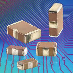
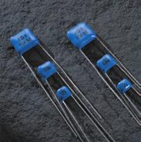
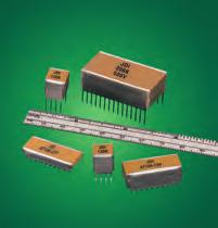
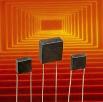
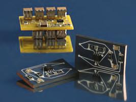
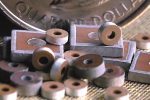
63 JOHANSON DIELECTRICS, INC. SYLMAR, CALIFORNIA X2Y EMI Filter Capacitors High Voltage Ceramic Capacitors Tanceram Ceramic Capacitors Y1 & Y2 Safety Certified Capacitors Switchmode Ceramic Capacitors Radial Leaded High Voltage MLCCs High Temperature Radial Leaded MLCCs ADVANCED MONOLYTHIC CERAMICS OLEAN, NEW YORK Ceramic Planar Array Filters Capstrate Capacitor Substrate Discodial EMI Capacitor 63

64 Your Technology Partner ANTENNA (DIVERSITY) LNA BP FILTER PA COUPLER DIPLEXER BALUN BALUN FILTER DIVIDER LTCC MODULE LP FILTER BP FILTER BALUN CHIP & WIREWOUND INDUCTORS VCO MOD. HIGH CV & LOW ESR CAPACITORS DEMOD Typical Product Applications: WiFi, WiMax, UWB, Bluetooth, Zigbee, GPS, WCDMA/GSM/GPRS & custom EUROPE: JOHANSON EUROPE, LTD. Flackwell Heath, Bucks, England HP10 9NR TEL FAX UNITED STATES: HEADQUARTERS 4001 Calle Tecate, Camarillo, California TEL (805) FAX (805) HONG KONG: JOHANSON HONG KONG, LTD. Unit E, 11/F., Phase 1 Kaiser Estate 41 Man Yue St., Hunghom Kowloon, Hong Kong TEL FAX asiasales@johansontechnology.com TAIWAN: JOHANSON HONG KONG, LTD. TAIWAN OFFICE 9F., No.403, Sec. 4, Ren-Ai Road, Da-An District Taipei, Taiwan (R.O.C.) TEL FAX asiasales@johansontechnology.com SHENZHEN: JOHANSON TRADING (SHENZHEN) CO., LTD. Room 2303, Changping Business Building, No.99 Honghua Road, Futian Free Trade Zone, Shenzhen, PRC TEL FAX asiasales@johansontechnology.com
High Frequency Ceramic Solutions
 High Frequency Ceramic Solutions RoHS Compliance 2011 Edition Antennas Baluns Capacitors - Low Loss Couplers Combiners Diplexers Filters - Notch, BP, LP Inductors IPC s (Integrated Passive Components)
High Frequency Ceramic Solutions
 RoHS/REACH Compliance High Frequency Ceramic Solutions Antennas (88 MHz-10 GHz) Baluns Capacitors (Hi Q, Low Loss) Chipset-Specific Impedance Matched Balun-Filters Couplers Diplexers Filters (Band-Pass,
RF WIREWOUND CHIP INDUCTORS
 RF WIREWOUND CHIP INDUCTORS These high frequency High-Q chip inductors feature a monolithic body made of low loss ceramic wound with wire to achieve optimal high frequency performance. These RF chip inductors
RF CERAMIC CHIP INDUCTORS
 RF CERAMIC CHIP INDUCTORS High frequency multi-layer chip inductors feature a monolithic body made of low loss ceramic and high conductivity metal electrodes to achieve optimal high frequency performance.
Power Transmitter Capacitors UHF/RF High Q Ceramic Capacitors (NP0 TC) 6040C (.600 x.400 ) 6040C (.600 x.400 )
 6040C (.600 x.400 ) 6040C (.600 x.400 )") Power Transmitter Capacirs UHF/RF High Q Ceramic Capacirs (NP0 TC) (.600 x.400 ) (.600 x.400 ) Product Features High Q, High RF Current/, High RF Power, Low ESR/ESL, Low Noise, Ultra-Stable Performance.
Power Transmitter Capacirs UHF/RF High Q Ceramic Capacirs (NP0 TC) (.600 x.400 ) (.600 x.400 ) Product Features High Q, High RF Current/, High RF Power, Low ESR/ESL, Low Noise, Ultra-Stable Performance.
RF & MICROWAVE CAPACITORS LASER TRIM CERAMIC CHIP CAPACITORS TEMEX. Multilayer ceramic Porcelain - Lasertrim. Applications.
 LASER TRIM CERAMIC CHIP CAPACITORS Applications Laser-Trim tuning capacitors are laser adjustable monolithic ceramic surface mount devices for precise functional tuning of R.F. circuits. Laser-Trim have
Buried Broadband Capacitors How To Order
 Quick Select by Application and Resonant Free Bandwidth Size Resonant Free Bandwidth** Typical Insertion Loss (S21)*** 2 Cap Values in Parallel (pf) Temp. Coeff. Working VDC FIT Calc. using cont. op. temp.
High-Q Capacitors (Microwave Chip Capacitors)
") High-Q Capacitors (Microwave Chip Capacitors) Series: ECD Features Low with tight tolerance (0. to 5.0 pf, +/ 0.05 pf to +/ 5 %) High Q value / Low ESR at High Frequencies Ultra-Stable C0G Performance
High-Q Capacitors (Microwave Chip Capacitors) Series: ECD Features Low with tight tolerance (0. to 5.0 pf, +/ 0.05 pf to +/ 5 %) High Q value / Low ESR at High Frequencies Ultra-Stable C0G Performance
WIRE WOUND CHIP INDUCTORS SWI SERIES
 S SWI SERIES INTRODUCTION The SWI series are wire wound chip inductors widely used in the communication applications such as cellular phones, cable modem, ADSL, repeaters, Bluetooth, and other electronic
WIRE WOUND CHIP INDUCTORS SWI SERIES
 S SWI SERIES INTRODUCTION The SWI series are wire wound chip inductors widely used in the communication applications such as cellular phones, cable modem, ADSL, repeaters, Bluetooth, and other electronic
WIRE WOUND CHIP INDUCTORS SWI SERIES
 S SWI SERIES INTRODUCTION The SWI series are wire wound chip inductors widely used in the communication applications such as cellular phones, cable modem, ADSL, repeaters, Bluetooth, and other electronic
AS9100 and ISO 9001 certified ISO certified
 front cover Company Overview Dielectric Laboratories, Inc. (DLI) is your global partner for application specific microwave and millimeter wave components serving customers in fiber optic, wireless, medical,
1111C/P (.110 x.110 )
") Traditional High Q (>10,000) Low ESR Capacits Product Features High Q, High Power, Low ESR/ESL, Low Noise, High Self-Resonance, Ultra-Stable Perfmance. Product Application Typical Functional Applications:
Traditional High Q (>10,000) Low ESR Capacits Product Features High Q, High Power, Low ESR/ESL, Low Noise, High Self-Resonance, Ultra-Stable Perfmance. Product Application Typical Functional Applications:
Surface Mount Multilayer Ceramic Chip Capacitors for High Frequency Applications
 Surface Mount Multilayer Ceramic Chip Capacitors for High Frequency Applications FEATURES Ultra-stable dielectric offering a Temperature Coefficient of Capacitance (TCC) of 0 ppm/ C ± 30 ppm/ C over the
DATA SHEET SURFACE-MOUNT CERAMIC MULTILAYER CAPACITORS High-voltage SC type: NP0/X7R (Pb Free & RoHS compliant)
") DATA SHEET SURFACE-MOUNT CERAMIC MULTILAYER CAPACITORS High-voltage SC type: (Pb Free & RoHS compliant) 2.2 pf to 4.7 nf Product specification Mar 1, 2007 V. 0 Product specification 2 SCOPE This specification
DATA SHEET SURFACE-MOUNT CERAMIC MULTILAYER CAPACITORS High-voltage SC type: (Pb Free & RoHS compliant) 2.2 pf to 4.7 nf Product specification Mar 1, 2007 V. 0 Product specification 2 SCOPE This specification
WIRE WOUND CHIP INDUCTORS SWI SERIES
 S SWI SERIES INTRODUCTION The SWI series are wire wound chip inductors widely used in the communication applications such as cellular phones, cable modem, ADSL, repeaters, Bluetooth, and other electronic
HIGH TEMPERATURE 150 C 180 C 200 C 230 C 250 C 350 C
 HIGH TEMPERATURE 150 C 180 C 200 C 230 C 250 C 350 C CERAMIC CAPACITORS Catalog 3500 REV. B Presidio Components has been an industry leader in the manufacture of ceramic capacitors since 1980. We are dedicated
0505C/P (.055 x.055 )
") Traditional High Q (>10,000) Low ESR Capacits Product Features High Q, High Power, Low ESR/ESL, Low Noise, High Self-Resonance, Ultra-Stable Perfmance. Product Application Typical Functional Applications:
Traditional High Q (>10,000) Low ESR Capacits Product Features High Q, High Power, Low ESR/ESL, Low Noise, High Self-Resonance, Ultra-Stable Perfmance. Product Application Typical Functional Applications:
Wire Wound Chip Inductor Low Profile Type LWL LWL1008. Features. Applications
 Wire Wound Chip Inductor Low Profile Type Wire Wound Chip Inductor Low Profile Type Features Ceramic base provides high SRF Ultra-compact inductors provide high Q factors Miniature SMD chip inductor for
ATC 100 B Series Porcelain Superchip Multilayer Capacitors
 AC 00 Series Porcelain Superchip Multilayer Capacitors Case Size Capacitance Range (" x ") 0. pf to 000 pf High Q Ultra-Stable Performance ow ESR/ES High Self-Resonance ow Noise Established Reliability
Types MC and MCN Multilayer RF Capacitors
 High-Frequency, High-Power, High-Voltage Chips with Nonmagnetic Option Rugged fexibility and compatibility with FR4 boards make Type MC and MCN capacitors ideal for use where other multilayer caps aren
ATC 800 R Series NPO Ceramic, High RF Power Lowest ESR Multilayer Capacitors
 AC 800 R Series NPO Ceramic, High RF Power owest ESR Multilayer Capacitors Case R Size (.070 x.090 ) Rugged, reliable NPO dielectric Optimized for highest self resonant frequency AC s 800 R Series offers
DATA SHEET SURFACE-MOUNT CERAMIC MULTILAYER CAPACITORS Mid-voltage: NP0/X7R (Pb Free & RoHS compliant)
") w DATA SHEET SURFACE-MOUNT CERAMIC MULTILAYER CAPACITORS Mid-voltage: NP0/X7R (Pb Free & RoHS compliant) 100 V TO 500 V 10 pf to 470 nf Product specification Sep 08, 2005 V. 0 Product specification 2 SCOPE
w DATA SHEET SURFACE-MOUNT CERAMIC MULTILAYER CAPACITORS Mid-voltage: NP0/X7R (Pb Free & RoHS compliant) 100 V TO 500 V 10 pf to 470 nf Product specification Sep 08, 2005 V. 0 Product specification 2 SCOPE
Wire Wound Chip Inductors LPI0805FT Series
 INTRODUCTION Product : LPI Miniature SMD Inductor For Power Line Size : 0805 The LPI series are low profile inductor used in notebook, PC, cellular phone backlight, inverter and etc. The devices are designed
ATC 100 B Series Porcelain Superchip Multilayer Capacitors
 AC 00 Series Porcelain Superchip Multilayer Capacitors Case Size Capacitance Range (.0" x.0") 0. pf to 000 pf High Q Ultra-Stable Performance ow ESR/ES High Self-Resonance ow Noise Established Reliability
DATA SHEET SURFACE-MOUNT CERAMIC MULTILAYER CAPACITORS High-voltage: NP0/X7R (Pb Free & RoHS compliant)
") w DATA SHEET SURFACE-MOUNT CERAMIC MULTILAYER CAPACITORS High-voltage: NP0/X7R (Pb Free & RoHS compliant) 1K V TO 4K V 10 pf to 33 nf Sep 30, 2005 V. 1 2 SCOPE This specification describes Highvoltage
w DATA SHEET SURFACE-MOUNT CERAMIC MULTILAYER CAPACITORS High-voltage: NP0/X7R (Pb Free & RoHS compliant) 1K V TO 4K V 10 pf to 33 nf Sep 30, 2005 V. 1 2 SCOPE This specification describes Highvoltage
Features. Circuit Schematic. Typical Electrical Characteristics. Applications. Surface Mount EMI Filters Three Terminal Chips. Three Terminal Chips
 Features Excellent performance in high current applications Non-polar, surface mountable Superior filtering characteristics Superb ability to withstand transient voltages and surge Offers exceptional solderability
Chip Inductor INTRODUCTION FEATURE AND APPLICATION. Feature. Application
 INTRODUCTION Multilayer Chip Inductor is an electronic part that uses in resonance circuit, for noise suppression and for impedance matching in the electrical circuit. SAMSUNG Electro-mechanics has 2 series
MICRO INDUCTORS. Features. Applications. Ordering Information. Shape and Dimensions MI - I J J T (1) (2) (3) (4) (5) (6) (7)
 (2) (3) (4) (5) (6) (7)") MICRO INDUCTORS Features 1. Very high Self-Resonant Frequencies 2. Ultra miniature size and light(0.6mm mm mm). No polarity 4. Terminal electrode has excellent solder heat resistance for soldering. 5.
MICRO INDUCTORS Features 1. Very high Self-Resonant Frequencies 2. Ultra miniature size and light(0.6mm mm mm). No polarity 4. Terminal electrode has excellent solder heat resistance for soldering. 5.
ATC 100 B Series Porcelain Superchip Multilayer Capacitors
 AC Series Porcelain Superchip Multilayer Capacitors Case Size Capacitance Range (.0 x.0 ) 0. pf to 0 pf High Q ow ESR/ES ow Noise Extended VDC up to 500 VDC Ultra-Stable Performance High Self-Resonance
WIRE WOUND CHIP INDUCTORS HCI SERIES HCI 0805 F T 1R0 K - Introductions. Features. Part Number Code HCI SERIES
 HCI SERIES WIRE WOUND CHIP INDUCTORS HCI SERIES Introductions Product : HCI Miniature SMD Inductor For Power Line Size : 0805 The HCI series are low profile inductor used in notebooks, PC s, Cellular phone
Types MCH and MCHN Multilayer High RF Power Capacitors
 2500 & 4000 Volt RF Capacitors for Medical Imaging Coils, Plasma Generators, VHF/UHF Power Amplifiers and Antenna Tuning with Nonmagnetic Option The flexible aluminum silicate dielectric eliminates cracking
AMERICAN TECHNICAL CERAMICS PRODUCT SELECTION GUIDE QUICK REFERENCE ISO 9001 REGISTERED COMPANY
 AMERICAN TECHNICAL CERAMICS QUICK REFERENCE PRODUCT SELECTION GUIDE ISO 9001 REGISTERED COMPANY QUICK REFERENCE PRODUCT SELECTION GUIDE Corporate Profile American Technical Ceramics Corp. (ATC) provides
Thin Film Current Sensing Chip Resistor (TCS Series)
") (TCS Series) Features -Thin film process -High power rating up to 3 Watts in 2512 size -Tight tolerance down to ±0.5% -Extremely low TCR down to PPM/ C -Resistance values from 50m to 1ohm -High purity
(TCS Series) Features -Thin film process -High power rating up to 3 Watts in 2512 size -Tight tolerance down to ±0.5% -Extremely low TCR down to PPM/ C -Resistance values from 50m to 1ohm -High purity
Model BD1631J50100AHF
 Model BD1631J51AHF Ultra Low Profile 85 Balun 5Ω to 1Ω Balanced Description The BD1631J51AHF is a low profile sub-miniature balanced to unbalanced transformer designed for differential inputs and output
50W TO220 High Power Resistors
 50W TO220 High Power Resistors MHP 50 Non-inductive, thin film technology. Thermally enhanced Industry standard TO220 package. RoHS compliant. Low thermal resistance, 2.3 C/W resistor hot spot to metal
Surface Mount Multilayer Ceramic Chip Capacitors DSCC Qualified Type 03028
 Surface Mount Multilayer Ceramic Chip Capacitors DSCC Qualified Type 03028 FEATURES US defense supply center approved Federal stock control number, Available CAGE CODE 2770A Available Small case size (0603)
Sunlord Wire Wound SMD Power Inductor Page 1 of 7 SPECIFICATIONS
 Sunlord Wire Wound SMD Power Inductor Page 1 of 7 SPECIFICATIONS Customer Product Name Wire Wound SMD Power Inductor Sunlord Part Number SWPA4020S T Customer Part Number [ New Released, Revised] SPEC No.:
Chip Resistors / Chip Arrays
 Chip Resistors / Chip Arrays w w w. b o u r n s. c o m I. CR Series Chip Resistors...92 II. CAT/CAY Series Chip Resistor Arrays...96 CAT/CAY 16 Series...96 CAY1 Chip Resistor Array...97 CAY17 Bussed Resistor
(TRMA) Multilayer Ferrite Beads Chip Inductors. Token Electronics Industry Co., Ltd. Version: January 13, Web:
 Multilayer Ferrite Beads Chip Inductors. Token Electronics Industry Co., Ltd. Version: January 13, Web:") Version: January 13, 2017 (TRMA) Multilayer Ferrite Beads Chip Inductors Token Electronics Industry Co., Ltd. Web: www.token.com.tw Email: rfq@token.com.tw Taiwan: No.137, Sec. 1, Zhongxing Rd., Wugu District,
Version: January 13, 2017 (TRMA) Multilayer Ferrite Beads Chip Inductors Token Electronics Industry Co., Ltd. Web: www.token.com.tw Email: rfq@token.com.tw Taiwan: No.137, Sec. 1, Zhongxing Rd., Wugu District,
ATC 100 B Series Porcelain Superchip Multilayer Capacitors
 AC Series Porcelain Superchip Multilayer Capacitors Case Size Capacitance Range (" x ") 0. pf to 0 pf High Q Ultra-Stable Performance ow ESR/ES High Self-Resonance ow Noise Established Reliability (QP)
ATC 200 B Series BX Ceramic Multilayer Capacitors
 AC 200 Series X Ceramic Multilayer Capacitors Case Size Capacitance Range (.110" x.110") 5000 pf to 0.1 µf ow ESR/ES Mid-K Rugged Construction High Reliability Extended VDC Available AC, the industry leader,
ATC 100 B Series Porcelain Superchip Multilayer Capacitors
 AC Series Porcelain Superchip Multilayer Capacitors Case Size Capacitance Range (.0" x.0") 0. pf to 0 pf High Q Ultra-Stable Performance ow ESR/ES High Self-Resonance ow Noise Established Reliability (QP)
CR0603/CR0805/CR Chip Resistors
 *RoHS COMPLIANT Features RoHS compliant* Power rating at 7 C: CR63 -.1 W, CR85 -.125 W, CR126 -.25 W Tight tolerances of bottom electrode width Suitable for all types of soldering processes Three layer
ATC 100 B Series Porcelain Superchip Multilayer Capacitors
 AC Series Porcelain Superchip Multilayer Capacitors Case Size Capacitance Range (." x.") 0. pf to 0 pf High Q Ultra-Stable Performance ow ESR/ES High Self-Resonance ow Noise Established Reliability (QP)
YAGEO CORPORATION SMD INDUCTOR / BEADS. Notebook computers, step-up and step-down converters. Flash memory programmers, etc...
 YAGEO CORPORATION SMD INDUCTOR / BEADS SMD Power Inductors SDS0402 Series These shielded ultra-miniature inductors can help designers achieving significantly longer battery life in handheld communication
Wire Wound Chip Inductor
 Features Ceramic base provide high Ultra-compact inductors provide high Q factors ow profile, high current options Miniature SMD chip inductor for fully automated assembly Outstanding endurance from Pull-up
Thin Film Precision Chip Resistor (AR Series)
") Features Advanced thin film technology Very tight tolerance down to ±0.01% Extremely low down to ±5PPM/C Wide resistance range 1ohm ~ 3Mega ohm Miniature size 0201 available Thin Film Precision Chip Resistor
Features Advanced thin film technology Very tight tolerance down to ±0.01% Extremely low down to ±5PPM/C Wide resistance range 1ohm ~ 3Mega ohm Miniature size 0201 available Thin Film Precision Chip Resistor
(TREC) Wire Wound RF Chip Inductor
 Wire Wound RF Chip Inductor") Version: February 21, 2017 (TREC) Wire Wound RF Chip Inductor Token Electronics Industry Co., Ltd. Web: www.token.com.tw Email: rfq@token.com.tw Taiwan: No.137, Sec. 1, Zhongxing Rd., Wugu District, New
Version: February 21, 2017 (TREC) Wire Wound RF Chip Inductor Token Electronics Industry Co., Ltd. Web: www.token.com.tw Email: rfq@token.com.tw Taiwan: No.137, Sec. 1, Zhongxing Rd., Wugu District, New
 Distributed by: www.jameco.com 1-8-831-4242 The content and copyrights of the attached material are the property of its owner. *RoHS COMPLIANT VERSIONS AVAILABLE Features Lead free version available (see
(TREM) High SRFs RF Inductor
 High SRFs RF Inductor") Version: March 1, 2017 Electronics Tech. (TREM) High SRFs RF Inductor Web: www.direct-token.com Email: rfq@direct-token.com Direct Electronics Industry Co., Ltd. China: 12F, Zhong Xing Industry Bld., Chuang
Version: March 1, 2017 Electronics Tech. (TREM) High SRFs RF Inductor Web: www.direct-token.com Email: rfq@direct-token.com Direct Electronics Industry Co., Ltd. China: 12F, Zhong Xing Industry Bld., Chuang
Model B0922N7575AHF Rev B. Ultra Low Profile 0404 Balun
 Model B9N7575AHF Ultra Low Profile 44 Balun 75Ω to 75Ω Balanced Description The B9N7575AHF is a low profile, low impedance mm square subminiature wideband unbalanced to balanced transformer designed for
X2Y for Today s Circuits
 X2Y for Today s Circuits Circuit designers today are challenged with maintaining Signal and Power Integrity amid increasing Electro-Magnetic Compliance (EMC) requirements, while at the same time lowering
DATA SHEET SURFACE-MOUNT CERAMIC MULTILAYER CAPACITORS Ultra small: NP0/X5R/X7R/Y5V (Pb Free & RoHS compliant)
") DATA SHEET SURFACE-MOUNT CERAMIC MULTILAYER CAPACITORS : NP0/X5R/X7R/Y5V (Pb Free & RoHS compliant) 6.3 V TO 50 V 1 pf to 100 nf Product specification Product specification 2 Surface-Mount Ceramic Multilayer
DATA SHEET SURFACE-MOUNT CERAMIC MULTILAYER CAPACITORS : NP0/X5R/X7R/Y5V (Pb Free & RoHS compliant) 6.3 V TO 50 V 1 pf to 100 nf Product specification Product specification 2 Surface-Mount Ceramic Multilayer
ATC 800 E Series NPO Ceramic High RF Power Multilayer Capacitors
 AC 800 Series NPO Ceramic High RF Power Multilayer Capacitors Case Size Capacitance Range: (" x ") 3.3 pf to 500 pf High Q Ultra-Stable Performance Ultra ow SR High RF Current/Voltage High RF Power High
CHQ SERIES. Surface Mount Chip Capacitors: Ultra High Frequency
 26 High Frequency Measurement and Performance of High Multilayer Ceramic Capacitors Introduction Capacitors used in High Frequency applications are generally used in two particular circuit applications:
IWHQSeries FEATURES ORDERING CODE. SMD Wirewound Open-Type Chip Inductors (High Q /Frequency) 0805 TRIGON COMPONENTS
 0805 TRIGON COMPONENTS") CONFIGURATIONS: FEATURES Low DC resistance design is ideal for low loss, high output and low power consumption. Especially high Q factor in this series for customer s design. Resin-coated surface enables
CONFIGURATIONS: FEATURES Low DC resistance design is ideal for low loss, high output and low power consumption. Especially high Q factor in this series for customer s design. Resin-coated surface enables
P21BN300M5S Milli Cap
 P21BN300M5S Milli Cap Milli Cap : The "Ideal" SMT Capacitor Benefits: Increased Useable Bandwidth Very Low Series Inductance Ultra High Series Resonance Low Loss, High Q Functional Applications: Matching
RF and MICROWAVE DISCRETE LOW POWER TRANSISTORS Qualified per MIL-PRF-19500/343
 Available on commercial versions RF and MICROWAVE DISCRETE LOW POWER TRANSISTORS Qualified per MIL-PRF-19500/343 DESCRIPTION The 2N2857UB is a military qualified silicon NPN transistor (also available
Migrating 4195A to E5061B LF-RF Network Analyzer. April 2010 Agilent Technologies
 Migrating 4195A to E61B LF-RF Network Analyzer April 2010 Agilent Technologies Page 1 Contents Overview of 4195A to E61B migration Migrating 4195A to E61B in network measurements Migrating 4195A to E61B
Model C2327J5003AHF Rev D
 Model C2327J53AHF Ultra Low Profile 85 3 db, 9 Hybrid Coupler Description The C2327J53AHF is a low cost, low profile sub-miniature high performance 3 db coupler in an easy to use surface mount package.
Detailed Electrical Specifications: Specifications subject to change without notice. Broadband Narrowband 25 C
 fee Ultra Low Profile 85 Balun 75Ω to 75Ω Balanced Description The B225J7575AHF is a low profile sub-miniature balanced to unbalanced transformer designed for differential inputs and output locations on
Model C0810J5003AHF. Ultra Low Profile db, 90 Hybrid Coupler
 Model C81J53AHF Ultra Low Profile 85 3 db, 9 Hybrid Coupler Description The C81J53AHF is a low cost, low profile sub-miniature high performance 3 db coupler in an easy to use surface mount package. It
High Frequency Ceramic Solutions
 Date: 06/04/2014 2.1mm Abstract The nrf51822 and nrf51422 devices from Nordic Semiconductor are powerful, highly flexible, multiprotocol SoCs designed for Bluetooth low energy, ANT, and 2.4 GHz ultralow
Model BD1722J50100A00
 Ultra Low Profile 85 Balun 5Ω to 1Ω Balanced Description The BD1722J51A is a low profile sub-miniature balanced to unbalanced transformer designed for differential inputs and output locations on next generation
ICL Series SMD Wirewound Chip Open-Type Inductors - ICL0603, ICL0805
 SMD Wirewound Chip Open-Type s - ICL0603, ICL0805 CONFIGURATIONS: FEATURES Lower profile,high frequency Higher possible SRFs as well as excellent Q Value Higher current in compact size Customer design
SMD High Frequency Power Inductor. Designed for VRD & VRM 10.x & 11.x Applications
 Designed for VRD & VRM 1.x & 11.x Applications FEATURES Recommended for use with all major Voltage Regulator ICs High Current handling capability in the smallest footprint Up to 2MHz operating frequency
Shortform Official Distributors for Australia and New Zealand. Fairmont MARKETING. fairmontmarketing.com.au TOTAL SOLUTIONS. dlpc.com.
 Shortform 2019 Official Distributors for Australia and New Zealand Fairmont 1 High Voltage MLCC Capacitors Space Saving, High Quality Johanson Dielectrics high voltage MLCC capacitors feature a special
DATASHEET CUSTOMER : 승인번호 ISSUE DATA SHEET. We have approved the attached specification. Written by Checked by Approved by
 CUSTOMER : 승인번호 ISSUE DATA SHEET Product Name : Part No : Revision Date : 2012/11/23 Customer Code : We have approved the attached specification. Written by Checked by Approved by CUSTOMER Signature R
Monolithic Amplifier CMA-103+ Ultra Linear Low Noise, Ceramic to 4 GHz
 Ultra Linear Low Noise, Ceramic Monolithic Amplifier 50Ω 0.05 to 4 GHz The Big Deal Ceramic, hermetically sealed, nitrogen filled Low profile case, 0.045 Ultra High IP3 Broadband High Dynamic Range CASE
Model BD4859L50100A00 Rev A
 Model BD4859L51A Ultra Small Low Profile 63 Balun 5Ω to 1Ω Balanced Description The BD4859L51A is an ultra-small low profile balanced to unbalanced transformer designed for differential inputs and output
Surface Mount EMI Filters
 Surface Mount EMI Filters our family of surface mount filters is designed to provide a range of high performance EMI filtering options with a minimal PCB footprint Three Terminal Chips offer superior ability
Model PD3150J5050S2HF
 Model PD315J55S2HF Ultra Low Profile 85 Power Divider 5Ω to 5Ω Description The PD315J55S2HF is a low profile, sub-miniature Wilkinson power divider in an easy to use surface mount package. The PD315J55S2HF
Model PD2328J5050S2HF
 Model PD2328J55S2HF Ultra Low Profile 85 Power Divider 5Ω to 5Ω Description The PD2328J55S2HF is a low profile, sub-miniature Wilkinson power divider in an easy to use surface mount package. The PD2328J55S2HF
Power Inductors, Shielded
 The Shielded Power are low profile, surface-mount inductors. They are designed for power applications or high current applications. Key Features High reliability and easy surface mount assembly Low loss
MTE1 Series Isolated 1W Single Output SM DC/DC Converters
 MTE1 Series SELECTION GUIDE FEATURES Single isolated output 1kVDC Isolation Typical efficiency 86% Wide temperature performance at full 1 Watt load, 4 C to 85 C UL 94V- Package material 3.3V, 5V, 12V,
Model BD3238N5050AHF. Ultra Low Profile 0404 Balun
 Model BD338N55AHF Ultra Low Profile 44 Balun 5Ω to 5Ω Balanced Description The BD338N55AHF is a low cost, low profile sub-miniature unbalanced to balanced transformer designed for differential inputs and
VT-841 VT-841. Temperature Compensated Crystal Oscillator. Description. Applications. Features. Block Diagram. Output V DD.
 VT-841 Temperature Compensated Crystal Oscillator VT-841 Description Vectron s VT-841 Temperature Compensated Crystal Oscillator (TCXO) is a quartz stabilized, clipped sine wave output, analog temperature
Model 2425B50-50C Rev. A
 rit Model 2425B50-50C Xinger Balun 50Ω to 100Ω Balanced Description The 2425B50-50C is a low profile sub-miniature balanced to unbalanced transformer designed for differential inputs and output locations
Multilayer Ferrite Chip Inductor
 FEATURES Skywell multiplayer chip inductor is formed without a wound wire and has a closed magnetic circuit formed by simultaneous forming of alternative layers of ferrite paste and conductor paste. High
10 nh Inductor (Top View)
") SMD High- RF Inductor nh Inductor (Top View) ACCU- TECHNOOGY The SMD Inductor is based on thin-film mul ti lay er technology. This technology provides a level of control on the elec tri cal and physical
SMD High- RF Inductor nh Inductor (Top View) ACCU- TECHNOOGY The SMD Inductor is based on thin-film mul ti lay er technology. This technology provides a level of control on the elec tri cal and physical
CERAMIC MICROWAVE FILTERS SAW FILTERS. SAF Series
 SAW S FEATURES Standard part frequency range (80MHz 2.0GHz) Low passband ripple Linear phase High selectivity APPLICATIONS Cellular Phone: E-AMPS, PCS and GSM, PDC Cordless Phone: CT-1, ISM, DECT Land
Thin Film Precision Chip Resistor (AR Series)
") Construction D1 L (AR Series) Features -Advanced thin film technology -Very tight tolerance down to ±0.01% -Extremely low TCR down to PPM/ C -Wide resistance range 1ohm ~ 3Mega ohm -Miniature size 0201
Construction D1 L (AR Series) Features -Advanced thin film technology -Very tight tolerance down to ±0.01% -Extremely low TCR down to PPM/ C -Wide resistance range 1ohm ~ 3Mega ohm -Miniature size 0201
C 062 C 105 K 1 R 5 T A Rated Voltage (VDC) 5 = 50 1 = = 200
 5 = 50 1 = = 200") Radial Through Hole Multilayer Ceramic Capacitors Radial, Molded, X7R Dielectric, 50 200 VDC (Commercial Grade) Overview KEMET s epoxy molded radial through-hole ceramic capacitors in X7R dielectric feature
Radial Through Hole Multilayer Ceramic Capacitors Radial, Molded, X7R Dielectric, 50 200 VDC (Commercial Grade) Overview KEMET s epoxy molded radial through-hole ceramic capacitors in X7R dielectric feature
"High Frequency Ceramic Solutions"
 Page 1 of 12 AEC-Q200 qualification available. General Specifications Part Number Frequency (MHz Peak Gain (dbi typ. Impedance Input Power 3 min. 1 Measured on a 30x40mm GND plane. Eval Board p/n 0900AD47A2450-EB1SMA
RF Inductor Series. Electronics Tech. Direct Electronics Industry Co., Ltd. Version: July 23, 2018
 Version: July 23, 2018 Electronics Tech. RF Inductor Series Web: www.direct-token.com Email: rfq@direct-token.com Direct Electronics Industry Co., Ltd. China: 12F, Zhong Xing Industry Bld., Chuang Ye Road,
Typical Performance Data
 Ceramic Balun RF Transformer 50Ω 720 to 1600 MHz Maximum Ratings Operating Temperature -40 C to 85 C Storage Temperature -55 C to 100 C Input RF Power*** 3W **Derate linearly to 2.5W at 100 C Permanent
SMD High Frequency Power Inductor. Designed for Utility Regulator Applications
 FEATURES Recommended for use with all major Voltage Regulator ICs High Current handling capability in the smallest footprint Up to 2MHz operating frequency Extended operating temperature range: -4C to
S C A 69 B 104 J W S. Capacitance Code (pf)
") SCA Series, Axial, C 3 Technology, C0G Dielectric, 50 200 VDC (Commercial Grade) Overview KEMET s SCA Series axial through-hole ceramic capacitors in C0G dielectric feature proprietary Ceramic Cased Capacitor
SCA Series, Axial, C 3 Technology, C0G Dielectric, 50 200 VDC (Commercial Grade) Overview KEMET s SCA Series axial through-hole ceramic capacitors in C0G dielectric feature proprietary Ceramic Cased Capacitor
"High Frequency Ceramic Solutions"
 2.45 GHz High Gain Chip Antenna ( Orientation P/N 2450AT45A100 Detail Specification: 01/05/2012 Page 1 of 10 General Specifications Part Number Frequency Range Peak Gain Average Gain 2450AT45A100 2400-2500
(TRMB) Multilayer Bead RF Inductors. Token Electronics Industry Co., Ltd. Version: January 13, Web:
 Multilayer Bead RF Inductors. Token Electronics Industry Co., Ltd. Version: January 13, Web:") Version: January 13, 2017 (TRMB) Multilayer Bead RF Inductors Token Electronics Industry Co., Ltd. Web: www.token.com.tw Email: rfq@token.com.tw Taiwan: No.137, Sec. 1, Zhongxing Rd., Wugu District, New
Version: January 13, 2017 (TRMB) Multilayer Bead RF Inductors Token Electronics Industry Co., Ltd. Web: www.token.com.tw Email: rfq@token.com.tw Taiwan: No.137, Sec. 1, Zhongxing Rd., Wugu District, New
Model BD2425N50200AHF. Ultra Low Profile 0404 Balun 50Ω to 200Ω Balanced
 Model BD45N5AHF Ultra Low Profile 44 Balun 5Ω to Ω Balanced Description The BD45N5AHF is a low cost, low profile sub-miniature unbalanced to balanced transformer designed for differential inputs and output
Glass Encapsulated SMD Varistor MLV
 (VJ12, 2, 13, 14, 15, 32) Transient Voltage Suppression, ESD Protection Devices & EMI Devices GENERAL DESCRIPTION AVX s Professional Multilayer Varistors include 3 series of glass coated products as listed
Return loss (db) Insertion loss (db) .56±.06 TBD. GND / DC Feed 1 + RF GND 2. Unbalanced Port Balanced Port Balanced Port.
 Insertion loss (db) .56±.06 TBD. GND / DC Feed 1 + RF GND 2. Unbalanced Port Balanced Port Balanced Port.") Model BD6N5AHF Ultra Low Profile 44 Balun 5Ω to Ω Balanced Description The BD6N5AHF is a low cost, low profile sub-miniature unbalanced to balanced transformer designed for differential inputs and output
Model BD6N5AHF Ultra Low Profile 44 Balun 5Ω to Ω Balanced Description The BD6N5AHF is a low cost, low profile sub-miniature unbalanced to balanced transformer designed for differential inputs and output
INPAQ. Specification. WIP201610S L Series. Product Name. Power Inductor. Global RF/Component Solutions
 WIP201610S L Series Specification Product Name Series Power Inductor WIP201610S L Series Size EIAJ 2016 WIP201610S L Series Engineering Specification 1. Scope Feature High saturation current realized by
Kete Microwave Electronics Co., Ltd.
 HOW TO ORDER: KTFC - X XX X - XX XX - XXX XX - XXXX - XXXX Large Dia. Body Width Rated Voltage Kete Small Dia Lead Dia. VDC/VAC Feedthru Capacitors Dielectric X=X7R, S=SL, N=NPO (-55 ~+125 ) Y=Y5U, Y5V
AMCA R450G-S1F-T3 Pb
 FEATURES APPLICATIONS 2450MHz, bandwidth 90MHz Small size - 3.2 x 1.6 x 1.2mm (0.125 x 0.62 x 0.047 inch) Gain 0.5dBi (Peak) / -1dBi (Average) VSWR
ATC 100 C Series Porcelain High RF Power Multilayer Capacitors
 A 100 Series Porcelain High RF Power Multilayer apacitors ase Size apacitance Range (.250" x.250") 1 pf to 2700 pf High Q Ultra-Stable Performance ow ESR/ES High RF urrent/voltage High RF Power High Reliability
Multilayer Ceramic Chip Capacitors
 NMC-T Low rofile Series FEATURES X7R, X5R AND Y5V DIELECTRICS HIGH CAACITANCE & LO ROFILE RoHS COMLIANT SAC SOLDER COMATIBLE RoHS Compliant Includes all homogeneous materials *See art Number System for
Type CPF Series. Thin Film Precision Resistors. Key Features
 Type CPF Series Key Features Thin film precision resistors with TC's to 15ppm and tolerances to 0.05%. Wide range of case sizes from 0201 to 2512 Suitable for all applications where close accuracy and