Implantation-Free 4H-SiC Bipolar Junction Transistors with Double Base Epi-layers
|
|
|
- Iris Hawkins
- 5 years ago
- Views:
Transcription
1 Implantation-Free 4H-SiC Bipolar Junction Transistors with Double Base Epi-layers Jianhui Zhang, member, IEEE, Xueqing, Li, Petre Alexandrov, member, IEEE, Terry Burke, member, IEEE, and Jian H. Zhao, Senior Member, IEEE, Abstract This paper reports the first 4H-SiC power bipolar junction transistor (BJT) which is completely free of ion implantation and hence is free of the implantationinduced crystal damages and high-temperature activation annealing-induced surface roughness. The BJT is designed to have double epitaxial p-type base layers with the top layer more heavily doped for direct Ohmic contact formation while at the same time supporting a robust single-step junction termination extension without the need of ion implantation. The double layers create a built-in electric field in the base region which helps to speed up injected electrons across the base and leads to an improve BJT current gain. Based on this novel design and implantation-free process, a 4H-SiC BJT has been fabricated to reach an open base collector-to-emitter blocking voltage of over 1300 V with a current gain up to 31, using a drift layer of 11.5 μm, lightly-doped to cm - 3. Index Terms Silicon carbide, bipolar junction transistors (BJTs), power transistors Jianhui Zhang, Xueqing Li and Petre Alexandrov are with United Silicon Carbide, Inc, New Brunswick Technology Center, New Brunswick, NJ 08901, USA. Terry Burke is with U.S. Army TARDEC, Warren, MI Jian H. Zhao is with SiCLAB, ECE Department, Rutgers University, Piscataway, NJ 08854, USA. 1
2 Report Documentation Page Form Approved OMB No Public reporting burden for the collection of information is estimated to average 1 hour per response, including the time for reviewing instructions, searching existing data sources, gathering and maintaining the data needed, and completing and reviewing the collection of information. Send comments regarding this burden estimate or any other aspect of this collection of information, including suggestions for reducing this burden, to Washington Headquarters Services, Directorate for Information Operations and Reports, 1215 Jefferson Davis Highway, Suite 1204, Arlington VA Respondents should be aware that notwithstanding any other provision of law, no person shall be subject to a penalty for failing to comply with a collection of information if it does not display a currently valid OMB control number. 1. REPORT DATE 14 MAY REPORT TYPE N/A 3. DATES COVERED - 4. TITLE AND SUBTITLE Implantation-Free 4H-SiC Bipolar Junction Transistors with Double Base Epi-layers 6. AUTHOR(S) Jianhui Zhang; Xueqing Li; Petre Alexandrov; Terry Burke; Jian H. Zhao 7. PERFORMING ORGANIZATION NAME(S) AND ADDRESS(ES) US Army RDECOM-TARDEC 6501 E 11 Mile Rd Warren, MI a. CONTRACT NUMBER 5b. GRANT NUMBER 5c. PROGRAM ELEMENT NUMBER 5d. PROJECT NUMBER 5e. TASK NUMBER 5f. WORK UNIT NUMBER 8. PERFORMING ORGANIZATION REPORT NUMBER 17113RC 9. SPONSORING/MONITORING AGENCY NAME(S) AND ADDRESS(ES) 10. SPONSOR/MONITOR S ACRONYM(S) TACOM/TARDEC 12. DISTRIBUTION/AVAILABILITY STATEMENT Approved for public release, distribution unlimited 13. SUPPLEMENTARY NOTES The original document contains color images. 14. ABSTRACT 15. SUBJECT TERMS 11. SPONSOR/MONITOR S REPORT NUMBER(S) 17113RC 16. SECURITY CLASSIFICATION OF: 17. LIMITATION OF ABSTRACT SAR a. REPORT unclassified b. ABSTRACT unclassified c. THIS PAGE unclassified 18. NUMBER OF PAGES 14 19a. NAME OF RESPONSIBLE PERSON Standard Form 298 (Rev. 8-98) Prescribed by ANSI Std Z39-18
3 I. INTRODUCTION 4H-SiC bipolar junction transistor (BJT) is an important switching device for high power and high temperature applications. It is an intrinsically normally-off device, does not have gate oxide problems as in SiC MOSFET and IGBT, and conducts high current with a low forward voltage drop. For 4H-SiC BJTs, high current gain is desirable in practical applications for simple control circuit design and better energy efficiency. Many studies have been reported to further increase the current gain of 4H-SiC BJTs by optimizing the emitter/base geometry [1], surface passivation [2], ion implantation [3], as well as employing continuous growth of the base and emitter epi-layers in the same reactor [1,4-6]. In the fabrication of 4H-SiC BJTs, the base Ohmic contact is usually formed on a heavily implanted p+ region. The p+ implantation also requires an activation annealing at high temperature, normally over 1500 o C. This base ion implantation process introduces crystalline damages both inside the base region and on the surface of SiC, resulting in an increased base recombination current and lowering the current gain. Our earlier experimental study showed that lower base implantation energy and dose resulted in higher current gain 4H-SiC BJTs [2]. We also reported that BJTs with unintentionally graded base doping tend to have higher current gains [7] because the built-in electric field resulting from the graded base epi-layer helps the injected electrons from the emitter to move quickly through the base, reducing the base recombination. This paper reports our first experimental effort with BJTs intentionally designed with a non-uniform base doping that will have the desired built-in electric field in the base region while making it possible to form p-type Ohmic contact to the base without ion implantation. 2
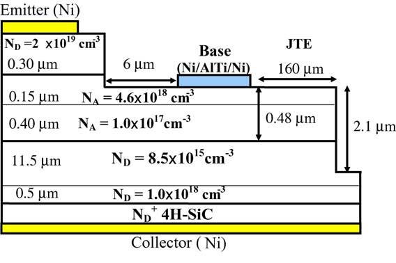
4 II. DEVICE DESIGN AND FABRICATION Fig. 1 shows a cross-sectional view of the fabricated 4H-SiC BJTs. The wafer is purchased commercially per our design. The base and emitter epi-layers are grown in separate reactors, similar to those BJTs reported before [8-10]. The emitter n + epi-layer is 0.3 μm thick, and is doped to cm -3. The base epi-layer consists of a 0.40 μm, cm -3 lightly doped epi-layer capped by a 0.15 μm, cm -3 heavily doped top epi-layer. The drift layer is 11.5 μm thick and lightly-doped to cm -3 grown on n-type buffer layer of 0.5 μm, doped to cm -3 on a heavily doped n-type 4H- SiC substrate. The fabrication process starts with a dry etching of the emitter fingers by inductively coupled plasma (ICP) in a gas mixture of freon and oxygen at an etching rate of nm/min. The p-type epi-layer was exposed in the base trench and the junction termination extension (JTE) region. A single step JTE with a width of 160 μm, based on the remaining 0.48 μm p-type base epi-layer, is formed for the edge termination. The isolation between each device is created by a mesa etching of ~1.6 μm into the drift layer. The sample is oxidized by a wet thermal oxidation for 2 hours at 1100 o C followed by a 1- hour Ar annealing at 1100 o C and a re-annealed in wet-oxygen for 3 hours at 950 o C. After the thermal oxidation, 380 nm SiO 2 and 250 nm Si 3 N 4 are deposited by PECVD to seal the thermal passivation layer. Base Ohmic contact is directly formed on the p-type epi-layer, with a designed spacing between the base contact region and the emitter mesa edge (BE-spacing) of 6 μm. Base contact metals are based on sputtered AlTi and Ni while emitter and collector Ohmic contacts are both based on sputtered Ni. The Ohmic 3
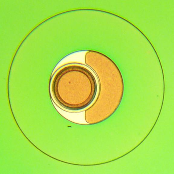
5 contact annealing is carried out at 1000 o C for 5 minutes in Argon forming gas (5% H 2 in Ar) by using a rapid thermal processing (RTP) system. After Ohmic contact formation, a thick layer of AlTi/Al/AlTi is sputtered on the base and emitter fingers to improve the voltage and current distribution along the fingers. Then, SiO 2 and Si 3 N 4 multi-layers are deposited by PECVD as the insulator between the overlay metals. The base and emitter contact windows are opened by ICP. Sputtered Ti / Au are used to form the base and emitter bonding pads as well as the collector overlay metal on the substrate. Fig. 2 shows a top-view photo of a fabricated small area 4H-SiC BJT. It has an eccentric circular geometry. The device outer diameter is 600 um. The emitter mesa is 18 μm wide, and forms an emitter mesa ring in the inner circle. The base contact region also forms a ring outside of the emitter mesa ring with a width of 10 μm. The emitter bonding pad is inside the circle formed by the emitter mesa with dielectrics insulated from the p- type 4H-SiC surface. The base bonding pad is formed at one side of the emitter, sitting directly on dielectrics. III. EXPERIMENTAL RESULTS AND DISCUSSIONS Measured from the on-chip TLM (transmission line model) structure, the emitter n-type specific contact resistance and n + emitter layer sheet resistance are Ω cm 2 and 228 Ω, respectively, while the p-type specific contact resistance and p-base sheet resistance are Ω cm 2 and 87 kω, respectively, as shown in Fig. 3. The base specific contact resistance is close to the value obtained from the implanted samples, showing that the doping concentration of 4.6x10 18 cm -3 can provide a reasonable p-type 4
6 Ohmic contact. The sheet resistance of the p-type base layer is larger by a factor of 2, compared to our previously implanted BJT samples, most like due to the smaller thickness of the base layer and the lower doping of the remaining base of the BJT design. Fig. 4 shows the common emitter I-V characteristics of a fabricated circular small area 4H-SiC BJT as shown in Fig. 3. It conducts 93.5 ma collector current when the base current is 3.0 ma, corresponding to a very good DC current gain of The open emitter blocking voltage (V CBO ) is up to 1810 V, and its open base blocking voltage (V CEO ) is 1336 V. Fig. 5 shows the common emitter I-V characteristics of a large area 4H-SiC BJT fabricated on the same double base epi-layer wafer. It has a footprint of 2.5 mm x 3.0 mm, and an active area of 4.2 mm 2 excluding the bonding pads and the JTE field region. This large area 4H-SiC BJT has an emitter mesa width of 14 um and the same BE-spacing of 6 um. It also shows a good DC current gain of 23.6 and blocks over 1130 V with a specific on-resistance of 11.2 mω.cm 2. The experimental results obtained from the double base epi-layer 4H-SiC BJTs show a high current gain, although the emitter injection efficiency may be lower in comparison to BJTs with lower base doping. This high current gain is achieved because the double base epilayer creates a built-in electric field in the base region and eliminates the need for ion implantation and high-temperature activation annealing, both leading to reduced base and surface recombination. The advantage of eliminating ion implantation lies not only in the elimination of implantation-induced crystal damages but also in the substantially simplified BJT fabrication process because many fabrication steps are eliminated, 5
7 including the critical steps of photolithography for creating ion implantation mask, shipping out samples for ion implantation, and high-temperature activation annealing. Work is on-going to design further improved BJT structure with a graded base doping that can be epitaxially grown continuously with the n+ emitter cap to maximize the builtin electric field in the base region and the BJT gain. IV. SUMMARY The first high voltage 4H-SiC BJT with double base epi-layers which are free of ion implantations and high temperature activation annealing have been successfully demonstrated. Because of the built-in electric field in the base and the elimination of implantation-induced damage and high-temperature annealing-induced surface roughness, a high current gain of 31.2 has been achieved for a BJT with an open base blocking voltage over 1.3 kv. Optimized design with gradually graded base doping and continously grown base-emitter junction, once developed, can be expected to further improve the current gain and substantially simplify the BJT fabrication by elimination many time consuming fabrication steps. Acknowledgment: Work at USCI was supported in part by a TARDEC SBIR program (DAAE07-02-C-L050). JHZ acknowledges financial support provided by United Silicon Carbide, Inc. 6
8 Fig. 1 7
9 Fig. 2 8
10 Rs=86.7 kω ρ c =6.3x10⁻³ Ω.cm R (kω) A=3125 B=578 R= Gap (μm) Fig. 3 9
11 Ic (ma) β=31.2 I B = 3 ma I B = 2 ma V CBO 1810 V 0.5 ma I B = 1 ma X100 V CEO 1336 V 0.23 ma Vce (V) Fig. 4 10
12 Ic (A) R 28 SP-ON =11.2 mω.cm 2 Active area = 4.2 mm β= I 22 B =1.0 A I 18 B =0.8 A V CBO V ma 14 I 333 B =0.6 A 12 V CEO I B =0.4 A 1130V ma I 4 X 10 4 B =0.2 A Vce (V) Jc (A/cm 2 ) Fig. 5 11
13 FIGURE CAPTIONS Fig. 1. Cross sectional view of the 4H-SiC BJT device Fig. 2. Top view photo of a fabricated small area 4H-SiC BJT. Fig. 3. TLM measurement results of the base Ohmic contact. Fig. 4. I-V characteristics of a small area 4H-SiC BJT. Fig. 5. I-V characteristics of a large area 4H-SiC BJT. 12
14 References: [1] M. Domeij, H.-S. Lee, E. Danielsson, C.-M. Zetterling, M. Ostling, and A. Schoner, Geometrical effects in high current gain 1100-V 4H-SiC BJTs, IEEE Electron Device Letters, vol. 26, pp , [2] Jianhui Zhang, Yanbin Luo, Petre Alexandrov, Leonid Fursin, and Jian H. Zhao, A high current gain 4H-SiC NPN power bipolar junction transistor, IEEE Electron Device Letters, vol. 24, pp , May [3] C.-F. Huang and J. A. Cooper, Jr., High current gain 4H-SiC NPN Bipolar Junction Transistors, IEEE Electron Device Letters, vol. 24, pp , Jun [4] Sumi Krishnaswami, Anant Agarwal, Sei-Hyung Ryu, Craig Capell, James Richmond, John Palmour, Santosh Balachandran, T. Paul Chow, Stephen Bayne, Bruce Geil, Kenneth Jones and Charles Scozzie, 1000-V, 30-A 4H-SiC BJTs with high current gain, IEEE Electron Device Letters, vol. 26, pp , Mar [5] Anant K. Agarwal, Sumi Krishnaswami, James Richmond, Craig Capell, Sei-Hyung Ryu, John W. Palmour, Santosh Balachandran, T. Paul Chow, Stephen Bayne, Bruce Geil, Charles Scozzie and Kenneth A. Jones, Evolution of the 1600 V, 20 A, SiC bipolar junction transistors, in Proc. of 17 th international symposium on power semiconductor devices & IC s (ISPSD), pp , [6] Jianhui Zhang, Petre Alexandrov, Terry Burke, and Jian H. Zhao, 4H-SiC power bipolar junction transistor with a very low specific on-resistance of 2.9 mω cm 2, IEEE Electron Device Letters, vol. 27, pp ,
15 [7] J.H. Zhao, J. Zhang, X. Li, and K. Sheng, Effect of graded base doping on the gain of SiC BJT, International Semiconductor Device Research Symposium (ISDRS), IEEE conference proceeding, pp , [8] J. Zhang, P. Alexandrov, and J. H. Zhao, High Power (500 V-70 A) and High Gain (44-47) 4H-SiC Bipolar Junction Transistors, in Materials Science Forum, vol , pp , [9] Jianhui Zhang, Petre Alexandrov, Jian H. Zhao and Terry Burke, 1677 V, 5.7 mω.cm 2 4H-SiC BJTs, IEEE Electron Device Letters, vol. 26, pp , [10] Jianhui Zhang, Jian Wu, Petre Alexandrov, Terry Burke, Kuang Sheng and Jian H. Zhao, 1836 V, 4.7 mω.cm 2 high power 4H-SiC bipolar junction transistor, Materials Science Forum, vol , pp ,
4H-SiC Power Bipolar Junction Transistor with a Very Low Specific On-resistance of 2.9 mω.cm 2
 4H-SiC Power Bipolar Junction Transistor with a Very Low Specific On-resistance of 2.9 mω.cm 2 Jianhui Zhang, member, IEEE, Petre Alexandrov, member, IEEE, Terry Burke, member, IEEE, and Jian H. Zhao,
SILICON CARBIDE FOR NEXT GENERATION VEHICULAR POWER CONVERTERS. John Kajs SAIC August UNCLASSIFIED: Dist A. Approved for public release
 SILICON CARBIDE FOR NEXT GENERATION VEHICULAR POWER CONVERTERS John Kajs SAIC 18 12 August 2010 Report Documentation Page Form Approved OMB No. 0704-0188 Public reporting burden for the collection of information
HIGH TEMPERATURE (250 C) SIC POWER MODULE FOR MILITARY HYBRID ELECTRICAL VEHICLE APPLICATIONS
 SIC POWER MODULE FOR MILITARY HYBRID ELECTRICAL VEHICLE APPLICATIONS") HIGH TEMPERATURE (250 C) SIC POWER MODULE FOR MILITARY HYBRID ELECTRICAL VEHICLE APPLICATIONS R. M. Schupbach, B. McPherson, T. McNutt, A. B. Lostetter John P. Kajs, and Scott G Castagno 29 July 2011 :
HIGH TEMPERATURE (250 C) SIC POWER MODULE FOR MILITARY HYBRID ELECTRICAL VEHICLE APPLICATIONS R. M. Schupbach, B. McPherson, T. McNutt, A. B. Lostetter John P. Kajs, and Scott G Castagno 29 July 2011 :
PULSED POWER SWITCHING OF 4H-SIC VERTICAL D-MOSFET AND DEVICE CHARACTERIZATION
 PULSED POWER SWITCHING OF 4H-SIC VERTICAL D-MOSFET AND DEVICE CHARACTERIZATION Argenis Bilbao, William B. Ray II, James A. Schrock, Kevin Lawson and Stephen B. Bayne Texas Tech University, Electrical and
Advances in SiC Power Technology
 Advances in SiC Power Technology DARPA MTO Symposium San Jose, CA March 7, 2007 John Palmour David Grider, Anant Agarwal, Brett Hull, Bob Callanan, Jon Zhang, Jim Richmond, Mrinal Das, Joe Sumakeris, Adrian
11.72 cm 2 SiC Wafer-scale Interconnected 64 ka PiN Diode
 11.72 cm 2 SiC Wafer-scale Interconnected 64 ka PiN Diode M. Snook 1,a, H. Hearne 1, T. McNutt 2, N. El-Hinnawy 1, V. Veliadis 1, B. Nechay 1, S. Woodruff 1, R. S. Howell 1, D. Giorgi 3, J. White 4,b,
Dr.R.Seyezhai/ International Journal of Engineering Research and Applications (IJERA)
") Dr.R.Seyezhai/ International Journal of Engineering Research and Applications (IJERA) Modeling and Simulation of Silicon Carbide (SiC) Based Bipolar Junction Transistor Dr.R.Seyezhai * *Associate Professor,
Dr.R.Seyezhai/ International Journal of Engineering Research and Applications (IJERA) Modeling and Simulation of Silicon Carbide (SiC) Based Bipolar Junction Transistor Dr.R.Seyezhai * *Associate Professor,
Thermal Simulation of a Silicon Carbide (SiC) Insulated-Gate Bipolar Transistor (IGBT) in Continuous Switching Mode
 Insulated-Gate Bipolar Transistor (IGBT) in Continuous Switching Mode") ARL-MR-0973 APR 2018 US Army Research Laboratory Thermal Simulation of a Silicon Carbide (SiC) Insulated-Gate Bipolar Transistor (IGBT) in Continuous Switching Mode by Gregory Ovrebo NOTICES Disclaimers
ARL-MR-0973 APR 2018 US Army Research Laboratory Thermal Simulation of a Silicon Carbide (SiC) Insulated-Gate Bipolar Transistor (IGBT) in Continuous Switching Mode by Gregory Ovrebo NOTICES Disclaimers
DEVELOPMENT OF STITCH SUPER-GTOS FOR PULSED POWER
 DEVELOPMENT OF STITCH SUPER-GTOS FOR PULSED POWER Heather O Brien, Aderinto Ogunniyi, Charles J. Scozzie U.S. Army Research Laboratory, 2800 Powder Mill Road Adelphi, MD 20783 USA William Shaheen Berkeley
Improved Performance of Silicon Carbide Detector Using Double Layer Anti Reflection (AR) Coating
 Coating") Improved Performance of Silicon Carbide Detector Using Double Layer Anti Reflection (AR) Coating by N. C. Das, A. V. Sampath, H. Shen, and M. Wraback ARL-TN-0563 August 2013 Approved for public release;
Improved Performance of Silicon Carbide Detector Using Double Layer Anti Reflection (AR) Coating by N. C. Das, A. V. Sampath, H. Shen, and M. Wraback ARL-TN-0563 August 2013 Approved for public release;
Development of a charged-particle accumulator using an RF confinement method FA
 Development of a charged-particle accumulator using an RF confinement method FA4869-08-1-4075 Ryugo S. Hayano, University of Tokyo 1 Impact of the LHC accident This project, development of a charged-particle
NOVEL 4H-SIC BIPOLAR JUNCTION TRANSISTOR (BJT) WITH IMPROVED CURRENT GAIN
 WITH IMPROVED CURRENT GAIN") NOVEL 4H-SIC BIPOLAR JUNCTION TRANSISTOR (BJT) WITH IMPROVED CURRENT GAIN Thilini Daranagama 1, Vasantha Pathirana 2, Florin Udrea 3, Richard McMahon 4 1,2,3,4 The University of Cambridge, Cambridge, United
NOVEL 4H-SIC BIPOLAR JUNCTION TRANSISTOR (BJT) WITH IMPROVED CURRENT GAIN Thilini Daranagama 1, Vasantha Pathirana 2, Florin Udrea 3, Richard McMahon 4 1,2,3,4 The University of Cambridge, Cambridge, United
0.18 μm CMOS Fully Differential CTIA for a 32x16 ROIC for 3D Ladar Imaging Systems
 0.18 μm CMOS Fully Differential CTIA for a 32x16 ROIC for 3D Ladar Imaging Systems Jirar Helou Jorge Garcia Fouad Kiamilev University of Delaware Newark, DE William Lawler Army Research Laboratory Adelphi,
11.72-cm 2 Active-area Wafer Interconnected PiN Diode pulsed at 64 ka dissipates 382 J and exhibits an action of 1.7 MA 2 -s
 1 11.72-cm 2 Active-area Wafer Interconnected PiN Diode pulsed at 64 ka dissipates 382 J and exhibits an action of 1.7 MA 2 -s M. Snook, H. Hearne, T. McNutt, N. El-Hinnawy, V. Veliadis, B. Nechay, S.
NARROW AND WIDE PULSE EVALUATION OF SILICON CARBIDE SGTO MODULES
 NARROW AND WIDE PULSE EVALUATION OF SILICON CARBIDE SGTO MODULES Aderinto Ogunniyi, Heather O Brien, Charles J. Scozzie U.S. Army Research Laboratory, 2800 Powder Mill Road Adelphi, MD 20783 USA William
Performance Comparison of Top and Bottom Contact Gallium Arsenide (GaAs) Solar Cell
 Solar Cell") Performance Comparison of Top and Bottom Contact Gallium Arsenide (GaAs) Solar Cell by Naresh C Das ARL-TR-7054 September 2014 Approved for public release; distribution unlimited. NOTICES Disclaimers The
Performance Comparison of Top and Bottom Contact Gallium Arsenide (GaAs) Solar Cell by Naresh C Das ARL-TR-7054 September 2014 Approved for public release; distribution unlimited. NOTICES Disclaimers The
Integrated diodes. The forward voltage drop only slightly depends on the forward current. ELEKTRONIKOS ĮTAISAI
 1 Integrated diodes pn junctions of transistor structures can be used as integrated diodes. The choice of the junction is limited by the considerations of switching speed and breakdown voltage. The forward
Strategic Technical Baselines for UK Nuclear Clean-up Programmes. Presented by Brian Ensor Strategy and Engineering Manager NDA
 Strategic Technical Baselines for UK Nuclear Clean-up Programmes Presented by Brian Ensor Strategy and Engineering Manager NDA Report Documentation Page Form Approved OMB No. 0704-0188 Public reporting
Experimental Studies of Vulnerabilities in Devices and On-Chip Protection
 Acknowledgements: Support by the AFOSR-MURI Program is gratefully acknowledged 6/8/02 Experimental Studies of Vulnerabilities in Devices and On-Chip Protection Agis A. Iliadis Electrical and Computer Engineering
Power Bipolar Junction Transistors (BJTs)
") ECE442 Power Semiconductor Devices and Integrated Circuits Power Bipolar Junction Transistors (BJTs) Zheng Yang (ERF 3017, email: yangzhen@uic.edu) Power Bipolar Junction Transistor (BJT) Background The
ECE442 Power Semiconductor Devices and Integrated Circuits Power Bipolar Junction Transistors (BJTs) Zheng Yang (ERF 3017, email: yangzhen@uic.edu) Power Bipolar Junction Transistor (BJT) Background The
QRTECH AB, Mejerigatan 1, Gothenburg, Sweden
 Materials Science Forum Online: 213-1-25 ISSN: 1662-9752, Vols. 74-742, pp 97-973 doi:1.428/www.scientific.net/msf.74-742.97 213 Trans Tech Publications, Switzerland 1 V, 3.3 m SiC bipolar junction transistor
Investigation of a Forward Looking Conformal Broadband Antenna for Airborne Wide Area Surveillance
 Investigation of a Forward Looking Conformal Broadband Antenna for Airborne Wide Area Surveillance Hany E. Yacoub Department Of Electrical Engineering & Computer Science 121 Link Hall, Syracuse University,
ANALYSIS OF A PULSED CORONA CIRCUIT
 ANALYSIS OF A PULSED CORONA CIRCUIT R. Korzekwa (MS-H851) and L. Rosocha (MS-E526) Los Alamos National Laboratory P.O. Box 1663, Los Alamos, NM 87545 M. Grothaus Southwest Research Institute 6220 Culebra
DEVELOPMENT OF AN ULTRA-COMPACT EXPLOSIVELY DRIVEN MAGNETIC FLUX COMPRESSION GENERATOR SYSTEM
 DEVELOPMENT OF AN ULTRA-COMPACT EXPLOSIVELY DRIVEN MAGNETIC FLUX COMPRESSION GENERATOR SYSTEM J. Krile ξ, S. Holt, and D. Hemmert HEM Technologies, 602A Broadway Lubbock, TX 79401 USA J. Walter, J. Dickens
Fuzzy Logic Approach for Impact Source Identification in Ceramic Plates
 Fuzzy Logic Approach for Impact Source Identification in Ceramic Plates Shashank Kamthan 1, Harpreet Singh 1, Arati M. Dixit 1, Vijay Shrama 1, Thomas Reynolds 2, Ivan Wong 2, Thomas Meitzler 2 1 Dept
Study on Fabrication and Fast Switching of High Voltage SiC JFET
 Advanced Materials Research Online: 2013-10-31 ISSN: 1662-8985, Vol. 827, pp 282-286 doi:10.4028/www.scientific.net/amr.827.282 2014 Trans Tech Publications, Switzerland Study on Fabrication and Fast Switching
Rump Session: Advanced Silicon Technology Foundry Access Options for DoD Research. Prof. Ken Shepard. Columbia University
 Rump Session: Advanced Silicon Technology Foundry Access Options for DoD Research Prof. Ken Shepard Columbia University The views and opinions presented by the invited speakers are their own and should
David Siegel Masters Student University of Cincinnati. IAB 17, May 5 7, 2009 Ford & UM
 Alternator Health Monitoring For Vehicle Applications David Siegel Masters Student University of Cincinnati Report Documentation Page Form Approved OMB No. 0704-0188 Public reporting burden for the collection
Challenges in Imaging, Sensors, and Signal Processing
 Challenges in Imaging, Sensors, and Signal Processing Raymond Balcerak MTO Technology Symposium March 5-7, 2007 1 Report Documentation Page Form Approved OMB No. 0704-0188 Public reporting burden for the
ANTENNA DEVELOPMENT FOR MULTIFUNCTIONAL ARMOR APPLICATIONS USING EMBEDDED SPIN-TORQUE NANO-OSCILLATOR (STNO) AS A MICROWAVE DETECTOR
 AS A MICROWAVE DETECTOR") ANTENNA DEVELOPMENT FOR MULTIFUNCTIONAL ARMOR APPLICATIONS USING EMBEDDED SPIN-TORQUE NANO-OSCILLATOR (STNO) AS A MICROWAVE DETECTOR Report Documentation Page Form Approved OMB No. 0704-0188 Public reporting
ANTENNA DEVELOPMENT FOR MULTIFUNCTIONAL ARMOR APPLICATIONS USING EMBEDDED SPIN-TORQUE NANO-OSCILLATOR (STNO) AS A MICROWAVE DETECTOR Report Documentation Page Form Approved OMB No. 0704-0188 Public reporting
Radar Detection of Marine Mammals
 DISTRIBUTION STATEMENT A. Approved for public release; distribution is unlimited. Radar Detection of Marine Mammals Charles P. Forsyth Areté Associates 1550 Crystal Drive, Suite 703 Arlington, VA 22202
M?k^iMMIBiiS^^^M^^Ä^^^ÄÄ^I^^^ÄyM»ÄM^SSSäSä^^iB^S^«SI^M^^«^B^^^^^» ANNUAL REPORT. Novel SiC High Power IC
 M?k^iMMIBiiS^^^M^^Ä^^^ÄÄ^I^^^ÄyM»ÄM^SSSäSä^^iB^S^«SI^M^^«^B^^^^^» ANNUAL REPORT Novel SiC High Power IC Tehnology Supported Under Grant # N00014-98-1-0534 Office of Naval Research Funded by DARPA/ETO Program
ARL-TN-0743 MAR US Army Research Laboratory
 ARL-TN-0743 MAR 2016 US Army Research Laboratory Microwave Integrated Circuit Amplifier Designs Submitted to Qorvo for Fabrication with 0.09-µm High-Electron-Mobility Transistors (HEMTs) Using 2-mil Gallium
REPORT DOCUMENTATION PAGE
 REPORT DOCUMENTATION PAGE Form Approved OMB No. 0704-0188 Public reporting burden for this collection of information is estimated to average 1 hour per response, including the time for reviewing instructions,
COM DEV AIS Initiative. TEXAS II Meeting September 03, 2008 Ian D Souza
 COM DEV AIS Initiative TEXAS II Meeting September 03, 2008 Ian D Souza 1 Report Documentation Page Form Approved OMB No. 0704-0188 Public reporting burden for the collection of information is estimated
FY07 New Start Program Execution Strategy
 FY07 New Start Program Execution Strategy DISTRIBUTION STATEMENT D. Distribution authorized to the Department of Defense and U.S. DoD contractors strictly associated with TARDEC for the purpose of providing
IREAP. MURI 2001 Review. John Rodgers, T. M. Firestone,V. L. Granatstein, M. Walter
 MURI 2001 Review Experimental Study of EMP Upset Mechanisms in Analog and Digital Circuits John Rodgers, T. M. Firestone,V. L. Granatstein, M. Walter Institute for Research in Electronics and Applied Physics
INTEGRATIVE MIGRATORY BIRD MANAGEMENT ON MILITARY BASES: THE ROLE OF RADAR ORNITHOLOGY
 INTEGRATIVE MIGRATORY BIRD MANAGEMENT ON MILITARY BASES: THE ROLE OF RADAR ORNITHOLOGY Sidney A. Gauthreaux, Jr. and Carroll G. Belser Department of Biological Sciences Clemson University Clemson, SC 29634-0314
High-Voltage n-channel IGBTs on Free-Standing 4H-SiC Epilayers
 Purdue University Purdue e-pubs Birck and NCN Publications Birck Nanotechnology Center 2-2010 High-Voltage n-channel IGBTs on Free-Standing 4H-SiC Epilayers Xiaokun Wang Purdue University - Main Campus
Signal Processing Architectures for Ultra-Wideband Wide-Angle Synthetic Aperture Radar Applications
 Signal Processing Architectures for Ultra-Wideband Wide-Angle Synthetic Aperture Radar Applications Atindra Mitra Joe Germann John Nehrbass AFRL/SNRR SKY Computers ASC/HPC High Performance Embedded Computing
RAVEN, A 5 kj, 1.5 MV REPETITIVE PULSER* G. J. Rohwein Sandia National Laboratories Albuquerque, New Mexico 87185
 RAVEN, A 5 kj, 1.5 MV REPETITIVE PULSER* G. J. Rohwein Sandia National Laboratories Albuquerque, New Mexico 87185 Summary RAVEN, a 5 kj, 1.5 MV repetitive pulser, was built to test the performance of high
REPORT DOCUMENTATION PAGE. Thermal transport and measurement of specific heat in artificially sculpted nanostructures. Dr. Mandar Madhokar Deshmukh
 REPORT DOCUMENTATION PAGE Form Approved OMB No. 0704-0188 The public reporting burden for this collection of information is estimated to average 1 hour per response, including the time for reviewing instructions,
REPORT DOCUMENTATION PAGE
 REPORT DOCUMENTATION PAGE Form Approved OMB No. 0704-0188 Public reporting burden for this collection of information is estimated to average 1 hour per response, including the time for reviewing instructions,
Tom Cat Designs LLC Protective Hull Modeling & Simulation Results For Iteration 1
 Tom Cat Designs LLC Protective Hull Modeling & Simulation Results For Iteration 1 Sebastian Karwaczynski 24- October- 2011 DISTRIBUTION STATEMENT A. Approved for public release; distribution is unlimited.
Loop-Dipole Antenna Modeling using the FEKO code
 Loop-Dipole Antenna Modeling using the FEKO code Wendy L. Lippincott* Thomas Pickard Randy Nichols lippincott@nrl.navy.mil, Naval Research Lab., Code 8122, Wash., DC 237 ABSTRACT A study was done to optimize
Key Issues in Modulating Retroreflector Technology
 Key Issues in Modulating Retroreflector Technology Dr. G. Charmaine Gilbreath, Code 7120 Naval Research Laboratory 4555 Overlook Ave., NW Washington, DC 20375 phone: (202) 767-0170 fax: (202) 404-8894
Analytical Study of Tunable Bilayered-Graphene Dipole Antenna
 1 Analytical Study of Tunable Bilayered-Graphene Dipole Antenna James E. Burke RDAR-MEF-S, bldg. 94 1 st floor Sensor & Seekers Branch/MS&G Division/FPAT Directorate U.S. RDECOM-ARDEC, Picatinny Arsenal,
EFFECTS OF ELECTROMAGNETIC PULSES ON A MULTILAYERED SYSTEM
 EFFECTS OF ELECTROMAGNETIC PULSES ON A MULTILAYERED SYSTEM A. Upia, K. M. Burke, J. L. Zirnheld Energy Systems Institute, Department of Electrical Engineering, University at Buffalo, 230 Davis Hall, Buffalo,
Nanoimprinting of micro-optical components fabricated using stamps made with Proton Beam Writing
 Nanoimprinting of micro-optical components fabricated using stamps made with Proton Beam Writing JA van Kan 1 AA Bettiol 1,T. Osipowicz 2 and F. Watt 3 1 Research fellow, 2 Deputy Director of CIBA and
Limits to the Exponential Advances in DWDM Filter Technology? Philip J. Anthony
 Limits to the Exponential Advances in DWDM Filter Technology? DARPA/MTO WDM for Military Platforms April 18-19, 2000 McLean, VA Philip J. Anthony E-TEK Dynamics San Jose CA phil.anthony@e-tek.com Report
Thermal Simulation of Switching Pulses in an Insulated Gate Bipolar Transistor (IGBT) Power Module
 Power Module") Thermal Simulation of Switching Pulses in an Insulated Gate Bipolar Transistor (IGBT) Power Module by Gregory K Ovrebo ARL-TR-7210 February 2015 Approved for public release; distribution unlimited. NOTICES
Thermal Simulation of Switching Pulses in an Insulated Gate Bipolar Transistor (IGBT) Power Module by Gregory K Ovrebo ARL-TR-7210 February 2015 Approved for public release; distribution unlimited. NOTICES
A RENEWED SPIRIT OF DISCOVERY
 A RENEWED SPIRIT OF DISCOVERY The President s Vision for U.S. Space Exploration PRESIDENT GEORGE W. BUSH JANUARY 2004 Report Documentation Page Form Approved OMB No. 0704-0188 Public reporting burden for
DARPA TRUST in IC s Effort. Dr. Dean Collins Deputy Director, MTO 7 March 2007
 DARPA TRUST in IC s Effort Dr. Dean Collins Deputy Director, MTO 7 March 27 Report Documentation Page Form Approved OMB No. 74-88 Public reporting burden for the collection of information is estimated
Self-Aligned-Gate GaN-HEMTs with Heavily-Doped n + -GaN Ohmic Contacts to 2DEG
 Self-Aligned-Gate GaN-HEMTs with Heavily-Doped n + -GaN Ohmic Contacts to 2DEG K. Shinohara, D. Regan, A. Corrion, D. Brown, Y. Tang, J. Wong, G. Candia, A. Schmitz, H. Fung, S. Kim, and M. Micovic HRL
[Research Title]: Electro-spun fine fibers of shape memory polymer used as an engineering part. Contractor (PI): Hirohisa Tamagawa
![[Research Title]: Electro-spun fine fibers of shape memory polymer used as an engineering part. Contractor (PI): Hirohisa Tamagawa](/thumbs/72/67640784.jpg "[Research Title]: Electro-spun fine fibers of shape memory polymer used as an engineering part. Contractor (PI): Hirohisa Tamagawa") [Research Title]: Electro-spun fine fibers of shape memory polymer used as an engineering part Contractor (PI): Hirohisa Tamagawa WORK Information: Organization Name: Gifu University Organization Address:
[Research Title]: Electro-spun fine fibers of shape memory polymer used as an engineering part Contractor (PI): Hirohisa Tamagawa WORK Information: Organization Name: Gifu University Organization Address:
Noise Tolerance of Improved Max-min Scanning Method for Phase Determination
 Noise Tolerance of Improved Max-min Scanning Method for Phase Determination Xu Ding Research Assistant Mechanical Engineering Dept., Michigan State University, East Lansing, MI, 48824, USA Gary L. Cloud,
INVESTIGATION OF A HIGH VOLTAGE, HIGH FREQUENCY POWER CONDITIONING SYSTEM FOR USE WITH FLUX COMPRESSION GENERATORS
 INVESTIGATION OF A HIGH VOLTAGE, HIGH FREQUENCY POWER CONDITIONING SYSTEM FOR USE WITH FLUX COMPRESSION GENERATORS K. A. O Connor ξ and R. D. Curry University of Missouri-Columbia, 349 Engineering Bldg.
14. Model Based Systems Engineering: Issues of application to Soft Systems
 DSTO-GD-0734 14. Model Based Systems Engineering: Issues of application to Soft Systems Ady James, Alan Smith and Michael Emes UCL Centre for Systems Engineering, Mullard Space Science Laboratory Abstract
Development of SiC BJT based PWM Inverter for renewable energy resources
 International Journal of Scientific & Engineering Research, Volume 2, Issue 11, November-2011 1 Development of SiC BJT based PWM Inverter for renewable energy resources Dr.R.Seyezhai Abstract - Silicon
SA Joint USN/USMC Spectrum Conference. Gerry Fitzgerald. Organization: G036 Project: 0710V250-A1
 SA2 101 Joint USN/USMC Spectrum Conference Gerry Fitzgerald 04 MAR 2010 DISTRIBUTION A: Approved for public release Case 10-0907 Organization: G036 Project: 0710V250-A1 Report Documentation Page Form Approved
VHF/UHF Imagery of Targets, Decoys, and Trees
 F/UHF Imagery of Targets, Decoys, and Trees A. J. Gatesman, C. Beaudoin, R. Giles, J. Waldman Submillimeter-Wave Technology Laboratory University of Massachusetts Lowell J.L. Poirier, K.-H. Ding, P. Franchi,
Joint Milli-Arcsecond Pathfinder Survey (JMAPS): Overview and Application to NWO Mission
: Overview and Application to NWO Mission") Joint Milli-Arcsecond Pathfinder Survey (JMAPS): Overview and Application to NWO Mission B.DorlandandR.Dudik USNavalObservatory 11March2009 1 MissionOverview TheJointMilli ArcsecondPathfinderSurvey(JMAPS)missionisaDepartmentof
Joint Milli-Arcsecond Pathfinder Survey (JMAPS): Overview and Application to NWO Mission B.DorlandandR.Dudik USNavalObservatory 11March2009 1 MissionOverview TheJointMilli ArcsecondPathfinderSurvey(JMAPS)missionisaDepartmentof
PULSED BREAKDOWN CHARACTERISTICS OF HELIUM IN PARTIAL VACUUM IN KHZ RANGE
 PULSED BREAKDOWN CHARACTERISTICS OF HELIUM IN PARTIAL VACUUM IN KHZ RANGE K. Koppisetty ξ, H. Kirkici Auburn University, Auburn, Auburn, AL, USA D. L. Schweickart Air Force Research Laboratory, Wright
Capacitive Discharge Circuit for Surge Current Evaluation of SiC
 Capacitive Discharge Circuit for Surge Current Evaluation of SiC by Mark R. Morgenstern ARL-TN-0376 November 2009 Approved for public release; distribution unlimited. NOTICES Disclaimers The findings in
Durable Aircraft. February 7, 2011
 Durable Aircraft February 7, 2011 Report Documentation Page Form Approved OMB No. 0704-0188 Public reporting burden for the collection of information is estimated to average 1 hour per response, including
Lattice Spacing Effect on Scan Loss for Bat-Wing Phased Array Antennas
 Lattice Spacing Effect on Scan Loss for Bat-Wing Phased Array Antennas I. Introduction Thinh Q. Ho*, Charles A. Hewett, Lilton N. Hunt SSCSD 2825, San Diego, CA 92152 Thomas G. Ready NAVSEA PMS500, Washington,
Low Hydrogen Embrittlement (LHE) Zinc-Nickel (Zn-Ni) Qualification Test Result and Process Parameters Development
 Zinc-Nickel (Zn-Ni) Qualification Test Result and Process Parameters Development") Low Hydrogen Embrittlement (LHE) Zinc-Nickel (Zn-Ni) Qualification Test Result and Process Parameters Development Dave Frederick, USAF Chad Hogan, USAF August 2011 1 Report Documentation Page Form Approved
Low Hydrogen Embrittlement (LHE) Zinc-Nickel (Zn-Ni) Qualification Test Result and Process Parameters Development Dave Frederick, USAF Chad Hogan, USAF August 2011 1 Report Documentation Page Form Approved
Basic Studies in Microwave Sciences FA
 Basic Studies in Microwave Sciences FA9550 06 1 0505 Final Report Principal Investigator: Dr. Pingshan Wang Institution: Clemson University Address: 215 Riggs Hall, Clemson SC 29634 1 REPORT DOCUMENTATION
FAA Research and Development Efforts in SHM
 FAA Research and Development Efforts in SHM P. SWINDELL and D. P. ROACH ABSTRACT SHM systems are being developed using networks of sensors for the continuous monitoring, inspection and damage detection
Lecture 020 ECE4430 Review II (1/5/04) Page 020-1
 Page 020-1") Lecture 020 ECE4430 Review II (1/5/04) Page 020-1 LECTURE 020 ECE 4430 REVIEW II (READING: GHLM - Chap. 2) Objective The objective of this presentation is: 1.) Identify the prerequisite material as taught
Lecture 020 ECE4430 Review II (1/5/04) Page 020-1 LECTURE 020 ECE 4430 REVIEW II (READING: GHLM - Chap. 2) Objective The objective of this presentation is: 1.) Identify the prerequisite material as taught
TRANSMISSION LINE AND ELECTROMAGNETIC MODELS OF THE MYKONOS-2 ACCELERATOR*
 TRANSMISSION LINE AND ELECTROMAGNETIC MODELS OF THE MYKONOS-2 ACCELERATOR* E. A. Madrid ξ, C. L. Miller, D. V. Rose, D. R. Welch, R. E. Clark, C. B. Mostrom Voss Scientific W. A. Stygar, M. E. Savage Sandia
Experiences Linking Vehicle Motion Simulators to Distributed Simulation Experiments
 Experiences Linking Vehicle Motion Simulators to Distributed Simulation Experiments Richard W. Jacobson Electrical Engineer 1/ 18 Report Documentation Page Form Approved OMB No. 0704-0188 Public reporting
U.S. Army Training and Doctrine Command (TRADOC) Virtual World Project
 Virtual World Project") U.S. Army Research, Development and Engineering Command U.S. Army Training and Doctrine Command (TRADOC) Virtual World Project Advanced Distributed Learning Co-Laboratory ImplementationFest 2010 12 August
U.S. Army Research, Development and Engineering Command U.S. Army Training and Doctrine Command (TRADOC) Virtual World Project Advanced Distributed Learning Co-Laboratory ImplementationFest 2010 12 August
DIELECTRIC ROTMAN LENS ALTERNATIVES FOR BROADBAND MULTIPLE BEAM ANTENNAS IN MULTI-FUNCTION RF APPLICATIONS. O. Kilic U.S. Army Research Laboratory
 DIELECTRIC ROTMAN LENS ALTERNATIVES FOR BROADBAND MULTIPLE BEAM ANTENNAS IN MULTI-FUNCTION RF APPLICATIONS O. Kilic U.S. Army Research Laboratory ABSTRACT The U.S. Army Research Laboratory (ARL) is currently
9 kv, 1 cm 1 cm SiC SUPER GTO TECHNOLOGY DEVELOPMENT FOR PULSE POWER
 9 kv, 1 cm 1 cm SiC SUPER GTO TECHNOLOGY DEVELOPMENT FOR PULSE POWER A. Agarwal 1.a, C. Capell 1, Q. Zhang 1, J. Richmond 1, R. Callanan 1, M. O Loughlin 1, A. Burk 1, J. Melcher 1, J. Palmour 1, V. Temple
Nanosecond Thermal Processing for Self-Aligned Silicon-on-Insulator Technology
 TECHNICAL DOCUMENT 3195 April 2005 Nanosecond Thermal Processing for Self-Aligned Silicon-on-Insulator Technology A. D. Ramirez B. W. Offord J. D. Popp S. D. Russell J. F. Rowland Approved for public release;
Robotics and Artificial Intelligence. Rodney Brooks Director, MIT Computer Science and Artificial Intelligence Laboratory CTO, irobot Corp
 Robotics and Artificial Intelligence Rodney Brooks Director, MIT Computer Science and Artificial Intelligence Laboratory CTO, irobot Corp Report Documentation Page Form Approved OMB No. 0704-0188 Public
Static and Dynamic Characterization of High-Speed Silicon Carbide (SiC) Power Transistors
 Power Transistors") Engineering, 21, 2, 673-682 doi:1.4236/eng.21.2987 Published Online September 21 (http://www.scirp.org/journal/eng) Static and Dynamic Characterization of High-Speed Silicon Carbide (SiC) Power Transistors
Engineering, 21, 2, 673-682 doi:1.4236/eng.21.2987 Published Online September 21 (http://www.scirp.org/journal/eng) Static and Dynamic Characterization of High-Speed Silicon Carbide (SiC) Power Transistors
MINIATURIZED ANTENNAS FOR COMPACT SOLDIER COMBAT SYSTEMS
 MINIATURIZED ANTENNAS FOR COMPACT SOLDIER COMBAT SYSTEMS Iftekhar O. Mirza 1*, Shouyuan Shi 1, Christian Fazi 2, Joseph N. Mait 2, and Dennis W. Prather 1 1 Department of Electrical and Computer Engineering
Technology Maturation Planning for the Autonomous Approach and Landing Capability (AALC) Program
 Program") Technology Maturation Planning for the Autonomous Approach and Landing Capability (AALC) Program AFRL 2008 Technology Maturity Conference Multi-Dimensional Assessment of Technology Maturity 9-12 September
Technology Maturation Planning for the Autonomous Approach and Landing Capability (AALC) Program AFRL 2008 Technology Maturity Conference Multi-Dimensional Assessment of Technology Maturity 9-12 September
DESIGN AND FABRICATION OF 4H SILICON CARBIDE MOSFETS JIAN WU. A Dissertation submitted to the. Graduate School-New Brunswick
 DESIGN AND FABRICATION OF 4H SILICON CARBIDE MOSFETS by JIAN WU A Dissertation submitted to the Graduate School-New Brunswick Rutgers, The State University of New Jersey in partial fulfillment of the requirements
Bipolar Integrated Circuits in 4H-SiC
 Purdue University Purdue e-pubs Birck and NCN Publications Birck Nanotechnology Center 4-2011 Bipolar Integrated Circuits in 4H-SiC Shakti Singh Birck Nanotechnology Center, Purdue University, shakti@purdue.edu
REPORT DOCUMENTATION PAGE
 REPORT DOCUMENTATION PAGE Form Approved OMB NO. 0704-0188 The public reporting burden for this collection of information is estimated to average 1 hour per response, including the time for reviewing instructions,
Underwater Intelligent Sensor Protection System
 Underwater Intelligent Sensor Protection System Peter J. Stein, Armen Bahlavouni Scientific Solutions, Inc. 18 Clinton Drive Hollis, NH 03049-6576 Phone: (603) 880-3784, Fax: (603) 598-1803, email: pstein@mv.mv.com
ULTRASTABLE OSCILLATORS FOR SPACE APPLICATIONS
 ULTRASTABLE OSCILLATORS FOR SPACE APPLICATIONS Peter Cash, Don Emmons, and Johan Welgemoed Symmetricom, Inc. Abstract The requirements for high-stability ovenized quartz oscillators have been increasing
Lecture 020 ECE4430 Review II (1/5/04) Page 020-1
 Page 020-1") Lecture 020 ECE4430 Review II (1/5/04) Page 020-1 LECTURE 020 ECE 4430 REVIEW II (READING: GHLM - Chap. 2) Objective The objective of this presentation is: 1.) Identify the prerequisite material as taught
Lecture 020 ECE4430 Review II (1/5/04) Page 020-1 LECTURE 020 ECE 4430 REVIEW II (READING: GHLM - Chap. 2) Objective The objective of this presentation is: 1.) Identify the prerequisite material as taught
Ultrasonic Nonlinearity Parameter Analysis Technique for Remaining Life Prediction
 Ultrasonic Nonlinearity Parameter Analysis Technique for Remaining Life Prediction by Raymond E Brennan ARL-TN-0636 September 2014 Approved for public release; distribution is unlimited. NOTICES Disclaimers
UNCLASSIFIED UNCLASSIFIED 1
 UNCLASSIFIED 1 Report Documentation Page Form Approved OMB No. 0704-0188 Public reporting burden for the collection of information is estimated to average 1 hour per response, including the time for reviewing
Innovative 3D Visualization of Electro-optic Data for MCM
 Innovative 3D Visualization of Electro-optic Data for MCM James C. Luby, Ph.D., Applied Physics Laboratory University of Washington 1013 NE 40 th Street Seattle, Washington 98105-6698 Telephone: 206-543-6854
Chapter 3 Basics Semiconductor Devices and Processing
 Chapter 3 Basics Semiconductor Devices and Processing 1 Objectives Identify at least two semiconductor materials from the periodic table of elements List n-type and p-type dopants Describe a diode and
Electromagnetic Railgun
 Electromagnetic Railgun ASNE Combat System Symposium 26-29 March 2012 CAPT Mike Ziv, Program Manger, PMS405 Directed Energy & Electric Weapons Program Office DISTRIBUTION STATEMENT A: Approved for Public
Adaptive Focal Plane Array - A Compact Spectral Imaging Sensor
 Adaptive Focal Plane Array - A Compact Spectral Imaging Sensor William Gunning March 5 2007 Report Documentation Page Form Approved OMB No. 0704-0188 Public reporting burden for the collection of information
Report Documentation Page
 Svetlana Avramov-Zamurovic 1, Bryan Waltrip 2 and Andrew Koffman 2 1 United States Naval Academy, Weapons and Systems Engineering Department Annapolis, MD 21402, Telephone: 410 293 6124 Email: avramov@usna.edu
Stability of Electrical Characteristics of SiC Super Junction Transistors under Long- Term DC and Pulsed Operation at various Temperatures
 Mater. Res. Soc. Symp. Proc. Vol. 1433 2012 Materials Research Society DOI: 10.1557/opl.2012. 1032 Stability of Electrical Characteristics of SiC Super Junction Transistors under Long- Term DC and Pulsed
August 9, Attached please find the progress report for ONR Contract N C-0230 for the period of January 20, 2015 to April 19, 2015.
 August 9, 2015 Dr. Robert Headrick ONR Code: 332 O ce of Naval Research 875 North Randolph Street Arlington, VA 22203-1995 Dear Dr. Headrick, Attached please find the progress report for ONR Contract N00014-14-C-0230
Evaluation of Bidirectional Silicon Carbide Solid-State Circuit Breaker v3.2
 Evaluation of Bidirectional Silicon Carbide Solid-State Circuit Breaker v3.2 by D. Urciuoli ARL-MR-0845 July 2013 Approved for public release; distribution unlimited. NOTICES Disclaimers The findings in
OPTICAL EMISSION CHARACTERISTICS OF HELIUM BREAKDOWN AT PARTIAL VACUUM FOR POINT TO PLANE GEOMETRY
 OPTICAL EMISSION CHARACTERISTICS OF HELIUM BREAKDOWN AT PARTIAL VACUUM FOR POINT TO PLANE GEOMETRY K. Koppisetty ξ, H. Kirkici 1, D. L. Schweickart 2 1 Auburn University, Auburn, Alabama 36849, USA, 2
n-channel LDMOS WITH STI FOR BREAKDOWN VOLTAGE ENHANCEMENT AND IMPROVED R ON
 n-channel LDMOS WITH STI FOR BREAKDOWN VOLTAGE ENHANCEMENT AND IMPROVED R ON 1 SUNITHA HD, 2 KESHAVENI N 1 Asstt Prof., Department of Electronics Engineering, EPCET, Bangalore 2 Prof., Department of Electronics
PHASING CAPABILITY. Abstract ARRAY. level. up to. to 12 GW. device s outpu antenna array. Electric Mode. same physical dimensions.
 PULSED HIGHH POWER MICROWAVE ( HPM) OSCILLATOR WITH PHASING CAPABILITY V A. Somov, Yu. Tkach Institute For Electromagneticc Research Ltd., Pr. Pravdi 5, Kharkiv 61022, Ukraine, S.A.Mironenko State Foreign
BIOGRAPHY ABSTRACT. This paper will present the design of the dual-frequency L1/L2 S-CRPA and the measurement results of the antenna elements.
 Test Results of a Dual Frequency (L1/L2) Small Controlled Reception Pattern Antenna Huan-Wan Tseng, Randy Kurtz, Alison Brown, NAVSYS Corporation; Dean Nathans, Francis Pahr, SPAWAR Systems Center, San