Effects of Source Field Plate and Pt- gate Metalliza8on on AlGaN/GaN HEMTs Reliability
|
|
|
- Mervyn Nelson
- 6 years ago
- Views:
Transcription

1 Effects of Source Field Plate and Pt- gate Metalliza8on on AlGaN/GaN HEMTs Reliability Robert Finch, Lu Liu, Chien- Fong Lo, Tsung- Sheng Kang, David A. Cullen, Jinhyung Kim, David. J. Smith, S. J. Pearton and Fan Ren April 12, 211

2 Effects of Source Field Plate and Pt- gate Metalliza8on on AlGaN/GaN HEMTs Reliability FLOORS Pt- gated HEMT S Pt AlGaN/GaN D VDS SiNx Field Plate N i/a u g a te P t/t i/a u g a te F o rw ard B ias Stressed device NFP FP Vcri VGS - N i/a u g a te P t/t i/a u g a te V g (V ) t=, As Built I D S (m A /m m ) IG (A) 75-3 R evers e B ias IG (ma/mm) 5 Ig (m A /m m ) 25-2 Ig (A ) Ig (m A /m m ) NFP FP 2 IDS (ma/mm) G Step =.5V 3 Stressed device Ig (A ) Source- Field Plate HEMT 4 V = V Fresh device 5 P t- g ated H E MT s Ni- g ated H E MT s 4 V G = V, s tep = - 1V F res h S tres s ed V D S ( V ) V D S ( V ) t>, Degrada4on V G = V, s tep = - 1V F res h S tres s ed 2 4
3 Proposed Degradation Mechanisms Ø Hot- electron- induced trap degrada8on (Meneghesso, 28); Ø Crystallographic- defects through the inverse piezoelectric effect (del Alamo, 28); Ø Electric- field driven mechanism; Ø Gate sinking; Ø Ohmic contact degrada8on (Meneghesso, 1998). 3
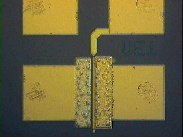


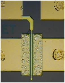
4 Micrographs With Field Plate: Without Field Plate: G G D S D S 4

5 Device Schematic & TEM result Pt deposition Field Plate Ohmic source contact Gate SiN x passivation Ohmic drain conta ield Plate GaN Phase nucleating at interface 1µm S Pt SiNx D AlGaN/GaN 5
6 Drain I-V Characteristics (ma) V G = V Step =.5V NFP FP (ma/mm) V DS 6
7 Off-state Stress Result I G (ma/mm) NFP FP I G (A) V GS V cri -7 7
 Electric Field (MV/cm) 3. 2.5 2. 1.5 1.")
8 Electric Field Simulation 2- D simula8on of the electric field distribu8on between Source and Drain. ATLAS/BLAZE (AutomaGcally tuned linear algebra sohware) Electric Field (MV/cm) S G No F ield P late F ield P late Vg=- 5V V DS =3V Position (µm) D 8
9 I G, I GS and I GD as a function of V GS I G - 4 I GS Ig (ma/mm) I GD Vcrit Ig (A) V GS - 8 9


10 TEM Result Fresh device Stressed device Source side of gate edge Drain side of gate edge Dr. Smith, ASU
11 TEM Result Au Ni AlGaN Metal diffusion GaN TD 11
12 STEM-EELS Line Scan a a Distance (nm) b Ni N O Ni c Counts ( 5 ) b Distance (nm) N O Ni Counts ( 5 ) c N O Ni nm AlGaN Distance (nm) 12

13 Field-plate Conclusions By employing Source field plate the device s cri8cal voltage has been improved from - 4 to - 65V, and breakdown voltage from 5 to 15V. 13
 Ig (A) 14")
14 DC characteristics of Pt- and Ni-gated HEMTs (ma/mm) Ni/Au gate Pt/Ti/Au gate V DS (ma) Ig (ma/mm) Ig (ma/mm) -2 Reverse Bias Pt/Ti/Au gate Ni/Au gate Forward Bias Vg Ni/Au gate P t/ti/au gate Ig (A) Ig (A) 14
15 Comparison of V cri I G (ma/mm) Ni- gated HEMTs V DS = +5V I G (A) I G (ma/mm) 3 Pt- gated HEMTs 1 V DS = +5V V GS V GS 15
16 Comparison of Drain I-V (ma/mm) Ni- g ated H E MT s F resh S tressed V G = V, step = - 1V (ma) (ma/mm) P t- g ated H E MT s F resh S tressed V G = V, step = - 1V V DS V DS 16
17 omparison of Gate leakage current Ig (ma/mm) Reverse Bias Pt- gate Ni- gate F resh S tressed V G Ig (A) Ig (ma/mm) Pt- gate V G Forward Bias Ni- gate F resh S tressed
18 omparison of sub-threshold leakage current (ma/mm) V DS = V 2V 3V 4V Ni- g ated H E MT s V GS (A) (ma/mm) V DS = V 2V 3V 4V Pt- gated HEMTs V GS
19 omparison of ON/OFF ratio, I G (ma/mm) 6 Fresh Stressed I G V DS = +4V Ni- gated HEMTs V G , I G (A), I G (ma/mm) 6 Fresh Stressed P t- g ated H E MT s I G V DS = +4V V G , I G (A) 19
20 ummary of parameters before/after stress Pt/Ti/Au Ni/Au Subthreshold slope (mv/dec) On/Off ra8o Ideality factor Scho]ky barrier height Fresh Stressed Fresh Stressed
21 XPS results As deposit Post annealed 5 Pt on GaN As deposit 1.Pt 4f 7/2 5 Pt on GaN 4 Post-anneal 1.Pt 4f 7/2 Intensity N(E) Pt 4f 5/2 Intensity N(E) Pt 4f 5/ Binding Energy (ev) Binding Energy (ev) 21
22 XPS results As deposit Post annealed Intensity N(E) Ni on GaN As deposit 1.Ni-O 2.Ni satellite 3.Ni metal Intensity N(E) Ni on GaN 1 Post-anneal 1.Ni-O 2.Ni satellite 3.Ni metal Binding Energy (ev) Binding Energy (ev) 22
23 XPS results As deposit Post annealed Intensity N(E) Ni on GaN 2 1 As deposit 1.Ga-O 2.Ni-O (e) Ni on GaN 2 1 Post-anneal 1.Ga-O 2.Ni-O (f) Binding Energy (ev) Binding Energy (ev) 23

24 Pt gate Conclusion Using Pt gate metalliza8on, the cri8cal voltage of electrical stress has been enhanced from - 55V with Ni gate to greater than - V with Pt gate. The reliability of AlGaN/GaN HEMTs have been enhanced significantly. 24
Fundamental Failure Mechanisms Limiting Maximum Voltage Operation in AlGaN/GaN HEMTs. Michael D. Hodge, Ramakrishna Vetury, and Jeffrey B.
 Fundamental Failure Mechanisms Limiting Maximum Voltage Operation in AlGaN/GaN HEMTs Michael D. Hodge, Ramakrishna Vetury, and Jeffrey B. Shealy Purpose Propose a method of determining Safe Operating Area
AlGaN/GaN High-Electron-Mobility Transistor Using a Trench Structure for High-Voltage Switching Applications
 Applied Physics Research; Vol. 4, No. 4; 212 ISSN 19169639 EISSN 19169647 Published by Canadian Center of Science and Education AlGaN/GaN HighElectronMobility Transistor Using a Trench Structure for HighVoltage
Reverse gate bias-induced degradation of AlGaN/GaN high electron mobility transistors
 Reverse gate bias-induced degradation of AlGaN/GaN high electron mobility transistors Chih-Yang Chang Travis Anderson and Jennifer Hite U.S. Naval Research Laboratory, Washington, DC 20375 Liu Lu, Chien-Fong
Effective Channel Mobility of AlGaN/GaN-on-Si Recessed-MOS-HFETs
 JOURNAL OF SEMICONUCTOR TECHNOLOGY AN SCIENCE, VOL.16, NO.6, ECEMBER, 216 ISSN(Print) 1598-1657 https://doi.org/1.5573/jsts.216.16.6.867 ISSN(Online) 2233-4866 Effective Channel Mobility of AlGaN/GaN-on-Si
Sub-Threshold Region Behavior of Long Channel MOSFET
 Sub-threshold Region - So far, we have discussed the MOSFET behavior in linear region and saturation region - Sub-threshold region is refer to region where Vt is less than Vt - Sub-threshold region reflects
GaN power electronics
 GaN power electronics The MIT Faculty has made this article openly available. Please share how this access benefits you. Your story matters. Citation As Published Publisher Lu, Bin, Daniel Piedra, and
GaN MMIC PAs for MMW Applicaitons
 GaN MMIC PAs for MMW Applicaitons Miroslav Micovic HRL Laboratories LLC, 311 Malibu Canyon Road, Malibu, CA 9265, U. S. A. mmicovic@hrl.com Motivation for High Frequency Power sources 6 GHz 11 GHz Frequency
International Workshop on Nitride Semiconductors (IWN 2016)
") International Workshop on Nitride Semiconductors (IWN 2016) Sheng Jiang The University of Sheffield Introduction The 2016 International Workshop on Nitride Semiconductors (IWN 2016) conference is held
International Workshop on Nitride Semiconductors (IWN 2016) Sheng Jiang The University of Sheffield Introduction The 2016 International Workshop on Nitride Semiconductors (IWN 2016) conference is held
RADIATION RESPONSE AND RELIABILITY OF HIGH SPEED AlGaN/GaN HEMTS
 RADIATION RESPONSE AND RELIABILITY OF HIGH SPEED AlGaN/GaN HEMTS By Jin Chen Dissertation Submitted to the Faculty of the Graduate school of Vanderbilt University in partial fulfillment of the requirements
High Voltage Normally-off GaN MOSC- HEMTs on Silicon Substrates for Power Switching Applications
 High Voltage Normally-off GaN MOSC- HEMTs on Silicon Substrates for Power Switching Applications Zhongda Li, John Waldron, Shinya Takashima, Rohan Dayal, Leila Parsa, Mona Hella, and T. Paul Chow Department
Record Extrinsic Transconductance (2.45 ms/μm at V DS = 0.5 V) InAs/In 0.53 Ga 0.47 As Channel MOSFETs Using MOCVD Source-Drain Regrowth
 InAs/In 0.53 Ga 0.47 As Channel MOSFETs Using MOCVD Source-Drain Regrowth") Record Extrinsic Transconductance (2.45 ms/μm at = 0.5 V) InAs/In 0.53 Ga 7 As Channel MOSFETs Using MOCVD Source-Drain Regrowth Sanghoon Lee 1*, C.-Y. Huang 1, A. D. Carter 1, D. C. Elias 1, J. J. M.
Record Extrinsic Transconductance (2.45 ms/μm at = 0.5 V) InAs/In 0.53 Ga 7 As Channel MOSFETs Using MOCVD Source-Drain Regrowth Sanghoon Lee 1*, C.-Y. Huang 1, A. D. Carter 1, D. C. Elias 1, J. J. M.
Novel III-Nitride HEMTs
 IEEE EDS Distinguished Lecture Boston Chapter, July 6 2005 Novel III-Nitride HEMTs Professor Kei May Lau Department of Electrical and Electronic Engineering Hong Kong University of Science and Technology
Semiconductor Materials for Power Electronics (SEMPEL) GaN power electronics materials
 GaN power electronics materials") Semiconductor Materials for Power Electronics (SEMPEL) GaN power electronics materials Kjeld Pedersen Department of Physics and Nanotechnology, AAU SEMPEL Semiconductor Materials for Power Electronics
Semiconductor Materials for Power Electronics (SEMPEL) GaN power electronics materials Kjeld Pedersen Department of Physics and Nanotechnology, AAU SEMPEL Semiconductor Materials for Power Electronics
NAME: Last First Signature
 UNIVERSITY OF CALIFORNIA, BERKELEY College of Engineering Department of Electrical Engineering and Computer Sciences EE 130: IC Devices Spring 2003 FINAL EXAMINATION NAME: Last First Signature STUDENT
RADIATION RESPONSE AND RELIABILITY OF AlGaN/GaN HEMTS
 RADIATION RESPONSE AND RELIABILITY OF AlGaN/GaN HEMTS By Jin Chen Thesis Submitted to the Faculty of the Graduate school of Vanderbilt University in partial fulfillment of the requirements For the degree
Customized probe card for on-wafer testing of AlGaN/GaN power transistors
 Customized probe card for on-wafer testing of AlGaN/GaN power transistors R. Venegas 1, K. Armendariz 2, N. Ronchi 1 1 imec, 2 Celadon Systems Inc. Outline Introduction GaN for power switching applications
Power. GaN. Rdyn in hard and soft-switching applications. P. Gassot, P. Moens, M. Tack, Corporate R&D Bodo Power Conference Munich, Dec.
 Power GaN Rdyn in hard and soft-switching applications P. Gassot, P. Moens, M. Tack, Corporate R&D Bodo Power Conference Munich, Dec. 2017 Acknowledgements The authors wish to acknowledge and thank the
Acknowledgments: This work was supported by Air Force HiREV program and the DTRA Basic Research Program.
 Gate Bias and Geometry Dependence of Total-Ionizing-Dose Effects in InGaAs Quantum-Well MOSFETs K. Ni 1, E. X. Zhang 1, R. D. Schrimpf 1, D. M. Fleetwood 1, R. A. Reed 1, M. L. Alles 1, J. Lin 2, and J.
AlGaN Polarization Graded Field Effect Transistors for High Linearity Microwave Applications
 AlGaN Polarization Graded Field Effect Transistors for High Linearity Microwave Applications Shahadat H. Sohel, Hao Xue, Towhidur Razzak, Sanyam Bajaj, Yuewei Zhang, Wu Lu, Siddharth Rajan Department of
Customized probe card for on wafer testing of AlGaN/GaN power transistors
 Customized probe card for on wafer testing of AlGaN/GaN power transistors R. Venegas 1, K. Armendariz 2, N. Ronchi 1 1 imec, 2 Celadon Systems Inc. Presented by Bryan Root 2 Outline Introduction GaN for
We are right on schedule for this deliverable. 4.1 Introduction:
 DELIVERABLE # 4: GaN Devices Faculty: Dipankar Saha, Subhabrata Dhar, Subhananda Chakrabati, J Vasi Researchers & Students: Sreenivas Subramanian, Tarakeshwar C. Patil, A. Mukherjee, A. Ghosh, Prantik
4: Transistors Non idealities
 4: Transistors Non idealities Inversion Major cause of non-idealities/complexities: Who controls channel (and how)? Large Body(Substrate) Source Voltage V G V SB - - - - - - - - n+ n+ - - - - - - - - -
Gallium nitride (GaN)
") 80 Technology focus: GaN power electronics Vertical, CMOS and dual-gate approaches to gallium nitride power electronics US research company HRL Laboratories has published a number of papers concerning
80 Technology focus: GaN power electronics Vertical, CMOS and dual-gate approaches to gallium nitride power electronics US research company HRL Laboratories has published a number of papers concerning
Deprocessing and defect analysis of GaN/AlGaN HEMTs. Patrick Whiting, Ray Holzworth Dr. Nicholas Rudawski, and Dr. Kevin Jones
 Deprocessing and defect analysis of GaN/AlGaN HEMTs Patrick Whiting, Ray Holzworth Dr. Nicholas Rudawski, and Dr. Kevin Jones Scientific Approach FLOORS TEM SEM SEM LEAP t=0, As Built TEM OSTS Gate Metal
A New Self-aligned Quantum-Well MOSFET Architecture Fabricated by a Scalable Tight-Pitch Process
 A New Self-aligned Quantum-Well MOSFET Architecture Fabricated by a Scalable Tight-Pitch Process Jianqiang Lin, Xin Zhao, Tao Yu, Dimitri A. Antoniadis, and Jesús A. del Alamo Microsystems Technology Laboratories,
InGaAs MOSFETs for CMOS:
 InGaAs MOSFETs for CMOS: Recent Advances in Process Technology J. A. del Alamo, D. Antoniadis, A. Guo, D.-H. Kim 1, T.-W. Kim 2, J. Lin, W. Lu, A. Vardi and X. Zhao Microsystems Technology Laboratories,
Normally-Off Operation of AlGaN/GaN Heterojunction Field-Effect Transistor with Clamping Diode
 JOURNAL OF SEMICONDUCTOR TECHNOLOGY AND SCIENCE, VOL.16, NO.2, APRIL, 2016 ISSN(Print) 1598-1657 http://dx.doi.org/10.5573/jsts.2016.16.2.221 ISSN(Online) 2233-4866 Normally-Off Operation of AlGaN/GaN
Design of Enhancement Mode Single-gate and Double-gate Multi-channel GaN HEMT with Vertical Polarity Inversion Heterostructure
 MITSUBISHI ELECTRIC RESEARCH LABORATORIES http://www.merl.com Design of Enhancement Mode Single-gate and Double-gate Multi-channel GaN HEMT with Vertical Polarity Inversion Heterostructure Feng, P.; Teo,
FABRICATION OF SELF-ALIGNED T-GATE AlGaN/GaN HIGH
 International Journal of High Speed Electronics and Systems World Scientific Vol. 14, No. 3 (24) 85-89 wworldscientific World Scientific Publishing Company www.worldsclentific.com FABRICATION OF SELF-ALIGNED
3: MOS Transistors. Non idealities
 3: MOS Transistors Non idealities Inversion Major cause of non-idealities/complexities: Who controls channel (and how)? Large Body(Substrate) Source Voltage V G V SB - - - - - - - - n+ n+ - - - - - - -
E-MODE III-N HIGH-VOLTAGE TRANSISTOR DEVELOPMENT
 1 E-MODE III-N HIGH-VOLTAGE TRANSISTOR DEVELOPMENT 1 st -Year Final Project Report (Feb 2010 March 2011) Presented to Intersil Corp., Milpitas CA Program Manager: Dr. François Hébert Georgia Tech PIs:
3-D Modelling of the Novel Nanoscale Screen-Grid Field Effect Transistor (SGFET)
") 3-D Modelling of the Novel Nanoscale Screen-Grid Field Effect Transistor (SGFET) Pei W. Ding, Kristel Fobelets Department of Electrical Engineering, Imperial College London, U.K. J. E. Velazquez-Perez
3-D Modelling of the Novel Nanoscale Screen-Grid Field Effect Transistor (SGFET) Pei W. Ding, Kristel Fobelets Department of Electrical Engineering, Imperial College London, U.K. J. E. Velazquez-Perez
CHAPTER 8 FIELD EFFECT TRANSISTOR (FETs)
") CHAPTER 8 FIELD EFFECT TRANSISTOR (FETs) INTRODUCTION - FETs are voltage controlled devices as opposed to BJT which are current controlled. - There are two types of FETs. o Junction FET (JFET) o Metal
CHAPTER 8 FIELD EFFECT TRANSISTOR (FETs) INTRODUCTION - FETs are voltage controlled devices as opposed to BJT which are current controlled. - There are two types of FETs. o Junction FET (JFET) o Metal
Enhancement-mode AlGaN/GaN HEMTs on silicon substrate
 phys. stat. sol. (c) 3, No. 6, 368 37 (6) / DOI 1.1/pssc.565119 Enhancement-mode AlGaN/GaN HEMTs on silicon substrate Shuo Jia, Yong Cai, Deliang Wang, Baoshun Zhang, Kei May Lau, and Kevin J. Chen * Department
GaN: Applications: Optoelectronics
 GaN: Applications: Optoelectronics GaN: Applications: Optoelectronics - The GaN LED industry is >10 billion $ today. - Other optoelectronic applications of GaN include blue lasers and UV emitters and detectors.
Field-Effect Transistor (FET) is one of the two major transistors; FET derives its name from its working mechanism;
 is one of the two major transistors; FET derives its name from its working mechanism;") Chapter 3 Field-Effect Transistors (FETs) 3.1 Introduction Field-Effect Transistor (FET) is one of the two major transistors; FET derives its name from its working mechanism; The concept has been known
Chapter 3 Field-Effect Transistors (FETs) 3.1 Introduction Field-Effect Transistor (FET) is one of the two major transistors; FET derives its name from its working mechanism; The concept has been known
I E I C since I B is very small
 Figure 2: Symbols and nomenclature of a (a) npn and (b) pnp transistor. The BJT consists of three regions, emitter, base, and collector. The emitter and collector are usually of one type of doping, while
MOSFET short channel effects
 MOSFET short channel effects overview Five different short channel effects can be distinguished: velocity saturation drain induced barrier lowering (DIBL) impact ionization surface scattering hot electrons
SEVERAL III-V materials, due to their high electron
 IEEE TRANSACTIONS ON NUCLEAR SCIENCE, VOL. 64, NO. 1, JANUARY 2017 239 Gate Bias and Geometry Dependence of Total-Ionizing-Dose Effects in InGaAs Quantum-Well MOSFETs Kai Ni, Student Member, IEEE, En Xia
832 IEEE TRANSACTIONS ON ELECTRON DEVICES, VOL. 64, NO. 3, MARCH 2017
 832 IEEE TRANSACTIONS ON ELECTRON DEVICES, VOL. 64, NO. 3, MARCH 2017 Investigation of In Situ SiN as Gate Dielectric and Surface Passivation for GaN MISHEMTs Huaxing Jiang, Chao Liu, Yuying Chen, Xing
Scaling and High-Frequency Performance of AlN/GaN HEMTs
 Scaling and High-Frequency Performance of AlN/GaN HEMTs Xi Luo 1, Subrata Halder 1, Walter R. Curtice 1, James C. M. Hwang 1, Kelson D. Chabak 2, Dennis E. Walker, Jr. 2, and Amir M. Dabiran 3 1 Lehigh
Composants HEMT InAlGaN/GaN pour applications en bandes Ka et Q.
 Composants HEMT InAlGaN/GaN pour applications en bandes Ka et Q. Stéphane PIOTROWICZ, Olivier PATARD, Jean-Claude JACQUET, Piero GAMARRA, Christian DUA & Sylvain DELAGE RF & Microwave 22 mars 2018 Copyright
III-Nitride microwave switches Grigory Simin
 Microwave Microelectronics Laboratory Department of Electrical Engineering, USC Research Focus: - Wide Bandgap Microwave Power Devices and Integrated Circuits - Physics, Simulation, Design and Characterization
RF Power Degradation of GaN High Electron Mobility Transistors
 RF Power Degradation of GaN High Electron Mobility Transistors The MIT Faculty has made this article openly available. Please share how this access benefits you. Your story matters. Citation As Published
GaN based Power Devices. Michael A. Briere. RPI CFES Conference
 GaN based Power Devices Michael A. Briere ACOO Enterprises LLC Under contract to International Rectifier RPI CFES Conference January 25, 2013 1 Motivation : Potential Energy Savings Worldwide M.A. Briere
CHAPTER 2 HEMT DEVICES AND BACKGROUND
 CHAPTER 2 HEMT DEVICES AND BACKGROUND 2.1 Overview While the most widespread application of GaN-based devices is in the fabrication of blue and UV LEDs, the fabrication of microwave power devices has attracted
Chapter 1. Introduction
 Chapter 1 Introduction 1.1 Introduction of Device Technology Digital wireless communication system has become more and more popular in recent years due to its capability for both voice and data communication.
Bias Stress Testing of SiC MOSFETs
 Bias Stress Testing of SiC MOSFETs Robert Shaw Manager, Test and Qualification August 15 th, 2014 Special thanks to the U.S. Department of Energy for funding this under SBIR DE-SC0011315. Outline Objectives
PRELIMINARY = 25 C) Parameter GHz 14.0 GHz 14.5 GHz Units Small Signal Gain db P SAT. = 26 dbm W P 3dB
 Parameter GHz 14.0 GHz 14.5 GHz Units Small Signal Gain db P SAT. = 26 dbm W P 3dB") CMPADE030D PRELIMINARY 30 W, 3.75-4.5 GHz, 40 V, GaN MMIC, Power Amplifier Cree s CMPADE030D is a gallium nitride (GaN) High Electron Mobility Transistor (HEMT) based monolithic microwave integrated circuit
CMPADE030D PRELIMINARY 30 W, 3.75-4.5 GHz, 40 V, GaN MMIC, Power Amplifier Cree s CMPADE030D is a gallium nitride (GaN) High Electron Mobility Transistor (HEMT) based monolithic microwave integrated circuit
Record I on (0.50 ma/μm at V DD = 0.5 V and I off = 100 na/μm) 25 nm-gate-length ZrO 2 /InAs/InAlAs MOSFETs
 25 nm-gate-length ZrO 2 /InAs/InAlAs MOSFETs") Record I on (0.50 ma/μm at V DD = 0.5 V and I off = 100 na/μm) 25 nm-gate-length ZrO 2 /InAs/InAlAs MOSFETs Sanghoon Lee 1*, V. Chobpattana 2,C.-Y. Huang 1, B. J. Thibeault 1, W. Mitchell 1, S. Stemmer
Record I on (0.50 ma/μm at V DD = 0.5 V and I off = 100 na/μm) 25 nm-gate-length ZrO 2 /InAs/InAlAs MOSFETs Sanghoon Lee 1*, V. Chobpattana 2,C.-Y. Huang 1, B. J. Thibeault 1, W. Mitchell 1, S. Stemmer
UNIVERSITY OF CALIFORNIA AT BERKELEY College of Engineering Department of Electrical Engineering and Computer Sciences.
 UNIVERSITY OF CALIFORNIA AT BERKELEY College of Engineering Department of Electrical Engineering and Computer Sciences Discussion #9 EE 05 Spring 2008 Prof. u MOSFETs The standard MOSFET structure is shown
Wu Lu Department of Electrical and Computer Engineering and Microelectronics Laboratory, University of Illinois, Urbana, Illinois 61801
 Comparative study of self-aligned and nonself-aligned SiGe p-metal oxide semiconductor modulation-doped field effect transistors with nanometer gate lengths Wu Lu Department of Electrical and Computer
New Generation Reliability Model
 New Generation Reliability Model S.-Y. Liao, C. Huang, T. Guo, A. Chen, Jushan Xie, Cadence Design Systems, Inc. S. Guo, R. Wang, Z. Yu, P. Hao, P. Ren, Y. Wang, R. Huang, Peking University Dec. 5th, 2016
Atomic-layer deposition of ultrathin gate dielectrics and Si new functional devices
 Atomic-layer deposition of ultrathin gate dielectrics and Si new functional devices Anri Nakajima Research Center for Nanodevices and Systems, Hiroshima University 1-4-2 Kagamiyama, Higashi-Hiroshima,
Research Article GaN-Based High-k Praseodymium Oxide Gate MISFETs with P 2 S 5 /(NH 4 ) 2 S X + UV Interface Treatment Technology
 2 S X + UV Interface Treatment Technology") Active and Passive Electronic Components Volume, Article ID 9, pages doi:.//9 Research Article GaN-Based High-k Praseodymium Oxide Gate MISFETs with P S /(NH S X + UV Interface Treatment Technology Chao-Wei
Active and Passive Electronic Components Volume, Article ID 9, pages doi:.//9 Research Article GaN-Based High-k Praseodymium Oxide Gate MISFETs with P S /(NH S X + UV Interface Treatment Technology Chao-Wei
Modeling the Influence of Dielectric Interface Traps on I-V Characteristics of TFETs
 Modeling the Influence of Dielectric Interface Traps on I-V Characteristics of TFETs Jie Min 1, Peter Asbeck UCSD 1 Present address: Global Foundries, Santa Clara, CA Schematic TFET Structures Based on
Y9.FS1.2.1: GaN Low Voltage Power Device Development. Sizhen Wang (Ph.D., EE)
") Y9.FS1.2.1: GaN Low Voltage Power Device Development Faculty: Students: Alex. Q. Huang Sizhen Wang (Ph.D., EE) 1. Project Goals The overall objective of the GaN power device project is to fabricate and
Y9.FS1.2.1: GaN Low Voltage Power Device Development Faculty: Students: Alex. Q. Huang Sizhen Wang (Ph.D., EE) 1. Project Goals The overall objective of the GaN power device project is to fabricate and
Ceramic Packaged GaAs Power phemt DC-12 GHz
 Ceramic Packaged GaAs Power phemt DC-12 GHz DESCRIPTION AMCOM s is a discrete GaAs phemt that has a total gate width of 1.mm. It is in a ceramic BH package for operating up to 12 GHz. The BH package has
DC AND SMALL SIGNAL DEGRADATION IN INAS - ALSB HEMTS UNDER HOT CARRIER STRESS. Sandeepan DasGupta. Dissertation. Submitted to the Faculty of the
 DC AND SMALL SIGNAL DEGRADATION IN INAS - ALSB HEMTS UNDER HOT CARRIER STRESS By Sandeepan DasGupta Dissertation Submitted to the Faculty of the Graduate School of Vanderbilt University in partial fulfillment
Development of Microwave and Terahertz Detectors Utilizing AlN/GaN High Electron Mobility Transistors
 Development of Microwave and Terahertz Detectors Utilizing AlN/GaN High Electron Mobility Transistors L. Liu 1, 2,*, B. Sensale-Rodriguez 1, Z. Zhang 1, T. Zimmermann 1, Y. Cao 1, D. Jena 1, P. Fay 1,
Microwave & RF 22 nd of March 2018 D. FLORIOT
 Microwave & RF 22 nd of March 2018 D. FLORIOT Outine Introduction GaN technology roadmap GH15-10 : Up to Ka band GH10 : Towards high frequency (Q / V bands) GaN : Technology & Integration 2 UMS at a glance
Fabrication of High-Power AlGaN/GaN Schottky Barrier Diode with Field Plate Design
 Fabrication of High-Power AlGaN/GaN Schottky Barrier Diode with Field Plate Design Chia-Jui Yu, Chien-Ju Chen, Jyun-Hao Liao, Chia-Ching Wu, Meng-Chyi Wu Abstract In this letter, we demonstrate high-performance
600V GaN Power Transistor
 600V GaN Power Transistor Sample Available Features Normally-Off Current-Collapse-Free Zero Recovery GaN Power Transistor (TO220 Package) ID(Continuous) : 15A RDS(on) : 65m Qg : 11nC Applications Power
Electronic Circuits. Junction Field-effect Transistors. Dr. Manar Mohaisen Office: F208 Department of EECE
 Electronic Circuits Junction Field-effect Transistors Dr. Manar Mohaisen Office: F208 Email: manar.subhi@kut.ac.kr Department of EECE Review of the Precedent Lecture Explain the Operation Class A Power
A 2.4GHz Fully Integrated CMOS Power Amplifier Using Capacitive Cross-Coupling
 A 2.4GHz Fully Integrated CMOS Power Amplifier Using Capacitive Cross-Coupling JeeYoung Hong, Daisuke Imanishi, Kenichi Okada, and Akira Tokyo Institute of Technology, Japan Contents 1 Introduction PA
Sub-30 nm InAs Quantum-Well MOSFETs with Self-Aligned Metal Contacts and Sub-1 nm EOT HfO 2 Insulator
 Sub-30 nm InAs Quantum-Well MOSFETs with Self-Aligned Metal Contacts and Sub-1 nm EOT HfO 2 Insulator Jianqiang Lin, Dimitri A. Antoniadis, and Jesús A. del Alamo Microsystems Technology Laboratories,
INVESTIGATION OF DEGRADATION EFFECTS DUE TO GATE STRESS. IN GaN-ON-Si HIGH ELECTRON MOBILITY TRANSISTORS THROUGH ANALYSIS OF LOW FREQUENCY NOISE
 INVESTIGATION OF DEGRADATION EFFECTS DUE TO GATE STRESS IN GaN-ON-Si HIGH ELECTRON MOBILITY TRANSISTORS THROUGH ANALYSIS OF LOW FREQUENCY NOISE A Thesis presented to the Faculty of California Polytechnic
Carbon Nanotube Bumps for Thermal and Electric Conduction in Transistor
 Carbon Nanotube Bumps for Thermal and Electric Conduction in Transistor V Taisuke Iwai V Yuji Awano (Manuscript received April 9, 07) The continuous miniaturization of semiconductor chips has rapidly improved
TEST FREQ. 12 GHz 18 GHz 12 GHz 18 GHz. P1dB Output p1db (Vds = 2V, Id = 10mA) 12 GHz dbm
 12 GHz dbm") SUPER LOW NOISE PHEMT CHIP (.15µm x 160µm) The BeRex BCL016B is a GaAs super low noise phemt with a nominal 0.15 micron gate length and 160 micron gate width making the product ideally suited for applications
SUPER LOW NOISE PHEMT CHIP (.15µm x 160µm) The BeRex BCL016B is a GaAs super low noise phemt with a nominal 0.15 micron gate length and 160 micron gate width making the product ideally suited for applications
8. Characteristics of Field Effect Transistor (MOSFET)
") 1 8. Characteristics of Field Effect Transistor (MOSFET) 8.1. Objectives The purpose of this experiment is to measure input and output characteristics of n-channel and p- channel field effect transistors
1 8. Characteristics of Field Effect Transistor (MOSFET) 8.1. Objectives The purpose of this experiment is to measure input and output characteristics of n-channel and p- channel field effect transistors
Solid State Device Fundamentals
 Solid State Device Fundamentals 4.4. Field Effect Transistor (MOSFET) ENS 463 Lecture Course by Alexander M. Zaitsev alexander.zaitsev@csi.cuny.edu Tel: 718 982 2812 4N101b 1 Field-effect transistor (FET)
PERSPECTIVES FOR DISRUPTIVE 200MM/8-INCH GAN POWER DEVICE AND GAN-IC TECHNOLOGY DR. DENIS MARCON SR. BUSINESS DEVELOPMENT MANAGER
 PERSPECTIVES FOR DISRUPTIVE 200MM/8-INCH GAN POWER DEVICE AND GAN-IC TECHNOLOGY DR. DENIS MARCON SR. BUSINESS DEVELOPMENT MANAGER What I will show you today 200mm/8-inch GaN-on-Si e-mode/normally-off technology
AlGaN/GaN metal-insulator-semiconductor heterojunction field-effect transistors using BN and AlTiO high-k gate insulators
 AlGaN/GaN metal-insulator-semiconductor heterojunction field-effect transistors using BN and AlTiO high-k gate insulators NGUYEN QUY TUAN Japan Advanced Institute of Science and Technology Doctoral Dissertation
CHARACTERIZATION OF GaN MOS-HEMT TRAP- RELATED EFFECTS FOR POWER SWITCHING APPLICATIONS
 CHARACTERIZATION OF GaN MOS-HEMT TRAP- RELATED EFFECTS FOR POWER SWITCHING APPLICATIONS BY DABIN ZHANG THESIS Submitted in partial fulfillment of the requirements for the degree of Master of Science in
Defense Technical Information Center Compilation Part Notice
 UNCLASSIFIED Defense Technical Information Center Compilation Part Notice ADP015074 TITLE: Channel Recessed 4H-SiC MESFETs with Ft o f14.5ghz and F max of 40GHz DISTRIBUTION: Approved for public release,
Self-Aligned-Gate GaN-HEMTs with Heavily-Doped n + -GaN Ohmic Contacts to 2DEG
 Self-Aligned-Gate GaN-HEMTs with Heavily-Doped n + -GaN Ohmic Contacts to 2DEG K. Shinohara, D. Regan, A. Corrion, D. Brown, Y. Tang, J. Wong, G. Candia, A. Schmitz, H. Fung, S. Kim, and M. Micovic HRL
ASM GaN HEMT: Advanced SPICE Model for GaN HEMTs
 ASM GaN HEMT: Advanced SPICE Model for GaN HEMTs Sourabh Khandelwal, T. A. Fjeldly, B. Iniguez, Y. S. Chauhan, S. Ghosh, A. Dasgupta MOS-AK 2014 Sourabh Khandelwal MOS-AK 2014 1 Outline ASM-HEMT Model
Students: Yifan Jiang (Research Assistant) Siyang Liu (Visiting Scholar)
 Siyang Liu (Visiting Scholar)") Y9.FS1.1: SiC Power Devices for SST Applications Project Leader: Faculty: Dr. Jayant Baliga Dr. Alex Huang Students: Yifan Jiang (Research Assistant) Siyang Liu (Visiting Scholar) 1. Project Goals (a)
Y9.FS1.1: SiC Power Devices for SST Applications Project Leader: Faculty: Dr. Jayant Baliga Dr. Alex Huang Students: Yifan Jiang (Research Assistant) Siyang Liu (Visiting Scholar) 1. Project Goals (a)
EE241 - Spring 2013 Advanced Digital Integrated Circuits. Projects. Groups of 3 Proposals in two weeks (2/20) Topics: Lecture 5: Transistor Models
 Topics: Lecture 5: Transistor Models") EE241 - Spring 2013 Advanced Digital Integrated Circuits Lecture 5: Transistor Models Projects Groups of 3 Proposals in two weeks (2/20) Topics: Soft errors in datapaths Soft errors in memory Integration
EE241 - Spring 2013 Advanced Digital Integrated Circuits Lecture 5: Transistor Models Projects Groups of 3 Proposals in two weeks (2/20) Topics: Soft errors in datapaths Soft errors in memory Integration
CHAPTER I INTRODUCTION. mechanisms for the device are yet to be adequately understood. In this thesis, a detailed
 CHAPTER I INTRODUCTION Indium Arsenide (InAs) channel high electron mobility transistors (HEMTs) with Aluminium Antimonide (AlSb) barriers are an exciting option for low power RF applications due to excellent
A new Hetero-material Stepped Gate (HSG) SOI LDMOS for RF Power Amplifier Applications
 SOI LDMOS for RF Power Amplifier Applications") A new Hetero-material Stepped Gate (HSG) SOI LDMOS for RF Power Amplifier Applications Radhakrishnan Sithanandam and M. Jagadesh Kumar, Senior Member, IEEE Department of Electrical Engineering Indian Institute
A new Hetero-material Stepped Gate (HSG) SOI LDMOS for RF Power Amplifier Applications Radhakrishnan Sithanandam and M. Jagadesh Kumar, Senior Member, IEEE Department of Electrical Engineering Indian Institute
FP Description. Features. Applications. Packaging Information. 340W, 48V GaN HEMT D
 FP48005340 340W, 48V GaN HEMT D Description The FP48005340 is a 340W gallium nitride (GaN) High Electron Mobility Transistor (HEMT). This GaN HEMT is a wideband transistor optimized for 3.5GHz operation
FP Description. Features. Applications. Packaging Information. 260W, 48V GaN HEMT D
 FP48005260 260W, 48V GaN HEMT D Description The FP48005260 is a 260W gallium nitride (GaN) High Electron Mobility Transistor (HEMT). This GaN HEMT is a wideband transistor optimized for 3.5GHz operation
A Gate Sinking Threshold Voltage Adjustment Technique for High Voltage GaN HEMT
 A Gate Sinking Threshold Voltage Adjustment Technique for High Voltage GaN HEMT by WeiJia Zhang A thesis submitted in conformity with the requirements for the degree of Master of Applied Science Graduate
Parasitic Resistance Effects on Mobility Extraction of Normally-off AlGaN/GaN Gate-recessed MISHFETs
 JOURNAL OF SEMICONDUCTOR TECHNOLOGY AND SCIENCE, VOL.18, NO.1, FEBRUARY, 2018 ISSN(Print) 1598-1657 https://doi.org/10.5573/jsts.2018.18.1.078 ISSN(Online) 2233-4866 Parasitic Resistance Effects on Mobility
FP Description. Features. Applications. Packaging Information. 50W, 28V GaN HEMT Die
 FP28010060 50W, 28V GaN HEMT Die Description The FP28010060 is a 50W gallium nitride (GaN) High Electron Mobility Transistor (HEMT). This GaN HEMT is a wideband transistor optimized for X-band operation
Lecture (03) The JFET
 The JFET") Lecture (03) The JFET By: Dr. Ahmed ElShafee ١ JFET Basic Structure Figure shows the basic structure of an n channel JFET (junction field effect transistor). Wire leads are connected to each end of the
Lecture (03) The JFET By: Dr. Ahmed ElShafee ١ JFET Basic Structure Figure shows the basic structure of an n channel JFET (junction field effect transistor). Wire leads are connected to each end of the
Forming Gas Post Metallization Annealing of Recessed AlGaN/GaN-on-Si MOSHFET
 http://dx.doi.org/10.5573/jsts.2015.15.1.016 JOURNAL OF SEMICONDUCTOR TECHNOLOGY AND SCIENCE, VOL.15, NO.1, FEBRUARY, 2015 Forming Gas Post Metallization Annealing of Recessed AlGaN/GaN-on-Si MOSHFET Jung-Yeon
IFB270 Advanced Electronic Circuits
 IFB270 Advanced Electronic Circuits Chapter 9: FET amplifiers and switching circuits Prof. Manar Mohaisen Department of EEC Engineering Review of the Precedent Lecture Review of basic electronic devices
FP Description. Features. Applications. Packaging Information. 104W, 48V GaN HEMT D
 FP48007104 104W, 48V GaN HEMT D Description The FP48007104 is a 104W gallium nitride (GaN) High Electron Mobility Transistor (HEMT). This GaN HEMT is a wideband transistor optimized for 3.5GHz operation
Reliability Investigation of GaN HEMTs for MMICs Applications
 Micromachines 2014, 5, 570-582; doi:10.3390/mi5030570 Article OPEN ACCESS micromachines ISSN 2072-666X www.mdpi.com/journal/micromachines Reliability Investigation of GaN HEMTs for MMICs Applications Alessandro
On-Wafer Integration of Nitrides and Si Devices: Bringing the Power of Polarization to Si
 On-Wafer Integration of Nitrides and Si Devices: Bringing the Power of Polarization to Si The MIT Faculty has made this article openly available. Please share how this access benefits you. Your story matters.
UNIT 3: FIELD EFFECT TRANSISTORS
 FIELD EFFECT TRANSISTOR: UNIT 3: FIELD EFFECT TRANSISTORS The field effect transistor is a semiconductor device, which depends for its operation on the control of current by an electric field. There are
From Bulk Gallium Nitride Material to Vertical GaN Devices
 From Bulk Gallium Nitride Material to Vertical GaN Devices Thomas Mikolajick 1,2, Stefan Schmult 2, Rico Hentschel 1, Patrick Hofmann 1, and Andre Wachowiak 1 1 NaMLab ggmbh 2 Chair of Nanoelectronic Materials,
N-polar GaN/ AlGaN/ GaN high electron mobility transistors
 JOURNAL OF APPLIED PHYSICS 102, 044501 2007 N-polar GaN/ AlGaN/ GaN high electron mobility transistors Siddharth Rajan a Electrical and Computer Engineering Department, University of California, Santa
FET(Field Effect Transistor)
") Field Effect Transistor: Construction and Characteristic of JFETs. Transfer Characteristic. CS,CD,CG amplifier and analysis of CS amplifier MOSFET (Depletion and Enhancement) Type, Transfer Characteristic,
Field Effect Transistor: Construction and Characteristic of JFETs. Transfer Characteristic. CS,CD,CG amplifier and analysis of CS amplifier MOSFET (Depletion and Enhancement) Type, Transfer Characteristic,
III-V CMOS: Quo Vadis?
 III-V CMOS: Quo Vadis? J. A. del Alamo, X. Cai, W. Lu, A. Vardi, and X. Zhao Microsystems Technology Laboratories Massachusetts Institute of Technology Compound Semiconductor Week 2018 Cambridge, MA, May
MACOM GaN Reliability Presentation GaN on Silicon Processes and Products
 MACOM GaN Reliability Presentation GaN on Silicon Processes and Products 1 MACOM GaN on Silicon Reliability Presentation MACOM GaN Strategy GaN on Silicon Carbide 0.5um GaN HEMT process 0.25um GaN HEMT
High Power Wideband AlGaN/GaN HEMT Feedback. Amplifier Module with Drain and Feedback Loop. Inductances
 High Power Wideband AlGaN/GaN HEMT Feedback Amplifier Module with Drain and Feedback Loop Inductances Y. Chung, S. Cai, W. Lee, Y. Lin, C. P. Wen, Fellow, IEEE, K. L. Wang, Fellow, IEEE, and T. Itoh, Fellow,
Performance Analysis of 20 nm Pentagonal and Trapezoidal NanoWire Transistor with Si and Ge Channel
 Performance Analysis of 20 nm Pentagonal and Trapezoidal NanoWire Transistor with Si and Ge Channel SANDEEP SINGH GILL 1, JAIDEV KAUSHIK 2, NAVNEET KAUR 3 Department of Electronics and Communication Engineering