Electronics I Circuit Drawings. Robert R. Krchnavek Rowan University Spring, 2018
|
|
|
- Griffin Crawford
- 6 years ago
- Views:
Transcription
1 Electronics I Circuit Drawings Robert R. Krchnavek Rowan University Spring, 2018

2 Ideal Diode

3 Piecewise Linear Models of a Diode
4 Piecewise Linear Models of a Diode 1 r d
5 Piecewise Linear Models of a Diode

6 Piecewise Linear Models of a Diode V 0
7 Piecewise Linear Models of a Diode

8 Piecewise Linear Models of a Diode 1 r d V 0
9 Basic Diode Circuits v s
10 Basic Diode Circuits v L
11 Basic Diode Circuits v s

12 Basic Diode Circuits v L
13 Basic Diode Circuits v s


14 Basic Diode Circuits v L


15 Basic Diode Circuits Half-Wave Rectified Power Supply

16 Basic Diode Circuits v s
17 Basic Diode Circuits Replace the CT transformer with 2 sources. v s


18 Basic Diode Circuits v L

19 Basic Diode Circuits Adding the circuitry to the primary of the transformer and the capacitor to reduce ripple results in a conventional, full-wave rectifier power supply.


20 Basic Diode Circuits Reversing the diodes results in a negative output voltage (w.r.t. the reference node.) v s v L (assuming C = 0)

21 Basic Diode Circuits Combining the two circuits results in a bipolar supply one with a positive and negative output. One example of a use for a bipolar power supply is to power op amps.

22 Basic Diode Circuits Redrawing: bridge rectifier

23 Basic Diode Circuits You can produce a unipolar output power supply using a bridge rectifier and no center tap on the transformer. The output voltage will be twice as high as the bipolar supply for the same secondary voltage.

24 Sizing the Filter Capacitor v L

25 Zener-Diode Voltage Regulator
26 Basic Amplifiers
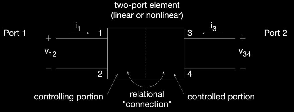
27 Basic Amplifers example element CCCS1 linear or non-linear?

28 Basic Amplifers Example CCCS1 Find: A v = v o v in

29 Basic Amplifers Modified Example CCCS1 Find: A v = v o v in
30 Basic Amplifiers Amplifier Parameters input impedance Z in = v in i in Usually done with the desired load attached to the circuit. output impedance Z out = Z o = v o i o Under specified source conditions with v s = 0. current gain A i = i out i in Under specified load conditions. power gain A p = P out P in Under specified load conditions.
31 Basic Amplifiers Biasing Biasing serves two purposes: it is the source of energy for power gain. it sets the device at a specific operating point for our desired application. It is the second bullet that we are most interested in.

32 Basic Amplifiers Biasing CCCS1 that we used to make our inverting amplifier Circuit to measure the v-i characteristics of the device.

33 Basic Amplifiers Biasing Circuit to measure the v-i characteristics of the device.
34 Basic Amplifiers Example

35 Basic Amplifiers Example Continued
36 <latexit sha1_base64="j58k4cplm3dmwicv8+6qcapjaus=">aaab83icbvdlsgnbejynrxhfuy9ebopgkeykob6ekfw8rnbnifmw2ulvmmt24uxviir8hxcpkl79gw/+jznkd5py0fbuddpdfarsalttb6uwtr6xuvxclu3s7u0fla+phnwskq4ut2si2ghtieumlgqu0e4vsciq0aqgjznfgohsiokfcjycf7f+lelbgrrje37jthsamir8ul+u2fv7drpknjxusi6mx/7q9hkerrajl0zrjmon6e2yqseltevdtepk+jd1ownozclq3mr+9jsegavhw0szipho1d8texzppy4c0xkxhohlbyb+53uydk+9iyjtdchmi0vhjikmdjya7qkfhoxyemavmldspmckctq5luwizvllq8s9qn5u7fvlsq2ep1ekj+sunbohxjeausnn4hjonsgzesvv1sh6sd6tj0vrwcpnjskfwj8/icyroq==</latexit> Bipolar Junction Transistors (BJTs) i C = i B (active region) To be in the Active Region: - base-emitter junction is forward-biased. - base-collector junction is reverse-biased.
")
37 Bipolar Junction Transistors (BJTs) NPN PNP
38 <latexit sha1_base64="herk2ovzsekvpyzul1jl0nzkt24=">aaab6xicbvbns8naej34wetx1aoxxsj4koki6q3ui8ekxhbaudbbtbt0swm7e6ge/gqvhls8+o+8+w/ctjlo64obx3szzmwluykmuu63s7k6tr6xwdoqb+/s7u1xdg4ftzjpxn2wyes3q2q4fir7kfdydqo5jupjw+hozuq3nrg2ilepoe55enobepfgfk10l3qnxqxq1twzydlxclkfas1e5avbt1gwc4vmumm6nptikfongkk+kxczw1pkrntao5yqgnmt5lntj+tukn0sjdqwqjjtf0/kndzmhie2m6y4nivevpzp62qyxqw5ugmgxlh5oiitbbmy/zv0heym5dgsyrswtxi2pjoytomubqje4svlxd+vxdfcu4tqvvgkuyjjoiez8oas6naltfcbwqce4rxehom8oo/ox7x1xslmjuapnm8ffaundq==</latexit> <latexit sha1_base64="herk2ovzsekvpyzul1jl0nzkt24=">aaab6xicbvbns8naej34wetx1aoxxsj4koki6q3ui8ekxhbaudbbtbt0swm7e6ge/gqvhls8+o+8+w/ctjlo64obx3szzmwluykmuu63s7k6tr6xwdoqb+/s7u1xdg4ftzjpxn2wyes3q2q4fir7kfdydqo5jupjw+hozuq3nrg2ilepoe55enobepfgfk10l3qnxqxq1twzydlxclkfas1e5avbt1gwc4vmumm6nptikfongkk+kxczw1pkrntao5yqgnmt5lntj+tukn0sjdqwqjjtf0/kndzmhie2m6y4nivevpzp62qyxqw5ugmgxlh5oiitbbmy/zv0heym5dgsyrswtxi2pjoytomubqje4svlxd+vxdfcu4tqvvgkuyjjoiez8oas6naltfcbwqce4rxehom8oo/ox7x1xslmjuapnm8ffaundq==</latexit> <latexit sha1_base64="herk2ovzsekvpyzul1jl0nzkt24=">aaab6xicbvbns8naej34wetx1aoxxsj4koki6q3ui8ekxhbaudbbtbt0swm7e6ge/gqvhls8+o+8+w/ctjlo64obx3szzmwluykmuu63s7k6tr6xwdoqb+/s7u1xdg4ftzjpxn2wyes3q2q4fir7kfdydqo5jupjw+hozuq3nrg2ilepoe55enobepfgfk10l3qnxqxq1twzydlxclkfas1e5avbt1gwc4vmumm6nptikfongkk+kxczw1pkrntao5yqgnmt5lntj+tukn0sjdqwqjjtf0/kndzmhie2m6y4nivevpzp62qyxqw5ugmgxlh5oiitbbmy/zv0heym5dgsyrswtxi2pjoytomubqje4svlxd+vxdfcu4tqvvgkuyjjoiez8oas6naltfcbwqce4rxehom8oo/ox7x1xslmjuapnm8ffaundq==</latexit> <latexit sha1_base64="nzfgys8++kgzl/cspytx+npspre=">aaab7hicbvbnswmxej2tx7v+vt16crbbu9kvqb2viucxgtsw2qvk02wbm02wjfsos/+dfw8qxv1b3vw3pu0etpxbwoo9gwbmhqln2rjut1nyw9/y3cpul3z29/ypyodhts1trahpjjeqhwjnorpun8xw2k4uxxhiassc3c781pgqzar4njoebjeecbyxgo2vmunevr+b9sovt+rogvajl5mk5gj0yl/dvirptiuhhgvd8dzebblwhhfop6vuqmmcyqgpamdsgwoqg2x+7rsdwawpiqlscypm6u+jdmdat+lqdsbydpwynxp/8zqpia6djikknvsqxaio5chinhsd9zmixpcjjzgozm9fzigvjsygvlihemsvrxl/onptdr8uk7v6nkyrtuauzsgdk6jbpttabwjp8ayv8ozi58v5dz4wrqunnzmgp3a+fwdily7d</latexit> <latexit sha1_base64="nzfgys8++kgzl/cspytx+npspre=">aaab7hicbvbnswmxej2tx7v+vt16crbbu9kvqb2viucxgtsw2qvk02wbm02wjfsos/+dfw8qxv1b3vw3pu0etpxbwoo9gwbmhqln2rjut1nyw9/y3cpul3z29/ypyodhts1trahpjjeqhwjnorpun8xw2k4uxxhiassc3c781pgqzar4njoebjeecbyxgo2vmunevr+b9sovt+rogvajl5mk5gj0yl/dvirptiuhhgvd8dzebblwhhfop6vuqmmcyqgpamdsgwoqg2x+7rsdwawpiqlscypm6u+jdmdat+lqdsbydpwynxp/8zqpia6djikknvsqxaio5chinhsd9zmixpcjjzgozm9fzigvjsygvlihemsvrxl/onptdr8uk7v6nkyrtuauzsgdk6jbpttabwjp8ayv8ozi58v5dz4wrqunnzmgp3a+fwdily7d</latexit> <latexit sha1_base64="nzfgys8++kgzl/cspytx+npspre=">aaab7hicbvbnswmxej2tx7v+vt16crbbu9kvqb2viucxgtsw2qvk02wbm02wjfsos/+dfw8qxv1b3vw3pu0etpxbwoo9gwbmhqln2rjut1nyw9/y3cpul3z29/ypyodhts1trahpjjeqhwjnorpun8xw2k4uxxhiassc3c781pgqzar4njoebjeecbyxgo2vmunevr+b9sovt+rogvajl5mk5gj0yl/dvirptiuhhgvd8dzebblwhhfop6vuqmmcyqgpamdsgwoqg2x+7rsdwawpiqlscypm6u+jdmdat+lqdsbydpwynxp/8zqpia6djikknvsqxaio5chinhsd9zmixpcjjzgozm9fzigvjsygvlihemsvrxl/onptdr8uk7v6nkyrtuauzsgdk6jbpttabwjp8ayv8ozi58v5dz4wrqunnzmgp3a+fwdily7d</latexit> Bipolar Junction Transistors (BJTs) i B v BE NPN
")
39 Bipolar Junction Transistors (BJTs) NPN

40 Bipolar Junction Transistors (BJTs) A simple model for a BJT operating in its active region. NPN
41 Bipolar Junction Transistors (BJTs)
42 Bipolar Junction Transistors (BJTs)

43 Bipolar Junction Transistors (BJTs)
44 Bipolar Junction Transistors A simple BJT amplifier Compare with:
45 Bipolar Junction Transistors A simple BJT amplifier dc analysis Grayed out areas are NOT part of the dc analysis. Identical to previous circuit.
46 Bipolar Junction Transistors A simple BJT amplifier ac analysis Compare with:
47 Bipolar Junction Transistors A simple BJT amplifier ac analysis
48 Bipolar Junction Transistors A simple BJT amplifier ac analysis
49 <latexit sha1_base64="pfennjjgci4ex4t3tlnzckhvuje=">aaacanicbvbps8mwhe39o+e/qje9bifgabqiqadh6sxjbosgwylplm5havksddbkwytfxyshfa9+cm9+g9otb918epj47/cjes9mgfxacb6thcwl5zxvylp1fwnza9ve2x1qipwyefgwidshuorrtjxnnsptrbiuh4y0wufn4bdgrcoq+l0ej8spuz/tigkkjrty+1fbcf7cbiqrzkzbjvk8ucjp88cuoxvnajhp3jluqilmyh91ewknmeeam6rux3us7wdiaoozyavdvjee4shqk46hhmve+dkkqw6pjnkdkzdmca0n6u+ndmvkjepqtmzid9ssv4j/ez1ur+e+czskmna8fshkgdqcfoxahpueazy2bgfjzv8hhibthza1vu0j7mzkeekd1c/qzt1prxfdtlebb+aqhamxnieguavn4aemhsezeavv1pp1yr1bh9prbavc2qn/yh3+anigl90=</latexit> Bipolar Junction Transistors A simple BJT amplifier ac analysis Calculate the voltage gain: A v = v o v in

50 Bipolar Junction Transistors A simple BJT amplifier load line
The first transistor. (Courtesy Bell Telephone Laboratories.)
") Fig. 3.1 The first transistor. (Courtesy Bell Telephone Laboratories.) Fig. 3.2 Types of transistors: (a) pnp; (b) npn. : (a) pnp; : (b) npn Fig. 3.3 Forward-biased junction of a pnp transistor. Fig. 3.4
Fig. 3.1 The first transistor. (Courtesy Bell Telephone Laboratories.) Fig. 3.2 Types of transistors: (a) pnp; (b) npn. : (a) pnp; : (b) npn Fig. 3.3 Forward-biased junction of a pnp transistor. Fig. 3.4
Electronic Circuits - Tutorial 07 BJT transistor 1
 Electronic Circuits - Tutorial 07 BJT transistor 1-1 / 20 - T & F # Question 1 A bipolar junction transistor has three terminals. T 2 For operation in the linear or active region, the base-emitter junction
Chapter 3-2 Semiconductor devices Transistors and Amplifiers-BJT Department of Mechanical Engineering
 MEMS1082 Chapter 3-2 Semiconductor devices Transistors and Amplifiers-BJT Bipolar Transistor Construction npn BJT Transistor Structure npn BJT I = I + E C I B V V BE CE = V = V B C V V E E Base-to-emitter
EXPERIMENT 5 CURRENT AND VOLTAGE CHARACTERISTICS OF BJT
 EXPERIMENT 5 CURRENT AND VOLTAGE CHARACTERISTICS OF BJT 1. OBJECTIVES 1.1 To practice how to test NPN and PNP transistors using multimeter. 1.2 To demonstrate the relationship between collector current
Concepts to be Covered
 Introductory Medical Device Prototyping Analog Circuits Part 2 Semiconductors, http://saliterman.umn.edu/ Department of Biomedical Engineering, University of Minnesota Concepts to be Covered Semiconductors
EXPERIMENT 12: SIMULATION STUDY OF DIFFERENT BIASING CIRCUITS USING NPN BJT
 EXPERIMENT 12: SIMULATION STUDY OF DIFFERENT BIASING CIRCUITS USING NPN BJT AIM: 1) To study different BJT DC biasing circuits 2) To design voltage divider bias circuit using NPN BJT SOFTWARE TOOL: PC
Transistors and Applications
 Chapter 17 Transistors and Applications DC Operation of Bipolar Junction Transistors (BJTs) The bipolar junction transistor (BJT) is constructed with three doped semiconductor regions separated by two
Unit/Standard Number. LEA Task # Alignment
 1 Secondary Competency Task List 100 SAFETY 101 Demonstrate an understanding of State and School safety regulations. 102 Practice safety techniques for electronics work. 103 Demonstrate an understanding
Lecture 12. Bipolar Junction Transistor (BJT) BJT 1-1
 BJT 1-1") Lecture 12 Bipolar Junction Transistor (BJT) BJT 1-1 Course Info Lecture hours: 4 Two Lectures weekly (Saturdays and Wednesdays) Location: K2 Time: 1:40 pm Tutorial hours: 2 One tutorial class every week
Lecture 12 Bipolar Junction Transistor (BJT) BJT 1-1 Course Info Lecture hours: 4 Two Lectures weekly (Saturdays and Wednesdays) Location: K2 Time: 1:40 pm Tutorial hours: 2 One tutorial class every week
Microelectronic Circuits
 SECOND EDITION ISHBWHBI \ ' -' Microelectronic Circuits Adel S. Sedra University of Toronto Kenneth С Smith University of Toronto HOLT, RINEHART AND WINSTON HOLT, RINEHART AND WINSTON, INC. New York Chicago
Chapter 3. Bipolar Junction Transistors
 Chapter 3. Bipolar Junction Transistors Outline: Fundamental of Transistor Common-Base Configuration Common-Emitter Configuration Common-Collector Configuration Introduction The transistor is a three-layer
VOLTAGE REGULATORS. A simplified block diagram of series regulators is shown in the figure below.
 VOTAGE EGATOS Voltage regulators provide a constant DC output voltage which is almost completely unaffected by changes in the load current, the input voltage or the temperature. They form the basis of
An Introduction to Bipolar Junction Transistors. Prepared by Dr Yonas M Gebremichael, 2005
 An Introduction to Bipolar Junction Transistors Transistors Transistors are three port devices used in most integrated circuits such as amplifiers. Non amplifying components we have seen so far, such as
Capacitors, diodes, transistors
 Capacitors, diodes, transistors capacitors charging and time response filters (impedance) semi-conductor diodes rectifiers transformers transistors CHM6158C - Lecture 3 1 Capacitors Symbol 2 Capacitors
TRANSISTOR TRANSISTOR
 It is made up of semiconductor material such as Si and Ge. Usually, it comprises of three terminals namely, base, emitter and collector for providing connection to the external circuit. Today, some transistors
Analytical Chemistry II
 Analytical Chemistry II L3: Signal processing (selected slides) Semiconductor devices Apart from resistors and capacitors, electronic circuits often contain nonlinear devices: transistors and diodes. The
PESIT BANGALORE SOUTH CAMPUS BASIC ELECTRONICS
 PESIT BANGALORE SOUTH CAMPUS QUESTION BANK BASIC ELECTRONICS Sub Code: 17ELN15 / 17ELN25 IA Marks: 20 Hrs/ Week: 04 Exam Marks: 80 Total Hours: 50 Exam Hours: 03 Name of Faculty: Mr. Udoshi Basavaraj Module
Scheme I Sample. : Second : Basic. Electronics : 70. Marks. Time: 3 Hrs. 2] b) State any. e) State any. Figure Definition.
![Scheme I Sample. : Second : Basic. Electronics : 70. Marks. Time: 3 Hrs. 2] b) State any. e) State any. Figure Definition.](/thumbs/96/128002629.jpg "Scheme I Sample. : Second : Basic. Electronics : 70. Marks. Time: 3 Hrs. 2] b) State any. e) State any. Figure Definition.") Program Name Program Code Semester Course Title Scheme I Sample Question Paper : Diploma in Electronics Program Group : DE/EJ/IE/IS/ET/EN/EX : Second : Basic Electronics : 70 22216 Time: 3 Hrs. Instructions:
Program Name Program Code Semester Course Title Scheme I Sample Question Paper : Diploma in Electronics Program Group : DE/EJ/IE/IS/ET/EN/EX : Second : Basic Electronics : 70 22216 Time: 3 Hrs. Instructions:
Electronics EECE2412 Spring 2017 Exam #2
 Electronics EECE2412 Spring 2017 Exam #2 Prof. Charles A. DiMarzio Department of Electrical and Computer Engineering Northeastern University 30 March 2017 File:12198/exams/exam2 Name: : General Rules:
Carleton University. Faculty of Engineering and Design, Department of Electronics. ELEC 2507 Electronic - I Summer Term 2017
 Carleton University Faculty of Engineering and Design, Department of Electronics Instructors: ELEC 2507 Electronic - I Summer Term 2017 Name Section Office Email Prof. Q. J. Zhang Section A 4148 ME qjz@doe.carleton.ca
Chapter 8. Chapter 9. Chapter 6. Chapter 10. Chapter 11. Chapter 7
 5.5 Series and Parallel Combinations of 246 Complex Impedances 5.6 Steady-State AC Node-Voltage 247 Analysis 5.7 AC Power Calculations 256 5.8 Using Power Triangles 258 5.9 Power-Factor Correction 261
Lecture #4 BJT AC Analysis
 November 2014 Ahmad El-Banna Integrated Technical Education Cluster At AlAmeeria J-601-1448 Electronic Principals Lecture #4 BJT AC Analysis Instructor: Dr. Ahmad El-Banna Agenda BJT transistor Modeling
Revised April Unit/Standard Number. Proficiency Level Achieved: (X) Indicates Competency Achieved to Industry Proficiency Level
 Indicates Competency Achieved to Industry Proficiency Level") Unit/Standard Number Electrical, Electronic and Communications Engineering Technology/Technician CIP 15.0303 Task Grid Secondary Competency Task List 100 SAFETY 101 Demonstrate an understanding of state,
Unit/Standard Number Electrical, Electronic and Communications Engineering Technology/Technician CIP 15.0303 Task Grid Secondary Competency Task List 100 SAFETY 101 Demonstrate an understanding of state,
Basic Electronics SYLLABUS BASIC ELECTRONICS. Subject Code : 15ELN15/25 IA Marks : 20. Hrs/Week : 04 Exam Hrs. : 03. Total Hrs. : 50 Exam Marks : 80
 SYLLABUS BASIC ELECTRONICS Subject Code : /25 IA Marks : 20 Hrs/Week : 04 Exam Hrs. : 03 Total Hrs. : 50 Exam Marks : 80 Course objectives: The course objective is to make students of all the branches
Electrical, Electronic and Communications Engineering Technology/Technician CIP Task Grid
 Secondary Task List 100 SAFETY 101 Describe OSHA safety regulations. 102 Identify, select, and demonstrate proper hand tool use for electronics work. 103 Recognize the types and usages of fire extinguishers.
Lecture #3 BJT Transistors & DC Biasing
 November 2014 Ahmad El-Banna Integrated Technical Education Cluster At AlAmeeria J-601-1448 Electronic Principals Lecture #3 BJT Transistors & DC Biasing Instructor: Dr. Ahmad El-Banna Agenda Transistor
Analog & Digital Electronics Course No: PH-218
 Analog & Digital Electronics Course No: PH-218 Lec-5: Bipolar Junction Transistor (BJT) Course nstructors: Dr. A. P. VAJPEY Department of Physics, ndian nstitute of Technology Guwahati, ndia 1 Bipolar
Lecture 3: Transistors
 Lecture 3: Transistors Now that we know about diodes, let s put two of them together, as follows: collector base emitter n p n moderately doped lightly doped, and very thin heavily doped At first glance,
Transistor Characteristics
 Transistor Characteristics Topics covered in this presentation: Transistor Construction Transistor Operation Transistor Characteristics 1 of 15 The Transistor The transistor is a semiconductor device that
Output Stage and Power Amplifiers
 Microelectronic Circuits Output Stage and ower Amplifiers Slide 1 ntroduction Most of the challenging requirement in the design of the output stage is ower delivery to the load. ower consumption at the
Revised April Unit/Standard Number. High School Graduation Years 2016, 2017 and 2018
 Unit/Standard Number High School Graduation Years 2016, 2017 and 2018 Electrical, Electronic and Communications Engineering Technology/Technician CIP 15.0303 Task Grid Secondary Competency Task List 100
Figure 1. Block diagram of system incorporating power amplification.
 It is often necessary use a circuit which has very low power capabilities to drive a system which has relatively high power requirements. This is typically accomplished by using an amplifier as an intermediate
Lecture 24: Bipolar Junction Transistors (1) Bipolar Junction Structure, Operating Regions, Biasing
 Bipolar Junction Structure, Operating Regions, Biasing") Lecture 24: Bipolar Junction Transistors (1) Bipolar Junction Structure, Operating Regions, Biasing BJT Structure the BJT is formed by doping three semiconductor regions (emitter, base, and collector)
Lecture 24: Bipolar Junction Transistors (1) Bipolar Junction Structure, Operating Regions, Biasing BJT Structure the BJT is formed by doping three semiconductor regions (emitter, base, and collector)
Prof. Anyes Taffard. Physics 120/220. Diode Transistor
 Prof. Anyes Taffard Physics 120/220 Diode Transistor Diode One can think of a diode as a device which allows current to flow in only one direction. Anode I F Cathode stripe Diode conducts current in this
Bipolar Junction Transistors (BJTs)
") C H A P T E R 6 Bipolar Junction Transistors (BJTs) Figure 6.1 A simplified structure of the npn transistor and pnp transistor. Table 6.1: BJT modes of Operation Mode Cutoff Active Saturation EBJ Reverse
C H A P T E R 6 Bipolar Junction Transistors (BJTs) Figure 6.1 A simplified structure of the npn transistor and pnp transistor. Table 6.1: BJT modes of Operation Mode Cutoff Active Saturation EBJ Reverse
Chapter 3 Bipolar Junction Transistors (BJT)
") Chapter 3 Bipolar Junction Transistors (BJT) Transistors In analog circuits, transistors are used in amplifiers and linear regulated power supplies. In digital circuits they function as electrical switches,
Chapter 3 Bipolar Junction Transistors (BJT) Transistors In analog circuits, transistors are used in amplifiers and linear regulated power supplies. In digital circuits they function as electrical switches,
Electricity and Electronics Training System - Module 1 and 2
 Electricity and Electronics Training System - Module 1 and 2 LabVolt Series Datasheet Festo Didactic en 03/2018 Table of Contents General Description 2 List of Manuals 2 Table of Contents of the Manual(s)
SYLLABUS OSMANIA UNIVERSITY (HYDERABAD)
") UNIT - 1 i SYLLABUS OSMANIA UNIVERSITY (HYDERABAD) JUNCTION DIODE Different Types of PN Junction Formation Techniques, PN Junction Characteristics, Biasing, Band Diagrams and Current Flow, Diode Current
UNIT - 1 i SYLLABUS OSMANIA UNIVERSITY (HYDERABAD) JUNCTION DIODE Different Types of PN Junction Formation Techniques, PN Junction Characteristics, Biasing, Band Diagrams and Current Flow, Diode Current
Chapter 3: TRANSISTORS. Dr. Gopika Sood PG Govt. College For Girls Sector -11, Chandigarh
 Chapter 3: TRANSISTORS Dr. Gopika Sood PG Govt. College For Girls Sector -11, Chandigarh OUTLINE Transistors Bipolar Junction Transistor (BJT) Operation of Transistor Transistor parameters Load Line Biasing
UNIT I Introduction to DC & AC circuits
 SIDDHARTH GROUP OF INSTITUTIONS :: PUTTUR Siddharth Nagar, Narayanavanam Road 517583 QUESTION BANK (DESCRIPTIVE) Subject with Code: Basic Electrical and Electronics Engineering (16EE207) Year & Sem: II-B.
Single-Stage BJT Amplifiers and BJT High-Frequency Model. Single-Stage BJT Amplifier Configurations
 1 Single-Stage BJT Amplifiers and BJT High-Frequency Model Asst. Prof. MONTREE SIRIPRUCHYANUN, D. Eng. Dept. of Teacher Training in Electrical Engineering, Faculty of Technical Education King Mongkut s
Experiment No. 9 DESIGN AND CHARACTERISTICS OF COMMON BASE AND COMMON COLLECTOR AMPLIFIERS
 Experiment No. 9 DESIGN AND CHARACTERISTICS OF COMMON BASE AND COMMON COLLECTOR AMPLIFIERS 1. Objective: The objective of this experiment is to explore the basic applications of the bipolar junction transistor
Shankersinh Vaghela Bapu Institute of Technology INDEX
 Shankersinh Vaghela Bapu Institute of Technology Diploma EE Semester III 3330905: ELECTRONIC COMPONENTS AND CIRCUITS INDEX Sr. No. Title Page Date Sign Grade 1 Obtain I-V characteristic of Diode. 2 To
ECE 334: Electronic Circuits Lecture 2: BJT Large Signal Model
 Faculty of Engineering ECE 334: Electronic Circuits Lecture 2: BJT Large Signal Model Agenda I & V Notations BJT Devices & Symbols BJT Large Signal Model 2 I, V Notations (1) It is critical to understand
PartIIILectures. Multistage Amplifiers
 University of missan Electronic II, Second year 2015-2016 PartIIILectures Assistant Lecture: 1 Multistage and Compound Amplifiers Basic Definitions: 1- Gain of Multistage Amplifier: Fig.(1-1) A general
Electronic Circuits EE359A
 Electronic Circuits EE359A Bruce McNair B206 bmcnair@stevens.edu 201-216-5549 Lecture 4 0 Bipolar Junction Transistors (BJT) Small Signal Analysis Graphical Analysis / Biasing Amplifier, Switch and Logic
55:041 Electronic Circuits The University of Iowa Fall Exam 3. Question 1 Unless stated otherwise, each question below is 1 point.
 Exam 3 Name: Score /65 Question 1 Unless stated otherwise, each question below is 1 point. 1. An engineer designs a class-ab amplifier to deliver 2 W (sinusoidal) signal power to an resistive load. Ignoring
ELT 215 Operational Amplifiers (LECTURE) Chapter 5
 Chapter 5") CHAPTER 5 Nonlinear Signal Processing Circuits INTRODUCTION ELT 215 Operational Amplifiers (LECTURE) In this chapter, we shall present several nonlinear circuits using op-amps, which include those situations
CHAPTER 5 Nonlinear Signal Processing Circuits INTRODUCTION ELT 215 Operational Amplifiers (LECTURE) In this chapter, we shall present several nonlinear circuits using op-amps, which include those situations
Analog Circuits Part 2 Semiconductors
 Introductory Medical Device Prototyping Analog Circuits Part 2 Semiconductors, http://saliterman.umn.edu/ Department of Biomedical Engineering, University of Minnesota Concepts to be Covered Semiconductors
BIPOLAR JUNCTION TRANSISTOR (BJT) NOISE MEASUREMENTS 1
 NOISE MEASUREMENTS 1") 4. BIPOLAR JUNCTION TRANSISTOR (BJT) NOISE MEASUREMENTS 4.1 Object The objective of this experiment is to measure the mean-square equivalent input noise, v 2 ni, and base spreading resistance, r x, of
4. BIPOLAR JUNCTION TRANSISTOR (BJT) NOISE MEASUREMENTS 4.1 Object The objective of this experiment is to measure the mean-square equivalent input noise, v 2 ni, and base spreading resistance, r x, of
EBERS Moll Model. Presented by K.Pandiaraj Assistant Professor ECE Department Kalasalingam University
 EBERS Moll Model Presented by K.Pandiaraj Assistant Professor ECE Department Kalasalingam University BJT Device Models The primary function of a model is to predict the behaviour of a device in particular
Discrete Op-Amp Kit MitchElectronics 2019
 Discrete Op-Amp Kit MitchElectronics 2019 www.mitchelectronics.co.uk CONTENTS Introduction 3 Schematic 4 How It Works 5 Materials 9 Construction 10 Important Information 11 Page 2 INTRODUCTION Even if
SUMMER 13 EXAMINATION Subject Code: Model Answer Page No: / N
 Important Instructions to examiners: 1) The answers should be examined by key words and not as word-to-word as given in the model answer scheme. 2) The model answer and the answer written by candidate
4.2.2 Metal Oxide Semiconductor Field Effect Transistor (MOSFET)
") 4.2.2 Metal Oxide Semiconductor Field Effect Transistor (MOSFET) The Metal Oxide Semitonductor Field Effect Transistor (MOSFET) has two modes of operation, the depletion mode, and the enhancement mode.
4.2.2 Metal Oxide Semiconductor Field Effect Transistor (MOSFET) The Metal Oxide Semitonductor Field Effect Transistor (MOSFET) has two modes of operation, the depletion mode, and the enhancement mode.
Tutorial #5: Emitter Follower or Common Collector Amplifier Circuit
 Tutorial #5: Emitter Follower or Common Collector Amplifier Circuit This tutorial will help you to build and simulate a more complex circuit: an emitter follower. The emitter follower or common collector
BE Assignment. (1) Explain Active component and Passive component in Detail. (1) Explain practical voltage source and ideal voltage source.
 Explain Active component and Passive component in Detail. (1) Explain practical voltage source and ideal voltage source.") BE Assignment chapter-1 (1) Explain Active component and Passive component in Detail. (1) Explain practical voltage source and ideal voltage source. (2) Explain practical current source and ideal current
BE Assignment chapter-1 (1) Explain Active component and Passive component in Detail. (1) Explain practical voltage source and ideal voltage source. (2) Explain practical current source and ideal current
ELECTRONICS ENGINEERING
 ELECTRONICS ENGINEERING 1. Just as a voltage amplifier signal voltage a power amplifier. 1.amplifier power 2.amplifier signal 3.converts the signal ac power into DC power 4.converts a dc power into useful
Sheet 2 Diodes. ECE335: Electronic Engineering Fall Ain Shams University Faculty of Engineering. Problem (1) Draw the
 Draw the") Ain Shams University Faculty of Engineering ECE335: Electronic Engineering Fall 2014 Sheet 2 Diodes Problem (1) Draw the i) Charge density distribution, ii) Electric field distribution iii) Potential distribution,
Ain Shams University Faculty of Engineering ECE335: Electronic Engineering Fall 2014 Sheet 2 Diodes Problem (1) Draw the i) Charge density distribution, ii) Electric field distribution iii) Potential distribution,
SIDDHARTH GROUP OF INSTITUTIONS :: PUTTUR Siddharth Nagar, Narayanavanam Road QUESTION BANK (DESCRIPTIVE) PART - A
 PART - A") SIDDHARTH GROUP OF INSTITUTIONS :: PUTTUR Siddharth Nagar, Narayanavanam Road 517583 QUESTION BANK (DESCRIPTIVE) Subject with Code: Basic Electrical and Electronics Engineering (16EE207) Year & Sem: II-B.
SIDDHARTH GROUP OF INSTITUTIONS :: PUTTUR Siddharth Nagar, Narayanavanam Road 517583 QUESTION BANK (DESCRIPTIVE) Subject with Code: Basic Electrical and Electronics Engineering (16EE207) Year & Sem: II-B.
PART-A UNIT I Introduction to DC & AC circuits
 SIDDHARTH GROUP OF INSTITUTIONS :: PUTTUR (AUTONOMOUS) Siddharth Nagar, Narayanavanam Road 517583 QUESTION BANK (DESCRIPTIVE) Subject with Code : Basic Electrical and Electronics Engineering (16EE207)
Transistor electronic technologies
 Transistor electronic technologies Bipolar Junction Transistor discrete or integrated circuit discrete = individual component MOS (Metal-Oxide-Silicon) Field Effect Transistor mainly used in integrated
THE METAL-SEMICONDUCTOR CONTACT
 THE METAL-SEMICONDUCTOR CONTACT PROBLEM 1 To calculate the theoretical barrier height, built-in potential barrier, and maximum electric field in a metal-semiconductor diode for zero applied bias. Consider
Perkins Statewide Articulation Agreement. Documentation item: Secondary Competency Task List Coversheet
 Perkins Statewide Articulation Agreement Documentation item: Secondary Task List Coversheet The Secondary School agrees to: A. Implement the approved PDE Program(s) of Study. B. Provide assessment of student
(b) 25% (b) increases
 25% (b) increases") Homework Assignment 07 Question 1 (2 points each unless noted otherwise) 1. In the circuit 10 V, 10, and 5K. What current flows through? Answer: By op-amp action the voltage across is and the current through
Homework Assignment 07 Question 1 (2 points each unless noted otherwise) 1. In the circuit 10 V, 10, and 5K. What current flows through? Answer: By op-amp action the voltage across is and the current through
C H A P T E R 6 Bipolar Junction Transistors (BJTs)
") C H A P T E R 6 Bipolar Junction Transistors (BJTs) Figure 6.1 A simplified structure of the npn transistor and pnp transistor. Table 6.1: BJT modes of Operation Mode EBJ CBJ Cutoff Reverse Reverse Active
C H A P T E R 6 Bipolar Junction Transistors (BJTs) Figure 6.1 A simplified structure of the npn transistor and pnp transistor. Table 6.1: BJT modes of Operation Mode EBJ CBJ Cutoff Reverse Reverse Active
Electronic Component Applications
 Western Technical College 10660124 Electronic Component Applications Course Outcome Summary Course Information Description Career Cluster Instructional Level Total Credits 2.00 Total Hours 60.00 Solid
Physics 160 Lecture 5. R. Johnson April 13, 2015
 Physics 160 Lecture 5 R. Johnson April 13, 2015 Half Wave Diode Rectifiers Full Wave April 13, 2015 Physics 160 2 Note that there is no ground connection on this side of the rectifier! Output Smoothing
Fall and. Answer: Below. The. assumptions. base
 Homework Assignment 08 Question 1 (2 points each unless noted otherwise) 1. Sketch a two-transistor configuration using npn and pnpp BJTs that iss equivalent to a single pnpp BJT, and label the effective
1. An engineer measures the (step response) rise time of an amplifier as. Estimate the 3-dB bandwidth of the amplifier. (2 points)
 rise time of an amplifier as. Estimate the 3-dB bandwidth of the amplifier. (2 points)") Exam 1 Name: Score /60 Question 1 Short Takes 1 point each unless noted otherwise. 1. An engineer measures the (step response) rise time of an amplifier as. Estimate the 3-dB bandwidth of the amplifier.
Exam 1 Name: Score /60 Question 1 Short Takes 1 point each unless noted otherwise. 1. An engineer measures the (step response) rise time of an amplifier as. Estimate the 3-dB bandwidth of the amplifier.
Application Notes High Performance Audio Amplifiers
 High Performance Audio Amplifiers Exicon Lateral MOSFETs These audio devices are capable of very high standards of amplification, with low distortion and very fast slew rates. They are free from secondary
II/IV B. TECH. DEGREE EXAMINATIONS, NOVEMBER Second Semester EC/EE ELECTRONIC CIRCUIT ANALYSIS. Time : Three Hours Max.
 Total No. of Questions : 9] [Total No. of Pages : 02 B.Tech. II/ IV YEAR DEGREE EXAMINATION, APRIL/MAY - 2014 (Second Semester) EC/EE/EI Electronic Circuit Analysis Time : 03 Hours Maximum Marks : 70 Q1)
Bipolar Junction Transistor
 ESE 211 / Spring 2011 / Lecture 10 Bipolar Junction Transistor Let us first consider general transconductance amplifier loaded with short circuit Transconductance Obviously, power supplies are needed for
Chapter 6: Transistors and Gain
 I. Introduction Chapter 6: Transistors and Gain This week we introduce the transistor. Transistors are three-terminal devices that can amplify a signal and increase the signal s power. The price is that
Practical Manual. Deptt.of Electronics &Communication Engg. (ECE)
") Practical Manual LAB: BASICS OF ELECTRONICS 1 ST SEM.(CSE/CV) Deptt.of Electronics &Communication Engg. (ECE) RAO PAHALD SINGH GROUP OF INSTITUTIONS BALANA(MOHINDER GARH)12302 Prepared By. Mr.SANDEEP KUMAR
Practical Manual LAB: BASICS OF ELECTRONICS 1 ST SEM.(CSE/CV) Deptt.of Electronics &Communication Engg. (ECE) RAO PAHALD SINGH GROUP OF INSTITUTIONS BALANA(MOHINDER GARH)12302 Prepared By. Mr.SANDEEP KUMAR
The shape of the waveform will be the same, but its level is shifted either upward or downward. The values of the resistor R and capacitor C affect
 Diode as Clamper A clamping circuit is used to place either the positive or negative peak of a signal at a desired level. The dc component is simply added or subtracted to/from the input signal. The clamper
ECE 440 Lecture 29 : Introduction to the BJT-I Class Outline:
 ECE 440 Lecture 29 : Introduction to the BJT-I Class Outline: Narrow-Base Diode BJT Fundamentals BJT Amplification Things you should know when you leave Key Questions How does the narrow-base diode multiply
ECE 310 Microelectronics Circuits
 ECE 310 Microelectronics Circuits Bipolar Transistors Dr. Vishal Saxena (vishalsaxena@boisetstate.edu) Jan 20, 2014 Vishal Saxena 1 Bipolar Transistor n the chapter, we will study the physics of bipolar
Assume availability of the following components to DESIGN and DRAW the circuits of the op. amp. applications listed below:
 ========================================================================================== UNIVERSITY OF SOUTHERN MAINE Dept. of Electrical Engineering TEST #3 Prof. M.G.Guvench ELE343/02 ==========================================================================================
(A) im (B) im (C)0.5 im (D) im.
 im (B) im (C)0.5 im (D) im.") Dr. Mahalingam College of Engineering and Technology, Pollachi. (An Autonomous Institution affiliated to Anna University) Regulation 2014 Fourth Semester Electrical and Electronics Engineering 141EE0404
Dr. Mahalingam College of Engineering and Technology, Pollachi. (An Autonomous Institution affiliated to Anna University) Regulation 2014 Fourth Semester Electrical and Electronics Engineering 141EE0404
Roll No. B.Tech. SEM I (CS-11, 12; ME-11, 12, 13, & 14) MID SEMESTER EXAMINATION, ELECTRONICS ENGINEERING (EEC-101)
 MID SEMESTER EXAMINATION, ELECTRONICS ENGINEERING (EEC-101)") F:/Academic/22 Refer/WI/ACAD/10 SHRI RAMSWAROOP MEMORIAL COLLEGE OF ENGG. & MANAGEMENT (Following Paper-ID and Roll No. to be filled by the student in the Answer Book) PAPER ID: 3301 Roll No. B.Tech. SEM
F:/Academic/22 Refer/WI/ACAD/10 SHRI RAMSWAROOP MEMORIAL COLLEGE OF ENGG. & MANAGEMENT (Following Paper-ID and Roll No. to be filled by the student in the Answer Book) PAPER ID: 3301 Roll No. B.Tech. SEM
Lesson Plan. Week Theory Practical Lecture Day. Topic (including assignment / test) Day. Thevenin s theorem, Norton s theorem
 Day. Thevenin s theorem, Norton s theorem") Name of the faculty: GYANENDRA KUMAR YADAV Discipline: APPLIED SCIENCE(C.S.E,E.E.ECE) Year : 1st Subject: FEEE Lesson Plan Lesson Plan Duration: 31 weeks (from July, 2018 to April, 2019) Week Theory Practical
Name of the faculty: GYANENDRA KUMAR YADAV Discipline: APPLIED SCIENCE(C.S.E,E.E.ECE) Year : 1st Subject: FEEE Lesson Plan Lesson Plan Duration: 31 weeks (from July, 2018 to April, 2019) Week Theory Practical
Chapter 3: Bipolar Junction Transistors
 Chapter 3: Bipolar Junction Transistors Transistor Construction There are two types of transistors: pnp npn pnp The terminals are labeled: E - Emitter B - Base C - Collector npn 2 Transistor Operation
Lecture 9 Transistors
 Lecture 9 Transistors Physics Transistor/transistor logic CMOS logic CA 1947 http://www.extremetech.com/extreme/164301-graphenetransistors-based-on-negative-resistance-could-spell-theend-of-silicon-and-semiconductors
UNIVERSITY OF NAIROBI COLLEGE OF BIOLOGICAL AND PHYSICAL SCIENCES FACULTY OF SCIENCE SPH 307 INTRODUCTORY ELECTRONICS
 UNIVERSITY OF NAIROBI COLLEGE OF BIOLOGICAL AND PHYSICAL SCIENCES FACULTY OF SCIENCE SPH 307 INTRODUCTORY ELECTRONICS Dr. Kenneth A. Kaduki Department of Physics University of Nairobi Reviewer: Prof. Bernard
MAHARASHTRA STATE BOARD OF TECHNICAL EDUCATION (Autonomous) (ISO/IEC Certified) Summer 2016 EXAMINATIONS.
 (ISO/IEC Certified) Summer 2016 EXAMINATIONS.") Summer 2016 EXAMINATIONS Subject Code: 17321 Model Answer Important Instructions to examiners: 1) The answers should be examined by key words and not as word-to-word as given in the answer scheme. 2) The
Summer 2016 EXAMINATIONS Subject Code: 17321 Model Answer Important Instructions to examiners: 1) The answers should be examined by key words and not as word-to-word as given in the answer scheme. 2) The
Carleton University. Faculty of Engineering, Department of Electronics ELEC 2507 / PLT 2006A - Electronic - I Winter Term 2016
 Carleton University Faculty of Engineering, Department of Electronics ELEC 2507 / PLT 2006A - Electronic - I Winter Term 2016 Instructor: Name Sections Office/hours Email Prof. Ram Achar A&B 3036 MC Tue:
Final Project Report Stereo Audio Amplifier
 The George Washington University School Of Engineering And Applied Science Department Of Electrical And Computer Engineering Final Project Report Stereo Audio Amplifier By Ben Ruppel 145-82-8718 ECE 20-32
Power Amplifiers. Class A Amplifier
 Power Amplifiers The Power amplifiers amplify the power level of the signal. This amplification is done in the last stage in audio applications. The applications related to radio frequencies employ radio
Lecture 4. Reading: Chapter EE105 Fall 2007 Lecture 4, Slide 1 Prof. Liu, UC Berkeley
 Lecture 4 OUTLNE Bipolar Junction Transistor (BJT) General considerations Structure Operation in active mode Large-signal model and - characteristics Reading: Chapter 4.1-4.4.2 EE105 Fall 2007 Lecture
DHANALAKSHMI COLLEGE OF ENGINEERING DEPARTMENT OF ELECTRICAL AND ELECTRONICS ENGINEERING EC6202 ELECTRONIC DEVICES AND CIRCUITS
 DHANALAKSHMI COLLEGE OF ENGINEERING DEPARTMENT OF ELECTRICAL AND ELECTRONICS ENGINEERING EC6202 ELECTRONIC DEVICES AND CIRCUITS UNIT-I - PN DIODEAND ITSAPPLICATIONS 1. What is depletion region in PN junction?
Calhoon MEBA Engineering School. Study Guide for Proficiency Testing Industrial Electronics
 Calhoon MEBA Engineering School Study Guide for Proficiency Testing Industrial Electronics January 0. Which factors affect the end-to-end resistance of a metallic conductor?. A waveform shows three complete
5.1 BJT Device Structure and Physical Operation
 11/28/2004 section 5_1 BJT Device Structure and Physical Operation blank 1/2 5.1 BJT Device Structure and Physical Operation Reading Assignment: pp. 377-392 Another kind of transistor is the Bipolar Junction
Figure1: Basic BJT construction.
 Chapter 4: Bipolar Junction Transistors (BJTs) Bipolar Junction Transistor (BJT) Structure The BJT is constructed with three doped semiconductor regions separated by two pn junctions, as in Figure 1(a).
INSTITUTE OF AERONAUTICAL ENGINEERING (Autonomous) Dundigal, Hyderabad
 Dundigal, Hyderabad") I INSTITUTE OF AERONAUTICAL ENGINEERING (Autonomous) Dundigal, Hyderabad-500043 CIVIL ENGINEERING TUTORIAL QUESTION BANK Course Name : BASIC ELECTRICAL AND ELECTRONICS ENGINEERING Course Code : AEE018
I INSTITUTE OF AERONAUTICAL ENGINEERING (Autonomous) Dundigal, Hyderabad-500043 CIVIL ENGINEERING TUTORIAL QUESTION BANK Course Name : BASIC ELECTRICAL AND ELECTRONICS ENGINEERING Course Code : AEE018
Pre-certification Electronics Questions. Answer the following with the MOST CORRECT answer.
 Electronics Questions Answer the following with the MOST CORRECT answer. 1. The cathode end terminal of a semiconductor diode can be identified by: a. the negative sign marked on the case b. a circular
Scheme Q.1 Attempt any SIX of following 12-Total Marks 1 A) Draw symbol of P-N diode, Zener diode. 2 M Ans: P-N diode
 Draw symbol of P-N diode, Zener diode. 2 M Ans: P-N diode") Q. No. WINTER 16 EXAMINATION (Subject Code: 17321) Model Answer Important Instructions to examiners: 1) The answers should be examined by key words and not as word-to-word as given in themodel answer scheme.
Q. No. WINTER 16 EXAMINATION (Subject Code: 17321) Model Answer Important Instructions to examiners: 1) The answers should be examined by key words and not as word-to-word as given in themodel answer scheme.
EE301 Electronics I , Fall
 EE301 Electronics I 2018-2019, Fall 1. Introduction to Microelectronics (1 Week/3 Hrs.) Introduction, Historical Background, Basic Consepts 2. Rewiev of Semiconductors (1 Week/3 Hrs.) Semiconductor materials
3 Circuit Theory. 3.2 Balanced Gain Stage (BGS) Input to the amplifier is balanced. The shield is isolated
 Input to the amplifier is balanced. The shield is isolated") Rev. D CE Series Power Amplifier Service Manual 3 Circuit Theory 3.0 Overview This section of the manual explains the general operation of the CE power amplifier. Topics covered include Front End Operation,
Rev. D CE Series Power Amplifier Service Manual 3 Circuit Theory 3.0 Overview This section of the manual explains the general operation of the CE power amplifier. Topics covered include Front End Operation,
Dr. Charles Kim ELECTRONICS I. Lab 5 Bipolar Junction Transistor (BJT) I TRADITIONAL LAB
 I TRADITIONAL LAB") ELECTRONICS I Lab 5 Bipolar Junction Transistor (BJT) I TRADITIONAL LAB MOBILE STUDIO LAB Before We Start A transistor is a 3-terminal device available in two configurations, NPN and PNP. The transistor
ELECTRONICS I Lab 5 Bipolar Junction Transistor (BJT) I TRADITIONAL LAB MOBILE STUDIO LAB Before We Start A transistor is a 3-terminal device available in two configurations, NPN and PNP. The transistor
R a) Draw and explain VI characteristics of Si & Ge diode. (8M) b) Explain the operation of SCR & its characteristics (8M)
 Draw and explain VI characteristics of Si & Ge diode. (8M) b) Explain the operation of SCR & its characteristics (8M)") SET - 1 1. a) Define i) transient capacitance ii) Diffusion capacitance (4M) b) Explain Fermi level in intrinsic and extrinsic semiconductor (4M) c) Derive the expression for ripple factor of Half wave
SET - 1 1. a) Define i) transient capacitance ii) Diffusion capacitance (4M) b) Explain Fermi level in intrinsic and extrinsic semiconductor (4M) c) Derive the expression for ripple factor of Half wave