AlGaN/GaN HEMTs and HBTs
|
|
|
- Barrie Emery Heath
- 6 years ago
- Views:
Transcription
1 AlGaN/GaN HEMTs and HBTs Umesh K. Mishra
2 PART I AlGaN/GaN HEMTs
3 Materials Properties Comparison Material µ ε Eg BFOM JFM Tmax Ratio Ratio Si C GaAs C SiC C GaN C BFOM = Baliga s figure of merit for power transistor performance [K*µ*Ec 3 ] JFM = Johnson s figure of merit for power transistor performance (Breakdown, electron velocity product) [Eb*Vbr/2π]
4 Advantages of WBG Devices Need Enabling Feature Performance Advantage High Power/Unit Width Wide Bandgap, High Field Compact, Ease of Matching High Voltage Operation High Breakdown Field Eliminate/Reduce Step Down High Linearity High Frequency HEMT Topology High Electron Velocity Optimum Band Allocation Bandwidth, µ-wave/mm-wave High Efficiency High Operating Voltage Power Saving, Reduced Cooling Low Noise High gain, high velocity High dynamic range receivers High Temperature Wide Bandgap Rugged, Reliable, Operation Reduced Cooling Thermal SiC Substrate High power devices with Management reduced cooling needs Technology Leverage Direct Bandgap: Enabler for Lighting Driving Force for Technology: Low Cost
5 DC Device Level Issues (HEMTs) If it ain t DC it ain t goin to be RF I max S G Lg D AlGaN P SP + P PE GaN V V max P = 1V I 8 I= V n υ max max max S Maximize I Maximize n S, ν Maximize n S Maximize P SP, P PE Maximize Al mole fraction without strain relaxation Mazimize ν Minimize effective gate length Minimize Lg and gate length extension Maximize µ Minimize dislocations Smooth interface


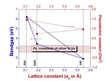
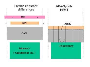
6 Issues With Mazimizing Al Mole Fraction in Alx Ga 1-x N AlN G Eg Al x Ga 1-x N GaN Lattice Constant InN GaN Pseudomorphic Relaxed with Misfit Morphology Mediated By Dislocaton x Al = 0.2 x Al = 0.4 x Al = 0.6 x HC = nm 250 nm 250 nm relaxed DISLOCATIONS LEAD TO PREMATURE RELAXATION OF AlGaN AND A POTENTIAL RELIABILITY PROBLEM BECAUSE OF THE METALLIZED PITS

![300Κ [cm 2 / Vs] 25 20 15 10 5 0 x = 0.09 0 10 100 1000 1000/T, 1/K Mobility v.](/docs-images/78/77649578/images/7-1.jpg "Al Fraction Plot 1500 1400 1300 1200 1100 1000 0 Relaxed 0.0 0.2 0.4 0.6 x Al 1.8 1.6 1.")

7 Issues With Increasing Mobility 30 INCREASING Al MOLE FRACTION DECREASES MOBILITY High Mobility AlGaN/GaN Structures Grown by RF Plasma Assisted MBE N S, cm -2 µ 300Κ [cm 2 / Vs] x = /T, 1/K Mobility v. Al Fraction Plot Relaxed x Al n s [10 13 cm -2 ] µ, cm 2 /Vs µ 300Κ [cm2 / Vs] Al 0.3 Ga 0.7 N R MS [nm]
8 Minimizing Gate Length Extension ELECTRONS IN SURFACE STATES AND/OR BUFFER TRAPS DEPLETE THE CHANNEL CAUSING GATE LENGTH EXTENSION I d (5 ma) DC Dispersion AC Load line SEVERE CONSEQUENCE: DISPERSION BETWEEN SMALL SIGNAL AND LARGE SIGNAL BEHAVIOR BECAUSE OF THE LARGE TRAP TIME CONSTANTS V ds (V) WHY DO THESE TRAPS ARISE?
9 Example of Advantage of WBG Devices 10-x power density ( > 10 W/mm) I N GaAs High Power Amplifier Module O U T 10-x reduction in power-combining Improved efficiency (> 60 %) Improved reliability Compact size Superior Performance at reduced cost I O N U T Equivalent High Power GaN Amplifier Module
10 Application Space Watts Ship Radar Airborne Radar Military Commercial Base THAAD Navy Decoy Decoy Station Shipboard Radar,DD21 LONGBOW Satcom Satcom Base Station MMDS, UNII VSAT Driver WLL Hiperlan LMDS MVDS Amp 3G Digital Radio BAT P31 Missile Seekers CAR S C X Ku K Ka Q V W 2 GHz 10 GHz 30 GHz 60 GHz Frequency Band
11 Schematic of Device Structure SiN Passivation SOURCE GATE DRAIN AlGaN 2DEG GaN Substrate: Typically Sapphire or SiC Nucleation Layer GaN, AlGaN or AlN
12 Ball and Stick Diagram of the GaN Crystal
13 Polarization World
14 How does the electron gas form in AlGaN/GaN structures? - A Q, AlGaN π Q, AlGaN π Al x Ga 1-x N GaN Q, GaN π P( x) = ( Qπ, AlGaN ) + ( Qπ, GaN ) Qπ, GaN Q π includes the contribution of spontaneous and piezo-electric contributions
15 How does the electron gas form in AlGaN/GaN structures? - B Q, InGaN π + Q, InGaN π In x Ga 1-x N ( π, GaN ) ( π InGaN ) P = Q + Q ( x), Q, GaN π Qπ, GaN Q π includes the contribution of spontaneous and piezo-electric contributions
16 How does the electron gas form in AlGaN/GaN structures? - C VAGaN l! EgGaN, + Ev= Maximum Dipole Moment AlGaN GaN Eg, GaN E v p s Q 2 π ( cm ) Q 2 π ( cm ) n s
17 How does the electron gas form in AlGaN/GaN structures? - D E DD AlGaN GaN E F Q ( cm ) N + 2 DD π Q π n s
 Dispersion AC Load line V ds")
18 Dispersion in AlGaN/Ga HEMTs DC I d (5 ma) Dispersion AC Load line V ds (V)
19 Source Lg GATE Electrons in Surface States AlGaN Drain GaN Depletion of 2DEG caused by occupied surface states

20 Performance of Passivated AlGaN/GaN HEMT on Sapphire
21 Performance of AlGaN/GaN HEMT on SiC (CLC) P out (db), Gain(dB), PAE (%) f=8ghz, Tuned for Power Pout Gain PAE Id P out = 10.3 W/mm PAE= 42% 41.6% I d (ma) P in (db)
22 Drain Bias Dependence of Rf Power (CLC) 10 PAE; P out f=8ghz P out (W/mm) PAE (%) Increasing V ds P in (db)

23 Flip-chip AlGaN/GaN HEMT for Thermal Management
 V ds")
24 I-V Curves from 8mm-wide HEMT V g start: +2V, Step: -2 V I d (A/divsion) V ds (V/divsion)
25 Low Flip-chip Wide Bandwidth Amplifier
26 Pulse Power Performance of mm-flipped Device Gain (db), DE(%), PAE(%) Gain DE PAE Pout P out (dbm) P in (dbm)
27 Power Performance vs. Year Cree 108W, CW Cree Power density (W/mm) 11 Power density Early Players Year Cornell UCSB CREE Cree UCSB HRL Cornell SiC Sapphire 60 Cree 50 Total power (W) Total power SiC Sapphire Early Players Cornell UCSB Year Includes ALL LEADING players in the field CREE CREE = Cree Lighting+ Cree-Durham Cree CREE HRL Cree NEC
28 Part II High Voltage Operation (> 330 V) of AlGaN/GaN HBTs
29 UCSB Bipolar transistor key issues Injection γ!1 n! 1 [I=I 0 exp (qv/nkt)] Emitter Base Transport -- α! 1 Collector Subcollector Collection C bc! 0 Output Conductance v! v sat [2 x 10 7 cm/s] (Kolnik et. al.) I C / V CE! 0 V br! E crit W C [E crit ~ 2 MV/cm] (Bhapkar and Shur.) ( W B / V CE! 0)
30 Hurdles with GaN bipolar transistors Lack of low damage etch to reveal base Leaky E/B junction Bad base contact No etch stop High R B Poor p-gan base contact Low p-gan base conductivity Deep acceptor (~160 mev) Hard to control junction placement in MOCVD due to memory effect of p-p dopant Mg Emitter Low minority carrier lifetime Surface leakage due to etch damage Base Collector Subcollector Dislocation causes leakage
31 UCSB Demonstration of dislocation enhanced leakage LEO used to investigate leakage of devices without dislocations. (Lee McCarthy et al.) AFM scan of wing vs Window on LEO GaN Leakage Current [A] Dislocated LEO Applied Bias [V] Leakage from Collector to Emitter, Wing vs Window Results: LEO device demonstrated Reduction in Leakage Stable operation past 20V Gain unchanged Devices on dislocated material also functional Regrowth Mask LEO GaN Regrowth Mask Standard template Explanation Thick substrate sufficiently reduces dislocations to prevent C/E short in window region Gain (τ e ) not currently limited by dislocation density
 Doping vs. Depth (010704GA, 8 µm collector) 1.E+17 Doping (cm -3 ) 1.E+16 1.E+15 1.")
32 UCSB Strategy: Thick Collector Decent dislocation density High quality MOCVD templates achieved Dislocation density ~ 5e8 cm -2 Low background doping N D < 1e16 cm -3 (Assuming uniform doping N D and E critical = 2 MV/cm, requires 10 µm to achieve 1 KV breakdown voltage.) Doping vs. Depth (010704GA, 8 µm collector) 1.E+17 Doping (cm -3 ) 1.E+16 1.E+15 1.E Depth (µm)

33 UCSB Emitter Regrowth Process Flow Selectively grow MOCVD emitter on base-collector structures. 1. Pattern regrowth mask 2. Regrow emitter layer by MOCVD 3. Remove mask and contact base and etch to collector 4. Contact collector, emitter Mask p Base n - Collector n + Subcollector Sapphire Substrate n + Emitter p Base n - Collector n + Subcollector Sapphire Substrate Regrown emitter n + Pd/Au Emitter p Base n - Collector Al/Au Al/Au n + Emitter p Base n - Collector n + Subcollector Sapphire Substrate n + Subcollector Sapphire Substrate
34 UCSB SIMS: Mg by MOCVD Severe memory effect observed in non-interrupted MOCVD growth Slow decay tail into GaN:Si regrown on as-grown GaN:Mg layer Concentration (cm -3 ) 1E+21 1E+20 1E+19 1E+18 1E+17 1E+16 1E+15 Turnoff of Mg source Decay rate ~ 140 nm/decade Si Mg Low Mg background in clean reactor Growth direction 230 nm 400 nm Depth (µm) Concentration (cm -3 ) 1.E+21 1.E+20 1.E+19 1.E+18 1.E+17 1.E+16 Regrown surface Decay rate ~ 115 nm/decade Si ~ 30 nm/decade Mg Depth (µm) Memory effect Slow decay tail in regrowth
35 UCSB SIMS: regrowth with surface treatment Regrown in Mg-free reactor and all grown by MOCVD Presence of an excessive amount of Mg on the surface, which can be removed by acid etch Occurrence of Mg diffusion, ~ 40 nm/decade sharpness achieved Mg concentration (a.u.) 1E+23 1E+22 1E+21 1E+20 1E+19 1E+18 1E+17 1E+16 1E+15 C D E Regrowth surface Depth (nm) C: as grown, ~100 nm/decade D: etch in HFand HCl for 5 min, ~ 50 nm/decade E: etch in BHF (1:20) for 15 sec and HCl for 20 sec, ~40 nm/decade Detection limit
36 UCSB Selectively regrown n/p diodes Mask enhanced growth complicates the analysis Regrowth rate depends on the mask layout, diode size etc Bunny ear regrowth profile is often seen Only the emitter edge is active in device operation due to highly resistive base layer The junction quality depends on how the regrowth is initiated, e.g. Temp, P, flows, presence of Si and Al etc. Bunny ear regrowth profile of two different square diodes
37
38 UCSB Regrown n/p Diodes Characteristics Comparison of various structures regrown on 0.5 µm GaN:Mg Run # Layer structure Growth Parameter G.R. Temp/Press (nm/min) (C/Torr) GF 400 nm GaN:Si (4e18 cm -3 ) ~ / AE AF GC 250 nm Al 0.06 GaN:Si (1e18) x Al ~ 5% 250 nm AlGaN:Si (1e18) 75 nm GaN->AlGaN:Si (1e18) 450 nm GaN:Si (1e18) 30 nm GaN ~30 ~30 ~ / / /300 I density (A/cm 2 ) x10-4 1x GF AE AF GC AA Year 2000 Year AA x Al ~ 5% 30 nm GaN:Si 30 nm AlGaN->GaN:Si 730 nm AlGaN:Si 60 nm GaN->AlGaN 60 nm GaN ~ / V (Volts)

39 UCSB HBT with 8 mm GaN collector Current gain (β) > 20 Common emitter operation > 300 V Non-passivated Base thickness 1000 Å Al 0.05 GaN emitter Vbr ~330 V
40 UCSB Device structure Utilization of uid GaN spacer and grading layer - HBTs with high emitter injection coefficiency Etch damage and current mask layout limits V br 4 nm GaN:Si (1e18 cm -3 ) contact 4 nm Al 0.05 GaN->GaN:Si (1e18 cm -3 ) grading 105 nm Al 0.05 GaN:Si (1e18 cm -3 ) emitter 8 nm GaN->Al 0.05 GaN (?3e18 cm -3 ) grading 8 nm uid GaN spacer 100 nm GaN:Mg (2e19 cm -3 ) base 8 µm uid GaN (4e15 cm -3 ) collector 2 µm GaN:Si (1e18 cm -3 ) subcollector Sapphire Effective collector thickness ~ 2-3 µm n + Subcollector n + Emitter 1000 Å p Base 8 µm n- collector Sapphire Substrate
41 UCSB I-V Characteristics reasonable base contacts Improved B/E diodes Rectifying B/C diodes, Vbr > 300 V 0.12 I (µa) V (Volts) I (ma) V BE (V) Base-emitter diode Base-collector diode
42 Summary Conclusion In selective emitter regrowth, a sharp Mg profile, ~ 40 nm/decade, enables the precise junction placement Improvement of regrown-emitter/base diodes Demonstration of high Vbr (> 300 V) with high β (DC common emitter operation up to 35)
AlGaN/GaN HEMTs and HBTs
 AlGaN/GaN HEMTs and HBTs Umesh K. Mishra PART I AlGaN/GaN HEMTs Materials Properties Comparison Material µ ε Eg BFOM JFM Tmax Ratio Ratio Si 1300 11.4 1.1 1.0 1.0 300 C GaAs 5000 13.1 1.4 9.6 3.5 300 C
International Workshop on Nitride Semiconductors (IWN 2016)
") International Workshop on Nitride Semiconductors (IWN 2016) Sheng Jiang The University of Sheffield Introduction The 2016 International Workshop on Nitride Semiconductors (IWN 2016) conference is held
International Workshop on Nitride Semiconductors (IWN 2016) Sheng Jiang The University of Sheffield Introduction The 2016 International Workshop on Nitride Semiconductors (IWN 2016) conference is held
Semiconductor Materials for Power Electronics (SEMPEL) GaN power electronics materials
 GaN power electronics materials") Semiconductor Materials for Power Electronics (SEMPEL) GaN power electronics materials Kjeld Pedersen Department of Physics and Nanotechnology, AAU SEMPEL Semiconductor Materials for Power Electronics
Semiconductor Materials for Power Electronics (SEMPEL) GaN power electronics materials Kjeld Pedersen Department of Physics and Nanotechnology, AAU SEMPEL Semiconductor Materials for Power Electronics
GaN MMIC PAs for MMW Applicaitons
 GaN MMIC PAs for MMW Applicaitons Miroslav Micovic HRL Laboratories LLC, 311 Malibu Canyon Road, Malibu, CA 9265, U. S. A. mmicovic@hrl.com Motivation for High Frequency Power sources 6 GHz 11 GHz Frequency
Department of Electrical Engineering IIT Madras
 Department of Electrical Engineering IIT Madras Sample Questions on Semiconductor Devices EE3 applicants who are interested to pursue their research in microelectronics devices area (fabrication and/or
Gallium Nitride & Related Wide Bandgap Materials and Devices
 Gallium Nitride & Related Wide Bandgap Materials and Devices Dr. Edgar J. Martinez Program Manager DARPATech 2000 GaAs IC Markets 1999 Market $11 Billion 2005 Market $20 Billion Consumers 2% Computers
Gallium nitride (GaN)
") 80 Technology focus: GaN power electronics Vertical, CMOS and dual-gate approaches to gallium nitride power electronics US research company HRL Laboratories has published a number of papers concerning
80 Technology focus: GaN power electronics Vertical, CMOS and dual-gate approaches to gallium nitride power electronics US research company HRL Laboratories has published a number of papers concerning
Ph.D. Defense. Broadband Power Amplifier
 Ph.D. Defense GaN HEMTs based Flip-chip Integrated Broadband Power Amplifier Jane Xu University of California at Santa Barbara Committee: Prof. Stephen Long Prof. Umesh Mishra Dr. Yi-feng Wu Prof. Bob
PROCESS DEVELOPMENT FOR SMALL-AREA GaN/AlGaN HBT s
 PROCESS DEVELOPMENT FOR SMALL-AREA GaN/AlGaN HBT s K.P.Lee (1), A.P.Zhang (1), G.Dang (1), F.Ren (1), J.Han (2), W.S.Hobson (3), J.Lopata (3), C.R.Abernathy (1), S.J.Pearton (1), J.W.Lee (4) (1) University
GaN HBT: Toward an RF Device
 IEEE TRANSACTIONS ON ELECTRON DEVICES, VOL. 48, NO. 3, MARCH 2001 543 GaN HBT: Toward an RF Device Lee S. McCarthy, Ioulia P. Smorchkova, Huili Xing, P. Kozodoy, Paul Fini, J. Limb, David L. Pulfrey, Fellow,
GaN: Applications: Optoelectronics
 GaN: Applications: Optoelectronics GaN: Applications: Optoelectronics - The GaN LED industry is >10 billion $ today. - Other optoelectronic applications of GaN include blue lasers and UV emitters and detectors.
GaN power electronics
 GaN power electronics The MIT Faculty has made this article openly available. Please share how this access benefits you. Your story matters. Citation As Published Publisher Lu, Bin, Daniel Piedra, and
Customized probe card for on-wafer testing of AlGaN/GaN power transistors
 Customized probe card for on-wafer testing of AlGaN/GaN power transistors R. Venegas 1, K. Armendariz 2, N. Ronchi 1 1 imec, 2 Celadon Systems Inc. Outline Introduction GaN for power switching applications
Sub 300 nm Wavelength III-Nitride Tunnel-Injected Ultraviolet LEDs
 Sub 300 nm Wavelength III-Nitride Tunnel-Injected Ultraviolet LEDs Yuewei Zhang, Sriram Krishnamoorthy, Fatih Akyol, Sadia Monika Siddharth Rajan ECE, The Ohio State University Andrew Allerman, Michael
Chapter 6. Silicon-Germanium Technologies
 Chapter 6 licon-germanium Technologies 6.0 Introduction The design of bipolar transistors requires trade-offs between a number of parameters. To achieve a fast base transit time, hence achieving a high
Customized probe card for on wafer testing of AlGaN/GaN power transistors
 Customized probe card for on wafer testing of AlGaN/GaN power transistors R. Venegas 1, K. Armendariz 2, N. Ronchi 1 1 imec, 2 Celadon Systems Inc. Presented by Bryan Root 2 Outline Introduction GaN for
AlGaN Polarization Graded Field Effect Transistors for High Linearity Microwave Applications
 AlGaN Polarization Graded Field Effect Transistors for High Linearity Microwave Applications Shahadat H. Sohel, Hao Xue, Towhidur Razzak, Sanyam Bajaj, Yuewei Zhang, Wu Lu, Siddharth Rajan Department of
Chapter 1. Introduction
 Chapter 1 Introduction 1.1 Introduction of Device Technology Digital wireless communication system has become more and more popular in recent years due to its capability for both voice and data communication.
From Bulk Gallium Nitride Material to Vertical GaN Devices
 From Bulk Gallium Nitride Material to Vertical GaN Devices Thomas Mikolajick 1,2, Stefan Schmult 2, Rico Hentschel 1, Patrick Hofmann 1, and Andre Wachowiak 1 1 NaMLab ggmbh 2 Chair of Nanoelectronic Materials,
MSE 410/ECE 340: Electrical Properties of Materials Fall 2016 Micron School of Materials Science and Engineering Boise State University
 MSE 410/ECE 340: Electrical Properties of Materials Fall 2016 Micron School of Materials Science and Engineering Boise State University Practice Final Exam 1 Read the questions carefully Label all figures
Development of Gallium Nitride High Electron Mobility Transistors for Cellular Base Stations
 ELECTRONICS Development of Gallium Nitride High Electron Mobility Transistors for Cellular Base Stations Kazutaka INOUE*, Seigo SANO, Yasunori TATENO, Fumikazu YAMAKI, Kaname EBIHARA, Norihiko UI, Akihiro
Advance Datasheet Revision: October Applications
 APN149 Applications Military SatCom Phased-Array Radar Applications Point-to-Point Radio Point-to-Multipoint Communications Terminal Amplifiers Product Description X = 4.4mm Y = 2.28mm Product Features
High Power Wideband AlGaN/GaN HEMT Feedback. Amplifier Module with Drain and Feedback Loop. Inductances
 High Power Wideband AlGaN/GaN HEMT Feedback Amplifier Module with Drain and Feedback Loop Inductances Y. Chung, S. Cai, W. Lee, Y. Lin, C. P. Wen, Fellow, IEEE, K. L. Wang, Fellow, IEEE, and T. Itoh, Fellow,
III-Nitride microwave switches Grigory Simin
 Microwave Microelectronics Laboratory Department of Electrical Engineering, USC Research Focus: - Wide Bandgap Microwave Power Devices and Integrated Circuits - Physics, Simulation, Design and Characterization
Wide Band-Gap Power Device
 Wide Band-Gap Power Device 1 Contents Revisit silicon power MOSFETs Silicon limitation Silicon solution Wide Band-Gap material Characteristic of SiC Power Device Characteristic of GaN Power Device 2 1
Innovative Technologies for RF & Power Applications
 Innovative Technologies for RF & Power Applications > Munich > Nov 14, 2017 1 Key Technologies Key Technologies Veeco Market Focus Advanced Packaging, MEMS & RF Lighting, Display & Power Electronics Lithography
Insulated Gate Bipolar Transistor (IGBT)
") nsulated Gate Bipolar Transistor (GBT) Comparison between BJT and MOS power devices: BJT MOS pros cons pros cons low V O thermal instability thermal stability high R O at V MAX > 400 V high C current complex
nsulated Gate Bipolar Transistor (GBT) Comparison between BJT and MOS power devices: BJT MOS pros cons pros cons low V O thermal instability thermal stability high R O at V MAX > 400 V high C current complex
Novel III-Nitride HEMTs
 IEEE EDS Distinguished Lecture Boston Chapter, July 6 2005 Novel III-Nitride HEMTs Professor Kei May Lau Department of Electrical and Electronic Engineering Hong Kong University of Science and Technology
N-polar GaN/ AlGaN/ GaN high electron mobility transistors
 JOURNAL OF APPLIED PHYSICS 102, 044501 2007 N-polar GaN/ AlGaN/ GaN high electron mobility transistors Siddharth Rajan a Electrical and Computer Engineering Department, University of California, Santa
Gallium nitride futures and other stories
 Dr Mike Cooke Gallium nitride-based devices look set to have increasingly wide application, at least if the contributions at December s International Electron Devices Meeting () in Washington DC are anything
GaN/SiC Bare Die Power HEMT DC-15 GHz
 GaN/SiC Bare Die Power HEMT DC-15 GHz DESCRIPTION AMCOM s is a discrete GaN/SiC HEMT that has a total gate width of mm (Eight 1.mm FETs in parallel). It is a bare die which can be operated up to 15 GHz.
NAME: Last First Signature
 UNIVERSITY OF CALIFORNIA, BERKELEY College of Engineering Department of Electrical Engineering and Computer Sciences EE 130: IC Devices Spring 2003 FINAL EXAMINATION NAME: Last First Signature STUDENT
RF and Microwave Semiconductor Technologies
 RF and Microwave Semiconductor Technologies Muhammad Fahim Ul Haque, Department of Electrical Engineering, Linköping University muhha@isy.liu.se Note: 1. This presentation is for the course of State of
Wideband Reconfigurable Harmonically Tuned GaN SSPA for Cognitive Radios
 The University Of Cincinnati College of Engineering Wideband Reconfigurable Harmonically Tuned GaN SSPA for Cognitive Radios Seth W. Waldstein The University of Cincinnati-Main Campus Miguel A. Barbosa
Simulation of GaAs MESFET and HEMT Devices for RF Applications
 olume, Issue, January February 03 ISSN 78-6856 Simulation of GaAs MESFET and HEMT Devices for RF Applications Dr.E.N.GANESH Prof, ECE DEPT. Rajalakshmi Institute of Technology ABSTRACT: Field effect transistor
Advance Datasheet Revision: May 2013
 Applications Military SatCom Phased-Array Radar Applications Point-to-Point Radio Point-to-Multipoint Communications Terminal Amplifiers X = 4.4mm Y = 2.28mm Product Features RF frequency: 18 to 23 GHz
Record Extrinsic Transconductance (2.45 ms/μm at V DS = 0.5 V) InAs/In 0.53 Ga 0.47 As Channel MOSFETs Using MOCVD Source-Drain Regrowth
 InAs/In 0.53 Ga 0.47 As Channel MOSFETs Using MOCVD Source-Drain Regrowth") Record Extrinsic Transconductance (2.45 ms/μm at = 0.5 V) InAs/In 0.53 Ga 7 As Channel MOSFETs Using MOCVD Source-Drain Regrowth Sanghoon Lee 1*, C.-Y. Huang 1, A. D. Carter 1, D. C. Elias 1, J. J. M.
Record Extrinsic Transconductance (2.45 ms/μm at = 0.5 V) InAs/In 0.53 Ga 7 As Channel MOSFETs Using MOCVD Source-Drain Regrowth Sanghoon Lee 1*, C.-Y. Huang 1, A. D. Carter 1, D. C. Elias 1, J. J. M.
Indium Phosphide and Related Materials Selectively implanted subcollector DHBTs
 Indium Phosphide and Related Materials - 2006 Selectively implanted subcollector DHBTs Navin Parthasarathy, Z. Griffith, C. Kadow, U. Singisetti, and M.J.W. Rodwell Dept. of Electrical and Computer Engineering,
Composants HEMT InAlGaN/GaN pour applications en bandes Ka et Q.
 Composants HEMT InAlGaN/GaN pour applications en bandes Ka et Q. Stéphane PIOTROWICZ, Olivier PATARD, Jean-Claude JACQUET, Piero GAMARRA, Christian DUA & Sylvain DELAGE RF & Microwave 22 mars 2018 Copyright
Fundamentals of Power Semiconductor Devices
 В. Jayant Baliga Fundamentals of Power Semiconductor Devices 4y Spri ringer Contents Preface vii Chapter 1 Introduction 1 1.1 Ideal and Typical Power Switching Waveforms 3 1.2 Ideal and Typical Power Device
600V GaN Power Transistor
 600V GaN Power Transistor Sample Available Features Normally-Off Current-Collapse-Free Zero Recovery GaN Power Transistor (TO220 Package) ID(Continuous) : 15A RDS(on) : 65m Qg : 11nC Applications Power
Final Report. Contract Number Title of Research Principal Investigator
 Final Report Contract Number Title of Research Principal Investigator Organization N00014-05-1-0135 AIGaN/GaN HEMTs on semi-insulating GaN substrates by MOCVD and MBE Dr Umesh Mishra University of California,
Power Semiconductor Devices
 TRADEMARK OF INNOVATION Power Semiconductor Devices Introduction This technical article is dedicated to the review of the following power electronics devices which act as solid-state switches in the circuits.
CHAPTER 2 HEMT DEVICES AND BACKGROUND
 CHAPTER 2 HEMT DEVICES AND BACKGROUND 2.1 Overview While the most widespread application of GaN-based devices is in the fabrication of blue and UV LEDs, the fabrication of microwave power devices has attracted
EJERCICIOS DE COMPONENTES ELECTRÓNICOS. 1 er cuatrimestre
 EJECICIOS DE COMPONENTES ELECTÓNICOS. 1 er cuatrimestre 2 o Ingeniería Electrónica Industrial Juan Antonio Jiménez Tejada Índice 1. Basic concepts of Electronics 1 2. Passive components 1 3. Semiconductors.
Advance Datasheet Revision: April 2015
 APN 1-1 GHz Advance Datasheet Revision: April Applications Point-to-Point Digital Radios Point-to-Multipoint Digital Radios VSAT Test Instrumentation X = 3 um Y = 3 um Product Features RF frequency: 1
GaN/SiC Bare Die Power HEMT DC-15 GHz
 GaN/SiC Bare Die Power HEMT DC-15 GHz DESCRIPTION AMCOM s is a discrete GaN/SiC HEMT that has a total gate width of 5mm (Four 1.mm FETs in parallel). It is a bare die which can be operated up to 15 GHz.
100+ GHz Transistor Electronics: Present and Projected Capabilities
 21 IEEE International Topical Meeting on Microwave Photonics, October 5-6, 21, Montreal 1+ GHz Transistor Electronics: Present and Projected Capabilities Mark Rodwell University of California, Santa Barbara
Monolithic integration of GaN power transistors integrated with gate drivers
 October 3-5, 2016 International Workshop on Power Supply On Chip (PwrSoC 2016) Monolithic integration of GaN power transistors integrated with gate drivers October 4, 2016 Tatsuo Morita Automotive & Industrial
Bipolar Junction Transistors (BJT)
") Bipolar Junction Transistors (BJT) deal Transistor Bipolar Transistor Terminals P Bipolar Transistor Physics Large Signal Model Early Effect Small Signal Model Reading: (Sedra, Smith, 7 th edition) 4.1
Bipolar Junction Transistors (BJT) deal Transistor Bipolar Transistor Terminals P Bipolar Transistor Physics Large Signal Model Early Effect Small Signal Model Reading: (Sedra, Smith, 7 th edition) 4.1
6.012 Microelectronic Devices and Circuits
 Page 1 of 13 YOUR NAME Department of Electrical Engineering and Computer Science Massachusetts Institute of Technology 6.012 Microelectronic Devices and Circuits Final Eam Closed Book: Formula sheet provided;
100nm GaN on Si: A Pioneering Technology to Enable High RF Power in Millimeter Wave Bands NEW ENGLAND IMAPS SYMPOSIUM MAY 5, 2015
 Innovating with III-V s 100nm GaN on Si: A Pioneering Technology to Enable High RF Power in Millimeter Wave Bands NEW ENGLAND IMAPS SYMPOSIUM MAY 5, 2015 By Dr Fabien ROBERT Sales & Application Team Manager,
MECGaNC30. 4 to 6 GHz GaN HEMT Power Amplifier. Main Features. Product Description. Applications
 Main Features 0.25µm GaN HEMT Technology 4.1 5.9 GHz full performances Frequency Range W Output Power @ Pin 27.5 dbm 37% PAE @ Pin 27.5 dbm % PAE @ Pout Watt 27 db Small Signal Gain Product Description
= 25 C) Parameter 0.5 GHz 1.0 GHz 2.5 GHz 4.0 GHz 6.0 GHz Units. Gain db. 23 dbm W
 Parameter 0.5 GHz 1.0 GHz 2.5 GHz 4.0 GHz 6.0 GHz Units. Gain db. 23 dbm W") CMPA6D Watt, MHz - 6 MHz GaN HEMT MMIC Power Amplifier Cree s CMPA6D is a gallium nitride (GaN) High Electron Mobility Transistor (HEMT) based monolithic microwave integrated circuit (MMIC). GaN has superior
CMPA6D Watt, MHz - 6 MHz GaN HEMT MMIC Power Amplifier Cree s CMPA6D is a gallium nitride (GaN) High Electron Mobility Transistor (HEMT) based monolithic microwave integrated circuit (MMIC). GaN has superior
= 25 C) Parameter 1.0 GHz 2.0 GHz 3.0 GHz 4.0 GHz 5.0 GHz 6.0 GHz Units. Gain db. 32 dbm W
 Parameter 1.0 GHz 2.0 GHz 3.0 GHz 4.0 GHz 5.0 GHz 6.0 GHz Units. Gain db. 32 dbm W") CMPA006005D 5 W, 0 MHz - 6.0 GHz, GaN MMIC, Power Amplifier Cree s CMPA006005D is a gallium nitride (GaN) High Electron Mobility Transistor (HEMT) based monolithic microwave integrated circuit (MMIC).
CMPA006005D 5 W, 0 MHz - 6.0 GHz, GaN MMIC, Power Amplifier Cree s CMPA006005D is a gallium nitride (GaN) High Electron Mobility Transistor (HEMT) based monolithic microwave integrated circuit (MMIC).
Section 2.3 Bipolar junction transistors - BJTs
 Section 2.3 Bipolar junction transistors - BJTs Single junction devices, such as p-n and Schottkty diodes can be used to obtain rectifying I-V characteristics, and to form electronic switching circuits
A new Vertical JFET Technology for Harsh Radiation Applications
 A New Vertical JFET Technology for Harsh Radiation Applications ISPS 2016 1 A new Vertical JFET Technology for Harsh Radiation Applications A Rad-Hard switch for the ATLAS Inner Tracker P. Fernández-Martínez,
PRELIMINARY = 25 C) Parameter GHz 14.0 GHz 14.5 GHz Units Small Signal Gain db P SAT. = 26 dbm W P 3dB
 Parameter GHz 14.0 GHz 14.5 GHz Units Small Signal Gain db P SAT. = 26 dbm W P 3dB") CMPADE030D PRELIMINARY 30 W, 3.75-4.5 GHz, 40 V, GaN MMIC, Power Amplifier Cree s CMPADE030D is a gallium nitride (GaN) High Electron Mobility Transistor (HEMT) based monolithic microwave integrated circuit
CMPADE030D PRELIMINARY 30 W, 3.75-4.5 GHz, 40 V, GaN MMIC, Power Amplifier Cree s CMPADE030D is a gallium nitride (GaN) High Electron Mobility Transistor (HEMT) based monolithic microwave integrated circuit
Microwave & RF 22 nd of March 2018 D. FLORIOT
 Microwave & RF 22 nd of March 2018 D. FLORIOT Outine Introduction GaN technology roadmap GH15-10 : Up to Ka band GH10 : Towards high frequency (Q / V bands) GaN : Technology & Integration 2 UMS at a glance
Record I on (0.50 ma/μm at V DD = 0.5 V and I off = 100 na/μm) 25 nm-gate-length ZrO 2 /InAs/InAlAs MOSFETs
 25 nm-gate-length ZrO 2 /InAs/InAlAs MOSFETs") Record I on (0.50 ma/μm at V DD = 0.5 V and I off = 100 na/μm) 25 nm-gate-length ZrO 2 /InAs/InAlAs MOSFETs Sanghoon Lee 1*, V. Chobpattana 2,C.-Y. Huang 1, B. J. Thibeault 1, W. Mitchell 1, S. Stemmer
Record I on (0.50 ma/μm at V DD = 0.5 V and I off = 100 na/μm) 25 nm-gate-length ZrO 2 /InAs/InAlAs MOSFETs Sanghoon Lee 1*, V. Chobpattana 2,C.-Y. Huang 1, B. J. Thibeault 1, W. Mitchell 1, S. Stemmer
Reg. No. : Question Paper Code : B.E./B.Tech. DEGREE EXAMINATION, NOVEMBER/DECEMBER Second Semester
 WK 5 Reg. No. : Question Paper Code : 27184 B.E./B.Tech. DEGREE EXAMINATION, NOVEMBER/DECEMBER 2015. Time : Three hours Second Semester Electronics and Communication Engineering EC 6201 ELECTRONIC DEVICES
Power Semiconductor Devices - Silicon vs. New Materials. Si Power Devices The Dominant Solution Today
 Power Semiconductor Devices - Silicon vs. New Materials Jim Plummer Stanford University IEEE Compel Conference July 10, 2017 Market Opportunities for Power Devices Materials Advantages of SiC and GaN vs.
Preliminary Datasheet Revision: January 2016
 Preliminary Datasheet Revision: January 216 Applications Point-to-Point Digital Radios Point-to-Multipoint Digital Radios SATCOM Terminals X = 3.65mm Y = 2.3mm Product Features RF frequency: 27 to 31 GHz
= 25 C) Parameter 0.5 GHz 1.0 GHz 2.5 GHz 4.0 GHz 6.0 GHz Units. Gain db. 23 dbm W
 Parameter 0.5 GHz 1.0 GHz 2.5 GHz 4.0 GHz 6.0 GHz Units. Gain db. 23 dbm W") CMPA0060002D 2 Watt, MHz - 6000 MHz GaN HEMT MMIC Power Amplifier Cree s CMPA0060002D is a gallium nitride (GaN) High Electron Mobility Transistor (HEMT) based monolithic microwave integrated circuit (MMIC).
CMPA0060002D 2 Watt, MHz - 6000 MHz GaN HEMT MMIC Power Amplifier Cree s CMPA0060002D is a gallium nitride (GaN) High Electron Mobility Transistor (HEMT) based monolithic microwave integrated circuit (MMIC).
& ) > 35W, 33-37% PAE
 > 35W, 33-37% PAE") Outline Status of Linear and Nonlinear Modeling for GaN MMICs Presented at IMS11 June, 11 Walter R. Curtice, Ph. D. Consulting www.curtice.org State of the Art Modeling considerations, types of models,
Outline Status of Linear and Nonlinear Modeling for GaN MMICs Presented at IMS11 June, 11 Walter R. Curtice, Ph. D. Consulting www.curtice.org State of the Art Modeling considerations, types of models,
Development of Microwave and Terahertz Detectors Utilizing AlN/GaN High Electron Mobility Transistors
 Development of Microwave and Terahertz Detectors Utilizing AlN/GaN High Electron Mobility Transistors L. Liu 1, 2,*, B. Sensale-Rodriguez 1, Z. Zhang 1, T. Zimmermann 1, Y. Cao 1, D. Jena 1, P. Fay 1,
EE 5611 Introduction to Microelectronic Technologies Fall Thursday, September 04, 2014 Lecture 02
 EE 5611 Introduction to Microelectronic Technologies Fall 2014 Thursday, September 04, 2014 Lecture 02 1 Lecture Outline Review on semiconductor materials Review on microelectronic devices Example of microelectronic
4.2.2 Metal Oxide Semiconductor Field Effect Transistor (MOSFET)
") 4.2.2 Metal Oxide Semiconductor Field Effect Transistor (MOSFET) The Metal Oxide Semitonductor Field Effect Transistor (MOSFET) has two modes of operation, the depletion mode, and the enhancement mode.
4.2.2 Metal Oxide Semiconductor Field Effect Transistor (MOSFET) The Metal Oxide Semitonductor Field Effect Transistor (MOSFET) has two modes of operation, the depletion mode, and the enhancement mode.
InP HBT technology development at IEMN
 InP HBT technology development at IEMN Advanced NanOmetric Devices Group, Institut d Electronique de Microelectronique et de Nanotechnology, Lille, FRANCE Date Outline Which applications for THz GaAsSb/InP
Graded P-AlGaN Superlattice for Reduced Electron Leakage in Tunnel- Injected UVC LEDs
 Graded P-AlGaN Superlattice for Reduced Electron Leakage in Tunnel- Injected UVC LEDs Yuewei Zhang, Sriram Krishnamoorthy, Fatih Akyol, Zane Jamal-Eddine Siddharth Rajan ECE, The Ohio State University
Alternative Channel Materials for MOSFET Scaling Below 10nm
 Alternative Channel Materials for MOSFET Scaling Below 10nm Doug Barlage Electrical Requirements of Channel Mark Johnson Challenges With Material Synthesis Introduction Outline Challenges with scaling
Investigation of electrically-active defects in AlGaN/GaN high electron mobility
 Investigation of electrically-active defects in AlGaN/GaN high electron mobility transistors by spatially-resolved spectroscopic scanned probe techniques. Dissertation Presented in Partial Fulfillment
MECXQMM-60W. 8.3 to 10.3 GHz GaN HEMT Power Amplifier
 Pout (dbm), PAE(%) Functional Block Diagram Main Features 0.25µm GaN HEMT Technology 8.3 10.3 GHz full performances Frequency Range 60W Output Power @ Pin 40.5 dbm PAE > 33% @ Pin 40.5 dbm Linear Gain
INVESTIGATION OF DEGRADATION EFFECTS DUE TO GATE STRESS. IN GaN-ON-Si HIGH ELECTRON MOBILITY TRANSISTORS THROUGH ANALYSIS OF LOW FREQUENCY NOISE
 INVESTIGATION OF DEGRADATION EFFECTS DUE TO GATE STRESS IN GaN-ON-Si HIGH ELECTRON MOBILITY TRANSISTORS THROUGH ANALYSIS OF LOW FREQUENCY NOISE A Thesis presented to the Faculty of California Polytechnic
Electronics I - Physics of Bipolar Transistors
 Chapter 5 Electronics I - Physics of Bipolar Transistors B E N+ P N- C B E C Fall 2017 claudio talarico 1 source: Sedra & Smith Thin Base Types of Bipolar Transistors n+ p n- Figure - A simplified structure
E-MODE III-N HIGH-VOLTAGE TRANSISTOR DEVELOPMENT
 1 E-MODE III-N HIGH-VOLTAGE TRANSISTOR DEVELOPMENT 1 st -Year Final Project Report (Feb 2010 March 2011) Presented to Intersil Corp., Milpitas CA Program Manager: Dr. François Hébert Georgia Tech PIs:
CMPA1D1E025F. 25 W, GHz, 40 V, Ku-Band GaN MMIC, Power Amplifier. Typical Performance Over GHz (T C. Features.
 CMPA1D1E025F 25 W, 13.75-14.5 GHz, 40 V, Ku-Band GaN MMIC, Power Amplifier Cree s CMPA1D1E025F is a gallium nitride (GaN) High Electron Mobility Transistor (HEMT) based monolithic microwave integrated
DC Analysis of InP/GaAsSb DHBT Device Er. Ankit Sharma 1, Dr. Sukhwinder Singh 2
 IOSR Journal of Electronics and Communication Engineering (IOSR-JECE) e-issn: 2278-2834,p- ISSN: 2278-8735.Volume 10, Issue 5, Ver. I (Sep - Oct.2015), PP 48-52 www.iosrjournals.org DC Analysis of InP/GaAsSb
Investigations on Compound Semiconductor High Electron Mobility Transistor (HEMT)
") Investigations on Compound Semiconductor High Electron Mobility Transistor (HEMT) Nov. 26, 2004 Outline I. Introduction: Why needs high-frequency devices? Why uses compound semiconductors? How to enable
Investigations on Compound Semiconductor High Electron Mobility Transistor (HEMT) Nov. 26, 2004 Outline I. Introduction: Why needs high-frequency devices? Why uses compound semiconductors? How to enable
Electronics Review Flashcards
 November 21, 2011 1 Op Amps 2 Diodes 3 Silicon 4 pn Junctions 5 BJTs 6 MOSFETs Open Loop Characteristics Open-Loop Op-Amp Characteristics (first-order model) Closed Loop Characteristics Closed-Loop Op-Amp
Advance Datasheet Revision: January 2015
 Advance Datasheet Revision: January 215 Applications Military SatCom Phased-Array Radar Applications Terminal Amplifiers X = 3.7mm Y = 3.2mm Product Features RF frequency: 43 to 46 GHz Linear Gain: 2 db
Student Lecture by: Giangiacomo Groppi Joel Cassell Pierre Berthelot September 28 th 2004
 Student Lecture by: Giangiacomo Groppi Joel Cassell Pierre Berthelot September 28 th 2004 Lecture outline Historical introduction Semiconductor devices overview Bipolar Junction Transistor (BJT) Field
NPA105-D. Preliminary GHz GaN 40W Power Amplifier. Product Description: Key Features:
 Product Description: The Nxbeam is a Ku-band high power GaN MMIC fabricated in 0.2um GaN HEMT on SiC. This part is ideally suited for satellite communications, point-to-point radios, and radar applications.
GaN Transistors for Efficient Power Conversion
 GaN Transistors for Efficient Power Conversion Agenda How GaN works Electrical Characteristics Design Basics Design Examples Summary 2 2 How GaN Works 3 3 The Ideal Power Switch Block Infinite Voltage
30% PAE W-band InP Power Amplifiers using Sub-quarter-wavelength Baluns for Series-connected Power-combining
 2013 IEEE Compound Semiconductor IC Symposium, October 13-15, Monterey, C 30% PAE W-band InP Power Amplifiers using Sub-quarter-wavelength Baluns for Series-connected Power-combining 1 H.C. Park, 1 S.
techniques, and gold metalization in the fabrication of this device.
 Up to 6 GHz Medium Power Silicon Bipolar Transistor Chip Technical Data AT-42 Features High Output Power: 21. dbm Typical P 1 db at 2. GHz 2.5 dbm Typical P 1 db at 4. GHz High Gain at 1 db Compression:
Defense Technical Information Center Compilation Part Notice
 UNCLASSIFIED Defense Technical Information Center Compilation Part Notice ADP015074 TITLE: Channel Recessed 4H-SiC MESFETs with Ft o f14.5ghz and F max of 40GHz DISTRIBUTION: Approved for public release,
Up to 6 GHz Low Noise Silicon Bipolar Transistor Chip. Technical Data AT-41400
 Up to 6 GHz Low Noise Silicon Bipolar Transistor Chip Technical Data AT-1 Features Low Noise Figure: 1.6 db Typical at 3. db Typical at. GHz High Associated Gain: 1.5 db Typical at 1.5 db Typical at. GHz
GaN electronics: what can epitaxy enable
 GaN electronics: what can epitaxy enable nmi meeting Integrating wide bandgap and high performance silicon semiconductors into systems Cranfield University: 22 nd Oct 2015 Trevor Martin FinstP, IQE Cardiff
= 25 C) Parameter 5.5 GHz 6.5 GHz 7.5 GHz 8.5 GHz Units Small Signal Gain db P OUT
 Parameter 5.5 GHz 6.5 GHz 7.5 GHz 8.5 GHz Units Small Signal Gain db P OUT") CMPA5585030D 30 W, 5.5-8.5 GHz, GaN MMIC, Power Amplifier Cree s CMPA5585030D is a gallium nitride (GaN) High Electron Mobility Transistor (HEMT) based monolithic microwave integrated circuit (MMIC). GaN
CMPA5585030D 30 W, 5.5-8.5 GHz, GaN MMIC, Power Amplifier Cree s CMPA5585030D is a gallium nitride (GaN) High Electron Mobility Transistor (HEMT) based monolithic microwave integrated circuit (MMIC). GaN
ATF High Intercept Low Noise Amplifier for the MHz PCS Band using the Enhancement Mode PHEMT
 ATF-54143 High Intercept Low Noise Amplifier for the 185 191 MHz PCS Band using the Enhancement Mode PHEMT Application Note 1222 Introduction Avago Technologies ATF-54143 is a low noise enhancement mode
= 25 C) Parameter 2.7 GHz 2.9 GHz 3.1 GHz 3.3 GHz 3.5 GHz Units Small Signal Gain db
 Parameter 2.7 GHz 2.9 GHz 3.1 GHz 3.3 GHz 3.5 GHz Units Small Signal Gain db") CMPA273575D 75 W, 2.7-3.5 GHz, GaN MMIC, Power Amplifier Cree s CMPA273575D is a gallium nitride (GaN) High Electron Mobility Transistor (HEMT) based monolithic microwave integrated circuit (MMIC). GaN
CMPA273575D 75 W, 2.7-3.5 GHz, GaN MMIC, Power Amplifier Cree s CMPA273575D is a gallium nitride (GaN) High Electron Mobility Transistor (HEMT) based monolithic microwave integrated circuit (MMIC). GaN
ATF Enhancement Mode [1] Pseudomorphic HEMT in SOT 89 Package
![ATF Enhancement Mode [1] Pseudomorphic HEMT in SOT 89 Package](/thumbs/86/93207835.jpg "ATF Enhancement Mode [1] Pseudomorphic HEMT in SOT 89 Package") ATF-3189 Enhancement Mode [1] Pseudomorphic HEMT in SOT 89 Package Data Sheet Description Avago Technologies s ATF-3189 is a single-voltage high linearity, low noise E-pHEMT FET packaged in a low cost
ATF-3189 Enhancement Mode [1] Pseudomorphic HEMT in SOT 89 Package Data Sheet Description Avago Technologies s ATF-3189 is a single-voltage high linearity, low noise E-pHEMT FET packaged in a low cost
Optical Fiber Communication Lecture 11 Detectors
 Optical Fiber Communication Lecture 11 Detectors Warriors of the Net Detector Technologies MSM (Metal Semiconductor Metal) PIN Layer Structure Semiinsulating GaAs Contact InGaAsP p 5x10 18 Absorption InGaAs
Physics of Bipolar Transistor
 Physics of Bipolar Transistor Motivations - In many electronic applications, amplifier is the most fundamental building block. Ex Audio amplifier: amplifies electric signal to drive a speaker RF Power
PERSPECTIVES FOR DISRUPTIVE 200MM/8-INCH GAN POWER DEVICE AND GAN-IC TECHNOLOGY DR. DENIS MARCON SR. BUSINESS DEVELOPMENT MANAGER
 PERSPECTIVES FOR DISRUPTIVE 200MM/8-INCH GAN POWER DEVICE AND GAN-IC TECHNOLOGY DR. DENIS MARCON SR. BUSINESS DEVELOPMENT MANAGER What I will show you today 200mm/8-inch GaN-on-Si e-mode/normally-off technology
ELECTRONIC DEVICES AND CIRCUITS
 ELECTRONIC DEVICES AND CIRCUITS 1. As compared to a full wave rectifier using 2 diodes, the four diode bridge rectifier has the dominant advantage of (a) Higher current carrying (b) lower peak inverse
= 25 C) Parameter 8.0 GHz 9.0 GHz 10.0 GHz 11.0 GHz Units Small Signal Gain db P OUT. = 25 dbm W Power P IN
 Parameter 8.0 GHz 9.0 GHz 10.0 GHz 11.0 GHz Units Small Signal Gain db P OUT. = 25 dbm W Power P IN") CMPA80B05D 5 W, 8.0 -.0 GHz, GaN MMIC, Power Amplifier Cree s CMP80B05D is a gallium nitride (GaN) High Electron Mobility Transistor (HEMT) based monolithic microwave integrated circuit (MMIC). GaN has
CMPA80B05D 5 W, 8.0 -.0 GHz, GaN MMIC, Power Amplifier Cree s CMP80B05D is a gallium nitride (GaN) High Electron Mobility Transistor (HEMT) based monolithic microwave integrated circuit (MMIC). GaN has
We are right on schedule for this deliverable. 4.1 Introduction:
 DELIVERABLE # 4: GaN Devices Faculty: Dipankar Saha, Subhabrata Dhar, Subhananda Chakrabati, J Vasi Researchers & Students: Sreenivas Subramanian, Tarakeshwar C. Patil, A. Mukherjee, A. Ghosh, Prantik
RADIATION RESPONSE AND RELIABILITY OF HIGH SPEED AlGaN/GaN HEMTS
 RADIATION RESPONSE AND RELIABILITY OF HIGH SPEED AlGaN/GaN HEMTS By Jin Chen Dissertation Submitted to the Faculty of the Graduate school of Vanderbilt University in partial fulfillment of the requirements