VCO Design Project ECE218B Winter 2011
|
|
|
- Tracey Fox
- 6 years ago
- Views:
Transcription
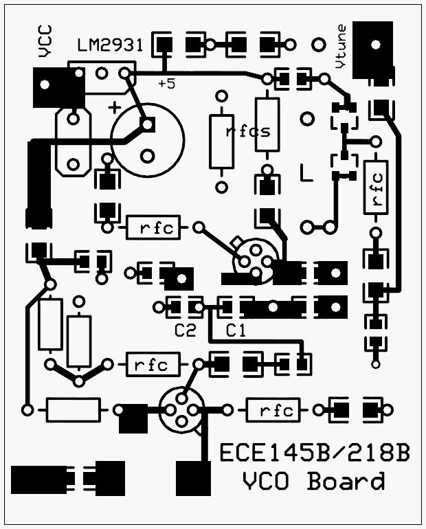
1 VCO Design Project ECE218B Winter 2011 Report due 2/18/2011 VCO DESIGN GOALS. Design, build, and test a voltage-controlled oscillator (VCO). 1. Design VCO for highest center frequency (< 400 MHz). 2. At least 10 MHz tuning range. In addition, you need to observe the following specs: Varactor tuning voltage range Supply voltage Output power Second and third harmonic 1 to 5 volts +6 V -3 to 0 dbm in 50 ohm load -25 dbc minimum 1. You will determine the oscillator type that you will design based upon achieving a center frequency as high as possible but below 400 MHz. You decide on either common gate/base or common drain/collector configuration. You can use either the J310 N- channel JFET or 2N5179 for the oscillator and the 2N5179 BJT for the buffer amp. Data sheets are on the course web page, and there are ADS models for these devices in the RF Transistor Library/Packaged BJTs (pb_mot_2n5179_ ) and Analog Parts Library (ap_njf_j310_ ). 2. The electrical tuning of the oscillator will make use of the BB131 varactor diode. Connect two of these diodes back-to-back for improved harmonic distortion. Refer to the data sheet on the course web page. The varactor Q is typically 150 at 200 MHz and 5 volts reverse bias. You should avoid biasing the varactor under 1 volt reverse bias so that the Q remains high. Isolate the bias port with an RF choke, series resistor (to De-Q the choke), R 1 to isolate C B from the tuning port, and bypass capacitor (choose value for series resonance at 135 MHz). The time constant of R 1 C B should be no larger than 10 S. Vtune R 1 R 2 RFC C B The varactor diode TC is shown on the data sheet roughly +250 ppm/ o C. This is an unacceptably high TC for the entire resonator, however, the varactor provides only a small part of the total capacitance. You should implement the fixed capacitors in the resonator with zero TC (NP0) capacitors. The inductor core material has a TC of 0 ppm/ o C.
2 Chip inductors are not recommended for the resonator because their unloaded Q is quite low, on the order of 20 to 30 at 200 MHz, therefore you will fabricate wirewound inductors on toroidal core material. The inductance of the toroidal inductor can be estimated by the equation below; use an A L = 3 for the type 0 material with OD. Typical unloaded Q at 200 MHz is on the order of 100 and is better when turns are bunched together. L( H) # turns 100 A L ( H / 100turns) Verify that your inductance is correct with the network analyzer to avoid needless frustration. The formula is only approximate. A cylindrical wire coil can also be used, but will be sensitive to bending and position and will also have a temperature coefficient. 3. Do a detailed hand analysis of your oscillator, predicting startup conditions and the oscillation amplitude. Do not use high bias current for your oscillator this is neither necessary nor desirable for good startup and stability and will increase power dissipation. Include the 5V voltage regulator to power your oscillator. The oscillator is intended to operate from a 6V battery, and you want the V CC to remain constant as the battery voltage drops. The hand analysis should be followed by ADS simulations before attempting to build the oscillator. A large-signal nonlinear analysis on the closed loop oscillator can be done by transient analysis or harmonic balance. Starting the oscillator in the transient simulator will require an impulse of current at the resonator since there is no naturally occurring noise to cause the oscillator to start. Harmonic Balance is the faster tool for oscillator simulations. Explore the bias current as a variable in the design. Make sure your design limits in cutoff (current limited) rather than saturation. Do a small-signal open loop AC analysis to find the loop gain vs. bias current. Compare analysis with the measured result. (note that the simulation will be optimistic unless you include estimates for the PC board parasitic capacitances). 4. Tuning range. Predict tuning range with hand analysis. Then, build an ADS diode model from the information on the BB131 data sheet. Use this model for simulation of the VCO tuning range. 4. The output from your oscillator must be buffered in order to avoid pulling the oscillator frequency with variations in the load impedance and to drive a low load impedance. Use a 2N5179 BJT as a buffer stage to provide this isolation and to drive the 50 output. Either a CE or CC stage can be made to work. The oscillator output amplitude will most likely be too high, so a series resistance between the oscillator output and the buffer amp input can be used to reduce the voltage swing and improve harmonic distortion. Make sure your bias conditions are within the acceptable peak current and voltage of the device according to the data sheet on the web site. The final application 2
3 only requires -3 to 0 dbm (0.32V) into a 50 ohm load, so don t overdesign the buffer amplifier. Design the buffer amplifier so that it will provide the required output drive power while using the least DC power. You should perform a small signal stability analysis and modify the basic amplifier circuit to assure stable operation at the expected source and load impedances. Note that the amplifier need not be unconditionally stable, since you can control the S and L. 5. Implementation. You can use the generic VCO PCB to implement your oscillator. A plot of the board top layer is attached. It is recommended that you sketch on the plot which components are to be installed at each needed location. Note that some locations may remain empty depending on which configuration you choose. Solder down your components, keeping leads short, and build the oscillator. You will need to use both leaded and chip capacitors and resistors. Remember to use the NP0 caps for resonator components. Some layout examples can be found on the course website. You will need some additional components beyond what is in the parts kit for implementation of your design. Prepare a parts list of what you will need beyond your parts kit, and take this to the electronics shop or check with the TA. Include the hand analysis, the ADS simulations, and well-documented final design in your report. The following measurements should be made and documented in the report: You can check out a wideband 10X probe from the TA for oscilloscope measurements. 1. Electrical tuning range Plot frequency vs. Vtune. Use a frequency counter for this measurement for more accuracy. Determine Kv = f/ Vtune by measurement of f for a small Vtune at the low, middle, and high ends of the tuning range. 2. Measure RF Output power and DC input power 3. Output spectrum: A. Harmonics. Use the spectrum analyzer to determine the amplitude of each harmonic. Be careful to set the attenuation to avoid overloading the analyzer. If the 2nd and 3rd harmonics are strong (<20 dbc) your oscillator is probably voltage limiting instead of current limiting and the biasing should be changed to improve harmonic suppression. Use the oscilloscope to determine the limiting mode. Or, the buffer amplifier may be overdriven. Add more resistance in series between the oscillator and the base connection to the buffer amp. B. Sidebands. These might be caused by parasitic oscillations or the squegging effect. They are usually caused by improper bias circuit design that allows a low frequency feedback path to cause a spurious oscillation. You need to get rid of them through proper bypassing and isolation methods. You will only be able to 3
4 see them by using a narrow resolution bandwidth on the spectrum analyzer. You must show that you have checked your oscillator for sidebands at an appropriate setting. C. Spurious outputs (UHF oscillations). Measure the amplitude and frequency of any non-harmonically related output and try to identify its source and eliminate it. ECE218B Voltage Controlled Oscillator Lab Winter 2011 Parts Kit (To obtain additional leaded components, prepare a parts list for the shop.) 2 2N J310 JFET 2 BB131 Varactor diode (SOT-23 package) 1 LM2931Z-5.0 voltage regulator 4 1 uh leaded inductor (RFC) uf/25v radial electrolytic capacitor (for LOW freq. VDD Bypass) uf ceramic leaded cap 1 T-12-0 (tan) powdered iron core (for resonator) (For data on this core material see the web site for the class) 1 Generic VCO PC board 1 board mounted SMA female connector (for output) 2' #30 enameled wire 2 2 ft. twisted pair of insulated wire (for tuning port input and for power supply connection) Model parameters for the BB131 Varactor Diode. ADS uses the SPICE diode model. This model uses the equation below to describe the capacitance of a reverse-biased pn junction diode: C( V ) CJO 1 V VJ M CJO = Diode capacitance at V = 0 VJ = built-in voltage of diode (default value 0.8V) M = grading coefficient. (typically 0.5 for abrupt junction) CJO, VJ, and M can be determined by fitting the given capacitance voltage characteristic to this equation. The diode equivalent circuit also includes a series resistance Rs due to the resistance of the semiconductor material and contacts. The varactor data sheet specifies this either through the unloaded Q defined as Q reactance resis tance 1 CR S at frequency and at a specific reverse bias voltage, or states Rs specifically. 4
5 Temperature Compensation of Resonant Circuits Oscillators are frequently used to set the transmit or receive frequency in a communication system. While many applications use a phase locked loop technique to correct for frequency drift, it is good practice to build oscillators with some attempt to minimize such drift by selecting appropriate components. Inductors and capacitors often drift in value with temperature. Permeability of core materials or thermal expansion of wire causes inductance drift. Variations in dielectric constant with temperature in capacitors is the main source of drift for these components. Temperature drift is expressed as a temperature coefficient in ppm/ o C or %/temp range. Capacitors The 3 most common types of dielectrics for RF capacitors are: Dielectric type Temp coefficient (TC) Temp range C0G (or NP0) +/- 30 ppm/ o C -55 to +125C X7R (BX) (+15% to -15%) -55 to +125 Z5U (+22% to -56%) 10 to 85 Clearly, the Z5U is not much good for a tuned circuit and should be used for bypass and AC coupling (DC block) applications where the value is not extremely critical. At lower radio frequencies, polystyrene capacitors can be used. These have a 150 ppm/c TC. The C0G and X7R can be used in tuned circuits if their values are selected to compensate for the inductor drift. CK05 BX 330K 330K NP0 The two leaded capacitors above illustrate the labels found on typical capacitors of the X7R and NP0 types. The value is given by the numerals: 330. In this example, this is 33 pf. It goes 1 st significant digit (3), 2 nd significant digit (3), and multiplier (10 0 ). The letter K is the tolerance, which is +/- 10%. As always, the parasitic inductance and self resonance of any capacitor must be considered for RF applications. 5
6 Inductors There are many types of inductor core materials which are intended for different frequency ranges, permeability, and TC. Powdered Iron and Ferrites are the two categories of these materials. For example, the material you will have available for the VCO lab is powdered iron. Type 12 (green/white) is useful from 50 to 200 MHz and gives Qu in the range. 0 = 4. Manufacturer s data sheets can be found on the web ( that specify TCs for the many materials. This one has a weird TC vs temperature behavior, but we are mainly interested in the 25 to 50C range for this project. Temperature range TC 25 50C +50 ppm/c The type 0 toroids (tan) have smaller AL values and temperature coefficient. Better Q above 200 MHz. So, how can you compensate for component drift? NP0 X7R C 1 C 2 L The equation below shows how the TCs of individual components combine 1. Suppose that the inductor was resonated with a drift free capacitor (NP0). The frequency drift will be 25 ppm/c. If the design frequency is 100 MHz, this corresponds to a drift of 2.5 khz/c. But, the equation shows that you can set the total frequency TC (TCF) of a circuit to zero by combining capacitors with different TCs. f 1 C1 C2 TCF TC TC TC f 2 C C 0 L C1 C2 TOTAL TOTAL Thus, if the inductor has a positive TC, you can correct for temperature drift with the right combination of non drift and drifty capacitors. In this case, we want the total 1 W. Hayward, R. Campbell, and B. Larkin, Experimental Methods and RF Design, ARRL Press,
7 capacitance of C1 and C2 to have a net TC of 50 ppm/c. The best oscillators will be designed with components with low intrinsic TCs so that you do not have to compensate them with different components having large and possibly unreliable TCs. 7
8 8
Chapter 6. FM Circuits
 Chapter 6 FM Circuits Topics Covered 6-1: Frequency Modulators 6-2: Frequency Demodulators Objectives You should be able to: Explain the operation of an FM modulators and demodulators. Compare and contrast;
PART MAX2605EUT-T MAX2606EUT-T MAX2607EUT-T MAX2608EUT-T MAX2609EUT-T TOP VIEW IND GND. Maxim Integrated Products 1
 19-1673; Rev 0a; 4/02 EVALUATION KIT MANUAL AVAILABLE 45MHz to 650MHz, Integrated IF General Description The are compact, high-performance intermediate-frequency (IF) voltage-controlled oscillators (VCOs)
High Frequency VCO Design and Schematics
 High Frequency VCO Design and Schematics Iulian Rosu, YO3DAC / VA3IUL, http://www.qsl.net/va3iul/ This note will review the process by which VCO (Voltage Controlled Oscillator) designers choose their oscillator
LABORATORY #3 QUARTZ CRYSTAL OSCILLATOR DESIGN
 LABORATORY #3 QUARTZ CRYSTAL OSCILLATOR DESIGN OBJECTIVES 1. To design and DC bias the JFET transistor oscillator for a 9.545 MHz sinusoidal signal. 2. To simulate JFET transistor oscillator using MicroCap
Outcomes: Core Competencies for ECE145A/218A
 Outcomes: Core Competencies for ECE145A/18A 1. Transmission Lines and Lumped Components 1. Use S parameters and the Smith Chart for design of lumped element and distributed L matching networks. Able to
AN Demonstration of a 1GHz discrete VCO based on the BFR92A. Document information. Keywords Abstract
 Rev. 1.0 26 June 2012 Application note Document information Info Keywords Abstract Content Discrete, VCO, BFR92A, EVB, Design, Evaluation, Measurements This document provides an example of a discrete Voltage
A Colpitts VCO for Wideband ( GHz) Set-Top TV Tuner Applications
 Set-Top TV Tuner Applications") A Colpitts VCO for Wideband (0.95 2.15 GHz) Set-Top TV Tuner Applications Application Note Introduction Modern set-top DBS TV tuners require high performance, broadband voltage control oscillator (VCO)
A Colpitts VCO for Wideband (0.95 2.15 GHz) Set-Top TV Tuner Applications Application Note Introduction Modern set-top DBS TV tuners require high performance, broadband voltage control oscillator (VCO)
2m Weak Signal Sources January 2018
 2m Weak Signal Sources January 2018 Rick Campbell This white paper describes a set of signal sources at power levels from -30dBm to +12dBm in the 144 MHz amateur radio band. All are legal for direct connection
Experiment No. 2 Pre-Lab Signal Mixing and Amplitude Modulation
 Experiment No. 2 Pre-Lab Signal Mixing and Amplitude Modulation Read the information presented in this pre-lab and answer the questions given. Submit the answers to your lab instructor before the experimental
Glossary of VCO terms
 Glossary of VCO terms VOLTAGE CONTROLLED OSCILLATOR (VCO): This is an oscillator designed so the output frequency can be changed by applying a voltage to its control port or tuning port. FREQUENCY TUNING
Varactor-Tuned Oscillators. Technical Data. VTO-8000 Series
 Varactor-Tuned Oscillators Technical Data VTO-8000 Series Features 600 MHz to 10.5 GHz Coverage Fast Tuning +7 to +13 dbm Output Power ± 1.5 db Output Flatness Hermetic Thin-film Construction Description
Frequency Synthesizer Project ECE145B Winter 2011
 Frequency Synthesizer Project ECE145B Winter 2011 The goal of this last project is to develop a frequency synthesized local oscillator using your VCO from Lab 2. The VCO will be locked to a stable crystal
Experiment Topic : FM Modulator
 7-1 Experiment Topic : FM Modulator 7.1: Curriculum Objectives 1. To understand the characteristics of varactor diodes. 2. To understand the operation theory of voltage controlled oscillator (VCO). 3.
High Frequency VCO Design and Schematics
 High Frequency VCO Design and Schematics Iulian Rosu, YO3DAC / VA3IUL, http://www.qsl.net/va3iul/ This note will review the process by which VCO (Voltage Controlled Oscillator) designers choose their oscillator
Lab 4. Crystal Oscillator
 Lab 4. Crystal Oscillator Modeling the Piezo Electric Quartz Crystal Most oscillators employed for RF and microwave applications use a resonator to set the frequency of oscillation. It is desirable to
Keywords: rf, rfic, wireless, cellular, cdma, if, oscillator, rfics, IF frequencies, VCO, rf ic
 Maxim > Design Support > Technical Documents > Application Notes > Wireless and RF > APP 272 Keywords: rf, rfic, wireless, cellular, cdma, if, oscillator, rfics, IF frequencies, VCO, rf ic APPLICATION
INC. MICROWAVE. A Spectrum Control Business
 DRO Selection Guide DIELECTRIC RESONATOR OSCILLATORS Model Number Frequency Free Running, Mechanically Tuned Mechanical Tuning BW (MHz) +10 MDR2100 2.5-6.0 +10 6.0-21.0 +20 Free Running, Mechanically Tuned,
Case Study: Osc2 Design of a C-Band VCO
 MICROWAVE AND RF DESIGN Case Study: Osc2 Design of a C-Band VCO Presented by Michael Steer Reading: Chapter 20, 20.5,6 Index: CS_Osc2 Based on material in Microwave and RF Design: A Systems Approach, 2
Dr.-Ing. Ulrich L. Rohde
 Dr.-Ing. Ulrich L. Rohde Noise in Oscillators with Active Inductors Presented to the Faculty 3 : Mechanical engineering, Electrical engineering and industrial engineering, Brandenburg University of Technology
Varactor-Tuned Oscillators. Technical Data. VTO-8000 Series. Pin Configuration TO-8V
 H Varactor-Tuned Oscillators Technical Data VTO-8 Series Features 6 MHz to.5 Coverage Fast Tuning +7 to + dbm Output Power ±1.5 db Output Flatness Hermetic Thin-film Construction Description HP VTO-8 Series
EVALUATION KIT AVAILABLE 10MHz to 1050MHz Integrated RF Oscillator with Buffered Outputs. Typical Operating Circuit. 10nH 1000pF MAX2620 BIAS SUPPLY
 19-1248; Rev 1; 5/98 EVALUATION KIT AVAILABLE 10MHz to 1050MHz Integrated General Description The combines a low-noise oscillator with two output buffers in a low-cost, plastic surface-mount, ultra-small
150MHz phase-locked loop
 DESCRIPTION The NE568A is a monolithic phase-locked loop (PLL) which operates from Hz to frequencies in excess of 50MHz and features an extended supply voltage range and a lower temperature coefficient
JFET 101, a Tutorial Look at the Junction Field Effect Transistor 8May 2007, edit 2April2016, Wes Hayward, w7zoi
 JFET 101, a Tutorial Look at the Junction Field Effect Transistor 8May 2007, edit 2April2016, Wes Hayward, w7zoi FETs are popular among experimenters, but they are not as universally understood as the
PowerAmp Design. PowerAmp Design PAD541 COMPACT POWER OP AMP
 PowerAmp Design COMPACT POWER OP AMP Rev E KEY FEATURES LOW COST HIGH VOLTAGE 00 VOLTS HIGH OUTPUT CURRENT 5 AMPS 50 WATT DISSIPATION CAPABILITY 00 WATT OUTPUT CAPABILITY 0.63 HEIGHT SIP DESIGN APPLICATIONS
1GHz low voltage LNA, mixer and VCO
 DESCRIPTION The is a combined RF amplifier, VCO with tracking bandpass filter and mixer designed for high-performance low-power communication systems from 800-1200MHz. The low-noise preamplifier has a
MGA GHz 3 V, 17 dbm Amplifier. Data Sheet. Features. Description. Applications. Surface Mount Package. Simplified Schematic
 MGA-853.1 GHz 3 V, 17 dbm Amplifier Data Sheet Description Avago s MGA-853 is an economical, easy-to-use GaAs MMIC amplifier that offers excellent power and low noise figure for applications from.1 to
HAMTRONICS TB901 FM EXCITER INSTALLATION, OPERATION, & MAINTENANCE
 HAMTRONICS TB901 FM EXCITER INSTALLATION, OPERATION, & MAINTENANCE GENERAL INFORMATION. The TB901 is a single-channel low power fm transmitter (exciter) designed to provide 300-600 milliwatts continuous
LM2412 Monolithic Triple 2.8 ns CRT Driver
 Monolithic Triple 2.8 ns CRT Driver General Description The is an integrated high voltage CRT driver circuit designed for use in high resolution color monitor applications. The IC contains three high input
Introduction. Keywords: rf, rfdesign, rfic, vco, rfics, rf design, rf ics. APPLICATION NOTE 530 VCO Tank Design for the MAX2310.
 Maxim > Design Support > Technical Documents > Application Notes > Wireless and RF > APP 530 Keywords: rf, rfdesign, rfic, vco, rfics, rf design, rf ics APPLICATION NOTE 530 VCO Tank Design for the MAX2310
LBI-30398N. MAINTENANCE MANUAL MHz PHASE LOCK LOOP EXCITER 19D423249G1 & G2 DESCRIPTION TABLE OF CONTENTS. Page. DESCRIPTION...
 MAINTENANCE MANUAL 138-174 MHz PHASE LOCK LOOP EXCITER 19D423249G1 & G2 LBI-30398N TABLE OF CONTENTS DESCRIPTION...Front Cover CIRCUIT ANALYSIS... 1 MODIFICATION INSTRUCTIONS... 4 PARTS LIST AND PRODUCTION
Chapter 13 Oscillators and Data Converters
 Chapter 13 Oscillators and Data Converters 13.1 General Considerations 13.2 Ring Oscillators 13.3 LC Oscillators 13.4 Phase Shift Oscillator 13.5 Wien-Bridge Oscillator 13.6 Crystal Oscillators 13.7 Chapter
Applications Note RF Transmitter and Antenna Design Hints
 This application note covers the TH7107,TH71071,TH71072,TH7108,TH71081,TH72011,TH72031,TH7204 Single Frequency Transmitters. These transmitters have different features and cover different bands but they
ECEN 5014, Spring 2009 Special Topics: Active Microwave Circuits Zoya Popovic, University of Colorado, Boulder
 ECEN 5014, Spring 2009 Special Topics: Active Microwave Circuits Zoya opovic, University of Colorado, Boulder LECTURE 3 MICROWAVE AMLIFIERS: INTRODUCTION L3.1. TRANSISTORS AS BILATERAL MULTIORTS Transistor
User s Manual ISL15102IRZ-EVALZ. User s Manual: Evaluation Board. Industrial Analog and Power
 User s Manual ISL1512IRZ-EVALZ User s Manual: Evaluation Board Industrial Analog and Power Rev. Nov 217 USER S MANUAL ISL1512IRZ-EVALZ Evaluation Board UG151 Rev.. 1. Overview The ISL1512IRZ-EVAL board
Phy 335, Unit 4 Transistors and transistor circuits (part one)
") Mini-lecture topics (multiple lectures): Phy 335, Unit 4 Transistors and transistor circuits (part one) p-n junctions re-visited How does a bipolar transistor works; analogy with a valve Basic circuit
Mini-lecture topics (multiple lectures): Phy 335, Unit 4 Transistors and transistor circuits (part one) p-n junctions re-visited How does a bipolar transistor works; analogy with a valve Basic circuit
ANALYSIS AND DESIGN OF ANALOG INTEGRATED CIRCUITS
 ANALYSIS AND DESIGN OF ANALOG INTEGRATED CIRCUITS Fourth Edition PAUL R. GRAY University of California, Berkeley PAUL J. HURST University of California, Davis STEPHEN H. LEWIS University of California,
LM2462 Monolithic Triple 3 ns CRT Driver
 LM2462 Monolithic Triple 3 ns CRT Driver General Description The LM2462 is an integrated high voltage CRT driver circuit designed for use in color monitor applications. The IC contains three high input
The CYF115 transmitter solution is ideal for industrial and consumer applications where simplicity and form factor are important.
 CYF115 Datasheet 300M-450MHz RF Transmitter General Description The CYF115 is a high performance, easy to use, single chip ASK Transmitter IC for remote wireless applications in the 300 to 450MHz frequency
Application Note SAW-Components
 Application Note SAW-Components Comparison between negative impedance oscillator (Colpitz oscillator) and feedback oscillator (Pierce structure) App.: Note #13 Author: Alexander Glas EPCOS AG Updated:
LM2405 Monolithic Triple 7 ns CRT Driver
 LM2405 Monolithic Triple 7 ns CRT Driver General Description The LM2405 is an integrated high voltage CRT driver circuit designed for use in color monitor applications The IC contains three high input
Filters And Waveform Shaping
 Physics 3330 Experiment #3 Fall 2001 Purpose Filters And Waveform Shaping The aim of this experiment is to study the frequency filtering properties of passive (R, C, and L) circuits for sine waves, and
Low voltage LNA, mixer and VCO 1GHz
 DESCRIPTION The is a combined RF amplifier, VCO with tracking bandpass filter and mixer designed for high-performance low-power communication systems from 800-1200MHz. The low-noise preamplifier has a
MGA GHz 3 V, 17 dbm Amplifier. Data Sheet
 MGA-853.1 GHz 3 V, 17 dbm Amplifier Data Sheet Description Avago s MGA-853 is an economical, easy-to-use GaAs MMIC amplifier that offers excellent power and low noise figure for applications from.1 to
ERICSSONZ LBI-30398P. MAINTENANCE MANUAL MHz PHASE LOCKED LOOP EXCITER 19D423249G1 & G2 DESCRIPTION TABLE OF CONTENTS
 MAINTENANCE MANUAL 138-174 MHz PHASE LOCKED LOOP EXCITER 19D423249G1 & G2 TABLE OF CONTENTS Page DESCRIPTION... Front Cover CIRCUIT ANALYSIS...1 MODIFICATION INSTRUCTIONS...4 PARTS LIST...5 PRODUCTION
EDCRO-200 is a stable ceramic based, sampling phase locked oscillator.
 EDCRO-200 is a stable ceramic based, sampling phase locked oscillator. Commercial Military Airborne Space Missile Guidance Cable TV Links (CATV) Satellite Communications Low Cost External Reference Military/Commercial
ETEK TECHNOLOGY CO., LTD.
 Trainer Model: ETEK DCS-6000-07 FSK Modulator ETEK TECHNOLOGY CO., LTD. E-mail: etek21@ms59.hinet.net mlher@etek21.com.tw http: // www.etek21.com.tw Digital Communication Systems (ETEK DCS-6000) 13-1:
Understanding VCO Concepts
 Understanding VCO Concepts OSCILLATOR FUNDAMENTALS An oscillator circuit can be modeled as shown in Figure 1 as the combination of an amplifier with gain A (jω) and a feedback network β (jω), having frequency-dependent
KM4110/KM mA, Low Cost, +2.7V & +5V, 75MHz Rail-to-Rail Amplifiers
 + + www.fairchildsemi.com KM411/KM41.5mA, Low Cost, +.7V & +5V, 75MHz Rail-to-Rail Amplifiers Features 55µA supply current 75MHz bandwidth Power down to I s = 33µA (KM41) Fully specified at +.7V and +5V
Data Sheet. MGA GHz 3 V, 14 dbm Amplifier. Description. Features. Applications. Simplified Schematic
 MGA-8153.1 GHz 3 V, 1 dbm Amplifier Data Sheet Description Avago s MGA-8153 is an economical, easy-to-use GaAs MMIC amplifier that offers excellent power and low noise figure for applications from.1 to
ELC224 Final Review (12/10/2009) Name:
 Name:") ELC224 Final Review (12/10/2009) Name: Select the correct answer to the problems 1 through 20. 1. A common-emitter amplifier that uses direct coupling is an example of a dc amplifier. 2. The frequency
ELC224 Final Review (12/10/2009) Name: Select the correct answer to the problems 1 through 20. 1. A common-emitter amplifier that uses direct coupling is an example of a dc amplifier. 2. The frequency
Features. = +25 C, Vdc = +12V
 Typical Applications The VCO Module is ideal for: Industrial/Medical Equipment Test & Measurement Equipment Military Radar, EW & ECM Lab Instrumentation Functional Diagram Electrical Specifications, T
IF Digitally Controlled Variable-Gain Amplifier
 19-2601; Rev 1; 2/04 IF Digitally Controlled Variable-Gain Amplifier General Description The high-performance, digitally controlled variable-gain amplifier is designed for use from 0MHz to 400MHz. The
Field Effect Transistors
 Field Effect Transistors Purpose In this experiment we introduce field effect transistors (FETs). We will measure the output characteristics of a FET, and then construct a common-source amplifier stage,
Demo Circuit DC550A Quick Start Guide.
 May 12, 2004 Demo Circuit DC550A. Introduction Demo circuit DC550A demonstrates operation of the LT5514 IC, a DC-850MHz bandwidth open loop transconductance amplifier with high impedance open collector
LM V Monolithic Triple Channel 15 MHz CRT DTV Driver
 220V Monolithic Triple Channel 15 MHz CRT DTV Driver General Description The is a triple channel high voltage CRT driver circuit designed for use in DTV applications. The IC contains three high input impedance,
Glossary + - A BNC plug that shorts the inner wire in a coax cable to the outer shield through a
 50Ω Terminator AC Active Alligator Clip Back Bias Base Battery Bias + - Bipolar Transistor BJT Black Box BNC BNC Cable A BNC plug that shorts the inner wire in a coax cable to the outer shield through
The Hartley Oscillator
 The Hartley Oscillator One of the main disadvantages of the basic LC Oscillator circuit we looked at in the previous tutorial is that they have no means of controlling the amplitude of the oscillations
GLOSSARY. A connector used to T together two BNC coax cables and a BNC jack. The transfer function vs. frequency plotted on Log Log axis.
 GLOSSARY 50ΩTerminator AC Active Alligator Clip Back Bias Base Battery Bias + - Bipolar Transistor BJT Black Box BNC BNC Cable A BNC plug that shorts the inner wire in a coax cable to the outer shield
Bitx Version 3 Linear Amplifier Assembly
 Bitx Version 3 Linear Amplifier Assembly The power supply section has 2 options. 1 - AC input and a higher voltage on the IRF510 and +12 volts to the bitx. 2 - +12 volts applied to both the final and the
High Frequency Amplifiers
 EECS 142 Laboratory #3 High Frequency Amplifiers A. M. Niknejad Berkeley Wireless Research Center University of California, Berkeley 2108 Allston Way, Suite 200 Berkeley, CA 94704-1302 October 27, 2008
Application Notes High Performance Audio Amplifiers
 High Performance Audio Amplifiers Exicon Lateral MOSFETs These audio devices are capable of very high standards of amplification, with low distortion and very fast slew rates. They are free from secondary
ANALOG FUNDAMENTALS C. Topic 4 BASIC FET AMPLIFIER CONFIGURATIONS
 AV18-AFC ANALOG FUNDAMENTALS C Topic 4 BASIC FET AMPLIFIER CONFIGURATIONS 1 ANALOG FUNDAMENTALS C AV18-AFC Overview This topic identifies the basic FET amplifier configurations and their principles of
Low Phase Noise C band HBT VCO. GaAs Monolithic Microwave IC
 Frequency (GHz) GaAs Monolithic Microwave IC Description The is a low phase noise C band HBT voltage controlled oscillator that integrates negative resistor, varactors and buffer amplifiers. It provides
Lab 4. Crystal Oscillator
 Lab 4. Crystal Oscillator Modeling the Piezo Electric Quartz Crystal Most oscillators employed for RF and microwave applications use a resonator to set the frequency of oscillation. It is desirable to
WINTER 14 EXAMINATION. Model Answer. 1) The answers should be examined by key words and not as word-to-word as given in the
 The answers should be examined by key words and not as word-to-word as given in the") WINTER 14 EXAMINATION Subject Code: 17213 Model Answer Important Instructions to examiners: 1) The answers should be examined by key words and not as word-to-word as given in the model answer scheme. 2)
WINTER 14 EXAMINATION Subject Code: 17213 Model Answer Important Instructions to examiners: 1) The answers should be examined by key words and not as word-to-word as given in the model answer scheme. 2)
12.92 GHz to GHz MMIC VCO with Half Frequency Output HMC1169
 Data Sheet 12.92 GHz to 14.07 GHz MMIC VCO with Half Frequency Output FEATURES Dual output frequency range fout = 12.92 GHz to 14.07 GHz fout/2 = 6.46 GHz to 7.035 GHz Output power (POUT): 11.5 dbm SSB
Features. Packages. Applications
 8.4-9.1 GHz General Description The MMVC88 is designed in a highly reliable InGaP-GaAs Hetero-Junction Bipolar Transistor (HBT) process with active device, integrated resonator, tuning diode and isolating
TUNED AMPLIFIERS 5.1 Introduction: Coil Losses:
 TUNED AMPLIFIERS 5.1 Introduction: To amplify the selective range of frequencies, the resistive load R C is replaced by a tuned circuit. The tuned circuit is capable of amplifying a signal over a narrow
ANALYSIS AND DESIGN OF ANALOG INTEGRATED CIRCUITS
 ANALYSIS AND DESIGN OF ANALOG INTEGRATED CIRCUITS Fourth Edition PAUL R. GRAY University of California, Berkeley PAUL J. HURST University of California, Davis STEPHEN H. LEWIS University of California,
12.17 GHz to GHz MMIC VCO with Half Frequency Output HMC1167
 9 0 3 4 5 6 9 7 6.7 GHz to 3.33 GHz MMIC VCO with Half Frequency Output FEATURES Dual output frequency range fout =.7 GHz to 3.330 GHz fout/ = 6.085 GHz to 6.665 GHz Output power (POUT): 0.5 dbm Single-sideband
CHAPTER 4 ULTRA WIDE BAND LOW NOISE AMPLIFIER DESIGN
 93 CHAPTER 4 ULTRA WIDE BAND LOW NOISE AMPLIFIER DESIGN 4.1 INTRODUCTION Ultra Wide Band (UWB) system is capable of transmitting data over a wide spectrum of frequency bands with low power and high data
Component Selection for DDX Amplifiers
 Component Selection for DDX Amplifiers For Applications Assistance Contact: Apogee Technical Support e-mail: support@apogeeddx.com CONTROLLED DOCUMENT: P_901-000015_Rev02 Component Selection for DDX Amplifiers.doc
SPECIFICATIONS: Subcarrier Frequency 5.5MHz adjustable, FM Modulated +/- 50KHz. 2nd 11MHz >40dB down from 5.5MHz
 Mini-kits AUDIO / SUBCARRIER KIT EME75 Version4 SPECIFICATIONS: Subcarrier Frequency 5.5MHz adjustable, FM Modulated +/- 50KHz Subcarrier Output 1.5v p-p Output @ 5.5MHz DESCRIPTION & FEATURES: The Notes
11.41 GHz to GHz MMIC VCO with Half Frequency Output HMC1166
 9 6 3 30 29 VTUNE 28 27 26.4 GHz to 2.62 GHz MMIC VCO with Half Frequency Output FEATURES Dual output frequency range fout =.4 GHz to 2.62 GHz fout/2 = 5.705 GHz to 6.3 GHz Output power (POUT): dbm Single-sideband
Systems Engineering. Passive Components. v1.2 March itic.
 Systems Engineering Passive Components Pere Palà itic http://itic.cat v1.2 March 2012 Resistors Resistor Types Resistors Ubiquitous Uncritical Surface mount chip Metal film Carbon Wirewound Precision resistors
433MHz front-end with the SA601 or SA620
 433MHz front-end with the SA60 or SA620 AN9502 Author: Rob Bouwer ABSTRACT Although designed for GHz, the SA60 and SA620 can also be used in the 433MHz ISM band. The SA60 performs amplification of the
Crystal Oscillators and Circuits
 Crystal Oscillators and Circuits It is often required to produce a signal whose frequency or pulse rate is very stable and exactly known. This is important in any application where anything to do with
Application Note Receivers MLX71120/21 With LNA1-SAW-LNA2 configuration
 Designing with MLX71120 and MLX71121 receivers using a SAW filter between LNA1 and LNA2 Scope Many receiver applications, especially those for automotive keyless entry systems require good sensitivity
SYN113 Datasheet. ( MHz ASK Transmitter) Version 1.0
 Version 1.0") Datasheet (300 450MHz ASK Transmitter) Version 1.0 Contents 1. General Description... 1 2. Features... 1 3. Applications... 1 4. Typical Application... 2 5. Pin Configuration... 2 6. Pin Description...
Datasheet (300 450MHz ASK Transmitter) Version 1.0 Contents 1. General Description... 1 2. Features... 1 3. Applications... 1 4. Typical Application... 2 5. Pin Configuration... 2 6. Pin Description...
10MHz to 1050MHz Integrated RF Oscillator with Buffered Outputs
 9-24; Rev 2; 2/02 EVALUATION KIT AVAILABLE 0MHz to 050MHz Integrated General Description The combines a low-noise oscillator with two output buffers in a low-cost, plastic surface-mount, ultra-small µmax
UNIVERSITY OF UTAH ELECTRICAL ENGINEERING DEPARTMENT
 UNIVERSITY OF UTAH ELECTRICAL ENGINEERING DEPARTMENT ECE 3110 LAB EXPERIMENT NO. 4 CLASS AB POWER OUTPUT STAGE Objective: In this laboratory exercise you will build and characterize a class AB power output
Features. = +25 C, Vcc = +5V [1]
![Features. = +25 C, Vcc = +5V [1]](/thumbs/80/81652748.jpg "Features. = +25 C, Vcc = +5V [1]") Typical Applications Low Noise wideband MMIC VCO is ideal for: Features Wide Tuning Bandwidth Industrial/Medical Equipment Test & Measurement Equipment Military Radar, EW & ECM Functional Diagram Pout:
Typical Applications Low Noise wideband MMIC VCO is ideal for: Features Wide Tuning Bandwidth Industrial/Medical Equipment Test & Measurement Equipment Military Radar, EW & ECM Functional Diagram Pout:
LNAs with Step Attenuator and VGA
 19-231; Rev 1; 1/6 EVALUATION KIT AVAILABLE LNAs with Step Attenuator and VGA General Description The wideband low-noise amplifier (LNA) ICs are designed for direct conversion receiver (DCR) or very low
Low Profile, Low Cost, Fully Integrated Monolithic Microwave Amplifiers
 (AN-60-016) Low Profile, Low Cost, Fully Integrated Monolithic Microwave Amplifiers Engineering Department Mini-Circuits, Brooklyn, NY 11235 Introduction Monolithic microwave amplifiers are widely used
MAX1002/MAX1003 Evaluation Kits
 9-50; Rev 0; 6/97 MAX00/MAX00 Evaluation Kits General Description The MAX00/MAX00 evaluation kits (EV kits) simplify evaluation of the 60Msps MAX00 and 90Msps MAX00 dual, 6-bit analog-to-digital converters
Application Note 5057
 A 1 MHz to MHz Low Noise Feedback Amplifier using ATF-4143 Application Note 7 Introduction In the last few years the leading technology in the area of low noise amplifier design has been gallium arsenide
1 of 7 12/20/ :04 PM
 1 of 7 12/20/2007 11:04 PM Trusted Resource for the Working RF Engineer [ C o m p o n e n t s ] Build An E-pHEMT Low-Noise Amplifier Although often associated with power amplifiers, E-pHEMT devices are
Characteristics of Crystal. Piezoelectric effect of Quartz Crystal
 Characteristics of Crystal Piezoelectric effect of Quartz Crystal The quartz crystal has a character when the pressure is applied to the direction of the crystal axis, the electric change generates on
Application Note 1360
 ADA-4743 +17 dbm P1dB Avago Darlington Amplifier Application Note 1360 Description Avago Technologies Darlington Amplifier, ADA-4743 is a low current silicon gain block RFIC amplifier housed in a 4-lead
Introduction Introduction to radio frequencies p. 3 What are the 'radio frequencies'? p. 3 Why are radio frequencies different? p.
 Foreword p. xi Preface p. xiii Introduction Introduction to radio frequencies p. 3 What are the 'radio frequencies'? p. 3 Why are radio frequencies different? p. 3 What this book covers p. 3 Signals and
Surface Mount SOT-363 (SC-70) Package. Pin Connections and Package Marking 4 V CC. Note: Package marking provides orientation and identification.
 Package. Pin Connections and Package Marking 4 V CC. Note: Package marking provides orientation and identification.") 1.5 GHz Low Noise Silicon MMIC Amplifier Technical Data INA-52063 Features Ultra-Miniature Package Single 5 V Supply (30 ma) 22 db Gain 8 dbm P 1dB Unconditionally Stable Applications Amplifier for Cellular,
1.5 GHz Low Noise Silicon MMIC Amplifier Technical Data INA-52063 Features Ultra-Miniature Package Single 5 V Supply (30 ma) 22 db Gain 8 dbm P 1dB Unconditionally Stable Applications Amplifier for Cellular,
EVALUATION KIT AVAILABLE 300MHz to 450MHz High-Efficiency, Crystal-Based +13dBm ASK Transmitter 3.0V. 100nF DATA INPUT
 19-31; Rev 4; /11 EVALUATION KIT AVAILABLE 300MHz to 450MHz High-Efficiency, General Description The crystal-referenced phase-locked-loop (PLL) VHF/UHF transmitter is designed to transmit OOK/ASK data
LR8509 Series 1.5MHz 600mA Synchronous Step-Down Converter
 LR8509 Series 1.5MHz 600mA Synchronous Step-Down Converter INTRODUCTION: The LR8509 is a 1.5MHz constant frequency, slope compensated current mode PWM synchronous step-down converter. High switching frequency
ATF High Intercept Low Noise Amplifier for the MHz PCS Band using the Enhancement Mode PHEMT
 ATF-54143 High Intercept Low Noise Amplifier for the 185 191 MHz PCS Band using the Enhancement Mode PHEMT Application Note 1222 Introduction Avago Technologies ATF-54143 is a low noise enhancement mode
The steeper the phase shift as a function of frequency φ(ω) the more stable the frequency of oscillation
 the more stable the frequency of oscillation") It should be noted that the frequency of oscillation ω o is determined by the phase characteristics of the feedback loop. the loop oscillates at the frequency for which the phase is zero The steeper the
It should be noted that the frequency of oscillation ω o is determined by the phase characteristics of the feedback loop. the loop oscillates at the frequency for which the phase is zero The steeper the
The ROSE 80 CW Transceiver (Part 1 of 3)
") Build a 5 watt, 80 meter QRP CW Transceiver!!! Page 1 of 10 The ROSE 80 CW Transceiver (Part 1 of 3) Build a 5 watt, 80 meter QRP CW Transceiver!!! (Designed by N1HFX) A great deal of interest has been
Build a 5 watt, 80 meter QRP CW Transceiver!!! Page 1 of 10 The ROSE 80 CW Transceiver (Part 1 of 3) Build a 5 watt, 80 meter QRP CW Transceiver!!! (Designed by N1HFX) A great deal of interest has been
Chapter 2. The Fundamentals of Electronics: A Review
 Chapter 2 The Fundamentals of Electronics: A Review Topics Covered 2-1: Gain, Attenuation, and Decibels 2-2: Tuned Circuits 2-3: Filters 2-4: Fourier Theory 2-1: Gain, Attenuation, and Decibels Most circuits
A Low Phase Noise 4.596GHz VCO for Chip-scale Cesium Atomic Clocks Qingyun Ju 1,a, Xinwei Li 1,b, Liang Tang 2,c, Donghai Qiao 2,d
 2016 International Conference on Information Engineering and Communications Technology (IECT 2016) ISBN: 978-1-60595-375-5 A Low Phase Noise 4.596GHz VCO for Chip-scale Cesium Atomic Clocks Qingyun Ju
EXPERIMENT #2 CARRIER OSCILLATOR
 EXPERIMENT #2 CARRIER OSCILLATOR INTRODUCTION: The oscillator is usually the first stage of any transmitter. Its job is to create a radio-frequency carrier that can be amplified and modulated before being
EE 501 Lab9 Widlar Biasing Circuit and Bandgap Reference Circuit
 EE 501 Lab9 Widlar Biasing Circuit and Bandgap Reference Circuit Due Nov. 19, 2015 Objective: 1. Understand the Widlar current source circuit. 2. Built a Self-biasing current source circuit. 3. Understand