USCi MOSFET progress (ARL HVPT program)
|
|
|
- Branden Little
- 6 years ago
- Views:
Transcription


1 USCi MOSFET progress (ARL HVPT program) L. Fursin, X. Huang, W. Simon, M. Fox, J. Hostetler, X. Li, A. Bhalla Aug 18, 2016
2 Contents USCi product line 1200V MOSFET progress 10kV IGBT and MPS progress 2

3 USCI Released Products JBS Diodes 650V 1200V Normally-on JFET 1200V Cascode co-pack 1200V Best in class VF-Qc Excellent UIS and Surge Die suitable for 250C Lowest RdsA 1200V switch Excellent Short circuit Robust UIS Die suitable for 250C Replaces IGBT+FRD Or MOSFET+JBS 0 to 12V gate drive Excellent Diode behavior Excellent Short circuit Robust UIS Custom 10KV diodes Custom 300 o C Diodes
4 Overview of USCI Transistor Technologies Normally-on Trench Vertical JFET Normally-off Trench Vertical JFET SiC Planar MOSFET Circuit Protection -Current limiter -SSPC -SCCB Switching: Cascode TO V <50m 1200V 1700V Tj>200C switching applications. All Vds ratings Tj<200C switching applications. >1.7KV (Planar) >650V Trench Switching: Super cascode 6.5KV 10KV 1200V RdsA-1.75mΩ-cm 2 650V RdsA 0.75mΩ-cm V RdsA 3mΩ-cm 2 *Target 1200V RdsA* 4-5mΩ-cm 2
5 1200V MOSFET Development Status


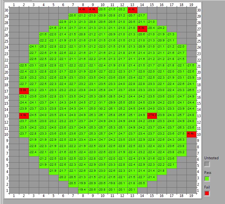
6 LMOSFET wafer & forward IV characteristics (6-inch X-fab)
:")


7 1200V 40mOhm MOSFET in TO-247 (6-inch X-fab): static characteristics 1 st engineering lot: performance to be further optimized Edge-termination and passivation are ok!
8 Inductive Load Switching Performance of the 1200V 40mOhm MOSFET in TO-247 (1 st Enginneering Lot) Normal Switching Characteristics Oscillations caused by the testing setup Turn-on: t r =44ns, Eon =538µJ Turn-off: t f =28ns, Eoff=201µJ Switching loss can be reduced by decreasing external gate resistor R G of the MOSFET.
9 1200V 40mOhm MOSFET in TO-247: preliminary reliability assessment Test stress condition duration sample size status HTGB VGS=+20V, VDS=0, Ta=150C 1000hrs 77 Pass HTGB VGS=-10V, VDS=0, Ta=150C 1000hrs 77 Pass HTRB VDS=960V, VGS=0, Ta=150C 1000hrs 77 Pass AC Tamb=121ºC, 100% RH, 205 Kpa, 96 Hrs 77 Pass
10 1200V 40mOhm MOSFET in TO-247: preliminary reliability assessment 1000 hr VDS=960V, VGS=0, Ta=150C UJM1204K HTRB 0hrs UJM1204K HTRB 1000hrs UJM1204K HTRB 0hrs UJM1204K HTRB 1000hrs T5 10mA (Vdc) T9 1.2kV,-5Vg (ua) SN# SN#
11 1200V 40mOhm MOSFET in TO-247: preliminary reliability assessment 1000 hr Vgs=+20/-10V, Vds=0V, Ta=150C HTGB (Vgs=+20V), 150 C HTGB (Vgs=-10V), 150 C UJM1204K HTGB +20VGS 0hrs UJM1204K HTGB +20VGS 1000hrs UJM1204K -10V HTGB 0hrs UJM1204K -10V HTGB 1000hrs T5 10mA (Vdc) T5 10mA (Vdc) SN# SN#
12 1200V 40mOhm MOSFET in TO-247: preliminary reliability assessment Ta=121C, Rh=100%, P=205kPa Pre AC Test Post AC Test Pre AC Test Post AC Test ua mA, V SN# SN#

13 1200V 40mOhm MOSFET in TO-247: preliminary UIS robustness evaluation Source metal Vgs=+12V Ohmic contact ILD Poly gate Ohmic contact Id=20A Vds~1700V P++ pbase N+ gate oxide N+ N CS-layer P++ pbase Vgs=-5V N- drift layer Vds=0V 150 μm N+ substrate drain metal Avalanche is clamped within each active cell L=5mH, E=1.4J Optimization of unit cell has been implemented in a new lot in order to suppress electric field in gate oxide and further improve UIS robustness
14 1200V 40mOhm MOSFET in TO-247: preliminary short-circuit capability assessment V DS = 600V I D 8us V GS = -5V to +15V 10us Device ID#: A23 External Rg = 22Ω Device ID#: A23 External Rg = 22Ω Two devices tested: Device #A23: Pass 8us SC testing, fail 10us SC testing Device #A26: Pass 8us and 10us SC testing
15 1200V 40mOhm MOSFET in TO-247: preliminary short-circuit capability assessment Device #A26: pass 10μs SC test Device #A23: fail at 10μs SC test Device unit cell layout will be optimized in a new lot; Vt increased in a new 1200V-40mOhm lot; SC-capability will be re-evaluated; 3300V SC-robust MOSFET lot is in the line;

16 Threshold Voltage Verification of the 2nd Engineering 1200V 40mOhm MOSFET Lot 1st Engr. Lot 2 nd Engr. Lot Wafer ID# The threshold voltage of the second qualification lot is basically in the target range. Threshold voltage, VTH (V)
17 10kV IGBT and MPS Development Status
18 USCi 10kV IGBT approach (4-inch fab) Emitter metal Emitter metal Ohmic contact ILD Poly gate Ohmic contac Ohmic contact ILD Poly gate Ohmic contac P++ pbase N+ gate oxide N+ N CS-layer P++ pbase P++ pbase N+ gate oxide N+ N CS-layer P++ pbase 150μm N-drift layer 150μm N-drift layer Standard N+ substrate N field-stop layer P+ injector collector metal After top-side MOS structure is formed, substrate is completely grinded away, N-type field-stop layer and P+ injector are ion-implanted, and laser-activated.
19 Laser-activated PN junction on Si-face Starting Epi: 11um of 8E15cm -3 N type (Si-face). Blanket nitrogen and aluminum co-implants Laser-assisted P & N dopant activation Diode mesa isolation and contact metal deposition (inset) Diode singulation, packaging and testing RT Qrr observed even at 50C; Increases with temperature Laser-activated PN diode have been formed!
20 First IGBT results (4-inch fab) Laser backside activated PN-junction knee voltage is present; C-face may be a challenge; P+ ohmiccontact may be poor; Narrow process window for laser activation;
21 High-voltage MPS diodes MPS diodes with 22mm 2 active area: bipolar operation is present, but diode performance on 150um (free-standing epi) has significant die-to-die and wafer-towafer variation 100um epi on standard N+ substrate, 8 kv 150um freestanding epi, 10 kv wafer vendor 1 wafer vendor 2 100um epi on standard N+ substrate, 8 kv wafer vendor 1 150um freestanding epi, 10 kv wafer vendor 2


22 10kV IGBT/MPS module design USCi in-house packaging low-cost and short lead time Voltage rating up to 10kV Small change to 15kV One solder joint chip to DBC Pressfit Power Leads Replaceable leads 60A max continuous 20A per pin Tjmax=175C ~ 200C Al wire bond 58 mm 66 mm 57 mm 22
23 Summary Established a 6-inch platform for large area 1200V MOSFETs targeting power modules New 1200V 40 mohm MOSFET lot is in the line (6-inch): Optimized unit cell structure and device layout expecting target performance; Process tuned; Increased Vt; Reduced Idsx leakage and improved shielding of gate oxide; Expect improved UIS and SC capability; 3300V SC-robust MOSFET lot is in the line (6-inch) Ion-implanted and laser-activated PN junction demonstrated on Si-face, although process is not reproducible and so far not successful on C-face IGBT process baseline demonstrated at 4-inch fab, including substrate removal, backside ion implantation and laser-anneal, although major technological challenges are unresolved Thick epi wafer warpage, LTV, TTV, and surface roughness are problematic on 4-inch; Laser-activation of p- and n-type dopants and ohmic contact formation on C-face of a free-standing low doped epi was not successful we may have to abandon original IGBT approach; New combined 6.5kV and 10kV IGBT/MOSFET lot is in the line (4-inch) Life-time enhancement; Optimized unit cell structure; Improved shielding of gate oxide; To be completed and tested;
Improving Totem-Pole PFC and On Board Charger performance with next generation components
 Improving Totem-Pole PFC and On Board Charger performance with next generation components Anup Bhalla 1) 1) United Silicon Carbide, Inc., 7 Deer Park Drive, Monmouth Jn., NJ USA E-mail: abhalla@unitedsic.com
SiC Cascodes and its advantages in power electronic applications
 SiC Cascodes and its advantages in power electronic applications WBG Power Conference, Munich, 5 th December 2017 Christopher Rocneanu Director Sales Europe and North America cro@unitedsic.com +4915121063411
Students: Yifan Jiang (Research Assistant) Siyang Liu (Visiting Scholar)
 Siyang Liu (Visiting Scholar)") Y9.FS1.1: SiC Power Devices for SST Applications Project Leader: Faculty: Dr. Jayant Baliga Dr. Alex Huang Students: Yifan Jiang (Research Assistant) Siyang Liu (Visiting Scholar) 1. Project Goals (a)
Y9.FS1.1: SiC Power Devices for SST Applications Project Leader: Faculty: Dr. Jayant Baliga Dr. Alex Huang Students: Yifan Jiang (Research Assistant) Siyang Liu (Visiting Scholar) 1. Project Goals (a)
Bias Stress Testing of SiC MOSFETs
 Bias Stress Testing of SiC MOSFETs Robert Shaw Manager, Test and Qualification August 15 th, 2014 Special thanks to the U.S. Department of Energy for funding this under SBIR DE-SC0011315. Outline Objectives
Progress Energy Distinguished University Professor Jay Baliga. April 11, Acknowledgements
 Progress Energy Distinguished University Professor Jay Baliga April 11, 2019 Acknowledgements 1 Outline SiC Power MOSFET Breakthroughs achieved at NCSU PRESiCE: SiC Power Device Manufacturing Technology
All-SiC Modules Equipped with SiC Trench Gate MOSFETs
 All-SiC Modules Equipped with SiC Trench Gate MOSFETs NAKAZAWA, Masayoshi * DAICHO, Norihiro * TSUJI, Takashi * A B S T R A C T There are increasing expectations placed on products that utilize SiC modules
4H-SiC V-Groove Trench MOSFETs with the Buried p + Regions
 ELECTRONICS 4H-SiC V-Groove Trench MOSFETs with the Buried p + Regions Yu SAITOH*, Toru HIYOSHI, Keiji WADA, Takeyoshi MASUDA, Takashi TSUNO and Yasuki MIKAMURA ----------------------------------------------------------------------------------------------------------------------------------------------------------------------------------------------------------------------------------------------------------
PWRLITE LD1010D High Performance N-Ch Vertical Power JFET Transistor with Schottky G D S
 www.lovoltech.com PWRLITE LD11D High Performance N-Ch Vertical Power JFET Transistor with Schottky Features Trench Power JFET with low threshold voltage Vth. Device fully ON with Vgs =.7V Optimum for Low
SGP100N09T. Symbol Parameter SGP100N09T Unit. 70* -Continuous (TA = 100 )
") SUPER-SEMI SUPER-MOSFET Super Gate Metal Oxide Semiconductor Field Effect Transistor 100V Super Gate Power Transistor SG*100N09T Rev. 1.01 Jun. 2016 SGP100N09T 100V N-Channel MOSFET Description The SG-MOSFET
SUPER-SEMI SUPER-MOSFET Super Gate Metal Oxide Semiconductor Field Effect Transistor 100V Super Gate Power Transistor SG*100N09T Rev. 1.01 Jun. 2016 SGP100N09T 100V N-Channel MOSFET Description The SG-MOSFET
ECSE-6300 IC Fabrication Laboratory Lecture 7 MOSFETs. Lecture Outline
 ECSE-6300 IC Fabrication Laboratory Lecture 7 MOSFETs Prof. Rensselaer Polytechnic Institute Troy, NY 12180 Office: CII-6229 Tel.: (518) 276-2909 e-mails: luj@rpi.edu http://www.ecse.rpi.edu/courses/s16/ecse
ECSE-6300 IC Fabrication Laboratory Lecture 9 MOSFETs. Lecture Outline
 ECSE-6300 IC Fabrication Laboratory Lecture 9 MOSFETs Prof. Rensselaer Polytechnic Institute Troy, NY 12180 Office: CII-6229 Tel.: (518) 276-2909 e-mails: luj@rpi.edu http://www.ecse.rpi.edu/courses/s18/ecse
Evolution of SiC MOSFETs at Cree Performance and Reliability
 Evolution of SiC MOSFETs at Cree Performance and Reliability Brett Hull :: August 13, 2015 Dan Lichtenwalner, Vipin Pala, Edward VanBrunt, Sei- Hyung Ryu, Jim Richmond, Leo Wang, Philip Butler, Don Gajewski,
Power MOSFET Zheng Yang (ERF 3017,
 ECE442 Power Semiconductor Devices and Integrated Circuits Power MOSFET Zheng Yang (ERF 3017, email: yangzhen@uic.edu) Evolution of low-voltage (
PWRLITE LU1014D High Performance N-Channel POWERJFET TM with PN Diode
 PWRLITE LU114D High Performance N-Channel POWERJFET TM with PN Diode Features Superior gate charge x Rdson product (FOM) Trench Power JFET with low threshold voltage Vth. Device fully ON with Vgs =.7V
Failure Mechanisms and Robustness of Wide Band-Gap Devices under short-circuits and unclamped inductive switching
 Failure Mechanisms and Robustness of Wide Band-Gap Devices under short-circuits and unclamped inductive switching Stéphane Lefebvre (Cnam), Zoubir Khatir (IFSTTAR), Mounira Berkani (UPEC), Denis Labrousse
Three Terminal Devices
 Three Terminal Devices - field effect transistor (FET) - bipolar junction transistor (BJT) - foundation on which modern electronics is built - active devices - devices described completely by considering
Y9.FS1.2.1: GaN Low Voltage Power Device Development. Sizhen Wang (Ph.D., EE)
") Y9.FS1.2.1: GaN Low Voltage Power Device Development Faculty: Students: Alex. Q. Huang Sizhen Wang (Ph.D., EE) 1. Project Goals The overall objective of the GaN power device project is to fabricate and
Y9.FS1.2.1: GaN Low Voltage Power Device Development Faculty: Students: Alex. Q. Huang Sizhen Wang (Ph.D., EE) 1. Project Goals The overall objective of the GaN power device project is to fabricate and
Monolith Semiconductor Inc. ARL SiC MOSFET Workshop 14 August 2015
 Monolith Semiconductor Inc. ARL SiC MOSFET Workshop 14 August 2015 Kevin Matocha, President 408 Fannin Ave Round Rock, TX 78664 Bringing SiC to our World. Acknowledgments Office of Science SBIR Prog. Office
Unit III FET and its Applications. 2 Marks Questions and Answers
 Unit III FET and its Applications 2 Marks Questions and Answers 1. Why do you call FET as field effect transistor? The name field effect is derived from the fact that the current is controlled by an electric
Integrated diodes. The forward voltage drop only slightly depends on the forward current. ELEKTRONIKOS ĮTAISAI
 1 Integrated diodes pn junctions of transistor structures can be used as integrated diodes. The choice of the junction is limited by the considerations of switching speed and breakdown voltage. The forward
Wide Band-Gap Power Device
 Wide Band-Gap Power Device 1 Contents Revisit silicon power MOSFETs Silicon limitation Silicon solution Wide Band-Gap material Characteristic of SiC Power Device Characteristic of GaN Power Device 2 1
COLLECTOR DRAIN BASE GATE EMITTER. Applying a voltage to the Gate connection allows current to flow between the Drain and Source connections.
 MOSFETS Although the base current in a transistor is usually small (< 0.1 ma), some input devices (e.g. a crystal microphone) may be limited in their output. In order to overcome this, a Field Effect Transistor
PFP15T140 / PFB15T140
 FEATURES 1% EAS Test Super high density cell design Extremely Low Intrinsic Capacitances Remarkable Switching Characteristics Extended Safe Operating Area Lower R DS(ON) : 6. mω (Typ.) @ =1V 15V N-Channel
Robustness Study of SiC MOSFET Under Harsh Electrical and Thermal Constraints
 Robustness Study of SiC MOSFET Under Harsh Electrical and Thermal Constraints To an in-depth physical failure analysis Safa Mbarek, Pascal Dherbécourt, Olivier Latry, François Fouquet* University of Rouen,
Cascode Configuration Eases Challenges of Applying SiC JFETs
 Application Note USCi_AN0004 March 2016 Cascode Configuration Eases Challenges of Applying SiC JFETs John Bendel Abstract The high switching speeds and low R DS(ON) of high-voltage SiC JFETs can significantly
EE 5611 Introduction to Microelectronic Technologies Fall Thursday, September 04, 2014 Lecture 02
 EE 5611 Introduction to Microelectronic Technologies Fall 2014 Thursday, September 04, 2014 Lecture 02 1 Lecture Outline Review on semiconductor materials Review on microelectronic devices Example of microelectronic
Study on Fabrication and Fast Switching of High Voltage SiC JFET
 Advanced Materials Research Online: 2013-10-31 ISSN: 1662-8985, Vol. 827, pp 282-286 doi:10.4028/www.scientific.net/amr.827.282 2014 Trans Tech Publications, Switzerland Study on Fabrication and Fast Switching
Lecture 020 ECE4430 Review II (1/5/04) Page 020-1
 Page 020-1") Lecture 020 ECE4430 Review II (1/5/04) Page 020-1 LECTURE 020 ECE 4430 REVIEW II (READING: GHLM - Chap. 2) Objective The objective of this presentation is: 1.) Identify the prerequisite material as taught
Lecture 020 ECE4430 Review II (1/5/04) Page 020-1 LECTURE 020 ECE 4430 REVIEW II (READING: GHLM - Chap. 2) Objective The objective of this presentation is: 1.) Identify the prerequisite material as taught
SI-TECH SEMICONDUCTOR CO.,LTD S85N10R/S
 N-Channel MOSFET Features 85V,100A,Rds(on)(typ)=5.8mΩ @Vgs=10V High Ruggedness Fast Switching 100% Avalanche Tested Improved dv/dt Capability General Description This Power MOSFET is produced using Si-Tech
PKP3105. P-Ch 30V Fast Switching MOSFETs
 Super Low Gate Charge % EAS Guaranteed Green Device Available Excellent CdV/dt effect decline Advanced high cell density Trench technology Product Summary BVDSS RDSON ID -3V mω -6A Description TO22 Pin
MEI. 20V P-Channel Enhancement-Mode MOSFET P2301BLT1G. Features. Simple Drive Requirement Small Package Outline Surface Mount Device G 1 2 V DS -20
 V P-Channel Enhancement-Mode MOSFET VDS= -V RDS(ON), Vgs@-.5V, Ids@-.A = mω RDS(ON), Vgs@-.5V, Ids@-.A = 15 mω Features Advanced trench process technology High Density Cell Design For Ultra Low On-Resistance
Fundamentals of Power Semiconductor Devices
 В. Jayant Baliga Fundamentals of Power Semiconductor Devices 4y Spri ringer Contents Preface vii Chapter 1 Introduction 1 1.1 Ideal and Typical Power Switching Waveforms 3 1.2 Ideal and Typical Power Device
1200 V SiC Super Junction Transistors operating at 250 C with extremely low energy losses for power conversion applications
 1200 V SiC Super Junction Transistors operating at 250 C with extremely low energy losses for power conversion applications Ranbir Singh, Siddarth Sundaresan, Eric Lieser and Michael Digangi GeneSiC Semiconductor,
AONS V N-Channel MOSFET
 AONS3634 3V N-Channel MOSFET General Description Trench Power MOSFET technology Low R DS(ON) Low Gate Charge High Current Capability RoHS and Halogen-Free Compliant Product Summary V DS I D (at V GS =V)
(a) All-SiC 2-in-1 module
 All-SiC 2-in-1 module") All-SiC -in- Module CHONABAYASHI, Mikiya * OTOMO, Yoshinori * KARASAWA, Tatsuya * A B S T R A C T Fuji Electric has developed an utilizing a SiC device that has been adopted in the development of a high-performance
All-SiC -in- Module CHONABAYASHI, Mikiya * OTOMO, Yoshinori * KARASAWA, Tatsuya * A B S T R A C T Fuji Electric has developed an utilizing a SiC device that has been adopted in the development of a high-performance
UNIT 3: FIELD EFFECT TRANSISTORS
 FIELD EFFECT TRANSISTOR: UNIT 3: FIELD EFFECT TRANSISTORS The field effect transistor is a semiconductor device, which depends for its operation on the control of current by an electric field. There are
VDSS (V) 650 V(TR)DSS (V) 800. RDS(on)eff (mω) max* 85. QRR (nc) typ 90. QG (nc) typ 10
 650 V(TR)DSS (V) 800. RDS(on)eff (mω) max* 85. QRR (nc) typ 90. QG (nc) typ 10") TP65H070L Series 650V GaN FET PQFN Series Preliminary Description The TP65H070L 650V, 72mΩ Gallium Nitride (GaN) FET are normally-off devices. It combines state-of-the-art high voltage GaN HEMT and low
TP65H070L Series 650V GaN FET PQFN Series Preliminary Description The TP65H070L 650V, 72mΩ Gallium Nitride (GaN) FET are normally-off devices. It combines state-of-the-art high voltage GaN HEMT and low
Symbol Parameter Rating Units VDS Drain-Source Voltage 30 V VGS Gate-Source Voltage ±20 V
 % EAS Guaranteed Green Device Available Super Low Gate Charge Excellent CdV/dt effect decline Advanced high cell density Trench technology Product Summary BVDSS RDSON ID 3V mω A Description TO Pin Configuration
High Voltage Normally-off GaN MOSC- HEMTs on Silicon Substrates for Power Switching Applications
 High Voltage Normally-off GaN MOSC- HEMTs on Silicon Substrates for Power Switching Applications Zhongda Li, John Waldron, Shinya Takashima, Rohan Dayal, Leila Parsa, Mona Hella, and T. Paul Chow Department
Efficiency improvement with silicon carbide based power modules
 Efficiency improvement with silicon carbide based power modules Zhang Xi*, Daniel Domes*, Roland Rupp** * Infineon Technologies AG, Max-Planck-Straße 5, 59581 Warstein, Germany ** Infineon Technologies
Design cycle for MEMS
 Design cycle for MEMS Design cycle for ICs IC Process Selection nmos CMOS BiCMOS ECL for logic for I/O and driver circuit for critical high speed parts of the system The Real Estate of a Wafer MOS Transistor
A new Vertical JFET Technology for Harsh Radiation Applications
 A New Vertical JFET Technology for Harsh Radiation Applications ISPS 2016 1 A new Vertical JFET Technology for Harsh Radiation Applications A Rad-Hard switch for the ATLAS Inner Tracker P. Fernández-Martínez,
Student Lecture by: Giangiacomo Groppi Joel Cassell Pierre Berthelot September 28 th 2004
 Student Lecture by: Giangiacomo Groppi Joel Cassell Pierre Berthelot September 28 th 2004 Lecture outline Historical introduction Semiconductor devices overview Bipolar Junction Transistor (BJT) Field
SiC MOSFET Reliability
 SiC MOSFET Reliability - Oxide lifetime / breakdown - High-energy Neutron radiation ruggedness Daniel J Lichtenwalner, Edward Van Brunt, Shadi Sabri, Jim Richmond, Brett Hull, David Grider, Scott Allen,
Features. Symbol Parameter Typ. Max. Unit RθJA Thermal Resistance Junction to ambient /W RθJC Thermal Resistance Junction to Case
 General Description These N-Channel enhancement mode power field effect transistors are planar stripe, DMOS technology. This advanced technology has been especially tailored to minimize on-state resistance,
INTRODUCTION: Basic operating principle of a MOSFET:
 INTRODUCTION: Along with the Junction Field Effect Transistor (JFET), there is another type of Field Effect Transistor available whose Gate input is electrically insulated from the main current carrying
Power Matters Microsemi SiC Products
 Microsemi SiC Products James Kerr Director of Marketing Power Discrete Products Microsemi Power Products MOSFETs (100V-1200V) Highest Performance SiC MOSFETs 1200V MOSFETs FREDFETs (MOSFET with fast body
8 S1, D2. Storage Temperature Range Soldering Temperature, for 10 seconds 300 (1.6mm from case )
") Co-Pack Dual N-channel HEXFET Power MOSFET and Schottky Diode Ideal for Synchronous Buck DC-DC Converters Up to A Peak Output Low Conduction Losses Low Switching Losses Low Vf Schottky Rectifier D D 2
Co-Pack Dual N-channel HEXFET Power MOSFET and Schottky Diode Ideal for Synchronous Buck DC-DC Converters Up to A Peak Output Low Conduction Losses Low Switching Losses Low Vf Schottky Rectifier D D 2
Parameter Symbol Limit Unit IDM 20 A T A = PD T A =100
 Features: Super high dense cell design for low R DS(ON) Rugged and reliable Surface Mount Package B VDSS =20V, R DS(ON) =24.5mΩ ID=6A Application DC-DC converters Power management in portable and Battery-powered
Is Now Part of. To learn more about ON Semiconductor, please visit our website at
 Is Now Part of To learn more about ON Semiconductor, please visit our website at www.onsemi.com Please note: As part of the Fairchild Semiconductor integration, some of the Fairchild orderable part numbers
PDN001N60S. 600V N-Channel MOSFETs BVDSS RDSON ID 600V A S G. General Description. Features. SOT23-3S Pin Configuration.
 General Description These N-Channel enhancement mode power field effect transistors are planar stripe, DMOS technology. This advanced technology has been especially tailored to minimize on-state resistance,
Advanced Power MOSFET Concepts
 В. Jayant Baliga Advanced Power MOSFET Concepts Springer Contents 1 Introduction 1 1.1 Ideal Power Switching Waveforms 2 1.2 Ideal and Typical Power MOSFET Characteristics 3 1.3 Typical Power MOSFET Structures
S2 6 1 S1 3 D2 2 G1. Pin configuration (Top view) Parameter Symbol 10 S Steady State Unit Drain-Source Voltage V DS +20 Gate-Source Voltage V GS 6
 Parameter Symbol 10 S Steady State Unit Drain-Source Voltage V DS +20 Gate-Source Voltage V GS 6") Descriptions Features and Applications The SOT-363 is N-Channel enhancement MOS Field Effect Transistor. Uses advanced trench technology and design to provide excellent R DS (ON) with low gate charge.
Descriptions Features and Applications The SOT-363 is N-Channel enhancement MOS Field Effect Transistor. Uses advanced trench technology and design to provide excellent R DS (ON) with low gate charge.
RU1HE16L. N-Channel Advanced Power MOSFET MOSFET. Applications. Absolute Maximum Ratings TO252. Power Management. N-Channel MOSFET
 N-Channel Advanced Power MOSFET MOSFET Features 100V/16A, RDS (ON) =70mΩ(Typ.)@VGS=10V RDS (ON) =85mΩ(Typ.)@VGS=4.5V Pin Description Super High Dense Cell Design ESD protected Reliable and Rugged Lead
Design considerations for chargecompensated. medium-voltage range. Ralf Siemieniec, Cesar Braz, Oliver Blank Infineon Technologies Austria AG
 Design considerations for chargecompensated power MOSFET in the medium-voltage range Ralf Siemieniec, Cesar Braz, Oliver Blank Infineon Technologies Austria AG Outline 1 Introduction 2 Application requirements
Impact of Basal Plane Dislocations and Ruggedness of 10 kv 4H-SiC Transistors
 11th International MOS-AK Workshop (co-located with the IEDM and CMC Meetings) Silicon Valley, December 5, 2018 Impact of Basal Plane Dislocations and Ruggedness of 10 kv 4H-SiC Transistors *, A. Kumar,
Rugged 1.2 KV SiC MOSFETs Fabricated in High-Volume 150mm CMOS Fab
 Rugged 1.2 KV SiC MOSFETs Fabricated in High-Volume 150mm CMOS Fab Agenda Motivation for SiC Devices SiC MOSFET Market Status High-Volume 150mm Process Performance / Ruggedness Validation Static characteristics
FKD4903. N-Ch and P-Ch Fast Switching MOSFETs
 FKD93 % EAS Guaranteed Green Device Available Super Low Gate Charge Excellent CdV/dt effect decline Advanced high cell density Trench technology Product Summary BVDSS RDSON ID V 3mΩ 3A -V 5mΩ -A Description
Field-Effect Transistor (FET) is one of the two major transistors; FET derives its name from its working mechanism;
 is one of the two major transistors; FET derives its name from its working mechanism;") Chapter 3 Field-Effect Transistors (FETs) 3.1 Introduction Field-Effect Transistor (FET) is one of the two major transistors; FET derives its name from its working mechanism; The concept has been known
Chapter 3 Field-Effect Transistors (FETs) 3.1 Introduction Field-Effect Transistor (FET) is one of the two major transistors; FET derives its name from its working mechanism; The concept has been known
Microsemi SiC MOSFETs
 Microsemi SiC MOSFETs Francis K Chai April 15 th -16 th, 2015 Outline 1700V wafer- level data Starting epitaxial wafers Technology development Benchmark of SiC MOSFET by Microsemi against competitors DC
SM1A16PSU/UB. Features. Ordering and Marking Information. P-Channel Enhancement Mode MOSFET -100V/-13A, R DS(ON) =-10V
 =-10V") P-Channel Enhancement Mode MOSFET Features Pin Configuration -0V/-13A, R DS(ON) =205mΩ (max.) @ V GS =-V R DS(ON) =300mΩ (max.) @ V GS =-4V Reliable and Rugged D S G S D G Lead Free and Green Devices Available
P-Channel Enhancement Mode MOSFET Features Pin Configuration -0V/-13A, R DS(ON) =205mΩ (max.) @ V GS =-V R DS(ON) =300mΩ (max.) @ V GS =-4V Reliable and Rugged D S G S D G Lead Free and Green Devices Available
GaN based Power Devices. Michael A. Briere. RPI CFES Conference
 GaN based Power Devices Michael A. Briere ACOO Enterprises LLC Under contract to International Rectifier RPI CFES Conference January 25, 2013 1 Motivation : Potential Energy Savings Worldwide M.A. Briere
Among the lowest R DS(on) on the market Excellent FoM (figure of merit) Low C rss /C iss ratio for EMI immunity High avalanche ruggedness
 on the market Excellent FoM (figure of merit) Low C rss /C iss ratio for EMI immunity High avalanche ruggedness") N-channel 100 V, 5 mω typ., 107 A, STripFET F7 Power MOSFET in a PowerFLAT 5x6 package Features Order code V DS R DS(on) max. I D P TOT STL110N10F7 100 V 6 mω 107 A 136 W Among the lowest R DS(on) on the
N-channel 100 V, 5 mω typ., 107 A, STripFET F7 Power MOSFET in a PowerFLAT 5x6 package Features Order code V DS R DS(on) max. I D P TOT STL110N10F7 100 V 6 mω 107 A 136 W Among the lowest R DS(on) on the
Talk1: Overview of Power Devices and Technology Trends. Talk 2: Devices and Technologies for HVIC
 Talk1: Overview of Power Devices and Technology Trends Talk 2: Devices and Technologies for HVIC Prof. Florin Udrea Cambridge University Taiwan, January 2010 1 Outline Talk 1: Overview of Power Devices
Field Effect Transistors
 Chapter 5: Field Effect Transistors Slide 1 FET FET s (Field Effect Transistors) are much like BJT s (Bipolar Junction Transistors). Similarities: Amplifiers Switching devices Impedance matching circuits
I E I C since I B is very small
 Figure 2: Symbols and nomenclature of a (a) npn and (b) pnp transistor. The BJT consists of three regions, emitter, base, and collector. The emitter and collector are usually of one type of doping, while
Data Sheet Explanation
 Data Sheet Explanation V1.2 2014-04 Edition 2014-01 Published by Infineon Technologies AG, 81726 Munich, Germany. 2014 Infineon Technologies AG All Rights Reserved. LEGAL DISCLAIMER THE INFORMATION GIVEN
Q1. Explain the construction and principle of operation of N-Channel and P-Channel Junction Field Effect Transistor (JFET).
.") Q. Explain the construction and principle of operation of N-Channel and P-Channel Junction Field Effect Transistor (JFET). Answer: N-Channel Junction Field Effect Transistor (JFET) Construction: Drain(D)
Q. Explain the construction and principle of operation of N-Channel and P-Channel Junction Field Effect Transistor (JFET). Answer: N-Channel Junction Field Effect Transistor (JFET) Construction: Drain(D)
Review of Power IC Technologies
 Review of Power IC Technologies Ettore Napoli Dept. Electronic and Telecommunication Engineering University of Napoli, Italy Introduction The integration of Power and control circuitry is desirable for
Lecture Notes. Emerging Devices. William P. Robbins Professor, Dept. of Electrical and Computer Engineering University of Minnesota.
 Lecture Notes Emerging Devices William P. Robbins Professor, Dept. of Electrical and Computer Engineering University of Minnesota Outline Power JFET Devices Field-Controlled Thyristor MOS-Controlled Thyristor
EPC2107 Enhancement-Mode GaN Power Transistor Half-Bridge with Integrated Synchronous Bootstrap
 EPC7 Enhancement-Mode GaN Power Transistor Half-Bridge with Integrated Synchronous Bootstrap V DSS, V R DS(on), 9 m I D,.7 A EFFICIENT POWER CONVERSION HAL EPC7 Gallium Nitride is grown on Silicon Wafers
T C =25 unless otherwise specified. Symbol Parameter Value Units V DSS Drain-Source Voltage 40 V
 40V N-Channel Trench MOSFET June 205 BS = 40 V R DS(on) typ = 3.3mΩ = 30 A FEATURES Originative New Design Superior Avalanche Rugged Technology Excellent Switching Characteristics Unrivalled Gate Charge
Features. Description. AM01475v1_Tab. Table 1: Device summary Order code Marking Package Packing STW240N10F7 240N10F7 TO-247 Tube
 N-channel 100 V, 2.6 mω typ., 180 A, STripFET F7 Power MOSFET in a TO-247 package Datasheet - production data Features Order code VDS RDS(on) max. ID 100 V 3.0 mω 180 A 1 2 3 Among the lowest RDS(on) on
TO-252 Pin Configuration
 WSF46 General Description The WSF46 is the highest performance trench with extreme high cell density, which provide excellent RDSON and gate charge for most of the synchronous buck converter applications.
Features Package Applications Key Specifications Internal Equivalent Circuit Absolute maximum ratings
 DKG2 Aug. 2 Features Low on-state resistance Built-in gate protection diode SMD PKG Package TO252 Applications DC / DC converter Switching Internal Equivalent Circuit D(2) Key Specifications V (BR)DSS
VDSS (V) 650. V(TR)DSS (V) 800 RDS(on)eff (mω) max* 180. QRR (nc) typ 52. QG (nc) typ 6.2
 650. V(TR)DSS (V) 800 RDS(on)eff (mω) max* 180. QRR (nc) typ 52. QG (nc) typ 6.2") 650V GaN FET PQFN Series Not recommended for new designs Description The TPH3206L Series 650V, 150mΩ Gallium Nitride (GaN) FETs are normally-off devices. They combine state-of-the-art high voltage GaN
650V GaN FET PQFN Series Not recommended for new designs Description The TPH3206L Series 650V, 150mΩ Gallium Nitride (GaN) FETs are normally-off devices. They combine state-of-the-art high voltage GaN
SMC6216SN. Single N-Channel MOSFET FEATURES VDS = 60V, ID = 3.5A DESCRIPTION APPLICATIONS PART NUMBER INFORMATION
 SMC66SN Single N-Channel MOSFET DESCRIPTION SMC66 is the N-Channel enhancement mode power field effect transistors are using trench DMOS technology. This advanced trench technology devices are well suited
Package Code P : TO-220FB-3L. Date Code YYXXX WW
 N-Channel Enhancement Mode MOSFET Features Pin Description 3V/ 29A R DS(ON) =.6mΩ (typ.) @ =V % EAS Guaranteed Super Low Gate Charge Excellent CdV/dt effect decline Advanced high cell density Trench technology
Features. Description. Table 1: Device summary Order code Marking Package Packaging STR1P2UH7 1L2U SOT-23 Tape and reel
 P-channel 20 V, 0.087 Ω typ., 1.4 A STripFET H7 Power MOSFET in a SOT-23 package Datasheet - production data Features Order code VDS RDS(on) max ID STR1P2UH7 20 V 0.1 Ω @ 4.5 1.4 A Very low on-resistance
Implantation-Free 4H-SiC Bipolar Junction Transistors with Double Base Epi-layers
 Implantation-Free 4H-SiC Bipolar Junction Transistors with Double Base Epi-layers Jianhui Zhang, member, IEEE, Xueqing, Li, Petre Alexandrov, member, IEEE, Terry Burke, member, IEEE, and Jian H. Zhao,
AE53/AC53/AT53/AE103 ELECT. DEVICES & CIRCUITS DEC 2015
 Q.2 a. By using Norton s theorem, find the current in the load resistor R L for the circuit shown in Fig.1. (8) Fig.1 IETE 1 b. Explain Z parameters and also draw an equivalent circuit of the Z parameter
IGBT Technologies and Applications Overview: How and When to Use an IGBT Vittorio Crisafulli, Apps Eng Manager. Public Information
 IGBT Technologies and Applications Overview: How and When to Use an IGBT Vittorio Crisafulli, Apps Eng Manager Agenda Introduction Semiconductor Technology Overview Applications Overview: Welding Induction
Comparison of Different Cell Concepts for 1200V- NPT-IGBT's
 Comparison of Different Cell Concepts for 12V- NPT-IGBT's R.Siemieniec, M.Netzel, R. Herzer, D.Schipanski Abstract - IGBT's are relatively new power devices combining bipolar and unipolar properties. In
Package Code. Handling Code. Assembly Material
 P-Channel Enhancement Mode MOSFET Features Pin Description -2V/-4.9A, R DS(ON) =43mΩ (Max.) @ V GS =-4.5V R DS(ON) =58mΩ (Max.) @ V GS =-2.5V R DS(ON) =88mΩ (Max.) @ V GS =-1.8V 1% UIS + R g Tested Reliable
T-series and U-series IGBT Modules (600 V)
") T-series and U-series IGBT Modules (6 V) Seiji Momota Syuuji Miyashita Hiroki Wakimoto 1. Introduction The IGBT (insulated gate bipolar transistor) module is the most popular power device in power electronics
T-series and U-series IGBT Modules (6 V) Seiji Momota Syuuji Miyashita Hiroki Wakimoto 1. Introduction The IGBT (insulated gate bipolar transistor) module is the most popular power device in power electronics
GaN Based Power Conversion: Moving On! Tim McDonald APEC Key Component Technologies for Power Electronics in Electric Drive Vehicles
 1 GaN Based Power Conversion: Moving On! Key Component Technologies for Power Electronics in Electric Drive Vehicles Tim McDonald APEC 2013 2 Acknowledgements Collaborators: Tim McDonald (1), Han S. Lee
VDS (V) min 650 VTDS (V) max 800 RDS(on) (mω) max* 60. Qrr (nc) typ 136. Qg (nc) typ 28. * Dynamic RDS(on)
 min 650 VTDS (V) max 800 RDS(on) (mω) max* 60. Qrr (nc) typ 136. Qg (nc) typ 28. * Dynamic RDS(on)") 650V Cascode GaN FET in TO-247 (source tab) Description The TPH3205WSB 650V, 49mΩ gallium nitride (GaN) FET is a normally-off device. Transphorm GaN FETs offer better efficiency through lower gate charge,
650V Cascode GaN FET in TO-247 (source tab) Description The TPH3205WSB 650V, 49mΩ gallium nitride (GaN) FET is a normally-off device. Transphorm GaN FETs offer better efficiency through lower gate charge,
IPS0551T FULLY PROTECTED POWER MOSFET SWITCH. L oad. Product Summary
 Data Sheet No. PD616-C FULLY PROTECTED POWER MOSFET SWITCH Features Over temperature shutdown Over current shutdown Active clamp Low current & logic level input E.S.D protection Description The is a fully
IRFI4212H-117P. Description. Key Parameters g V DS 100 V R DS(ON) 10V 58 m: Q g typ. 12 nc Q sw typ. 6.9 nc R G(int) typ. 3.
 10V 58 m: Q g typ. 12 nc Q sw typ. 6.9 nc R G(int) typ. 3.") DIGITAL AUDIO MOSFET PD - 97249A IRFI422H-7P Features Ÿ Integrated half-bridge package Ÿ Reduces the part count by half Ÿ Facilitates better PCB layout Ÿ Key parameters optimized for Class-D audio amplifier
DIGITAL AUDIO MOSFET PD - 97249A IRFI422H-7P Features Ÿ Integrated half-bridge package Ÿ Reduces the part count by half Ÿ Facilitates better PCB layout Ÿ Key parameters optimized for Class-D audio amplifier
WBG Device Reliability Team Short-Circuit Robustness Testing of SiC Power MOSFETs
 2016 August WBG Device Reliability Team Short-Circuit Robustness Testing of SiC Power MOSFETs Ron Green, Ph. D. Damian Urciuoli Aivars Lelis, Ph. D. Daniel Habersat Franklin Nouketcha Outline Introduction
RU75N08S. N-Channel Advanced Power MOSFET. Applications. Absolute Maximum Ratings TO-263. Switching Application Systems.
 N-Channel Advanced Power MOSFET Features 75V/80A, RDS (ON) =8mΩ (typ.) @VGS=10V Pin Description Ultra Low On-Resistance Exceptional dv/dt capability Fast Switching and Fully Avalanche Rated 100% avalanche
How to Design an R g Resistor for a Vishay Trench PT IGBT
 VISHAY SEMICONDUCTORS www.vishay.com Rectifiers By Carmelo Sanfilippo and Filippo Crudelini INTRODUCTION In low-switching-frequency applications like DC/AC stages for TIG welding equipment, the slow leg
SMD Type. P-Channel Enhancement MOSFET IRLML6401 (KRLML6401) Features. Absolute Maximum Ratings Ta = 25
 Features. Absolute Maximum Ratings Ta = 25") SMD Type P-Channel Enhancement IRLML640 (KRLML640) Features Ultra low on-resistance. P-Channel. Fast switching. 2.4 - + SOT-23 3 2.9 - + 0.4 - + 2.3 - + 0.55 0.4 Unit: mm 0.95 - +.9 - + -0.0 +0.05 0-0.38
SMD Type P-Channel Enhancement IRLML640 (KRLML640) Features Ultra low on-resistance. P-Channel. Fast switching. 2.4 - + SOT-23 3 2.9 - + 0.4 - + 2.3 - + 0.55 0.4 Unit: mm 0.95 - +.9 - + -0.0 +0.05 0-0.38
GaN MMIC PAs for MMW Applicaitons
 GaN MMIC PAs for MMW Applicaitons Miroslav Micovic HRL Laboratories LLC, 311 Malibu Canyon Road, Malibu, CA 9265, U. S. A. mmicovic@hrl.com Motivation for High Frequency Power sources 6 GHz 11 GHz Frequency
PERSPECTIVES FOR DISRUPTIVE 200MM/8-INCH GAN POWER DEVICE AND GAN-IC TECHNOLOGY DR. DENIS MARCON SR. BUSINESS DEVELOPMENT MANAGER
 PERSPECTIVES FOR DISRUPTIVE 200MM/8-INCH GAN POWER DEVICE AND GAN-IC TECHNOLOGY DR. DENIS MARCON SR. BUSINESS DEVELOPMENT MANAGER What I will show you today 200mm/8-inch GaN-on-Si e-mode/normally-off technology
TPH3205WSB. 650V Cascode GaN FET in TO-247 (source tab)
") 650V Cascode GaN FET in TO-247 (source tab) Description The TPH3205WSB 650V, 52mΩ gallium nitride (GaN) FET is a normally-off device. Transphorm GaN FETs offer better efficiency through lower gate charge,
650V Cascode GaN FET in TO-247 (source tab) Description The TPH3205WSB 650V, 52mΩ gallium nitride (GaN) FET is a normally-off device. Transphorm GaN FETs offer better efficiency through lower gate charge,
Switch mode power supplies Low gate charge. Power factor correction modules Low intrinsic capacitance
 Description United Silicon Carbide's cascode products co-package its highperformance F3 SiC fast JFETs with a cascode optimized MOSFET to produce the only standard gate drive SiC device in the market today.
Chapter 3 Basics Semiconductor Devices and Processing
 Chapter 3 Basics Semiconductor Devices and Processing 1 Objectives Identify at least two semiconductor materials from the periodic table of elements List n-type and p-type dopants Describe a diode and
Design of a Rugged 60V VDMOS Transistor
 Design of a Rugged 60V VDMOS Transistor H. P. Edward Xu, Olivier P. Trescases, I-Shan Michael Sun, Dora Lee, Wai Tung Ng*, Kenji Fukumoto, Akira Ishikawa, Yuichi Furukawa, Hisaya Imai, Takashi Naito, Nobuyuki