CHAPTER 6 Radio Circuits and Systems
|
|
|
- Agnes Dixon
- 6 years ago
- Views:
Transcription
1 6.1 AMPLIFIERS (page 6-1) CHAPTER 6 Radio Circuits and Systems AMPLIFIER GAIN (page 6-2) INPUT AND OUTPUT IMPEDANCE (page 6-2) DISCRETE DEVICE AMPLIFIERS (page 6-2) BASIC CIRCUITS (page 6-2) COMMON-EMITTER CIRCUIT (PAGE 6-3) Equivalent to Figure E7-1 R 4 47K 4.7K + 5µF R 3 + C 3 4.7K 470Ω 25 µf V E You can recognize the common-emitter amplifier circuit by the value for the resistance in the emitter circuit (R 3 or R E ) being much smaller (or even absent) than that in the collector circuit (R 4 or R L ) or the emitter resistor being bypassed with a capacitor (C 3 ). Question E7B12: What type of amplifier circuit is shown in Figure E7-1? Answer: Common emitter On a common-emitter amplifier the output signal is 180 out of phase with the input signal. Resisters R 1 and R 2 form a voltage divider to provide a stable operating point. (This operating point is usually chosen so that the Emitter voltage (V E ) is one volt which means the Base voltage (V B ) is at 1.7 volts on a silicon transistor.) Wednesday, October 19,
2 (The example in the manual has the bias voltage at 0.82 volts which means the emitter is at 0.12 volts.) (A better solution would be to replace R 1 with a 27K ohm resistor.) This is called Fixed Bias. Question E7B10: In Figure E7-1, what is the purpose of R1 and R2? Answer: Fixed bias Common-emitter circuits are subject to thermal runaway. As forward bias is increased, the collector current and gain are higher, and that makes the temperature of the transistors junctions higher. As temperature increases so does the gain of the transistor, causing collector-emitter current to increase even more. Eventually transistor junctions are overheated and destroyed. Some kind of negative feedback or bias stabilization is required to prevent this from happening. One solution is to add resistance in the emitter circuit (R 3 ) to create degenerative emitter feed back or self-bias. Question E7B11: In Figure E7-1, what is the purpose of R3? Answer: Self bias As emitter current increases, so does the DC voltage across R 3. This increasing voltage reduces the base-emitter forward bias established by R 1 and R 2 reducing emitter current. The resulting balancing act stabilizing the transistor s operating point and prevents thermal runaway. Again, Use a resistor in series with the emitter to prevent thermal runaway in a bipolar transistor amplifier. Question E7B15: What is one way to prevent thermal runaway in a bipolar transistor amplifier? Answer: Use a resistor in series with the emitter [(first paragraph on page 6-4) The first resistance is the parallel combination of an external load R L, connected between the output terminals and the sum of R 3 and R 4 shown in the numerator of the following question.] The value r e (little r subscript little e) is called dynamic emitter resistance and comes from the specification table for the transistor. It is also called trans-resistance. For this transistor r e (emitter resistance) is 26 mv / I e. This circuit idles, so we are told, at 1.3 ma. 26 mv r e = = 20 Ω 1.3 ma -R 4-4,700 Ω -4,700 Ω A V (dc gain) = = = = R 3 + r e 470 Ω + 20 Ω 490 Ω -R 4-4,700 Ω A V (ac gain) = = = Ω r e Wednesday, October 19, Figure E7-1 (The capacitor C 3 will reduce R 3 to zero ohms.)

3 COMMON-BASE CIRCUIT (page 6-5) CHAPTER 6 Radio Circuits and Systems The common-base amplifier has the input signal applied to the transistor s emitter and the transistor s base is essentially connected to ground through a capacitor. There may be biasing resistors connect to the transistor s base just like with a common-emitter amplifier. This circuit has no current gain but it may be configured to have a very high voltage gain. The primary use of a common-base amplifier is as an impedance converter when signals from a low impedance source must drive a high impedance load. On a common-base amplifier the output signal is in phase with the input signal. Notice, no matter how it is drawn the common-base amplifier has the transistor s BASE grounded and input is to the transistor s emitter. No questions on common-base amplifiers. COMMON-COLLECTOR OR EMITTER FOLLOWER CIRCUIT (page 6-5) The common-collector amplifier is often called an emitter follower amplifier which reminds me of the cathode follower vacuum tube. The common-collector amplifier has the input signal applied to the transistor s base and the transistor s collector is essentially connected to ground through a capacitor. There may be biasing resistors connect to the transistor s base just like with a common-emitter amplifier. This circuit may have a high current gain. The primary use of a common-collector amplifier is as an impedance converter where signals from a high input impedance source must drive a low impedance load. On a common-base amplifier the output signal is in phase with the input signal. Wednesday, October 19,

4 Figure E7-2 C1 C2 R The book says, without an R L attached, R 3 also acts as the emitter resister or load. In figure E7-2 symbol R is the same as the symbol R 3 in the manual. Question E7B13: In Figure E7-2, what is the purpose of R? Answer: Emitter load SIMILARITIES OF VACUUM TUBES (page 6-6) Here are some of the similarities between dipolar transistors, FET transistors, and vacuum tubes. Common-Emitter is the same as Common Source Common Cathode High Input Impedance Common Base is the same as Common Gate Common (grounded) Grid Low Input Impedance Common Collector is the same as Common Drain Common Anode or Plate High Input Impedance Question E7B18: (C) What is a characteristic of a grounded-grid amplifier? Answer: C. Low input impedance Wednesday, October 19,
5 OP AMP OR OPERATIONAL AMPLIFIERS (page 6-6) The (integrated circuit) operational amplifier or op amp is a high-gain, direct-coupled, differential amplifier that amplifies dc signals as well as ac signals (and has a very-high input impedance and a very low output impedance.) Question E7G12: What is an integrated circuit operational amplifier? Answer: A high-gain, direct-coupled differential amplifier with very high input impedance and very low output impedance OP AMP CHARACTERISTICS (page 6-7) A theoretically perfect op amp would have the following characteristics Zero (very low) output impedance Infinite (very high) input impedance Flat (gain does not vary with) frequency response Infinite voltage gain Zero output when the input is zero Question E7G01: What is the typical output impedance of an integrated circuit op-amp? Answer: Very low Question E7G03: What is the typical input impedance of an integrated circuit op-amp? Answer: Very high Question E7G08: How does the gain of an ideal operational amplifier vary with frequency? Answer: It does not vary with frequency If the input terminals of an op amp are shorted together, the output voltage should be zero. With most op amps there will be a small output voltage. This voltage offset results from imbalances between the op amp s input transistors. The op amp s INPUT-OFFSET VOLTAGE specifies the (digital input) voltage between the amplifiers inputs that will produce a zero output voltage, assuming the amplifiers is in a OPEN loop circuit. (Did you apply the instructions from the manual s ERRATA sheet to the top of page 6-8?) Question E7G04: What is meant by the term op-amp input offset voltage? Answer: The differential input voltage needed to bring the OPEN loop output voltage to zero BASIC AMPLIFIER CIRCUITS (page 6-8) Figure E7-4 Voltage gain for the inverting op amp circuit is determined solely by R 1 (the input resistance) and R F (the feedback resistor). R F If the non-inverting input is grounded then in order to maintain the inverting input at ground, any input current must be balanced by an equal and opposite feedback current from the op amp s output. R1 V OUT -R F Voltage Gain = A V = = V IN R 1 Wednesday, October 19,
6 EXAMPLE 6.1 (page 6-9) CHAPTER 6 Radio Circuits and Systems What is the voltage gain of the circuit in Figure 6.7 or Figure E7-4, if R 1 = 1800 Ω and R F = 68 kω? R F 68 kω 68,000 Ω A V = = = = R 1 1,800 Ω 1,800 Ω Question E7G10: What absolute voltage gain can be expected from the circuit in Figure E7-4 when R1 is 1800 ohms and RF is 68 kilohms? Answer: 38 EXAMPLE 6.2 (page 6-9) What is the voltage gain of the circuit in Figure 6.7 or Figure E7-4, if R 1 = 10 Ω and R F = 470 Ω? R F 470 Ω A V = = = 47.0 R 1 10 Ω Question E7G07: What magnitude of voltage gain can be expected from the circuit in Figure E7-4 when R1 is 10 ohms and RF is 470 ohms? Answer: 47 EXAMPLE 6.3 (page 6-9) What is the voltage gain of the circuit in Figure 6.7 or Figure E7-4, if R 1 = 3300 Ω and R F = 47 kω? R F 47 kω 47,000 Ω A V = = = = R 1 3,300 Ω 3,300 Ω Question E7G11: What absolute voltage gain can be expected from the circuit in Figure E7-4 when R1 is 3300 ohms and RF is 47 kilohms? Answer: 14 EXAMPLE 6.4 (page 6-9) What is the voltage gain of the circuit in Figure 6.7 or Figure E7-4, if R 1 = 1000 Ω and R F = 10 kω and the input voltage = 0.23 V? R F 10 kω 10,000 Ω A V = = = = 10.0 V OUT = V IN A V = 0.23 V 10.0 = 2.30 V R 1 1,000 Ω 1,000 Ω Question E7G09: What will be the output voltage of the circuit shown in Figure E7-4 if R1 is 1000 ohms, RF is 10,000 ohms, and 0.23 volts DC is applied to the input? Answer: -2.3 volts Wednesday, October 19,
7 COMPARATORS (page 6-9) CHAPTER 6 Radio Circuits and Systems A comparator circuit compares one or more input signals and produces an output of high or low voltage. Thus the comparator changes its output state depending on whether the unknown voltage is above or below the threshold voltage. Question E6C02: What happens when the level of a comparator s input signal crosses the threshold? Answer: The comparator changes its output state Hysteresis circuits are added to a comparator circuit to prevent input noise from causing unstable output signals. Question E6C01: What is the function of hysteresis in a comparator? Answer: To prevent input noise from causing unstable output signals CLASSES OF (AMPLIFIER) OPERATION (page 6-10) Amateur radio amplifiers are generals classified as class A, Class AB, Class B, and Class C. (AMPLIFIER OPERATION) CLASS A (page 6-10) The load line of a Class A common emitter amplifier would normally set the bias approximately half-way between saturation and cutoff. Question E7B04: Where on the load line of a Class A common emitter amplifier would bias normally be set? Answer: Approximately half-way between saturation and cutoff (AMPLIFIER OPERATION) CLASS B (page 6-11) Class B amplifiers operating in Push-pull reduce or eliminates even order harmonics. Question E7B06: Which of the following amplifier types reduces or eliminates even order harmonics? Answer: Push-pull (AMPLIFIER OPERATION) CLASS AB (page 6-11) Class AB amplifiers operate in the portion of a cycle more than 180 degrees but less than 360 degrees. Question E7B01: For what portion of a signal cycle does a Class AB amplifier operate? Answer: More than 180 degrees but less than 360 degrees (AMPLIFIER OPERATION) CLASS C (page 6-11) Using a Class C amplifier for SSB or digital signals would result in too much distortion and the output signal would occupy excessive bandwidth. Question E7B07: Which of the following is a likely result when a Class C amplifier is used to amplify a singlesideband phone signal? Answer: Signal distortion and excessive bandwidth Wednesday, October 19,
8 (AMPLIFIER OPERATION) SWITCHING OR SWITCH-MODE CLASS (page 6-11) Switching amplifiers more efficient than linear amplifiers because the power transistor is at saturation or cut off most of the time, resulting in low power dissipation. At cutoff the transistor is not passing any current high efficiency. At saturation the transistor is passing maximum current just like a closed switch high efficiency. (If the transistor was just partially turned on then it is acting like a resistor and dissipating heat low efficiency.) Question E7B14: Why are switching amplifiers more efficient than linear amplifiers? Answer: The power transistor is at saturation or cut off most of the time, resulting in low power dissipation A type of audio amplifier that uses switching technology to achieve high efficiency is called a Class D amplifier. Question E7B02: What is a Class D amplifier? Answer: A type of amplifier that uses switching technology to achieve high efficiency A Class D amplifier usually has a low-pass filter to remove switching signal components. Question E7B03: Which of the following components form the output of a class D amplifier circuit? Answer: A low-pass filter to remove switching signal components DISTORTION AND INTERMODULATION (page 6-12) Intermodulation products in a linear power amplifier results in the transmission of spurious signals. Question E7B16: What is the effect of intermodulation products in a linear power amplifier? Answer: Transmission of spurious signals Odd-order, especially third-order, rather than even-order intermodulation distortion products are of concern in linear power amplifiers because they are relatively close in frequency to the desired signal. Question E7B17: Why are odd-order rather than even-order intermodulation distortion products of concern in linear power amplifiers? Answer: Because they are relatively close in frequency to the desired signal TUNED AMPLIFIERS (page 6-12) The tuned circuit will reduce unwanted harmonics generated by a nonlinear amplifier stage. INSTABILITY AND PARASITIC OSCILLATIONS (page 6-12) Excessive gain or undesired positive feedback may cause amplifier instability and may over heat the amplifier. AMPLIFIER STABILITY (page 6-12) You install parasitic suppressors and/or neutralize the stage to prevent unwanted oscillations in an RF power amplifier. Question E7B05: What can be done to prevent unwanted oscillations in an RF power amplifier? Answer: Install parasitic suppressors and/or neutralize the stage Wednesday, October 19,
9 NEUTRALIZATION (page 6-13) CHAPTER 6 Radio Circuits and Systems An RF power amplifier can be neutralized by feeding a 180-degree out-of-phase portion of the output back to the input. Question E7B08: How can an RF power amplifier be neutralized? Answer: By feeding a 180-degree out-of-phase portion of the output back to the input PARASITIC OSCILLATIONS (page 6-13) 6.2 SIGNAL PROCESSING (page 6-14) OSCILLATOR CIRCUITS AND CHARACTERISTICS (page 6-14) RF OSCILLATORS (page 6-15) In a Colpitts oscillator positive feedback is supplied through a capacitive divider. Question E7H04: How is positive feedback supplied in a Colpitts oscillator? Answer: Through a capacitive divider In a Hartley oscillator positive feedback is supplied through a tapped coil. Question E7H03: How is positive feedback supplied in a Hartley oscillator? Answer: Through a tapped coil Colpitts, Hartley and Pierce oscillators are three oscillator circuits used in Amateur Radio equipment. Question E7H01: What are three oscillator circuits used in Amateur Radio equipment? Answer: Colpitts, Hartley and Pierce In a Pierce oscillator positive feedback is supplied through a quartz crystal. Question E7H05: How is positive feedback supplied in a Pierce oscillator? Answer: Through a quartz crystal For microwave transmission and reception you may use these techniques for providing highly accurate and stable oscillators needed for microwave transmission and reception: Use a GPS signal reference Use a rubidium stabilized reference oscillator Use a temperature-controlled high Q dielectric resonator Question E7H13: Which of the following is a technique for providing highly accurate and stable oscillators needed for microwave transmission and reception? Answer: Use a GPS signal reference Answer: Use a rubidium stabilized reference oscillator Answer: Use a temperature-controlled high Q dielectric resonator Answer: All of these choices are correct Wednesday, October 19,
10 VARIABLE-FREQUENCY OSCILLATORS (page 6-15) Both Colpitts and Hartley oscillator circuits are commonly used in variable frequency oscillators (VFO). Question E7H06: Which of the following oscillator circuits are commonly used in VFOs? Answer: Colpitts and Hartley IT S CRYSTAL CLEAR (page 6-16) For very high accuracy the crystal may be placed in an oven to keep it hot. That way the crystal will be at the same temperature whether the temperature outside the oven (temperature of the room) is 40 degrees below zero or 150 degrees above zero. The piezoelectric effect is the mechanical deformation of material by the application of a voltage. Question E6D03: Which of the following is an aspect of the piezoelectric effect? Answer: Mechanical deformation of material by the application of a voltage The equivalent circuit, of a quartz crystal, contains motional capacitance, motional inductance, and loss resistance in series, all in parallel with a shunt capacitor representing electrode and stray capacitance. Question E6D02: What is the equivalent circuit of a quartz crystal? Answer: Motional capacitance, motional inductance, and loss resistance in series, all in parallel with a shunt capacitor representing electrode and stray capacitance To insure that a crystal oscillator provides the frequency specified by the crystal manufacturer you must provide the crystal with a specified parallel capacitance. Question E7H12: Which of the following must be done to insure that a crystal oscillator provides the frequency specified by the crystal manufacturer? Answer: Provide the crystal with a specified parallel capacitance MICROPHONICS AND THERMAL DRIFT (page 6-17) Microphonics is changes in oscillator frequency due to mechanical vibration. Question E7H02: Which describes a microphonic? Answer: Changes in oscillator frequency due to mechanical vibration An oscillator s microphonic responses will be reduced by mechanically isolating the oscillator circuitry from its enclosure. Question E7H07: How can an oscillator s microphonic responses be reduced? Answer: Mechanically isolating the oscillator circuitry from its enclosure You use NP0 (negative-positive-zero temperature coefficient) capacitors to reduce thermal drift in crystal oscillators. Question E7H08: Which of the following components can be used to reduce thermal drift in crystal oscillators? Answer: NP0 capacitors Wednesday, October 19,
11 FREQUENCY SYNTHESIS (page 6-17) CHAPTER 6 Radio Circuits and Systems DIRECT DIGITAL SYNTHESIZERS (page 6-17) A direct digital synthesizer circuit uses a phase accumulator, lookup table, digital to analog converter, and a low-pass anti-alias filter. Question E7H09: What type of frequency synthesizer circuit uses a phase accumulator, lookup table, digital to analog converter, and a low-pass anti-alias filter? Answer: A direct digital synthesizer The amplitude values that represent a sine-wave output information is contained in the lookup table of a direct digital frequency synthesizer. Question E7H10: What information is contained in the lookup table of a direct digital frequency synthesizer? Answer: The amplitude values that represent a sine-wave output Spurious signals at discrete frequencies are the major spectral impurity components of direct digital synthesizers. Question E7H11: What are the major spectral impurity components of direct digital synthesizers? Answer: Spurious signals at discrete frequencies PHASE-LOCKED LOOPS (PLL) (page 6-19) A phase-locked loop circuit is an electronic servo loop consisting of a phase detector, a low-pass filter, a voltagecontrolled oscillator, and a stable reference oscillator. Question E7H14: What is a phase-locked loop circuit? Answer: An electronic servo loop consisting of a phase detector, a low-pass filter, a voltagecontrolled oscillator, and a stable reference oscillator Phase-locked loop perform the functions of Frequency synthesis and FM demodulation. Question E7H15: Which of these functions can be performed by a phase-locked loop? Answer: Frequency synthesis, FM demodulation MIXERS (page 6-20) The principal frequencies that appear at the output of a mixer circuit are the two input frequencies along with their sum and difference frequencies. Question E7E08: What are the principal frequencies that appear at the output of a mixer circuit? Answer: The two input frequencies along with their sum and difference frequencies When an excessive amount of signal energy reaches a mixer circuit spurious mixer products are generated. Question E7E09: What occurs when an excessive amount of signal energy reaches a mixer circuit? Answer: Spurious mixer products are generated Wednesday, October 19,
12 PASSIVE MIXERS (page 6-20) ACTIVE MIXERS (page 6-21) CHAPTER 6 Radio Circuits and Systems MODULATORS (page 6-22) The baseband signal contains all of the frequency components present in the modulating signal. This term is used extensively in digital communications. The term baseband in radio communications is the frequency components present in the modulating signal. Question E7E07: What is meant by the term baseband in radio communications? Answer: The frequency components present in the modulating signal AMPLITUDE MODULATION (6-22) SSB MODULATION: THE FILTER METHOD (page 6-23) One uses a balanced modulator followed by a filter to generate a single-sideband phone signal. Question E7E04: What is one way a single-sideband phone signal can be generated? Answer: By using a balanced modulator followed by a filter SSB MODULATION: THE QUADRATURE METHOD (page 6-23) FREQUENCY AND PHASE MODULATION (page 6-24) DIRECT (FM) FREQUENCY MODULATION (6-24) A reactance modulator on the oscillator can be used to generate FM phone emissions. Question E7E01: Which of the following can be used to generate FM phone emissions? Answer: A reactance modulator on the oscillator INDIRECT FREQUENCY MODULATION AND PHASE MODULATION (page 6-25) A reactance modulator produces PM signals by using an electrically variable inductance or capacitance. Question E7E02: What is the function of a reactance modulator? Answer: To produce PM signals by using an electrically variable inductance or capacitance An analog phase modulator varies the tuning of an amplifier tank circuit to produce PM signals. Question E7E03: How does an analog phase modulator function? Answer: By varying the tuning of an amplifier tank circuit to produce PM signals Wednesday, October 19,
13 PRE-EMPHASIS AND DE-EMPHASIS (page 6-26) In an FM transmitter, pre-emphasis is used to boost the amplitude of higher audio frequencies. In an FM receiver deemphasis is used to reduce the amplitude of higher audio frequencies. A pre-emphasis network circuit is added to an FM transmitter to boost the amplitude of the higher audio frequencies. Question E7E05: What circuit is added to an FM transmitter to boost the higher audio frequencies? Answer: A pre-emphasis network De-emphasis circuits are commonly used in FM communications receivers for compatibility with transmitters using phase modulation. The de-emphasis works for both FM and PM systems but is not need for PM systems. Question E7E06: Why is de-emphasis commonly used in FM communications receivers? Answer: For compatibility with transmitters using phase modulation DETECTORS AND DEMODULATORS (page 6-26) DETECTORS (page 6-26) A diode detector functions by rectification and filtering of RF signals. Question E7E10: How does a diode detector function? Answer: By rectification and filtering of RF signals PRODUCT DETECTORS (page 6-27) A product detector is used for demodulating SSB signals. Question E7E11: Which type of detector is used for demodulating SSB signals? Answer: Product detector DETECTING FM SIGNALS (page 6-27) A frequency discriminator stage in a FM receiver is a circuit for detecting FM signals. Question E7E12: What is a frequency discriminator stage in a FM receiver? Answer: A circuit for detecting FM signals Wednesday, October 19,
14 6.3 DIGITAL SIGNAL PROCESSING (DSP) AND SOFTWARE DEFINED RADIO (SDR) (page 6-28) Human speech, Video signals, and Data information can be conveyed using digital waveforms. Question E8A11: What type of information can be conveyed using digital waveforms? Answer: Human speech Answer: Video signals Answer: Data Answer: All of these choices are correct An advantage of using digital signals instead of analog signals to convey the same information is because digital signals can be regenerated multiple times without error. Question E8A12: What is an advantage of using digital signals instead of analog signals to convey the same information? Answer: Digital signals can be regenerated multiple times without error DIGITAL SIGNAL PROCESSING (DSP) (page 6-28) SEQUENTIAL SAMPLING (page 6-28) Remember the old sample-and-hold circuits? May be not. But, when signaled, a sample-and-hold circuit, will output, for a long time, a voltage that matched the input signal at the sample time. In digital signal processing that output signal is fed into an Analog-to-Digital converter (ADC). When we are doing sequential sampling, a sequential signal activates the sample-and-hold circuit and activates the analog-to-digital conversion and activates the transfer of the digital output of the analog-to-digital converter to a shift register or similar digital storage device. This is sequential sampling and is accomplished at high speeds for radio operations. Sequential sampling is the best method commonly used to convert analog signals to digital signals. Question E8A13: Which of these methods is commonly used to convert analog signals to digital signals? Answer: Sequential sampling SINE WAVE, ALIAS SINE WAVE (page 6-29) If the signal being processed is faster than the sequential sampling rate the sample being produced is called an Alias and it is not an accurate representation of the signal we are interested in. Think of watching the spokes on a wagon wheel on television. If the spokes are moving faster than the television frame rate the spokes will appear to turn backwards. For the spokes to appear to turn forward they should spin at ½ the frame rate. To say that another way, the frame rate should be twice the spoke rate. To stop aliasing from occurring, the sampling rate should be higher than the signal being processed. This can be accomplished by passing the signal being processed through at low-pass filter. The low pass filter can operate at VHF frequencies as long as it stops signal at ½ the sampling rate and higher. Wednesday, October 19,
15 To prevent Aliasing of an analog signal and so the signal can be accurately reproduced, it must be sampled by an analog-to-digital converter at TWICE the rate of the highest frequency component of the signal. Question E7F05: How frequently must an analog signal be sampled by an analog-to-digital converter so that the signal can be accurately reproduced? Answer: At twice the rate of the highest frequency component of the signal DATA CONVERTERS (page 6-30) The device used to perform sampling is called an analog-to-digital converter (ADC). For each sample, an ADC produces a binary number that is directly proportional to the input voltage. The number of bits in the binary number limits the number of discrete voltage levels that can be represented. An 8-bit ADC can only produce one of 2 8 or 256 values. An analog-to-digital converter with 8 bit resolution encode can encode 256 levels. Question E8A09: How many levels can an analog-to-digital converter with 8 bit resolution encode? Answer: 256 With respect to analog to digital converters, a small amount of noise is added to the input signal to allow for more precise representation of a signal over time. This noise is called "dither". This causes the ADC s average output value to be more precise over time. Question E8A04: What is "dither" with respect to analog to digital converters? Answer: A small amount of noise added to the input signal to allow more precise representation of a signal over time The resolution of the ADC is determined by the reference voltage corresponding to the maximum digitized value and the number of bits representing each sample. If a 10-bit ADC has a reference voltage of 1 volt, the resolution is: 1 volt 2 10 = 1 volt 1024 = = 1 millivolt. 10 bits is the minimum number of bits required for an analog-to-digital converter to sample a signal with a range of 1 volt at a resolution of 1 millivolt. Question E7F06: What is the minimum number of bits required for an analog-to-digital converter to sample a signal with a range of 1 volt at a resolution of 1 millivolt? Answer: 10 bits The Reference voltage level and sample width in bits are used to set the minimum detectable signal level for an SDR in the absence of atmospheric or thermal noise, Question E7F11: What sets the minimum detectable signal level for an SDR in the absence of atmospheric or thermal noise? Answer: Reference voltage level and sample width in bits Wednesday, October 19,
16 A digital-to-analog converter (DAC) performs the conversion of binary numbers back into analog voltages the reverse operation of an ADC. The structure of a DAC allows it to operate at a very high speed. If a sign wave is created by a DAC, it will have a stair step appearance as each successive voltage level is created. A low pass filter is used in conjunction with a digital-to-analog converter to remove harmonics from the output caused by the discrete analog levels generated. Question E8A10: What is the purpose of a low pass filter used in conjunction with a digital-to-analog converter? Answer: Remove harmonics from the output caused by the discrete analog levels generated REPRESENTATION OF NUMBERS: FIXED-POINT VERSUS FLOATING-POINT (page 6-30) Much to talk about but no time. FOURIER ANALYSIS AND FAST FOURIER TRANSFORMS (FFT) (page 6-31) Fourier analysis is the mathematical method that shows how any time-varying signal is made up of sine and cosine waves of a fundamental frequency and harmonic frequencies. A Fourier analysis is the name of the process that shows that a square wave is made up of a sine wave plus all of its odd harmonics. Question E8A01: What is the name of the process that shows that a square wave is made up of a sine wave plus all of its odd harmonics? Answer: Fourier analysis The Fast-Fourier Transform (FFT), reduces the number of calculations for a 1024-sample data set by a factor of more than 100. FFT calculations can be used to convert oscilloscope displays to spectrum displays. Fast Fourier Transform performs the function of converting digital signals from the time domain to the frequency domain. Question E7F07: What function can a Fast Fourier Transform perform? Answer: Converting digital signals from the time domain to the frequency domain DECIMATION AND INTERPOLATION (page 6-31) Decimation with regard to digital filters is the function of reducing the effective sample rate by removing samples. Question E7F08: What is the function of decimation with regard to digital filters? Answer: Reducing the effective sample rate by removing samples In order to prevent generating aliases due to the new lower sample rate, a digital low-pass anti-aliasing filter must be applied before decimation. This anti-aliasing digital filter (low-pass) removes high-frequency signal components which would otherwise be reported as lower frequency components, that is aliases. Question E7F09: Why is an anti-aliasing digital filter required in a digital decimator? Answer: It removes high-frequency signal components which would otherwise be reproduced as lower frequency components Wednesday, October 19,
17 If you wish to change the sampling rate of an existing digital signal by a factor of ¾, you must first Interpolate by a factor of three (increase the sample rate), then decimate by a factor of four (decrease the sample rate). Question E7F16: How might the sampling rate of an existing digital signal be adjusted by a factor of 3/4? Answer: Interpolate by a factor of three, then decimate by a factor of four SOFTWARE-DEFINED RADIO (SDR) SYSTEMS (page 6-32) What is important to understand about Software Defined Radio systems is that they can perform any mathematically defined signal processing function if hardware is available to adequately sample the signal and perform the required math operations quickly enough. That includes modulation, demodulation, filtering, and speech processing and so on. SDR (SOFTWARE-DEFINED RADIO) HARDWARE (page 6-32) The transition between analog RF and digital signals can occur at any of several places in the signal chain between the antenna and the human interface. The technique used today to implement many digital modulation modes uses the sound card of a PC connected to the audio input and output of a conventional transceiver. [Most] Other systems pick up signals at the IF or at the RF signals of a radio. When a software defined radio functions by direct digital conversion the incoming RF is digitized by an analog-todigital converter without being mixed with a local oscillator signal. Question E7F01: What is meant by direct digital conversion as applied to software defined radios? Answer: Incoming RF is digitized by an analog-to-digital converter without being mixed with a local oscillator signal A direct or flash conversion analog-to-digital converter is useful for a software defined radio because they operate at a very high speed allowing digitizing of high frequencies. Question E8A08: Why would a direct or flash conversion analog-to-digital converter be useful for a software defined radio? Answer: Very high speed allows digitizing high frequencies The Sample rate aspect of receiver analog-to-digital conversion determines the maximum receive bandwidth of a Direct Digital Conversion Software Defined Radio (SDR). Question E7F10: What aspect of receiver analog-to-digital conversion determines the maximum receive bandwidth of a Direct Digital Conversion SDR? Answer: Sample rate DSP (DIGITAL SIGNAL PROCESSING) MODULATION (page 6-33) A sinusoidal wave of any arbitrary amplitude and phase may be represented by the weighted sum of a sine and cosine wave. These are the I and Q signals used in Digital Signal Processing. The letters I and Q in I/Q Modulation represent the signals In-phase and Quadrature. Question E7F17: What do the letters I and Q in I/Q Modulation represent? Answer: In-phase and Quadrature Wednesday, October 19,
18 I/Q MODULATION AND DEMODULATION (page 6-34) A. Fast Fourier Transform digital process is applied to I and Q signals in order to recover the baseband modulation information. Question E7F12: What digital process is applied to I and Q signals in order to recover the baseband modulation information? Answer: Fast Fourier Transform A Hilbert-transform filter digital signal processing filter is used to generate an SSB signal. Question E7F03: What type of digital signal processing filter is used to generate an SSB signal? Answer: A Hilbert-transform filter Combining signals with a Quadrature phase relationship is a common method of generating an SSB signal using digital signal processing. Question E7F04: What is a common method of generating an SSB signal using digital signal processing? Answer: Combine signals with a quadrature phase relationship Figure 6.33A shows I and Q signals being processed but where do they come from? That is very hard information to obtain. If it is the audio signal from a microphone, there is simply a circuit that produces a 90 phase shift in the audio signal. This circuit must have a bandwidth to cover the 20 KHz audio spectrum. The audio or I signal is input to this circuit and the 90 phase shift output is the Q signal. For binary signals the signal is usually one frequency so the phase shift is simply a shift register. Wednesday, October 19,
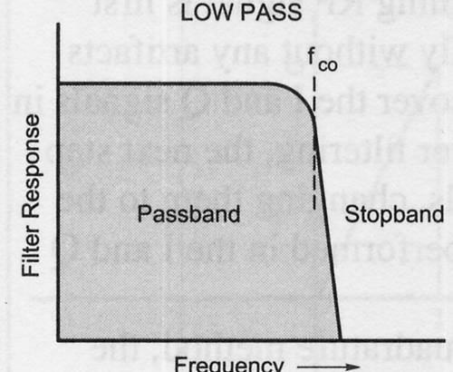
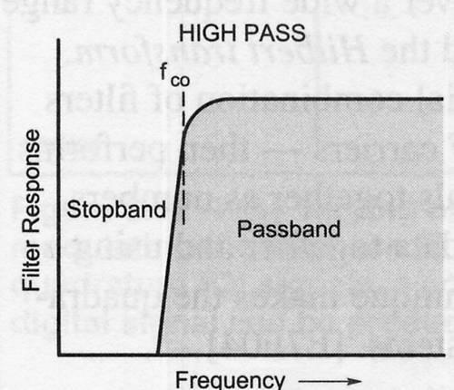
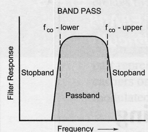
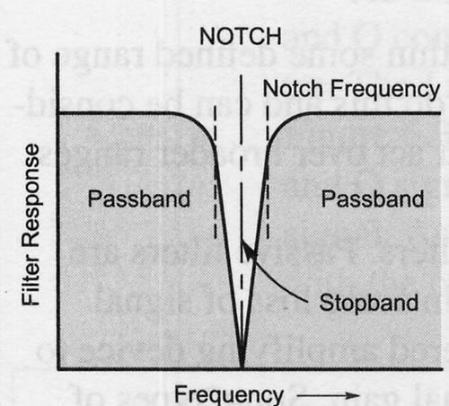
19 6.4 FILTERS AND IMPEDANCE MATCHING (page 6-35) FILTER FAMILIES AND RESPONSE TYPES (page 6-35) Passive filters are made with un-powered components (R-resistors, C-capacitors, L-inductors) and always results in some loss of signal strength called insertion loss. Active filters include a powered amplifying device to overcome the filter insertion loss and sometimes even provide signal gain. Mechanical filters are a class of passive filter that use internal elements such as disk and rods that vibrate at the frequencies of interest. Cavity filters are also a class of passive filter that uses the resonant characteristics of a conducting tube or box to act as a filter and are used in repeater duplexes because of their extremely low loss and sharp tuning characteristics. A cavity filter would be the best choice for use in a 2 meter repeater duplexer. Question E7C10: Which of the following filters would be the best choice for use in a 2 meter repeater duplexer? Answer: A cavity filter FILTER CLASSIFICATION (page 6-35) The Cutoff-frequency is the frequency at which the output signal power is one-half that of the input signal power. A Low-pass filter is one in which all frequencies below the cutoff-frequency are passed with little or no attenuation. A High-pass filter is one in which all frequencies above the cutoff-frequency are passed with little or no attenuation. A Band-pass filter has both an upper and lower cutoff frequency. Signals between the cutoff frequencies are passed, while those outside the passband are attenuated. A Band-stop filter has both an upper and lower cutoff frequency. Signals between the cutoff frequencies are attenuated, while those outside the cutoff frequencies are passed. This opposite reaction to the band-pass filter A Notch filter is a band-stop filter that has a very narrow frequency response. Wednesday, October 19,
20 BAND STOP Wednesday, October 19,
21 FILTER DESIGN (page 6-35) CHAPTER 6 Radio Circuits and Systems Ringing in a filter causes undesired oscillations added to the desired signal. Question E7G02: What is the effect of ringing in a filter? Answer: Undesired oscillations added to the desired signal Digital mode is most affected by non-linear phase response in a receiver IF filter. Question E7C14: Which mode is most affected by non-linear phase response in a receiver IF filter? Answer: Digital A Chebyshev filter is described as having ripple in the passband and a sharp cutoff. Question E7C05: Which filter type is described as having ripple in the passband and a sharp cutoff? Answer: A Chebyshev filter The distinguishing features of an elliptical filter is an extremely sharp cutoff with one or more notches in the stop band. Question E7C06: What are the distinguishing features of an elliptical filter? Answer: Extremely sharp cutoff with one or more notches in the stop band A notch filter would be used to attenuate an interfering carrier signal while receiving an SSB transmission. Question E7C07: What kind of filter would you use to attenuate an interfering carrier signal while receiving an SSB transmission? Answer: A notch filter CRYSTAL FILTERS (page 6-37) A crystal lattice filter is a filter with narrow bandwidth and steep skirts made using quartz crystals. Question E7C15: What is a crystal lattice filter? Answer: A filter with narrow bandwidth and steep skirts made using quartz crystals When building a crystal ladder filter remember that the relative frequencies of the individual crystals has the greatest effect in helping determine the bandwidth and response shape of a crystal ladder filter. Question E7C08: Which of the following factors has the greatest effect in helping determine the bandwidth and response shape of a crystal ladder filter? Answer: The relative frequencies of the individual crystals A Jones filter, as used as part of an HF receiver IF stage, is a variable bandwidth crystal lattice filter. Question E7C09: What is a Jones filter as used as part of an HF receiver IF stage? Answer: A variable bandwidth crystal lattice filter Wednesday, October 19,

22 ACTIVE FILTERS (page 6-38) ACTIVE AUDIO FILTERS (page 6-39) CHAPTER 6 Radio Circuits and Systems An audio filter in a receiver is the most appropriate use of an op-amp active filter. Question E7G06: Which of the following is the most appropriate use of an op-amp active filter? Answer: As an audio filter in a receiver By restricting both gain and Q we can eliminate unwanted ringing and audio instability in a multi-section op-amp RC audio filter circuit. Question E7G05: How can unwanted ringing and audio instability be prevented in a multi-section op-amp RC audio filter circuit? Answer: Restrict both gain and Q Shades of Star Trek. They are now making filters with biological products. Aplications: The Field Filters can be used in MmW and THz systems for filtering signal in transmission or reception. They are suitable for radio-communication, astronomy, material research or imaging applications. One of the most cutting-edge applications of Anteral s THz Filed Filters is biological and chemical sensing. Since the filters provide sharp peaks with high rejection at the resonant frequency, they can be used as sensing or detecting devices. By placing the element to be sensed on the surface, a redshift in the resonant frequency occurs which allows identifying the element. Anteral offers specific designs with superior sensitivity for sensing applications. Wednesday, October 19,
23 DIGITAL SIGNAL PROCESSING (DSP) filters (page 6-39) An Adaptive filter is used with a digital signal processing audio filter to remove unwanted noise from a received SSB signal. Question E7F02: What kind of digital signal processing audio filter is used to remove unwanted noise from a received SSB signal? Answer: An adaptive filter FINITE IMPULSE RESPONSE (FIR) FILTERS (page 6-40) The function of taps in a digital signal processing filter is that they Provide incremental signal delays for filter algorithms. Question E7F13: What is the function of taps in a digital signal processing filter? Answer: Provide incremental signal delays for filter algorithms More taps would allow a digital signal processing filter to create a sharper filter response. Question E7F14: Which of the following would allow a digital signal processing filter to create a sharper filter response? Answer: More taps INFINITE IMPULSE RESPONSE (IIR) FILTERS (page 6-41) (ERRATA: CORRECTION NEAR THE TOP OF PAGE 6-41) Unlike a symmetrical FIR filter, all frequency components of the input signal (in an IIR filter) are delayed by the same a different amount. So a FIR filters delay all frequency components of the signal by the same amount. Question E7F15: Which of the following is an advantage of a Finite Impulse Response (FIR) filter vs an Infinite Impulse Response (IIR) digital filter? Answer: FIR filters delay all frequency components of the signal by the same amount IMPEDANCE MATCHING (page 6-41) To perform the task of converting a complex impedance to a resistive impedance an impedance-matching circuit cancels the reactive part of the impedance and changes the resistive part to a desired value. Question E7C04: How does an impedance-matching circuit transform a complex impedance to a resistive impedance? Answer: It cancels the reactive part of the impedance and changes the resistive part to a desired value L-NETWORKS (page 6-42) Wednesday, October 19,
24 PI AND PI-L NETWORKS (page 6-42) CHAPTER 6 Radio Circuits and Systems The capacitors and inductors of a low-pass filter Pi-network are arranged between the network's input and output and ground to form a figure Pi. A capacitor is connected between the input and ground, another capacitor is connected between the output and ground, and an inductor is connected between input and output. Question E7C01: How are the capacitors and inductors of a low-pass filter Pi-network arranged between the network's input and output? Answer: A capacitor is connected between the input and ground, another capacitor is connected between the output and ground, and an inductor is connected between input and output The tuning capacitor is adjusted for minimum plate current, and the loading capacitor is adjusted for maximum permissible plate current. That is how the loading and tuning capacitors are to be adjusted when tuning a vacuum tube RF power amplifier that employs a Pi-network output circuit. Question E7B09: Which of the following describes how the loading and tuning capacitors are to be adjusted when tuning a vacuum tube RF power amplifier that employs a Pi-network output circuit? Answer: The tuning capacitor is adjusted for minimum plate current, and the loading capacitor is adjusted for maximum permissible plate current A Pi filter network is the common name for a filter network which is equivalent to two L-networks connected back-toback with the two inductors in series and the capacitors in shunt at the input and output. Question E7C11: Which of the following is the common name for a filter network which is equivalent to two L- networks connected back-to-back with the two inductors in series and the capacitors in shunt at the input and output? Answer: Pi One advantage of a Pi-matching network over an L-matching network consisting of a single inductor and a single capacitor is the Q of Pi-networks can be varied depending on the component values chosen. Question E7C13: What is one advantage of a Pi-matching network over an L-matching network consisting of a single inductor and a single capacitor? Answer: The Q of Pi-networks can be varied depending on the component values chosen A Pi-network with an additional series inductor on the output, which describes a Pi-L-network, is used for matching a vacuum tube final amplifier to a 50 ohm unbalanced output. Question E7C12: Which describes a Pi-L-network used for matching a vacuum tube final amplifier to a 50 ohm unbalanced output? Answer: A Pi-network with an additional series inductor on the output You get Greater harmonic suppression with a Pi-L-network over a regular Pi-network for impedance matching between the final amplifier of a vacuum-tube transmitter and an antenna. Question E7C03: What advantage does a Pi-L-network have over a regular Pi-network for impedance matching between the final amplifier of a vacuum-tube transmitter and an antenna? Answer: Greater harmonic suppression Wednesday, October 19,
25 T-NETWORKS (page 6-43) CHAPTER 6 Radio Circuits and Systems A T-network with series capacitors and a parallel shunt inductor makes a high-pass filter. Question E7C02: Which of the following is a property of a T-network with series capacitors and a parallel shunt inductor? Answer: It is a high-pass filter 6.5 POWER SUPPLIES (page 6-44) LINEAR VOLTAGE REGULATORS (page 6-44) One characteristic of a linear electronic voltage regulator is the conduction of a control element is varied to maintain a constant output voltage. Question E7D01: What is one characteristic of a linear electronic voltage regulator? Answer: The conduction of a control element is varied to maintain a constant output voltage SHUNT AND SERIES REGULATORS (page 6-44) A shunt regulator is a type of linear voltage regulator that places a constant load on the unregulated voltage source. Question E7D05: Which of the following types of linear voltage regulator places a constant load on the unregulated voltage source? Answer: A shunt regulator The pass transistor circuit element is controlled by a series analog voltage regulator to maintain a constant output voltage. Question E7D11: What circuit element is controlled by a series analog voltage regulator to maintain a constant output voltage? Answer: Pass transistor Figure E7-3 is a Linear voltage regulator. Question E7D08: What type of circuit is shown in Figure E7-3? Answer: Linear voltage regulator A Zener diode is typically used as a stable reference voltage in a linear voltage regulator. Figure E Q1 +12 C1 C3 R R2 Question E7D03: What device is typically used as a stable reference voltage in a linear voltage regulator? Answer: A Zener diode C D1 Wednesday, October 19,
26 The purpose of C2 in the circuit shown in Figure E7-3 is to bypasses hum around D1. Question E7D07: What is the purpose of C2 in the circuit shown in Figure E7-3? Answer: It bypasses hum around D1 Figure E Q1 +12 C1 C3 R R2 The purpose of Q1 in the circuit shown in Figure E7-3 is to increases the current-handling capability of the regulator. Question E7D06: What is the purpose of Q1 in the circuit shown in Figure E7-3? Answer: It increases the current-handling capability of the regulator C D1 IC THREE TERMINAL REGULATORS (page 6-45) EFFICIENCY AND POWER DISSIPATION (page 6-45) P DISS = (V IN V OUT ) I OUT Question E7D13: What is the equation for calculating power dissipation by a series connected linear voltage regulator? Answer: Voltage difference from input to output multiplied by output current A series (linear voltage) regulator usually makes the most efficient use of the primary power source. Question E7D04: Which of the following types of linear voltage regulator usually make the most efficient use of the primary power source? Answer: A series regulator The drop-out voltage of an analog voltage regulator is the minimum input-to-output voltage required to maintain regulation. Question E7D12: What is the drop-out voltage of an analog voltage regulator? Answer: Minimum input-to-output voltage required to maintain regulation BATTERY CHARGING REGULATORS (page 6-46) Prevention of battery damage due to overcharge is the main reason to use a charge controller with a solar power system. Question E7D09: What is the main reason to use a charge controller with a solar power system? Answer: Prevention of battery damage due to overcharge Wednesday, October 19,
27 SWITCHING REGULATORS (page 6-46) One characteristic of a switching electronic voltage regulator is that the controlled device s duty cycle is changed to produce a constant average output voltage. Question E7D02: What is one characteristic of a switching electronic voltage regulator? Answer: The controlled device s duty cycle is changed to produce a constant average output voltage The high frequency inverter design uses much smaller transformers and filter components for an equivalent power output and that is the primary reason that a high-frequency switching type high voltage power supply can be both less expensive and lighter in weight than a conventional power supply. Question E7D10: What is the primary reason that a high-frequency switching type high voltage power supply can be both less expensive and lighter in weight than a conventional power supply? Answer: The high frequency inverter design uses much smaller transformers and filter components for an equivalent power output HIGH VOLTAGE TECHNIQUES (page 6-46) CAPACITORS (page 6-46) When several electrolytic filter capacitors are connected in series to increase the operating voltage of a power supply filter circuit, resistors should be connected across each capacitor: To equalize, as much as possible, the voltage drop across each capacitor To provide a safety bleeder to discharge the capacitors when the supply is off To provide a minimum load current to reduce voltage excursions at light loads Question E7D16: When several electrolytic filter capacitors are connected in series to increase the operating voltage of a power supply filter circuit, why should resistors be connected across each capacitor? Answer: To equalize, as much as possible, the voltage drop across each capacitor Answer: To provide a safety bleeder to discharge the capacitors when the supply is off Answer: To provide a minimum load current to reduce voltage excursions at light loads Answer: All of these choices are correct The purpose of a "step-start" circuit in a high voltage power supply is to allow the filter capacitors to charge gradually. Question E7D15: What is the purpose of a "step-start" circuit in a high voltage power supply? Answer: To allow the filter capacitors to charge gradually Wednesday, October 19,


28 BLEEDER RESISTORS (page 6-47) CHAPTER 6 Radio Circuits and Systems Bleeder resistors provide protection against shock when the power supply is turned off and dangerous wiring is exposed because the bleed off : the stored charge in the filter capacitors. Bleed resistors are not only used in electronic equipment. Here is a picture of a bleed resistor in a motor start capacitor. A general rule is that the bleeder resistor should be designed to reduce the output voltage to 30 volts or less within 2 second of turning off the power supply. One purpose of a "bleeder" resistor in a conventional unregulated power supply is to improve output voltage regulation. Question E7D14: What is one purpose of a "bleeder" resistor in a conventional unregulated power supply? Answer: To improve output voltage regulation Wednesday, October 19,
7. Parameteric amplifiers are very low noise. They are common as the on-the-antenna amplifier of satellite signal receiver systems.
 Introduction Rather than try to give you the material so that you can answer the questions from first principles," I will provide enough information that you can recognize the correct answer to each question.
Introduction. Chapter 6 Notes
 Introduction Rather than try to give you the material so that you can answer the questions from first principles, I will provide enough information that you can recognize the correct answer to each question.
4/30/2012. General Class Element 3 Course Presentation. Practical Circuits. Practical Circuits. Subelement G7. 2 Exam Questions, 2 Groups
 General Class Element 3 Course Presentation ti ELEMENT 3 SUB ELEMENTS General Licensing Class Subelement G7 2 Exam Questions, 2 Groups G1 Commission s Rules G2 Operating Procedures G3 Radio Wave Propagation
EE301 ELECTRONIC CIRCUITS CHAPTER 2 : OSCILLATORS. Lecturer : Engr. Muhammad Muizz Bin Mohd Nawawi
 EE301 ELECTRONIC CIRCUITS CHAPTER 2 : OSCILLATORS Lecturer : Engr. Muhammad Muizz Bin Mohd Nawawi 2.1 INTRODUCTION An electronic circuit which is designed to generate a periodic waveform continuously at
PRACTICE. Amateur Radio Operator Certificate Examination. Advanced Qualification
 Innovation, Science and Economic Development Canada Innovation, Sciences et Développement économique Canada Amateur Radio Operator Certificate Examination Advanced Qualification 2018-06-30 To pass this
PRACTICE. Amateur Radio Operator Certificate Examination. Advanced Qualification
 Amateur Radio Operator ertificate Examination Advanced Qualification 2019-04-03 To pass this exam, you must correctly answer 35 out of 50 questions Exam Number: 115916 1. (A-007-008-002) Why would one
The steeper the phase shift as a function of frequency φ(ω) the more stable the frequency of oscillation
 the more stable the frequency of oscillation") It should be noted that the frequency of oscillation ω o is determined by the phase characteristics of the feedback loop. the loop oscillates at the frequency for which the phase is zero The steeper the
It should be noted that the frequency of oscillation ω o is determined by the phase characteristics of the feedback loop. the loop oscillates at the frequency for which the phase is zero The steeper the
MAHALAKSHMI ENGINEERING COLLEGE TIRUCHIRAPALLI UNIT III TUNED AMPLIFIERS PART A (2 Marks)
") MAHALAKSHMI ENGINEERING COLLEGE TIRUCHIRAPALLI-621213. UNIT III TUNED AMPLIFIERS PART A (2 Marks) 1. What is meant by tuned amplifiers? Tuned amplifiers are amplifiers that are designed to reject a certain
MAHALAKSHMI ENGINEERING COLLEGE TIRUCHIRAPALLI-621213. UNIT III TUNED AMPLIFIERS PART A (2 Marks) 1. What is meant by tuned amplifiers? Tuned amplifiers are amplifiers that are designed to reject a certain
HF Receivers, Part 2
 HF Receivers, Part 2 Superhet building blocks: AM, SSB/CW, FM receivers Adam Farson VA7OJ View an excellent tutorial on receivers NSARC HF Operators HF Receivers 2 1 The RF Amplifier (Preamp)! Typical
Power Amplifiers. Class A Amplifier
 Power Amplifiers The Power amplifiers amplify the power level of the signal. This amplification is done in the last stage in audio applications. The applications related to radio frequencies employ radio
Table of Contents Lesson One Lesson Two Lesson Three Lesson Four Lesson Five PREVIEW COPY
 Oscillators Table of Contents Lesson One Lesson Two Lesson Three Introduction to Oscillators...3 Flip-Flops...19 Logic Clocks...37 Lesson Four Filters and Waveforms...53 Lesson Five Troubleshooting Oscillators...69
General Class License Theory II. Dick Grote K6PBF
 General Class License Theory II Dick Grote K6PBF k6pbfdick@gmail.com 1 Introduction In the first theory class we talked about basic electrical principles and components. Now we will build on this to learn
Technician License Course Chapter 3 Types of Radios and Radio Circuits. Module 7
 Technician License Course Chapter 3 Types of Radios and Radio Circuits Module 7 Radio Block Diagrams Radio Circuits can be shown as functional blocks connected together. Knowing the description of common
Chapter 6: Power Amplifiers
 Chapter 6: Power Amplifiers Contents Class A Class B Class C Power Amplifiers Class A, B and C amplifiers are used in transmitters Tuned with a band width wide enough to pass all information sidebands
UNIT-3. Electronic Measurements & Instrumentation
 UNIT-3 1. Draw the Block Schematic of AF Wave analyzer and explain its principle and Working? ANS: The wave analyzer consists of a very narrow pass-band filter section which can Be tuned to a particular
KWM-2/2A Transceiver THE COLLINS KWM-2/2A TRANSCEIVER
 KWM-2/2A Transceiver Click the photo to see a larger photo Click "Back" button on browser to return Courtesy of Norm - WA3KEY THE COLLINS KWM-2/2A TRANSCEIVER Unmatched for versatility, dependability and
Introduction Introduction to radio frequencies p. 3 What are the 'radio frequencies'? p. 3 Why are radio frequencies different? p.
 Foreword p. xi Preface p. xiii Introduction Introduction to radio frequencies p. 3 What are the 'radio frequencies'? p. 3 Why are radio frequencies different? p. 3 What this book covers p. 3 Signals and
Basic Operational Amplifier Circuits
 Basic Operational Amplifier Circuits Comparators A comparator is a specialized nonlinear op-amp circuit that compares two input voltages and produces an output state that indicates which one is greater.
The G4EGQ RAE COURSE Lesson 9 Transmitters Lesson 8 looked at a simple transmitter exciter comprising of oscillator, buffer and multiplier stages.
 Lesson 8 looked at a simple transmitter exciter comprising of oscillator, buffer and multiplier stages. The power amplifier The output from the exciter is usually very low and it is necessary to amplify
Chapter 13 Oscillators and Data Converters
 Chapter 13 Oscillators and Data Converters 13.1 General Considerations 13.2 Ring Oscillators 13.3 LC Oscillators 13.4 Phase Shift Oscillator 13.5 Wien-Bridge Oscillator 13.6 Crystal Oscillators 13.7 Chapter
LINEAR IC APPLICATIONS
 1 B.Tech III Year I Semester (R09) Regular & Supplementary Examinations December/January 2013/14 1 (a) Why is R e in an emitter-coupled differential amplifier replaced by a constant current source? (b)
Chapter 2. The Fundamentals of Electronics: A Review
 Chapter 2 The Fundamentals of Electronics: A Review Topics Covered 2-1: Gain, Attenuation, and Decibels 2-2: Tuned Circuits 2-3: Filters 2-4: Fourier Theory 2-1: Gain, Attenuation, and Decibels Most circuits
Oscillators. An oscillator may be described as a source of alternating voltage. It is different than amplifier.
 Oscillators An oscillator may be described as a source of alternating voltage. It is different than amplifier. An amplifier delivers an output signal whose waveform corresponds to the input signal but
Receiver Architecture
 Receiver Architecture Receiver basics Channel selection why not at RF? BPF first or LNA first? Direct digitization of RF signal Receiver architectures Sub-sampling receiver noise problem Heterodyne receiver
Radio Receivers. Al Penney VO1NO
 Radio Receivers Al Penney VO1NO Role of the Receiver The Antenna must capture the radio wave. The desired frequency must be selected from all the EM waves captured by the antenna. The selected signal is
LBI-30398N. MAINTENANCE MANUAL MHz PHASE LOCK LOOP EXCITER 19D423249G1 & G2 DESCRIPTION TABLE OF CONTENTS. Page. DESCRIPTION...
 MAINTENANCE MANUAL 138-174 MHz PHASE LOCK LOOP EXCITER 19D423249G1 & G2 LBI-30398N TABLE OF CONTENTS DESCRIPTION...Front Cover CIRCUIT ANALYSIS... 1 MODIFICATION INSTRUCTIONS... 4 PARTS LIST AND PRODUCTION
1. What is the unit of electromotive force? (a) volt (b) ampere (c) watt (d) ohm. 2. The resonant frequency of a tuned (LRC) circuit is given by
 volt (b) ampere (c) watt (d) ohm. 2. The resonant frequency of a tuned (LRC) circuit is given by") Department of Examinations, Sri Lanka EXAMINATION FOR THE AMATEUR RADIO OPERATORS CERTIFICATE OF PROFICIENCY ISSUED BY THE DIRECTOR GENERAL OF TELECOMMUNICATIONS, SRI LANKA 2004 (NOVICE CLASS) Basic Electricity,
Department of Examinations, Sri Lanka EXAMINATION FOR THE AMATEUR RADIO OPERATORS CERTIFICATE OF PROFICIENCY ISSUED BY THE DIRECTOR GENERAL OF TELECOMMUNICATIONS, SRI LANKA 2004 (NOVICE CLASS) Basic Electricity,
Operational Amplifiers
 Operational Amplifiers Table of contents 1. Design 1.1. The Differential Amplifier 1.2. Level Shifter 1.3. Power Amplifier 2. Characteristics 3. The Opamp without NFB 4. Linear Amplifiers 4.1. The Non-Inverting
Gechstudentszone.wordpress.com
 8.1 Operational Amplifier (Op-Amp) UNIT 8: Operational Amplifier An operational amplifier ("op-amp") is a DC-coupled high-gain electronic voltage amplifier with a differential input and, usually, a single-ended
TUNED AMPLIFIERS 5.1 Introduction: Coil Losses:
 TUNED AMPLIFIERS 5.1 Introduction: To amplify the selective range of frequencies, the resistive load R C is replaced by a tuned circuit. The tuned circuit is capable of amplifying a signal over a narrow
OBJECTIVE TYPE QUESTIONS
 OBJECTIVE TYPE QUESTIONS Q.1 The breakdown mechanism in a lightly doped p-n junction under reverse biased condition is called (A) avalanche breakdown. (B) zener breakdown. (C) breakdown by tunnelling.
ERICSSONZ LBI-30398P. MAINTENANCE MANUAL MHz PHASE LOCKED LOOP EXCITER 19D423249G1 & G2 DESCRIPTION TABLE OF CONTENTS
 MAINTENANCE MANUAL 138-174 MHz PHASE LOCKED LOOP EXCITER 19D423249G1 & G2 TABLE OF CONTENTS Page DESCRIPTION... Front Cover CIRCUIT ANALYSIS...1 MODIFICATION INSTRUCTIONS...4 PARTS LIST...5 PRODUCTION
f o Fig ECE 6440 Frequency Synthesizers P.E. Allen Frequency Magnitude Spectral impurity Frequency Fig010-03
 Lecture 010 Introduction to Synthesizers (5/5/03) Page 010-1 LECTURE 010 INTRODUCTION TO FREQUENCY SYNTHESIZERS (References: [1,5,9,10]) What is a Synthesizer? A frequency synthesizer is the means by which
Glossary of VCO terms
 Glossary of VCO terms VOLTAGE CONTROLLED OSCILLATOR (VCO): This is an oscillator designed so the output frequency can be changed by applying a voltage to its control port or tuning port. FREQUENCY TUNING
An active filter offers the following advantages over a passive filter:
 ACTIVE FILTERS An electric filter is often a frequency-selective circuit that passes a specified band of frequencies and blocks or attenuates signals of frequencies outside this band. Filters may be classified
Communication Circuit Lab Manual
 German Jordanian University School of Electrical Engineering and IT Department of Electrical and Communication Engineering Communication Circuit Lab Manual Experiment 3 Crystal Oscillator Eng. Anas Alashqar
AM Generation High Level Low Level
 AM Generation High Level Low Level Low-level generation In modern radio systems, modulated signals are generated via digital signal processing (DSP). With DSP many types of AM modulation are possible with
B.Tech II Year II Semester (R13) Supplementary Examinations May/June 2017 ANALOG COMMUNICATION SYSTEMS (Electronics and Communication Engineering)
 Supplementary Examinations May/June 2017 ANALOG COMMUNICATION SYSTEMS (Electronics and Communication Engineering)") Code: 13A04404 R13 B.Tech II Year II Semester (R13) Supplementary Examinations May/June 2017 ANALOG COMMUNICATION SYSTEMS (Electronics and Communication Engineering) Time: 3 hours Max. Marks: 70 PART A
Code: 13A04404 R13 B.Tech II Year II Semester (R13) Supplementary Examinations May/June 2017 ANALOG COMMUNICATION SYSTEMS (Electronics and Communication Engineering) Time: 3 hours Max. Marks: 70 PART A
Chapter.8: Oscillators
 Chapter.8: Oscillators Objectives: To understand The basic operation of an Oscillator the working of low frequency oscillators RC phase shift oscillator Wien bridge Oscillator the working of tuned oscillator
Radio Receivers. Al Penney VO1NO
 Radio Receivers Role of the Receiver The Antenna must capture the radio wave. The desired frequency must be selected from all the EM waves captured by the antenna. The selected signal is usually very weak
DIGITAL ELECTRONICS WAVE SHAPING AND PULSE CIRCUITS. September 2012
 AM 5-403 DIGITAL ELECTRONICS WAVE SHAPING AND PULSE CIRCUITS September 2012 DISTRIBUTION RESTRICTION: Approved for public release. Distribution is unlimited. DEPARTMENT OF THE ARMY MILITARY AUXILIARY RADIO
EE12: Laboratory Project (Part-2) AM Transmitter
 AM Transmitter") EE12: Laboratory Project (Part-2) AM Transmitter ECE Department, Tufts University Spring 2008 1 Objective This laboratory exercise is the second part of the EE12 project of building an AM transmitter in
EE12: Laboratory Project (Part-2) AM Transmitter ECE Department, Tufts University Spring 2008 1 Objective This laboratory exercise is the second part of the EE12 project of building an AM transmitter in
Chapter 6. FM Circuits
 Chapter 6 FM Circuits Topics Covered 6-1: Frequency Modulators 6-2: Frequency Demodulators Objectives You should be able to: Explain the operation of an FM modulators and demodulators. Compare and contrast;
Interference & Suppression Page 59
 INTERFERENCE Interference & Suppression Page 59 Front-End Overload, Cross-Modulation What is meant by receiver overload? Interference caused by strong signals from a nearby transmitter What is one way
Receiver Design. Prof. Tzong-Lin Wu EMC Laboratory Department of Electrical Engineering National Taiwan University 2011/2/21
 Receiver Design Prof. Tzong-Lin Wu EMC Laboratory Department of Electrical Engineering National Taiwan University 2011/2/21 MW & RF Design / Prof. T. -L. Wu 1 The receiver mush be very sensitive to -110dBm
Code: 9A Answer any FIVE questions All questions carry equal marks *****
 II B. Tech II Semester (R09) Regular & Supplementary Examinations, April/May 2012 ELECTRONIC CIRCUIT ANALYSIS (Common to EIE, E. Con. E & ECE) Time: 3 hours Max Marks: 70 Answer any FIVE questions All
Figure 12-1 (p. 578) Block diagram of a sinusoidal oscillator using an amplifier with a frequencydependent
 Block diagram of a sinusoidal oscillator using an amplifier with a frequencydependent") Figure 12-1 (p. 578) Block diagram of a sinusoidal oscillator using an amplifier with a frequencydependent feedback path. Figure 12-2 (p. 579) General circuit for a transistor oscillator. The transistor
Figure 12-1 (p. 578) Block diagram of a sinusoidal oscillator using an amplifier with a frequencydependent feedback path. Figure 12-2 (p. 579) General circuit for a transistor oscillator. The transistor
Crystal Oscillators and Circuits
 Crystal Oscillators and Circuits It is often required to produce a signal whose frequency or pulse rate is very stable and exactly known. This is important in any application where anything to do with
LM125 Precision Dual Tracking Regulator
 LM125 Precision Dual Tracking Regulator INTRODUCTION The LM125 is a precision, dual, tracking, monolithic voltage regulator. It provides separate positive and negative regulated outputs, thus simplifying
About the Tutorial. Audience. Prerequisites. Copyright & Disclaimer. Linear Integrated Circuits Applications
 About the Tutorial Linear Integrated Circuits are solid state analog devices that can operate over a continuous range of input signals. Theoretically, they are characterized by an infinite number of operating
EC202- ELECTRONIC CIRCUITS II Unit- I -FEEEDBACK AMPLIFIER
 EC202- ELECTRONIC CIRCUITS II Unit- I -FEEEDBACK AMPLIFIER 1. What is feedback? What are the types of feedback? 2. Define positive feedback. What are its merits and demerits? 3. Define negative feedback.
High Frequency VCO Design and Schematics
 High Frequency VCO Design and Schematics Iulian Rosu, YO3DAC / VA3IUL, http://www.qsl.net/va3iul/ This note will review the process by which VCO (Voltage Controlled Oscillator) designers choose their oscillator
Analog I/O. ECE 153B Sensor & Peripheral Interface Design Winter 2016
 Analog I/O ECE 153B Sensor & Peripheral Interface Design Introduction Anytime we need to monitor or control analog signals with a digital system, we require analogto-digital (ADC) and digital-to-analog
TONE DECODER / PHASE LOCKED LOOP PIN FUNCTION 1 OUTPUT FILTER 2 LOW-PASS FILTER 3 INPUT 4 V + 5 TIMING R 6 TIMING CR 7 GROUND 8 OUTPUT
 TONE DECODER / PHASE LOCKED LOOP GENERAL DESCRIPTION The NJM567 tone and frequency decoder is a highly stable phase locked loop with synchronous AM lock detection and power output circuitry. Its primary
Experiment No. 2 Pre-Lab Signal Mixing and Amplitude Modulation
 Experiment No. 2 Pre-Lab Signal Mixing and Amplitude Modulation Read the information presented in this pre-lab and answer the questions given. Submit the answers to your lab instructor before the experimental
Master Degree in Electronic Engineering
 Master Degree in Electronic Engineering Analog and telecommunication electronic course (ATLCE-01NWM) Miniproject: Baseband signal transmission techniques Name: LI. XINRUI E-mail: s219989@studenti.polito.it
UNIT 2. Q.1) Describe the functioning of standard signal generator. Ans. Electronic Measurements & Instrumentation
 Describe the functioning of standard signal generator. Ans. Electronic Measurements & Instrumentation") UNIT 2 Q.1) Describe the functioning of standard signal generator Ans. STANDARD SIGNAL GENERATOR A standard signal generator produces known and controllable voltages. It is used as power source for the
UNIT 2 Q.1) Describe the functioning of standard signal generator Ans. STANDARD SIGNAL GENERATOR A standard signal generator produces known and controllable voltages. It is used as power source for the
Question Paper Code: 21398
 Reg. No. : Question Paper Code: 21398 B.E./B.Tech. DEGREE EXAMINATION, MAY/JUNE 2013 Fourth Semester Electrical and Electronics Engineering EE2254 LINEAR INTEGRATED CIRCUITS AND APPLICATIONS (Regulation
Modulation Methods Frequency Modulation
 Modulation Methods Frequency Modulation William Sheets K2MQJ Rudolf F. Graf KA2CWL The use of frequency modulation (called FM) is another method of adding intelligence to a carrier signal. While simple
EVALUATION KIT AVAILABLE 10MHz to 1050MHz Integrated RF Oscillator with Buffered Outputs. Typical Operating Circuit. 10nH 1000pF MAX2620 BIAS SUPPLY
 19-1248; Rev 1; 5/98 EVALUATION KIT AVAILABLE 10MHz to 1050MHz Integrated General Description The combines a low-noise oscillator with two output buffers in a low-cost, plastic surface-mount, ultra-small
Glossary + - A BNC plug that shorts the inner wire in a coax cable to the outer shield through a
 50Ω Terminator AC Active Alligator Clip Back Bias Base Battery Bias + - Bipolar Transistor BJT Black Box BNC BNC Cable A BNC plug that shorts the inner wire in a coax cable to the outer shield through
Code No: R Set No. 1
 Code No: R05220405 Set No. 1 II B.Tech II Semester Regular Examinations, Apr/May 2007 ANALOG COMMUNICATIONS ( Common to Electronics & Communication Engineering and Electronics & Telematics) Time: 3 hours
MAHARASHTRA STATE BOARD OF TECHNICAL EDUCATION (Autonomous) (ISO/IEC Certified) Summer 2016 EXAMINATIONS.
 (ISO/IEC Certified) Summer 2016 EXAMINATIONS.") Summer 2016 EXAMINATIONS Subject Code: 17321 Model Answer Important Instructions to examiners: 1) The answers should be examined by key words and not as word-to-word as given in the answer scheme. 2) The
Summer 2016 EXAMINATIONS Subject Code: 17321 Model Answer Important Instructions to examiners: 1) The answers should be examined by key words and not as word-to-word as given in the answer scheme. 2) The
RADIO RECEIVERS ECE 3103 WIRELESS COMMUNICATION SYSTEMS
 RADIO RECEIVERS ECE 3103 WIRELESS COMMUNICATION SYSTEMS FUNCTIONS OF A RADIO RECEIVER The main functions of a radio receiver are: 1. To intercept the RF signal by using the receiver antenna 2. Select the
Chapter 2 Analog-to-Digital Conversion...
 Chapter... 5 This chapter examines general considerations for analog-to-digital converter (ADC) measurements. Discussed are the four basic ADC types, providing a general description of each while comparing
Norfolk Amateur Radio Club
 Norfolk Amateur Radio Club The Transmitter & Transmitter Interference Nick M0HGU & Steve G3PND Plan for the Day The Transmitter Introduction, Block diagrams Oscillators, Buffers & Multipliers Modulation
VCO Design Project ECE218B Winter 2011
 VCO Design Project ECE218B Winter 2011 Report due 2/18/2011 VCO DESIGN GOALS. Design, build, and test a voltage-controlled oscillator (VCO). 1. Design VCO for highest center frequency (< 400 MHz). 2. At
GLOSSARY. A connector used to T together two BNC coax cables and a BNC jack. The transfer function vs. frequency plotted on Log Log axis.
 GLOSSARY 50ΩTerminator AC Active Alligator Clip Back Bias Base Battery Bias + - Bipolar Transistor BJT Black Box BNC BNC Cable A BNC plug that shorts the inner wire in a coax cable to the outer shield
Summer 2015 Examination
 Summer 2015 Examination Subject Code: 17445 Model Answer Important Instructions to examiners: 1) The answers should be examined by key words and not as word-to-word as given in the model answer scheme.
Technical Article A DIRECT QUADRATURE MODULATOR IC FOR 0.9 TO 2.5 GHZ WIRELESS SYSTEMS
 Introduction As wireless system designs have moved from carrier frequencies at approximately 9 MHz to wider bandwidth applications like Personal Communication System (PCS) phones at 1.8 GHz and wireless
D-STATE RADIOMETER. I. Switch Driver
 NATIONAL RADIO ASTRONOMY OBSERVATORY Green Bank, West Virginia Electronics Division Internal Report No. 13 A SOLID-STATE RADIOMETER James L. Dolan August 1963 Rerun 11/10/ 66: 50 D-STATE RADIOMETER Work
6.776 High Speed Communication Circuits and Systems Lecture 14 Voltage Controlled Oscillators
 6.776 High Speed Communication Circuits and Systems Lecture 14 Voltage Controlled Oscillators Massachusetts Institute of Technology March 29, 2005 Copyright 2005 by Michael H. Perrott VCO Design for Narrowband
Feedback Amplifier & Oscillators
 256 UNIT 5 Feedback Amplifier & Oscillators 5.1 Learning Objectives Study definations of positive /negative feedback. Study the camparions of positive and negative feedback. Study the block diagram and
Low Distortion Mixer AD831
 a FEATURES Doubly-Balanced Mixer Low Distortion +2 dbm Third Order Intercept (IP3) + dbm 1 db Compression Point Low LO Drive Required: dbm Bandwidth MHz RF and LO Input Bandwidths 2 MHz Differential Current
Amateur Radio Examination EXAMINATION PAPER No. 275 MARKER S COPY
 01-6-(d) An Amateur Station is quoted in the regulations as a station: a for training new radio operators b using amateur equipment for commercial purposes c for public emergency purposes d in the Amateur
HF Receivers, Part 3
 HF Receivers, Part 3 Introduction to frequency synthesis; ancillary receiver functions Adam Farson VA7OJ View an excellent tutorial on receivers Another link to receiver principles NSARC HF Operators HF
Let us consider the following block diagram of a feedback amplifier with input voltage feedback fraction,, be positive i.e. in phase.
 P a g e 2 Contents 1) Oscillators 3 Sinusoidal Oscillators Phase Shift Oscillators 4 Wien Bridge Oscillators 4 Square Wave Generator 5 Triangular Wave Generator Using Square Wave Generator 6 Using Comparator
DHANALAKSHMI COLLEGE OF ENGINEERING DEPARTMENT OF ELECTRICAL AND ELECTRONICS ENGINEERING EC6202 ELECTRONIC DEVICES AND CIRCUITS
 DHANALAKSHMI COLLEGE OF ENGINEERING DEPARTMENT OF ELECTRICAL AND ELECTRONICS ENGINEERING EC6202 ELECTRONIC DEVICES AND CIRCUITS UNIT-I - PN DIODEAND ITSAPPLICATIONS 1. What is depletion region in PN junction?
WINTER 14 EXAMINATION. Model Answer. 1) The answers should be examined by key words and not as word-to-word as given in the
 The answers should be examined by key words and not as word-to-word as given in the") WINTER 14 EXAMINATION Subject Code: 17213 Model Answer Important Instructions to examiners: 1) The answers should be examined by key words and not as word-to-word as given in the model answer scheme. 2)
WINTER 14 EXAMINATION Subject Code: 17213 Model Answer Important Instructions to examiners: 1) The answers should be examined by key words and not as word-to-word as given in the model answer scheme. 2)
Analog Filter and. Circuit Design Handbook. Arthur B. Williams. Singapore Sydney Toronto. Mc Graw Hill Education
 Analog Filter and Circuit Design Handbook Arthur B. Williams Mc Graw Hill Education New York Chicago San Francisco Athens London Madrid Mexico City Milan New Delhi Singapore Sydney Toronto Contents Preface
UNIVERSITY OF NORTH CAROLINA AT CHARLOTTE Department of Electrical and Computer Engineering
 UNIVERSITY OF NORTH CAROLINA AT CHARLOTTE Department of Electrical and Computer Engineering EXPERIMENT 8 AMPLITUDE MODULATION AND DEMODULATION OBJECTIVES The focus of this lab is to familiarize the student
note application Measurement of Frequency Stability and Phase Noise by David Owen
 application Measurement of Frequency Stability and Phase Noise note by David Owen The stability of an RF source is often a critical parameter for many applications. Performance varies considerably with
ELC224 Final Review (12/10/2009) Name:
 Name:") ELC224 Final Review (12/10/2009) Name: Select the correct answer to the problems 1 through 20. 1. A common-emitter amplifier that uses direct coupling is an example of a dc amplifier. 2. The frequency
ELC224 Final Review (12/10/2009) Name: Select the correct answer to the problems 1 through 20. 1. A common-emitter amplifier that uses direct coupling is an example of a dc amplifier. 2. The frequency
Session 3. CMOS RF IC Design Principles
 Session 3 CMOS RF IC Design Principles Session Delivered by: D. Varun 1 Session Topics Standards RF wireless communications Multi standard RF transceivers RF front end architectures Frequency down conversion
FREQUENTLY ASKED QUESTIONS
 FREQUENTLY ASKED QUESTIONS UNIT-1 SUBJECT : ELECTRONIC DEVICES AND CIRCUITS SUBJECT CODE : EC6202 BRANCH: EEE PART -A 1. What is meant by diffusion current in a semi conductor? (APR/MAY 2010, 2011, NOV/DEC
GOVERNMENT OF KARNATAKA KARNATAKA STATE PRE-UNIVERSITY EDUCATION EXAMINATION BOARD II YEAR PUC EXAMINATION JULY-2012 SCHEME OF VALUATION
 GOVERNMENT OF KARNATAKA KARNATAKA STATE PRE-UNIVERSITY EDUCATION EXAMINATION BOARD II YEAR PUC EXAMINATION JULY-0 SCHEME OF VALUATION Subject Code: 40 Subject: PART - A 0. Which region of the transistor
4/29/2012. General Class Element 3 Course Presentation. Signals and Emissions. SignalSignals and Emissionsissions. Subelement G8
 General Class Element 3 Course Presentation ti ELEMENT 3 SUB ELEMENTS General Licensing Class Subelement G8 Signals and Emissions 2 Exam Questions, 2 Groups G1 Commission s Rules G2 Operating Procedures
High Frequency VCO Design and Schematics
 High Frequency VCO Design and Schematics Iulian Rosu, YO3DAC / VA3IUL, http://www.qsl.net/va3iul/ This note will review the process by which VCO (Voltage Controlled Oscillator) designers choose their oscillator
Common-emitter amplifier, no feedback, with reference waveforms for comparison.
 Feedback If some percentage of an amplifier's output signal is connected to the input, so that the amplifier amplifies part of its own output signal, we have what is known as feedback. Feedback comes in
Charan Langton, Editor
 Charan Langton, Editor SIGNAL PROCESSING & SIMULATION NEWSLETTER Baseband, Passband Signals and Amplitude Modulation The most salient feature of information signals is that they are generally low frequency.
Op Amp Booster Designs
 Op Amp Booster Designs Although modern integrated circuit operational amplifiers ease linear circuit design, IC processing limits amplifier output power. Many applications, however, require substantially
onlinecomponents.com FET Circuit Applications FET Circuit Applications AN-32 National Semiconductor Application Note 32 February 1970
 FET Circuit Applications National Semiconductor Application Note 32 February 1970 Polycarbonate dielectric Sample and Hold With Offset Adjustment TL H 6791 1 Long Time Comparator TL H 6791 2 The 2N4393
Unit/Standard Number. LEA Task # Alignment
 1 Secondary Competency Task List 100 SAFETY 101 Demonstrate an understanding of State and School safety regulations. 102 Practice safety techniques for electronics work. 103 Demonstrate an understanding
RF Components and Circuits
 RF Components and Circuits RF Components and Circuits Joseph J. Carr Newnes OXFORD AMSTERDAM BOSTON LONDON NEW YORK PARIS SAN DIEGO SAN FRANCISCO SINGAPORE SYDNEY TOKYO Newnes An imprint of Elsevier Science
FSK DEMODULATOR / TONE DECODER
 FSK DEMODULATOR / TONE DECODER GENERAL DESCRIPTION The is a monolithic phase-locked loop (PLL) system especially designed for data communications. It is particularly well suited for FSK modem applications,
UNIT V - RECTIFIERS AND POWER SUPPLIES
 UNIT V - RECTIFIERS AND POWER SUPPLIES OBJECTIVE On the completion of this unit the student will understand CLASSIFICATION OF POWER SUPPLY HALF WAVE, FULL WAVE, BRIDGE RECTIFER AND ITS RIPPLE FACTOR C,
G5A07 (D) What happens when the impedance of an electrical load is equal to the internal impedance of the power source?
 What happens when the impedance of an electrical load is equal to the internal impedance of the power source?") G5A07 (D) What happens when the impedance of an electrical load is equal to the internal impedance of the power source? A. The source delivers minimum power to the load B. The electrical load is shorted
G5A07 (D) What happens when the impedance of an electrical load is equal to the internal impedance of the power source? A. The source delivers minimum power to the load B. The electrical load is shorted
GATE: Electronics MCQs (Practice Test 1 of 13)
") GATE: Electronics MCQs (Practice Test 1 of 13) 1. Removing bypass capacitor across the emitter leg resistor in a CE amplifier causes a. increase in current gain b. decrease in current gain c. increase
GATE: Electronics MCQs (Practice Test 1 of 13) 1. Removing bypass capacitor across the emitter leg resistor in a CE amplifier causes a. increase in current gain b. decrease in current gain c. increase
UNIVERSITY OF UTAH ELECTRICAL ENGINEERING DEPARTMENT
 UNIVERSITY OF UTAH ELECTRICAL ENGINEERING DEPARTMENT ECE 3110 LAB EXPERIMENT NO. 4 CLASS AB POWER OUTPUT STAGE Objective: In this laboratory exercise you will build and characterize a class AB power output
3 Circuit Theory. 3.2 Balanced Gain Stage (BGS) Input to the amplifier is balanced. The shield is isolated
 Input to the amplifier is balanced. The shield is isolated") Rev. D CE Series Power Amplifier Service Manual 3 Circuit Theory 3.0 Overview This section of the manual explains the general operation of the CE power amplifier. Topics covered include Front End Operation,
Rev. D CE Series Power Amplifier Service Manual 3 Circuit Theory 3.0 Overview This section of the manual explains the general operation of the CE power amplifier. Topics covered include Front End Operation,