Section 2.3 Bipolar junction transistors - BJTs
|
|
|
- Lynn Mills
- 6 years ago
- Views:
Transcription
1 Section 2.3 Bipolar junction transistors - BJTs Single junction devices, such as p-n and Schottkty diodes can be used to obtain rectifying I-V characteristics, and to form electronic switching circuits The transferred-resistance or transistor is a multijunction device that is capable of Current gain Voltage gain Signal-power gain The transistor is therefore referred to as an active device, where-as the diode is passive Basic action - control of I at one terminal by a voltage applied across two other terminals
2 There are three major types of transistor Bipolar junction transistor or BJT Metal-oxide field effect transistor or MOSFET Junction FET or JFET In this case we will consider the first two, as they account for the vast majority of silicon devices produced today The BJT has three separately doped regions and two p-n junctions, which are sufficiently close together that they interact with each other. In this sense a BJT must NOT be considered as two back-to-back diodes. The BJT is a voltage-controlled current source. We will consider the various factors that determine the current gain, and the limitations imposed by real device characteristics.

3 BJT structure - three regions, two p-n junctions, three terminals (emitter, base, collector) Devices can be p-n-p, or n-p-n structures Width of the base is small compared to the minority carrier length Emitter is normally heavily doped, the collector has light doping The concepts you learnt earlier for p-n junctions are going to be built upon here - if you are not happy with these you must revise them now

4 These schematic representations are useful for analysing the basic operation of the structure. However, real devices are not symmetrical, and we will consider the impact of this on device operation later Real devices look more like this; conventional device (left), oxide-isolated device (right)
5 Principle of operation Consider an npn device - pnp devices behave similarly Assume an idealised structure such as that below - uniform and even doping First let us consider operation in the forward-active mode: B-E junction is forward biased so electrons can be injected from the emitter to the base, B-C junction is reverse biased.
6 Under these conditions we can expect Large concentration of minority carriers to appear in the base near the B-E junction, due to injection of electrons from the emitter A concentration gradient will be created within the base region in terms of minority carriers; this will generate a diffusion current through the base The B-C junction is reverse biased, so majority carriers (holes) from the base do not enter the collector in large concentrations; however, the minority carriers that diffuse to the B-C junction will be readily swept across If the base region is very narrow, comparable to electron diffusion lengths, few electrons will be lost through recombination and a collector current will be measured
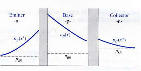
7 The MINORITY carrier concentrations will look like -

8 The number of electrons per unit time reaching the collector is proportional to the number of electrons injected into the base. The number of injected electrons is a function of the B-E voltage. To a first approx. the collector current is independent of the reverse biased B-C voltage - thus, the device looks like a constant current source.
9 The collector current is being controlled by the B-E voltage, or the current in the one part of the device is being controlled by the voltage in another part - transistor action Since the B-E junction is forward biased, holes from the base are injected into the emitter. However, these injected holes do not contribute to the collector current and are therefore not part of the transistor action To design a useful device, we need mathematical expressions for the minority carrier concentrations shown in the figure above. There are three modes of operation we must consider Forward-active (B-E FB, B-C RB) Cut-off (B-E RB, B-C RB) Saturation (B-E FB, B-C FB)
10 Npn transistor in a simple circuit, known as common-emitter

11 To calculate the currents in the BJT we must consider minority carrier transport, as we did with the p-n junction diode The table on the next slide shows the notation we are going to use in this analysis Consider a uniformly doped npn transistor in the forward active mode of operation
12

13 In the forward active mode, the minority carrier concentrations will appear as
14 The functions p E (x ), n B (x) and p C (x ) denote the steady state minority carrier concentrations in the emitter, base and collector respectively Assume that the neutral collector length x C is long Compared to the minority carrier diffusion length L C in the Collector, but we will take into account a finite emitter Length x E Assume that the surface recombination velocity at x = x E is Infinite, then the excess minority carrier concentration at X = x E is zero, or p E (x = x E ) = p E0 An infinite surface recombination velocity is a good approx. when an ohmic contact is fabricated at x = x E We are now ready to analyse the current flows expected in each region of the transistor, and hence be able to model its behaviour during operation
15 Base region We need to use the ambipolar transport equation, for a zero electric field in the neutral base region, this equation reduces to Where n B is the excess minority carrier electron concentration and D B and B0 are the minority carrier diffusion coefficent and lifetime in the base region respectively The excess electron concentration is defined as
16 The general solution to the transport equation above can be written as Where L B is the minority carrier diffusion length in the base, given by The excess minority carrier electron concentrations at the two boundaries become
17 and The B-E junction is forward biased, so the boundary condition at x=0 is The B-C junction is reverse biased, so the second boundary condition at x = x B is
18 Combining these equations enables the coefficeints A and B to be determined, resulting in Substitution into the very first (transport) equation then gives the excess minority carrier electron concentration
19 Looks horrible with the sinh functions! We want the base width x B to be small compared to the Minority carrier diffusion length L B Since x B < L B, the argument in the sinh functions is always less than unity, mostly very much less To make our equation easier to handle, we can look at ways to simplify out the sinh functions
20 If y < 0.4, the sinh(y) function is within 3% of the linear approx This implies that we can Use the approx Sinh(x) = x for x <<1 we then get,
21 Emitter region Consider the minority hole concentration in the emitter The steady state excess hole concentration is determined from
22 Where D E and E0 are the minority carrier diffusion co-eff and lifetime respectively, in the emitter. The excess hole concentration is given by, The general solution to the steady state equation above is where
23 The excess minority carrier hole concentrations at the two boundaries are, and Again, the B-E junction is forward biased so
24 An infinite surface recombination velocity at x = x E implies Solving for C and D, the excess minority carrier concentration Becomes We can again use the linear approx for the sinh terms if x E is small and hence
25 If x E is comparable to L E, then p E (x ) shows an exponential dependence on x E Collector region The excess minority carrier hole concentration in the collector can be determined from,
26 Where D C and C0 are the minority carrier diffusion coefficent and lifetime respectively. The excess minority hole concentration in the collector will be, and a general solution to the transport equation above can be determined as, where
27 If we assume that the collector is long, then the coefficient G must be zero since the excess concentration must remain finite. The second boundary condition gives, The excess minority carrier hole concentration in the collector is then given by, This result is the same as you found in the first half of the course for a reverse-biased pn junction

28 Other modes of operation You can now understand for yourself the minority carrier Concentrations that we would expect for the three other modes Cut-off
29 Saturation
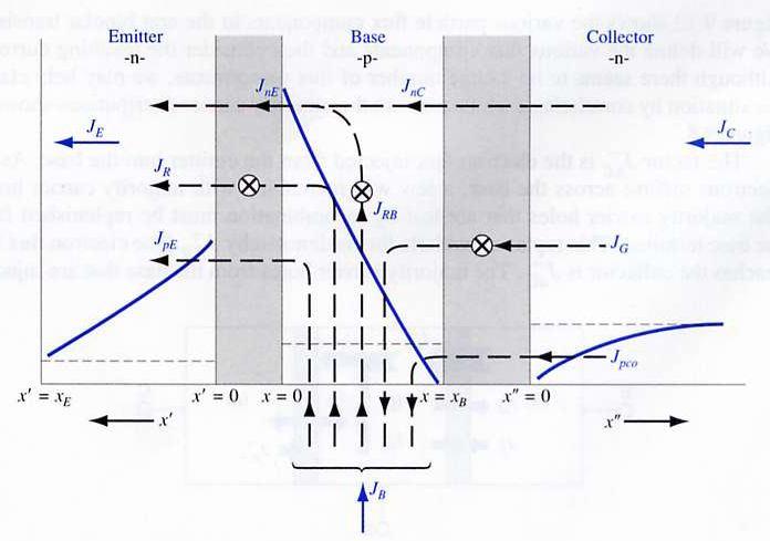
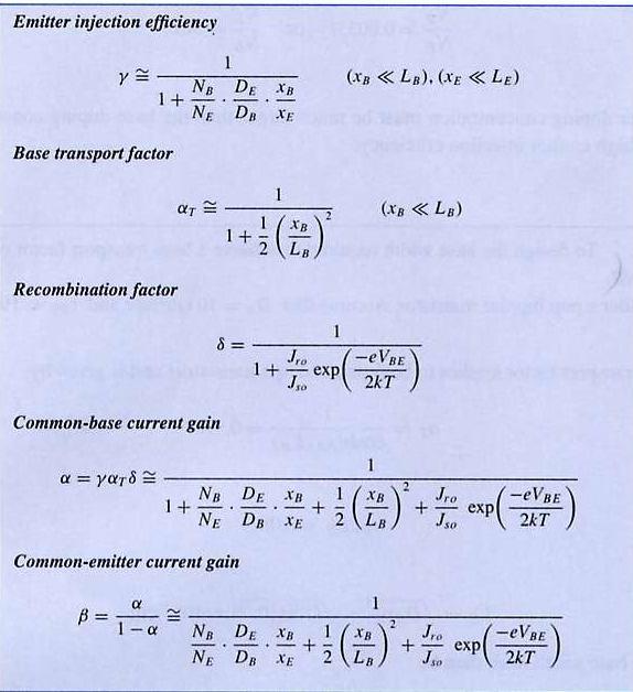
30 Low frequency common base current gain The basic operation of the BJT involves the control of the collector current by the B-E voltage The collector current is a function of the number of majority carriers reaching the collector after being injected from the emitter across the B-E junction The common-base current gain is defined as the ratio of Collector current to emitter current We need to consider the current terms involved in this value Begin by considering the various flux components in the npn transistor

31 Question Name, and explain the origin of, each of the terms in the diagram above
32
33
34 The currents J RB, J pe and J R are B-E junction currents and do not contribute to the collector current. The currents J pc0 and J G are B-C junction currents only. These current components do not contribute to the transistor action or the current gain. The dc common base current gain is defined as If we assume that the active cross-sectional area is the same for the collector and emitter, then
35 We are primarily interested in finding how the collector current will change with a change in the emitter current. The small signal, or sinusoidal, common base current gain is defined as This can be re-written as Equation 1
36 Where We would like to have the change in the collector current to be the same as the change in the emitter current, ie = 1. To get close to this each term equation 1 above must be as close to 1 as possible.
37 The emitter injection efficiency factor takes into account the minority hole diffusion current in the emitter. This current is part of the emitter current, but does not contribute to the transistor action in that J pe is not part of the collector current. The base transport factor takes into account any recombination of excess minority carrier electrons in the base. Ideally we want no recombination. The recombination factor takes into account the recombination in the forward biased B-E junction. This current, J R, contributes to the emitter current but does not contribute to the collector current. We now need to determine each of the gain factors in terms of the electrical and geometrical parameters of the transistor - this will enable us to design the effective BJTs
38 Emitter injection efficiency factor We can write the current densities as
39 Taking derivatives then gives us If we assume that the B-E junction is sufficiently far in In the forward bias regime so that V BE >>kt/e, then
40 and also The emitter injection efficiency then becomes
41 If we assume that all of the parameters in this equation are fixed, except for p E0 and n B0, then in order that is close to unity, we must have p E0 << n B0. We can write, where N E and N B are the impurity doping concentrations in the emitter and base. This then implies that N E >> N B. If both x B << L B and x E << L E then the emitter injection efficiency can be written as
42 Base Transport factor From the definitions of the current directions we used above we can write, If we then consider the expression we had for n B (x) before, we find that
43 Again assume that the B-E junction is biased sufficiently far in the forward region so that V BE >> kt/e, then exp(ev BE /kt) >> 1, substitution then gives, For T to be close to unity, the neutral base width x B must be much smaller than the minority carrier diffusion length in the base L B.
44 If x B << L B, then cosh(x B /L B ) will be just slightly greater than unity, and if exp(ev BE /kt) >> 1, the base transport factor will approximate to, For x B << L B, we can expand the cosh function in a Taylor series, so that So, the base transport factor will be close to one if x B << L B
45 Recombination factor If we assume J pe << J ne, then we can write The recombination current density due to the recombination in a forward biased p-n junction is as derived earlier in the course, and can be written as, where x BE is the B-E space charge width

46 The current J ne can be approximated to where The recombination factor can then be written as

47 The recombination factor is a function of the B-E voltage. As V BE increases, the recombination current becomes less dominant and the recombination factor approaches unity The recombination factor must also include surface effects; the figure below shows the B-E junction of an npn transistor near the semiconductor surface Assume the B-E junction is forward biased - the excess minority carrier concentration in the base along the cross section A-A will be,
48 This curve represents the normal forward-biased junction minority carrier concentration. However, the cross section at C-C from the surface will be,

49 The excess concentration at the surface is smaller than the excess concentration in the bulk - this causes an electron Diffusion current to occur from the bulk to the surface, where the electrons recombine with the majority carrier holes. This additional recombination current must be included in the recombination factor - difficult to calculate due to the 2-D nature
50 Although the have been considering an npn transistor, the same analysis for all of these transport factors applies to pnp devices We have also been considering the common base current gain, but we can also consider the common emitter current gain which is defined as The relation between the common base and common emitter current gains comes from,
51 Since this relationship holds for both dc and small-signal conditions, we can drop the subscript and write, and then the common base current gain in terms of the common emitter current gain is found to be,
52
53 If we assume a typical values of to be 100, then will equal If we also assume, = T = then each factor would have to be equal to to get a value of 100 This simple calculation indicates just how close to unity each factor must be in order to achieve a reasonable current gain Questions Give a qualitative explanation of current gain in a BJT Describe the key device design factors involved in achieving high current gain in a BJT
54 Qualitative arguments We can see that a current of electrons flows out of the emitter and if only a few of these recombine in the base then we will have a collector current of almost the same magnitude (forward active mode) There will also be a small current of holes flowing into the base from the external contact, to account for charge neutrality as some recombination does occur The key to using the device as a amplifier is to use this base current to control the collector current Consider the effect of applying a small current of holes to the base These excess holes will introduce a small positive charge into the base
55 Electrons must therefore flow from the emitter to the base to counter this current (can not be from the collector as this junction is reverse biased) Since most of the electrons from the emitter flow through the base without recombination, the number electrons flowing from the emitter must greatly exceed the number of holes flowing into the base For example, if we assume only 1% of electrons recombine with a hole, then 99% continue into the collector; if we vary the base current, the current of electrons flowing from the emitter to the collector varies accordingly, in direct proportion to the current flowing in at the base The difference is that the collector current is much larger than the base current, here 99x larger
56 Hence, if we use this device in a situation where the base current serves as the input and the collector current as the output, then the transistor acts as an amplifier But - how is it that we can convert a weak signal into a Strong one? Normally, there is no free lunch the large current is already present - it is the current applied to the emitter of the transistor the function of the transistor is simply to imprint the pattern of the weak signal onto this large current to produce a much stronger signal This leads us to the limitation on this type of device If the base current is too large then the voltage across the emitter will not be sufficient to supply the required number of electrons SATURATION
57 Example 1 Design the ratio of emitter doping to base doping in a BJT to achieve an emitter injection efficiency factor equal to = (npn device) For simplicity assume D E = D B, L E = L B and x E = x B From the equations above we have,
58 So, then, Hence, the emitter doping concentration must be much larger than the base doping concentration to achieve a high emitter injection efficiency
59 Example 2 Design the base width required to achieve a base transport factor equal to T = (pnp device) Assume that D B = 10 cm 2 /sec and B0 equals 10-7 sec The base transport factor is given by,
60 If the base width is less than approx. 0.8µm, then the required base transport factor will be achieved. In most cases, the base transport factor will not be the limiting factor in the BJT current gain Example 3 Calculate the forward-biased B-E voltage required to achieve a recombination factor equal to Consider an npn transistor at 300K. Assume that J S0 = A/cm 2
61 We then have Re-arranging this gives
62 This example demonstrates that the recombination factor may be an important limiting factor in the BJT gain. Here, if V BE is smaller than 0.654V, then the recombination factor will fall below the desired value. Example 4 Calculate the common-emitter current gain of a silicon npn BJT, taking T = 300K. Assume the following parameters,
63 We can calculate,
64 The emitter injection efficiency factor will be, We now need to calculate the base transport factor, again using the equation we derived earlier, and then the recombination factor
65 Where J S0 can be calculated from,
66 We can now calculate that = The common-base current gain is then, which gives a common-emitter current gain of In this example we can see that the emitter injection efficiency is the limiting factor in the current gain level we can achieve
67 Real BJTs - the influence of non-ideality We have been considering a BJT which has Uniform doped regions Low injection Constant emitter and base widths An ideal constant energy band-gap Uniform current densities The absence of junction breakdown If any of these conditions are not met, then the BJT properties will deviate from those we have been calculating It is therefore important to consider the likely effect of deviation from the ideal in each case
68 Base width modulation - the Early effect We have been assuming that the neutral base width x B is constant. However, in practice it will be a function of the B-C junction voltage, since the width of the space charge region extending into the base varies with V BC Increasing V BC (reverse bias), increases the space charge region width This reduces x B This will cause an increase in the concentration gradient in the base region, caused by the injection of minority carriers from the emitter This will increase the diffusion current through the base This results in an increase in the collector current This is known as the Early effect; Early being the First person to identify the problem
69 The change in the base width and the change in the minority carrier concentration gradient, as the B-C space charge width changes is illustrated below,
70 The Early effect is illustrated below, where the collector current is plotted against the C-E voltage - the extent to which a structure is influenced by the Early effect is represented by the Early voltage, also shown
71 Ideally the collector current is independent of the B-C voltage, so the slope in the above graphs would be zero The Early effect gives a non-zero slope and leads to a finite output conductance If the collector current characteristics are extrapolated to zero collector current, the curves intersect the voltage axis at a point defined as the Early voltage, which is considered to have a positive value This is an important parameter in transistor design Typical values are in the volt range The actual design used will determine the value, and hence determine the user specifications within a given circuit
72 We can write that, Where V A and V CE are defined as positive quantities and g 0 is defined as the output conductance. We can now re-write the above equation, showing explicitly that the collector current is now a function of the C-E voltage or the C-B voltage
73 Questions How would you use the doping levels in an npn structure to influence the Early voltage? In what way would you change them to reduce the Early voltage? What would be the influence of increasing the base width? What other, perhaps competing, effect would this have? Example 5 Calculate the change in the neutral base width with a change in the C-B voltage Consider a uniformly doped npn BJT at 300K
74 Assume a base doping level of 5 x cm -3 and a collector doping level of 2 x cm -3, taking a metallurgical base width of 0.70µm Calculate the neutral base width as the C-B voltage changes from 2 to 10 volts The space charge width extending into the base region can be written as,
75 or The built-in potential is,
76 For V CB = 2 volts, we find x db = 0.052µm, and for V CB = 10 volts, we find x db = 0.103µm If we neglect the B-E space charge region, which is small as The junction is in forward bias, we can calculate the neutral Base width For V CB = 2 volts For V CB = 10 volts This example shows that the neutral base width can change by 8% as V CB goes from 2 to 10 volts
77 Example 6 Calculate the change in the collector current with a change in the neutral base width, and estimate the Early voltage Consider a uniformly doped Si npn BJT, with parameters as determined in example 5. Assume D B = 25cm 2 /sec, V BE = 0.60V, and that x B << L B The excess minority carrier electron concentration in the base is given by,
78 If x B << L B, then (x B -x) << L B so we can approximate, The expression for n B (x) can then be approximated as, and the collector current is now,
79 The value of n B0 is calculated as, If we let x B = 0.648µm when V CB = 2V, then, with V CB = 10V, this becomes 3.47 A/cm 2 We can write
80 Which gives us, and the Early voltage is then, This example indicates how much the collector current can change as the neutral base width changes with a change in the B-C space charge width, and also illustrates the value of a typical Early voltage
81 High injection So far we have assumed low injection conditions the minority carrier concentration in the base remains low compared to the majority carrier concentration As V BE increases, the injected minority carrier concentration may approach or even exceed the majority carrier Concentration This will cause two things to happen Reduction in emitter efficiency The collector current will increase at a slower rate as V BE increases, in effect an increased series resistance is created
82 If we assume quasi-charge neutrality, then the majority carrier hole concentration in the p-base will increase due to the excess holes as shown below,
83 First effect - reduction in emitter efficiency Since the majority carrier hole concentration at x = 0 increases with high injection, more holes are injected back into the emitter due to the forward biased B-e voltage An increase in hole injection causes an increase in the J PE current and an increase in J PE reduces the emitter injection efficiency Hence, the common emitter current gain decreases under conditions of high injection This is illustrated below, where the common emitter gain For a typical BJT is plotted against collector current The low gain at low currents is due to the small recombination factor and the drop-off at the high current is due to the high injection effect
84
85 Second effect - slower increase in collector current with V BE At low injection the majority carrier hole concentration at x =0 for the npn BJT is, and the minority carrier electron concentration is, The p-n product is,
86 At high injection this last equation still applies. However, p P (0) will also increase, and for very high injection it will increase at nearly the same rate as n P (0) This will asymptotically approach the function The excess minority carrier concentration in the base, and hence the collector current, will increase at a slower rate with B-E voltage in high injection than low injection The high injection effect is very similar to the effect of a series resistance in a p-n junction diode
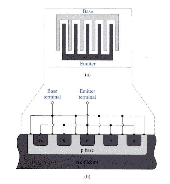
87 Collector current vs base-emitter voltage showing high injection effects
88 Emitter bandgap narrowing As silicon becomes heavily doped the discrete donor energy Level in an n-type emitter splits into a band of energies The distance between donor atoms decreases as the concentration increases, and the splitting is caused by the interaction of the donor atoms with each other As the doping continues to increase, the donor band widens, becomes skewed, and moves upward towards the conduction band edge, eventually merging with it At this point the effective band gap has decreased
89
90 A reduction in the bandgap energy increases the intrinsic carrier concentration, In a heavily doped emitter, the intrinsic carrier concentration can be written as, where E g0 is the bandgap energy at a low doping concentration and E g is the bandgap narrowing factor
91 The emitter injection efficiency factor is (as before), The term P E0 is the thermal-equilibrium minority carrier concentration in the emitter and can be written as, As the emitter doping increases, E g increases, thus p E0 does not continue to decrease with emitter doping - ie emitter injection efficiency begins to fall off rather than increasing with emitter doping
92 Example 7 Determine the increase in P E0 in emitter doping due to bandgap narrowing Consider a silicon emitter at T=300K, assume the emitter doping increases from to cm -3 Neglecting bandgap narrowing we have, for each respectively,
93 Taking into account the bandgap narrowing we obtain, Hence, if the emitter doping increases in this way, the thermal equilibrium minority carrier concentration actually increases by a factor of 1.5, rather than decreasing by the expected factor of 10. This effect is due to bandgap narrowing This leads the emitter injection efficiency to decrease, and hence the transistor gain decreases compared to the value we expect

94 Current crowding The base region is generally <1µm thick, so there can be a significant base resistance The non-zero base resistance results in a lateral potential difference under the emitter region
95 For an npn transistor, the potential decreases from the edge Of the emitter toward the centre The emitter is highly doped so to a first approx. can be considered an equipotential region The number of electrons from the emitter injected into the Base is exponentially dependent on V BE With the lateral drop in the base between the edge and centre of the emitter, more electrons will be injected near the emitter edges than the emitter centre This causes current crowding The larger current density near the emitter edge may cause localised heating and localised high injection effects

96 The non-uniform emitter current also results in a non-uniform Lateral base current under the emitter A 2-D analysis would be required to calculate the actual PD vs distance bacuse of this Power transistors require large emitter areas to maintain reasonable current desnsities, to avoid current-crowding these transistors are usually designed with narrow emitter widths and fabricated with an interdigitated design - in effect many narrow emitters are connected in parallel to achieve the required emitter area
97
98 Non-uniform base doping We have assumed uniformly doped regions in our BJTs so far Technology limitations mean this is rarely the case
99 Questions Why are these profiles typical in terms of the doping technology used? What could we do to make them more linear? A graded impurity concentration leads to an induced electric field. For a p-type base region we can write,
100 Then, Electrons are injected from the n-type emitter into the base and the minority carrier base electrons begin diffusing towards The collector region The induced electric field in the base, due to nonuniform doping, produces a force on the electrons in the direction toward the collector This drift current is thus an aid to the existing diffusion current, although the total current across the base will remain constant
101 The induced electric field due to non-uniform doping will alter the minority carrier distribution throughout the base so that the sum of the drift and diffusion currents become a constant Uniform base doping theory remains useful in estimating base characteristics The principal effect is a reduction in the likelihood of device breakdown through punch-through Breakdown Voltage Two mechanisms must be considered Punch-through Avalanche breakdown
102 Punch-through As the reverse-bias B-C voltage increases, the depletion region encroaches further into the base and can eventually occupy all of it This will cause a large surge in collector current and loss of transistor action Neglecting the contribution to base narrowing from the forward biased E-B junction, punch-through will occur when x db = W B where,
103 where V pt is the reverse-biased B-C voltage at punch-through negelecting V bi compared to V pt, we can solve V pt as, Example 8 Design the collector doping and collector width of a BJT to meet a punch-through voltage specification Consider a uniformly doped Si BJT with a metallurgical base width of 0.5µm, and a base doping level of N B = cm -3. The punch-through voltage is to be V pt = 25V.
104 The maximum collector doping concentration can be determined as, We can then determine,
105 Avalanche breakdown - tends to occur at much higher potentials than punch-through for most BJT designs, so is less important
106 Frequency limitations We need to consider two effects Time-delay factors Transistor cut-off frequency The BJT is a transit time device. When a voltage across the B-E junction increases, additional carriers are created in the base, they must then diffuse and be collected in the collector Region As the frequency increases the transit time will become appreciable compared to the period of the input signal Output will no longer be in phase with the input and the current gain will decrease

107 The total emitter-to-collector constant or time delay can be written as, The common-base current gain as a function of frequency can be written as,
108 Where 0 is the low frequency common base current gain and f is defined as the alpha cutoff frequency, which is related to the emitter to collector delay EC as When the frequency is equal to the alpha cutoff frequency, the magnitude of the common-base current gain is of it low frequency value
109 We can relate the alpha cutoff frequency to the common emitter current gain by considering, Where we have assumed 0 ~ 1. When the signal frequency is equal to f, the magnitude of the common emitter current gain is equal to 1, defined as the cutoff frequency, f T
110 We can also write the common emitter current gain as, where f is called the beta cutoff frequency Combining these equations gives,
111 and hence the beta cutoff frequency is related to the cutoff frequency by,
112 This is a Bode plot of the common emitter current gain as a function of frequency Note the log scale, so f and f T usually have very different values
113 Example 12 Calculate the emitter-to-collector transit time and the cutoff frequency of a silicon BJT at 300K given, Initially calculate the various time-delay factors. Neglecting parasitic capacitance, the emitter-base junction charging time is,
114 where The base transit time is The collector depletion region transit time is,
115 The collector capacitance charging time is The total emitter-to-collector time delay is then
116 so that the cutoff frequency is calculated as If we assume a low-frequency common emitter current gain of = 100, then the beta cutoff frequency is We can conclude that high-frequency BJTs need small device geometries in order to reduce capacitances, and narrow base widths in order to reduce the base transit time
117 Revision problems For a uniformly doped n + pn BJT in thermal equilibrium (a) Sketch the energy band-diagram (b) Sketch the electric field through the device (c) Repeat parts (a) and (b) for the transistor in the forward active region A uniformly doped silicon npn BJT is to be biased in the Forward-active mode with the B-C junction reverse biased At 3 volts. The metallurgical base width is 1.10µm. The transistor doping levels are N E = 10 17, N B = and N C = cm -3. (a) Calculate the B-E voltage at which the minority carrier electron concentration at x=0 is 10% of the majority hole concentration (b) At this bias, determine the minority carrier hole concentration at x =0 (c) Determine the neutral base width for this bias
Review Energy Bands Carrier Density & Mobility Carrier Transport Generation and Recombination
 Review Energy Bands Carrier Density & Mobility Carrier Transport Generation and Recombination Current Transport: Diffusion, Thermionic Emission & Tunneling For Diffusion current, the depletion layer is
Department of Electrical Engineering IIT Madras
 Department of Electrical Engineering IIT Madras Sample Questions on Semiconductor Devices EE3 applicants who are interested to pursue their research in microelectronics devices area (fabrication and/or
Bipolar Junction Transistors (BJTs) Overview
 Overview") 1 Bipolar Junction Transistors (BJTs) Asst. Prof. MONTREE SIRIPRUCHYANUN, D. Eng. Dept. of Teacher Training in Electrical Engineering, Faculty of Technical Education King Mongkut s Institute of Technology
1 Bipolar Junction Transistors (BJTs) Asst. Prof. MONTREE SIRIPRUCHYANUN, D. Eng. Dept. of Teacher Training in Electrical Engineering, Faculty of Technical Education King Mongkut s Institute of Technology
Basic Electronics Prof. Dr. Chitralekha Mahanta Department of Electronics and Communication Engineering Indian Institute of Technology, Guwahati
 Basic Electronics Prof. Dr. Chitralekha Mahanta Department of Electronics and Communication Engineering Indian Institute of Technology, Guwahati Module: 2 Bipolar Junction Transistors Lecture-1 Transistor
(Refer Slide Time: 01:33)
") Solid State Devices Dr. S. Karmalkar Department of Electronics and Communication Engineering Indian Institute of Technology, Madras Lecture - 31 Bipolar Junction Transistor (Contd ) So, we have been discussing
Solid State Devices Dr. S. Karmalkar Department of Electronics and Communication Engineering Indian Institute of Technology, Madras Lecture - 31 Bipolar Junction Transistor (Contd ) So, we have been discussing
ELEC 3908, Physical Electronics, Lecture 16. Bipolar Transistor Operation
 ELEC 3908, Physical Electronics, Lecture 16 Bipolar Transistor Operation Lecture Outline Last lecture discussed the structure and fabrication of a double diffused bipolar transistor Now examine current
CHAPTER 8 The PN Junction Diode
 CHAPTER 8 The PN Junction Diode Consider the process by which the potential barrier of a PN junction is lowered when a forward bias voltage is applied, so holes and electrons can flow across the junction
NAME: Last First Signature
 UNIVERSITY OF CALIFORNIA, BERKELEY College of Engineering Department of Electrical Engineering and Computer Sciences EE 130: IC Devices Spring 2003 FINAL EXAMINATION NAME: Last First Signature STUDENT
Lecture - 18 Transistors
 Electronic Materials, Devices and Fabrication Dr. S. Prarasuraman Department of Metallurgical and Materials Engineering Indian Institute of Technology, Madras Lecture - 18 Transistors Last couple of classes
CHAPTER 8 The PN Junction Diode
 CHAPTER 8 The PN Junction Diode Consider the process by which the potential barrier of a PN junction is lowered when a forward bias voltage is applied, so holes and electrons can flow across the junction
PN Junction in equilibrium
 PN Junction in equilibrium PN junctions are important for the following reasons: (i) PN junction is an important semiconductor device in itself and used in a wide variety of applications such as rectifiers,
CHAPTER 8 The pn Junction Diode
 CHAPTER 8 The pn Junction Diode Consider the process by which the potential barrier of a pn junction is lowered when a forward bias voltage is applied, so holes and electrons can flow across the junction
ECE 440 Lecture 29 : Introduction to the BJT-I Class Outline:
 ECE 440 Lecture 29 : Introduction to the BJT-I Class Outline: Narrow-Base Diode BJT Fundamentals BJT Amplification Things you should know when you leave Key Questions How does the narrow-base diode multiply
UNIT 3: FIELD EFFECT TRANSISTORS
 FIELD EFFECT TRANSISTOR: UNIT 3: FIELD EFFECT TRANSISTORS The field effect transistor is a semiconductor device, which depends for its operation on the control of current by an electric field. There are
UNIT 3 Transistors JFET
 UNIT 3 Transistors JFET Mosfet Definition of BJT A bipolar junction transistor is a three terminal semiconductor device consisting of two p-n junctions which is able to amplify or magnify a signal. It
CONTENTS. 2.2 Schrodinger's Wave Equation 31. PART I Semiconductor Material Properties. 2.3 Applications of Schrodinger's Wave Equation 34
 CONTENTS Preface x Prologue Semiconductors and the Integrated Circuit xvii PART I Semiconductor Material Properties CHAPTER 1 The Crystal Structure of Solids 1 1.0 Preview 1 1.1 Semiconductor Materials
Digital Integrated Circuits A Design Perspective. The Devices. Digital Integrated Circuits 2nd Devices
 Digital Integrated Circuits A Design Perspective The Devices The Diode The diodes are rarely explicitly used in modern integrated circuits However, a MOS transistor contains at least two reverse biased
Power Bipolar Junction Transistors (BJTs)
") ECE442 Power Semiconductor Devices and Integrated Circuits Power Bipolar Junction Transistors (BJTs) Zheng Yang (ERF 3017, email: yangzhen@uic.edu) Power Bipolar Junction Transistor (BJT) Background The
ECE442 Power Semiconductor Devices and Integrated Circuits Power Bipolar Junction Transistors (BJTs) Zheng Yang (ERF 3017, email: yangzhen@uic.edu) Power Bipolar Junction Transistor (BJT) Background The
FIELD EFFECT TRANSISTOR (FET) 1. JUNCTION FIELD EFFECT TRANSISTOR (JFET)
 1. JUNCTION FIELD EFFECT TRANSISTOR (JFET)") FIELD EFFECT TRANSISTOR (FET) The field-effect transistor (FET) is a three-terminal device used for a variety of applications that match, to a large extent, those of the BJT transistor. Although there
FIELD EFFECT TRANSISTOR (FET) The field-effect transistor (FET) is a three-terminal device used for a variety of applications that match, to a large extent, those of the BJT transistor. Although there
semiconductor p-n junction Potential difference across the depletion region is called the built-in potential barrier, or built-in voltage:
 Chapter four The Equilibrium pn Junction The Electric field will create a force that will stop the diffusion of carriers reaches thermal equilibrium condition Potential difference across the depletion
I E I C since I B is very small
 Figure 2: Symbols and nomenclature of a (a) npn and (b) pnp transistor. The BJT consists of three regions, emitter, base, and collector. The emitter and collector are usually of one type of doping, while
UNIT-1 Bipolar Junction Transistors. Text Book:, Microelectronic Circuits 6 ed., by Sedra and Smith, Oxford Press
 UNIT-1 Bipolar Junction Transistors Text Book:, Microelectronic Circuits 6 ed., by Sedra and Smith, Oxford Press Figure 6.1 A simplified structure of the npn transistor. Microelectronic Circuits, Sixth
EC T34 ELECTRONIC DEVICES AND CIRCUITS
 RAJIV GANDHI COLLEGE OF ENGINEERING AND TECHNOLOGY PONDY-CUDDALORE MAIN ROAD, KIRUMAMPAKKAM-PUDUCHERRY DEPARTMENT OF ECE EC T34 ELECTRONIC DEVICES AND CIRCUITS II YEAR Mr.L.ARUNJEEVA., AP/ECE 1 PN JUNCTION
EJERCICIOS DE COMPONENTES ELECTRÓNICOS. 1 er cuatrimestre
 EJECICIOS DE COMPONENTES ELECTÓNICOS. 1 er cuatrimestre 2 o Ingeniería Electrónica Industrial Juan Antonio Jiménez Tejada Índice 1. Basic concepts of Electronics 1 2. Passive components 1 3. Semiconductors.
Solid State Devices- Part- II. Module- IV
 Solid State Devices- Part- II Module- IV MOS Capacitor Two terminal MOS device MOS = Metal- Oxide- Semiconductor MOS capacitor - the heart of the MOSFET The MOS capacitor is used to induce charge at the
Bipolar Junction Transistor (BJT) Basics- GATE Problems
 Basics- GATE Problems") Bipolar Junction Transistor (BJT) Basics- GATE Problems One Mark Questions 1. The break down voltage of a transistor with its base open is BV CEO and that with emitter open is BV CBO, then (a) BV CEO =
Bipolar Junction Transistor (BJT) Basics- GATE Problems One Mark Questions 1. The break down voltage of a transistor with its base open is BV CEO and that with emitter open is BV CBO, then (a) BV CEO =
Power Semiconductor Devices
 TRADEMARK OF INNOVATION Power Semiconductor Devices Introduction This technical article is dedicated to the review of the following power electronics devices which act as solid-state switches in the circuits.
Microelectronic Circuits, Kyung Hee Univ. Spring, Bipolar Junction Transistors
 Bipolar Junction Transistors 1 Introduction physical structure of the bipolar transistor and how it works How the voltage between two terminals of the transistor controls the current that flows through
Lecture Course. SS Module PY4P03. Dr. P. Stamenov
 Semiconductor Devices - 2013 Lecture Course Part of SS Module PY4P03 Dr. P. Stamenov School of Physics and CRANN, Trinity College, Dublin 2, Ireland Hilary Term, TCD 01 st of Feb 13 Diode Current Components
Digital Electronics. By: FARHAD FARADJI, Ph.D. Assistant Professor, Electrical and Computer Engineering, K. N. Toosi University of Technology
 K. N. Toosi University of Technology Chapter 7. Field-Effect Transistors By: FARHAD FARADJI, Ph.D. Assistant Professor, Electrical and Computer Engineering, K. N. Toosi University of Technology http://wp.kntu.ac.ir/faradji/digitalelectronics.htm
SRM INSTITUTE OF SCIENCE AND TECHNOLOGY (DEEMED UNIVERSITY)
") SRM INSTITUTE OF SCIENCE AND TECHNOLOGY (DEEMED UNIVERSITY) QUESTION BANK I YEAR B.Tech (II Semester) ELECTRONIC DEVICES (COMMON FOR EC102, EE104, IC108, BM106) UNIT-I PART-A 1. What are intrinsic and
SRM INSTITUTE OF SCIENCE AND TECHNOLOGY (DEEMED UNIVERSITY) QUESTION BANK I YEAR B.Tech (II Semester) ELECTRONIC DEVICES (COMMON FOR EC102, EE104, IC108, BM106) UNIT-I PART-A 1. What are intrinsic and
COE/EE152: Basic Electronics. Lecture 5. Andrew Selasi Agbemenu. Outline
 COE/EE152: Basic Electronics Lecture 5 Andrew Selasi Agbemenu 1 Outline Physical Structure of BJT Two Diode Analogy Modes of Operation Forward Active Mode of BJTs BJT Configurations Early Effect Large
BJT. Bipolar Junction Transistor BJT BJT 11/6/2018. Dr. Satish Chandra, Assistant Professor, P P N College, Kanpur 1
 BJT Bipolar Junction Transistor Satish Chandra Assistant Professor Department of Physics P P N College, Kanpur www.satish0402.weebly.com The Bipolar Junction Transistor is a semiconductor device which
Lecture 2 p-n junction Diode characteristics. By Asst. Prof Dr. Jassim K. Hmood
 Electronic I Lecture 2 p-n junction Diode characteristics By Asst. Prof Dr. Jassim K. Hmood THE p-n JUNCTION DIODE The pn junction diode is formed by fabrication of a p-type semiconductor region in intimate
Semiconductor Devices
 Semiconductor Devices Modelling and Technology Source Electrons Gate Holes Drain Insulator Nandita DasGupta Amitava DasGupta SEMICONDUCTOR DEVICES Modelling and Technology NANDITA DASGUPTA Professor Department
Lecture 16. The Bipolar Junction Transistor (I) Forward Active Regime. Outline. The Bipolar Junction Transistor (BJT): structure and basic operation
 Forward Active Regime. Outline. The Bipolar Junction Transistor (BJT): structure and basic operation") Lecture 16 The Bipolar Junction Transistor (I) Forward Active Regime Outline The Bipolar Junction Transistor (BJT): structure and basic operation I-V characteristics in forward active regime Reading Assignment:
Lecture 16 The Bipolar Junction Transistor (I) Forward Active Regime Outline The Bipolar Junction Transistor (BJT): structure and basic operation I-V characteristics in forward active regime Reading Assignment:
Chapter 8. Field Effect Transistor
 Chapter 8. Field Effect Transistor Field Effect Transistor: The field effect transistor is a semiconductor device, which depends for its operation on the control of current by an electric field. There
THE JFET. Script. Discuss the JFET and how it differs from the BJT. Describe the basic structure of n-channel and p -channel JFETs
 Course: B.Sc. Applied Physical Science (Computer Science) Year & Sem.: Ist Year, Sem - IInd Subject: Electronics Paper No.: V Paper Title: Analog Circuits Lecture No.: 12 Lecture Title: Analog Circuits
Lecture 24: Bipolar Junction Transistors (1) Bipolar Junction Structure, Operating Regions, Biasing
 Bipolar Junction Structure, Operating Regions, Biasing") Lecture 24: Bipolar Junction Transistors (1) Bipolar Junction Structure, Operating Regions, Biasing BJT Structure the BJT is formed by doping three semiconductor regions (emitter, base, and collector)
Lecture 24: Bipolar Junction Transistors (1) Bipolar Junction Structure, Operating Regions, Biasing BJT Structure the BJT is formed by doping three semiconductor regions (emitter, base, and collector)
ET215 Devices I Unit 4A
 ITT Technical Institute ET215 Devices I Unit 4A Chapter 3, Section 3.1-3.2 This unit is divided into two parts; Unit 4A and Unit 4B Chapter 3 Section 3.1 Structure of Bipolar Junction Transistors The basic
Lecture 3: Transistors
 Lecture 3: Transistors Now that we know about diodes, let s put two of them together, as follows: collector base emitter n p n moderately doped lightly doped, and very thin heavily doped At first glance,
Electronics I - Physics of Bipolar Transistors
 Chapter 5 Electronics I - Physics of Bipolar Transistors B E N+ P N- C B E C Fall 2017 claudio talarico 1 source: Sedra & Smith Thin Base Types of Bipolar Transistors n+ p n- Figure - A simplified structure
Reg. No. : Question Paper Code : B.E./B.Tech. DEGREE EXAMINATION, NOVEMBER/DECEMBER Second Semester
 WK 5 Reg. No. : Question Paper Code : 27184 B.E./B.Tech. DEGREE EXAMINATION, NOVEMBER/DECEMBER 2015. Time : Three hours Second Semester Electronics and Communication Engineering EC 6201 ELECTRONIC DEVICES
Lecture 12. Bipolar Junction Transistor (BJT) BJT 1-1
 BJT 1-1") Lecture 12 Bipolar Junction Transistor (BJT) BJT 1-1 Course Info Lecture hours: 4 Two Lectures weekly (Saturdays and Wednesdays) Location: K2 Time: 1:40 pm Tutorial hours: 2 One tutorial class every week
Lecture 12 Bipolar Junction Transistor (BJT) BJT 1-1 Course Info Lecture hours: 4 Two Lectures weekly (Saturdays and Wednesdays) Location: K2 Time: 1:40 pm Tutorial hours: 2 One tutorial class every week
Lesson 5. Electronics: Semiconductors Doping p-n Junction Diode Half Wave and Full Wave Rectification Introduction to Transistors-
 Lesson 5 Electronics: Semiconductors Doping p-n Junction Diode Half Wave and Full Wave Rectification Introduction to Transistors- Types and Connections Semiconductors Semiconductors If there are many free
Fundamentals of Power Semiconductor Devices
 В. Jayant Baliga Fundamentals of Power Semiconductor Devices 4y Spri ringer Contents Preface vii Chapter 1 Introduction 1 1.1 Ideal and Typical Power Switching Waveforms 3 1.2 Ideal and Typical Power Device
Analog & Digital Electronics Course No: PH-218
 Analog & Digital Electronics Course No: PH-218 Lec-5: Bipolar Junction Transistor (BJT) Course nstructors: Dr. A. P. VAJPEY Department of Physics, ndian nstitute of Technology Guwahati, ndia 1 Bipolar
Alexandria University Faculty of Engineering Electrical Engineering Department
 Chapter 10: Alexandria University Faculty of Engineering Electrical Engineering Department ECE 336: Semiconductor Devices Sheet 6 1. A Si pnp BJT with N AE = 5x10 17 / cm 3, N DB = 10 15 /cm 3 and N AC
Analog Electronics. Electronic Devices, 9th edition Thomas L. Floyd Pearson Education. Upper Saddle River, NJ, All rights reserved.
 Analog Electronics BJT Structure The BJT has three regions called the emitter, base, and collector. Between the regions are junctions as indicated. The base is a thin lightly doped region compared to the
Key Questions. ECE 340 Lecture 39 : Introduction to the BJT-II 4/28/14. Class Outline: Fabrication of BJTs BJT Operation
 Things you should know when you leave ECE 340 Lecture 39 : Introduction to the BJT-II Fabrication of BJTs Class Outline: Key Questions What elements make up the base current? What do the carrier distributions
Student Lecture by: Giangiacomo Groppi Joel Cassell Pierre Berthelot September 28 th 2004
 Student Lecture by: Giangiacomo Groppi Joel Cassell Pierre Berthelot September 28 th 2004 Lecture outline Historical introduction Semiconductor devices overview Bipolar Junction Transistor (BJT) Field
Bipolar Junction Transistor (BJT)
") Bipolar Junction Transistor (BJT) - three terminal device - output port controlled by current flow into input port Structure - three layer sandwich of n-type and p-type material - npn and pnp transistors
Bipolar Junction Transistor (BJT) - three terminal device - output port controlled by current flow into input port Structure - three layer sandwich of n-type and p-type material - npn and pnp transistors
Chapter 3 Bipolar Junction Transistors (BJT)
") Chapter 3 Bipolar Junction Transistors (BJT) Transistors In analog circuits, transistors are used in amplifiers and linear regulated power supplies. In digital circuits they function as electrical switches,
Chapter 3 Bipolar Junction Transistors (BJT) Transistors In analog circuits, transistors are used in amplifiers and linear regulated power supplies. In digital circuits they function as electrical switches,
Unless otherwise specified, assume room temperature (T = 300 K).
.") ECE 3040 Dr. Doolittle Homework 4 Unless otherwise specified, assume room temperature (T = 300 K). 1) Purpose: Understanding p-n junction band diagrams. Consider a p-n junction with N A = 5x10 14 cm -3
ECE 3040 Dr. Doolittle Homework 4 Unless otherwise specified, assume room temperature (T = 300 K). 1) Purpose: Understanding p-n junction band diagrams. Consider a p-n junction with N A = 5x10 14 cm -3
UNIT-VI FIELD EFFECT TRANSISTOR. 1. Explain about the Field Effect Transistor and also mention types of FET s.
 UNIT-I FIELD EFFECT TRANSISTOR 1. Explain about the Field Effect Transistor and also mention types of FET s. The Field Effect Transistor, or simply FET however, uses the voltage that is applied to their
(Refer Slide Time: 05:47)
") Solid State Devices Dr. S. Karmalkar Department of Electronics and Communication Engineering Indian Institute of Technology, Madras Lecture - 29 Bipolar Junction Transistor (Contd ) So we have been discussing
Solid State Devices Dr. S. Karmalkar Department of Electronics and Communication Engineering Indian Institute of Technology, Madras Lecture - 29 Bipolar Junction Transistor (Contd ) So we have been discussing
Introduction to semiconductor technology
 Introduction to semiconductor technology Outline 7 Field effect transistors MOS transistor current equation" MOS transistor channel mobility Substrate bias effect 7 Bipolar transistors Introduction Minority
Physics of Bipolar Transistor
 Physics of Bipolar Transistor Motivations - In many electronic applications, amplifier is the most fundamental building block. Ex Audio amplifier: amplifies electric signal to drive a speaker RF Power
7. Bipolar Junction Transistor
 41 7. Bipolar Junction Transistor 7.1. Objectives - To experimentally examine the principles of operation of bipolar junction transistor (BJT); - To measure basic characteristics of n-p-n silicon transistor
Semiconductor Devices Lecture 5, pn-junction Diode
 Semiconductor Devices Lecture 5, pn-junction Diode Content Contact potential Space charge region, Electric Field, depletion depth Current-Voltage characteristic Depletion layer capacitance Diffusion capacitance
6.012 Microelectronic Devices and Circuits
 Page 1 of 13 YOUR NAME Department of Electrical Engineering and Computer Science Massachusetts Institute of Technology 6.012 Microelectronic Devices and Circuits Final Eam Closed Book: Formula sheet provided;
EIE209 Basic Electronics. Transistor Devices. Contents BJT and FET Characteristics Operations. Prof. C.K. Tse: T ransistor devices
 EIE209 Basic Electronics Transistor Devices Contents BJT and FET Characteristics Operations 1 What is a transistor? Three-terminal device whose voltage-current relationship is controlled by a third voltage
Electronic devices-i. Difference between conductors, insulators and semiconductors
 Electronic devices-i Semiconductor Devices is one of the important and easy units in class XII CBSE Physics syllabus. It is easy to understand and learn. Generally the questions asked are simple. The unit
UNIT-III Bipolar Junction Transistor
 DC UNT-3.xplain the construction and working of JT. UNT- ipolar Junction Transistor A bipolar (junction) transistor (JT) is a three-terminal electronic device constructed of doped semiconductor material
MOS Field-Effect Transistors (MOSFETs)
") 6 MOS Field-Effect Transistors (MOSFETs) A three-terminal device that uses the voltages of the two terminals to control the current flowing in the third terminal. The basis for amplifier design. The basis
6 MOS Field-Effect Transistors (MOSFETs) A three-terminal device that uses the voltages of the two terminals to control the current flowing in the third terminal. The basis for amplifier design. The basis
THE METAL-SEMICONDUCTOR CONTACT
 THE METAL-SEMICONDUCTOR CONTACT PROBLEM 1 To calculate the theoretical barrier height, built-in potential barrier, and maximum electric field in a metal-semiconductor diode for zero applied bias. Consider
ECE 310 Microelectronics Circuits
 ECE 310 Microelectronics Circuits Bipolar Transistors Dr. Vishal Saxena (vishalsaxena@boisetstate.edu) Jan 20, 2014 Vishal Saxena 1 Bipolar Transistor n the chapter, we will study the physics of bipolar
Chapter Two "Bipolar Transistor Circuits"
 Chapter Two "Bipolar Transistor Circuits" 1.TRANSISTOR CONSTRUCTION:- The transistor is a three-layer semiconductor device consisting of either two n- and one p-type layers of material or two p- and one
Figure1: Basic BJT construction.
 Chapter 4: Bipolar Junction Transistors (BJTs) Bipolar Junction Transistor (BJT) Structure The BJT is constructed with three doped semiconductor regions separated by two pn junctions, as in Figure 1(a).
5.1 BJT Device Structure and Physical Operation
 11/28/2004 section 5_1 BJT Device Structure and Physical Operation blank 1/2 5.1 BJT Device Structure and Physical Operation Reading Assignment: pp. 377-392 Another kind of transistor is the Bipolar Junction
Simulation of MOSFETs, BJTs and JFETs. At and Near the Pinch-off Region. Xuan Yang
 Simulation of MOSFETs, BJTs and JFETs At and Near the Pinch-off Region by Xuan Yang A Thesis Presented in Partial Fulfillment of the Requirements for the Degree Master of Science Approved November 2011
EDC Lecture Notes UNIT-1
 P-N Junction Diode EDC Lecture Notes Diode: A pure silicon crystal or germanium crystal is known as an intrinsic semiconductor. There are not enough free electrons and holes in an intrinsic semi-conductor
The current density at a forward bias of 0.9 V is J( V) = 8:91 10 ;13 exp 0:06 = 9: :39=961:4 Acm ; 1: 10 ;8 exp 0:05 The current is dominated b
 = 8:91 10 ;13 exp 0:06 = 9: :39=961:4 Acm ; 1: 10 ;8 exp 0:05 The current is dominated b") Prof. Jasprit Singh Fall 000 EECS 30 Solutions to Homework 6 Problem 1 Two dierent processes are used to fabricate a Si p-n diode. The rst process results in a electron-hole recombination time via impurities
Prof. Jasprit Singh Fall 000 EECS 30 Solutions to Homework 6 Problem 1 Two dierent processes are used to fabricate a Si p-n diode. The rst process results in a electron-hole recombination time via impurities
Laboratory exercise: the Bipolar Transistor
 Laboratory exercise: the Bipolar Transistor Semiconductor Physics 2017 Lab meeting point k-space at Solid State Physics This exercise consists of two experimental parts and one simulation part. In the
EE70 - Intro. Electronics
 EE70 - Intro. Electronics Course website: ~/classes/ee70/fall05 Today s class agenda (November 28, 2005) review Serial/parallel resonant circuits Diode Field Effect Transistor (FET) f 0 = Qs = Qs = 1 2π
= ;7:05 10 ;13 The collector current is ead b n bo I C = sinh WB L B A = (1:6 10;19 C)(10 ; cm )(0 cm s ;1 )(: 10 3 cm ;3 ) (1:41 10 ;3 cm)(7:1 10 ; )
(10 ; cm )(0 cm s ;1 )(: 10 3 cm ;3 ) (1:41 10 ;3 cm)(7:1 10 ; )") Prof. Jasprit Singh Fall 001 EECS 30 Solutions to Homework 8 Problem 1: In a pnp silicon transistor at 300 K, the base doping is 5 10 16 cm ;3. The base width is 1.0 m and = 10.0 m. What is the total minority
Prof. Jasprit Singh Fall 001 EECS 30 Solutions to Homework 8 Problem 1: In a pnp silicon transistor at 300 K, the base doping is 5 10 16 cm ;3. The base width is 1.0 m and = 10.0 m. What is the total minority
R. W. Erickson. Department of Electrical, Computer, and Energy Engineering University of Colorado, Boulder
 R. W. Erickson Department of Electrical, Computer, and Energy Engineering University of Colorado, Boulder pn junction! Junction diode consisting of! p-doped silicon! n-doped silicon! A p-n junction where
UNIT IX ELECTRONIC DEVICES
 UNT X ELECTRONC DECES Weightage Marks : 07 Semiconductors Semiconductors diode-- characteristics in forward and reverse bias, diode as rectifier. - characteristics of LED, Photodiodes, solarcell and Zener
Lecture 4. Reading: Chapter EE105 Fall 2007 Lecture 4, Slide 1 Prof. Liu, UC Berkeley
 Lecture 4 OUTLNE Bipolar Junction Transistor (BJT) General considerations Structure Operation in active mode Large-signal model and - characteristics Reading: Chapter 4.1-4.4.2 EE105 Fall 2007 Lecture
The shape of the waveform will be the same, but its level is shifted either upward or downward. The values of the resistor R and capacitor C affect
 Diode as Clamper A clamping circuit is used to place either the positive or negative peak of a signal at a desired level. The dc component is simply added or subtracted to/from the input signal. The clamper
Shankersinh Vaghela Bapu Institute of Technology INDEX
 Shankersinh Vaghela Bapu Institute of Technology Diploma EE Semester III 3330905: ELECTRONIC COMPONENTS AND CIRCUITS INDEX Sr. No. Title Page Date Sign Grade 1 Obtain I-V characteristic of Diode. 2 To
Bipolar junction transistors.
 Bipolar junction transistors. Third Semester Course code : 15EECC202 Analog electronic circuits (AEC) Team: Dr. Nalini C Iyer, R.V. Hangal, Sujata N, Prashant A, Sneha Meti AEC Team, Faculty, School of
A study into the applicability of p þ n þ (universal contact) to power semiconductor diodes for faster reverse recovery
 to power semiconductor diodes for faster reverse recovery") Solid-State Electronics 47 (2003) 83 91 www.elsevier.com/locate/sse A study into the applicability of p þ n þ (universal contact) to power semiconductor diodes for faster reverse recovery R.S. Anand, B.
Solid-State Electronics 47 (2003) 83 91 www.elsevier.com/locate/sse A study into the applicability of p þ n þ (universal contact) to power semiconductor diodes for faster reverse recovery R.S. Anand, B.
ECE 3040 Dr. Alan Doolittle.
 ECE 3040 Dr. Alan Doolittle I have thoroughly enjoyed meeting each of you and hope that I have had a positive influence on your carriers. Please feel free to consult with me in your future work. If I can
FET. Field Effect Transistors ELEKTRONIKA KONTROL. Eka Maulana, ST, MT, M.Eng. Universitas Brawijaya. p + S n n-channel. Gate. Basic structure.
 FET Field Effect Transistors ELEKTRONIKA KONTROL Basic structure Gate G Source S n n-channel Cross section p + p + p + G Depletion region Drain D Eka Maulana, ST, MT, M.Eng. Universitas Brawijaya S Channel
 Electronic Devices 1. Current flowing in each of the following circuits A and respectively are: (Circuit 1) (Circuit 2) 1) 1A, 2A 2) 2A, 1A 3) 4A, 2A 4) 2A, 4A 2. Among the following one statement is not
NOVEL 4H-SIC BIPOLAR JUNCTION TRANSISTOR (BJT) WITH IMPROVED CURRENT GAIN
 WITH IMPROVED CURRENT GAIN") NOVEL 4H-SIC BIPOLAR JUNCTION TRANSISTOR (BJT) WITH IMPROVED CURRENT GAIN Thilini Daranagama 1, Vasantha Pathirana 2, Florin Udrea 3, Richard McMahon 4 1,2,3,4 The University of Cambridge, Cambridge, United
NOVEL 4H-SIC BIPOLAR JUNCTION TRANSISTOR (BJT) WITH IMPROVED CURRENT GAIN Thilini Daranagama 1, Vasantha Pathirana 2, Florin Udrea 3, Richard McMahon 4 1,2,3,4 The University of Cambridge, Cambridge, United
Transistor Characteristics
 Transistor Characteristics Topics covered in this presentation: Transistor Construction Transistor Operation Transistor Characteristics 1 of 15 The Transistor The transistor is a semiconductor device that
10/27/2009 Reading: Chapter 10 of Hambley Basic Device Physics Handout (optional)
") EE40 Lec 17 PN Junctions Prof. Nathan Cheung 10/27/2009 Reading: Chapter 10 of Hambley Basic Device Physics Handout (optional) Slide 1 PN Junctions Semiconductor Physics of pn junctions (for reference
EE40 Lec 17 PN Junctions Prof. Nathan Cheung 10/27/2009 Reading: Chapter 10 of Hambley Basic Device Physics Handout (optional) Slide 1 PN Junctions Semiconductor Physics of pn junctions (for reference
SUMMER 13 EXAMINATION Subject Code: Model Answer Page No: / N
 Important Instructions to examiners: 1) The answers should be examined by key words and not as word-to-word as given in the model answer scheme. 2) The model answer and the answer written by candidate
An Introduction to Bipolar Junction Transistors. Prepared by Dr Yonas M Gebremichael, 2005
 An Introduction to Bipolar Junction Transistors Transistors Transistors are three port devices used in most integrated circuits such as amplifiers. Non amplifying components we have seen so far, such as
FET(Field Effect Transistor)
") Field Effect Transistor: Construction and Characteristic of JFETs. Transfer Characteristic. CS,CD,CG amplifier and analysis of CS amplifier MOSFET (Depletion and Enhancement) Type, Transfer Characteristic,
Field Effect Transistor: Construction and Characteristic of JFETs. Transfer Characteristic. CS,CD,CG amplifier and analysis of CS amplifier MOSFET (Depletion and Enhancement) Type, Transfer Characteristic,
EE/COE 152: Basic Electronics. Lecture 3. A.S Agbemenu. https://sites.google.com/site/agbemenu/courses/ee-coe-152
 EE/COE 152: Basic Electronics Lecture 3 A.S Agbemenu https://sites.google.com/site/agbemenu/courses/ee-coe-152 Books: Microelcetronic Circuit Design (Jaeger/Blalock) Microelectronic Circuits (Sedra/Smith)
Field - Effect Transistor
 Page 1 of 6 Field - Effect Transistor Aim :- To draw and study the out put and transfer characteristics of the given FET and to determine its parameters. Apparatus :- FET, two variable power supplies,
Bipolar Junction Transistors
 Bipolar Junction Transistors Invented in 1948 at Bell Telephone laboratories Bipolar junction transistor (BJT) - one of the major three terminal devices Three terminal devices more useful than two terminal
KOM2751 Analog Electronics :: Dr. Muharrem Mercimek :: YTU - Control and Automation Dept. 1 2 (CONT D - II) DIODE APPLICATIONS
 DIODE APPLICATIONS") KOM2751 Analog Electronics :: Dr. Muharrem Mercimek :: YTU - Control and Automation Dept. 1 2 (CONT D - II) DIODE APPLICATIONS Most of the content is from the textbook: Electronic devices and circuit theory,
KOM2751 Analog Electronics :: Dr. Muharrem Mercimek :: YTU - Control and Automation Dept. 1 2 (CONT D - II) DIODE APPLICATIONS Most of the content is from the textbook: Electronic devices and circuit theory,
Lecture-45. MOS Field-Effect-Transistors Threshold voltage
 Lecture-45 MOS Field-Effect-Transistors 7.4. Threshold voltage In this section we summarize the calculation of the threshold voltage and discuss the dependence of the threshold voltage on the bias applied
(Refer Slide Time: 02:05)
") Electronics for Analog Signal Processing - I Prof. K. Radhakrishna Rao Department of Electrical Engineering Indian Institute of Technology Madras Lecture 27 Construction of a MOSFET (Refer Slide Time:
Electronics for Analog Signal Processing - I Prof. K. Radhakrishna Rao Department of Electrical Engineering Indian Institute of Technology Madras Lecture 27 Construction of a MOSFET (Refer Slide Time:
MTLE-6120: Advanced Electronic Properties of Materials. Semiconductor transistors for logic and memory. Reading: Kasap
 MTLE-6120: Advanced Electronic Properties of Materials 1 Semiconductor transistors for logic and memory Reading: Kasap 6.6-6.8 Vacuum tube diodes 2 Thermionic emission from cathode Electrons collected
Electronics The basics of semiconductor physics
 Electronics The basics of semiconductor physics Prof. Márta Rencz, Gábor Takács BME DED 17/09/2015 1 / 37 The basic properties of semiconductors Range of conductivity [Source: http://www.britannica.com]